Organic Semiconductor-based Plastic Solar Cells
73
Organic Materials for electronics & Photonics Organic Semiconductor-based Plastic Solar Cells
-
Upload
piyush-raj-saxena -
Category
Documents
-
view
21 -
download
1
description
Advanced form of solar panals
Transcript of Organic Semiconductor-based Plastic Solar Cells

Organic Materials for electronics & Photonics
Organic Semiconductor-based Plastic Solar Cells

Organic Materials for electronics & Photonics
Light energy (photons) Electrical energy
When sunlight is absorbed by some materials, the solar energy knocks electrons loose from their atoms, allowing the electrons to flow through the material to produce electricity. This process of converting light (photons) to electricity (voltage) is called the photovoltaic (PV) effect.
What’s PVs

Organic Materials for electronics & Photonics
At earth’s surface average solar energy is ~ 4 x 1024 J / yearGlobal energy consumption (2001) was ~ 4 x 10²⁰ J / year (increasing ~ 2% annually)
In US, average power requirement is 3.3 TW.With 10% efficient cells we would need 1.7% of land area devoted to PV (~ area occupied by interstate highways)
Source: DOE (U.S. Department of Energy) Source: N. Lewis (Caltech)
Solar energy

Organic Materials for electronics & Photonics
History
• 1839 : Finding of Photovoltaic effect with liquid (Edmond becquerel)• 1876 : Photovoltaic effect in a solid (Heinrich Hertz)• 1883 : Se solar cell (C. Fritts)• 1930 : Research of Cu2O/Cu solar cell • 1941 : Patent of Si solar cell (R. Ohl) • 1954 : Crystalline Si solar cell (Bell Lab.) ; 4 % efficiency • 1958 : Using as assistant power in the spaceship (Vanguard I ) ; 5 mW• 1973 : oil crisis• 1980 : solar cell using CdTe, CuInSe2 ,TiO2 etc.• 1997 : world product 100MWp • 2000 : research of an advanced materials and structures (dye sensitized solar cell, organic solar cell) cheap process , flexible substrate
Organic Materials for electronics & Photonics
p-type Semiconductor
Space charge region
n-type Semiconductor
Metal top electrode
Metal back contact
h (photon)
Photovoltaic (PV) effect
In a conventional semiconductor, light absorption generates an electric field that separates the photo-induced charges. Ec and Ev are the energies at the conduction and valence bands, respectively.

Organic Materials for electronics & Photonics
100S
mpmp
P
VI
ocsc
mpmp
VI
VIFF
100S
ocsc
P
FFVI
ISC : Short-circuit current
Current value when V = 0
VOC : Open-circuit voltage
Voltage value when I = 0
P : Power output of the cell
P = IV
F.F : Fill factor
Under AM 1.5G simulated solar illumination
)] ( )][( [
)] ( ][ 0124[
incidnet photons of no.
circuit external he through telectrons of no.
2
2
cmmWirradiancenmwavelength
cmAdensityntphotocurrenmeV
IPCE
< Power conversion efficiency (η) >
< Incident-photon-to-current conversion efficiency (IPCE) >
Cell efficiency
Organic Materials for electronics & Photonics
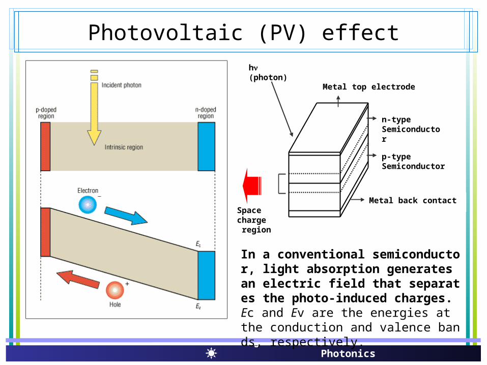
Air mass (AM)
θz

Organic Materials for electronics & Photonics
Sunlight spectrum
Global condition (G) : including the diffusion component (indirect component owing to scattering and reflection in the atmosphere and surrounding landscape)
Direct condition (D) : without the diffusion component

Organic Materials for electronics & Photonics
Classification
태양전지
실리콘 반도체 화합물 반도체 기타
결정계
비결정
계
다결
정
II VI• 족 CdS CdTe…
III V• 족 GaAs InP…
I•III•VI 족CuInSe2..
유기태양전
지 염료감응태양전
지
단결
정
Conventional inorganic p/n junction solar cell

Organic Materials for electronics & Photonics
Progress of cell efficiencies
Under AM 1.5G simulated solar illumination

Organic Materials for electronics & Photonics
PV systems installed in Korea

Organic Materials for electronics & Photonics
PV systems installed in Korea
Organic Materials for electronics & Photonics
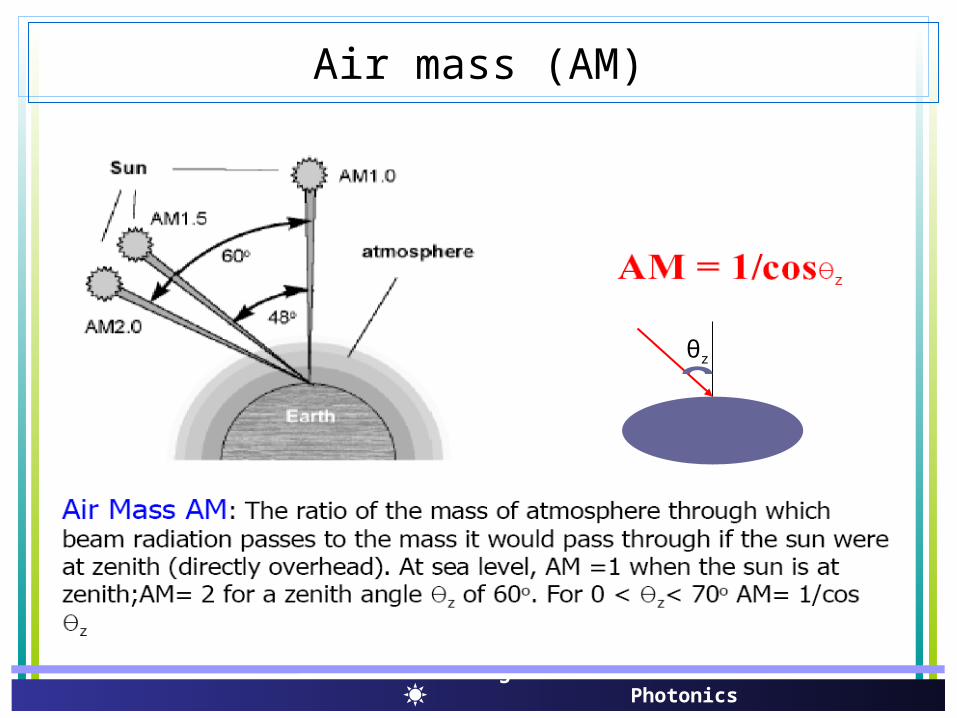
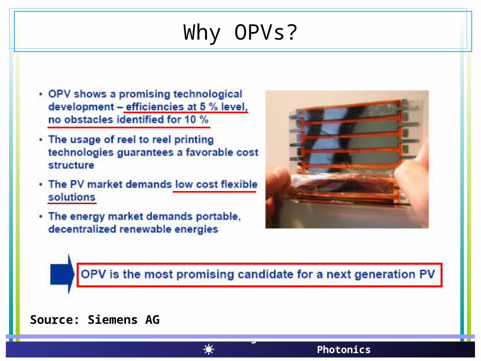
Advantages of Organic PVs (OPVs) -Processed easily over large area using -spin-coating -doctor blade techniques (wet-processing) -evaporation through a mask (dry processing) -printing -Low cost -Low weight -Mechanical flexibility and transparency -Band gap of organic materials can be easily tuned chemically by incorporation of different functional group
Why OPVs?

Organic Materials for electronics & Photonics
Why OPVs?
20
40
60
80
100
Eff
icie
ncy
(%)
Cost (US$/m2)
100 500400300200
US$ 3.50/W
US$ 1.00/W
US$ 0.50/WUS$ 0.20/WUS$ 0.10/W
12
3-1
3-2
3
Thermodynamic limit
Cost-efficiency analysis for first-, second-, and third-generation PV technologies ( labeled 1, 2, and 3, respectively). Region 3-1 depicts very-high-efficiency devices that require novel mechanisms of device operation. Region 3-2 (the region in which organicPV devices lie) depicts devices with moderate efficiencies and very low costs.
The concept of third-generation PV technologies, originally developed by Martin Green of the University of New South Wales
1: PV cell based on silicon wafers2: thin-film technology 3: high-efficiency thin-film technology using concepts such as hot carriers, multiple electron–hole pair creation, and thermophotonics
Organic Materials for electronics & Photonics
Source: Siemens AG
Why OPVs?

Organic Materials for electronics & Photonics
Why OPVs? (Application)

Organic Materials for electronics & Photonics
Why OPVs? (Application)

Organic Materials for electronics & Photonics
Requirement of OPVs
Source: Siemens AG

Organic Materials for electronics & Photonics
History of OPVs

Organic Materials for electronics & Photonics
e-
h+
D
A
ITO
metalhv
Light is absorbed in the polymer layer
Absorption creates a bound electron-hole pair (exciton)
Exciton is split into separate charges which are collected at contacts
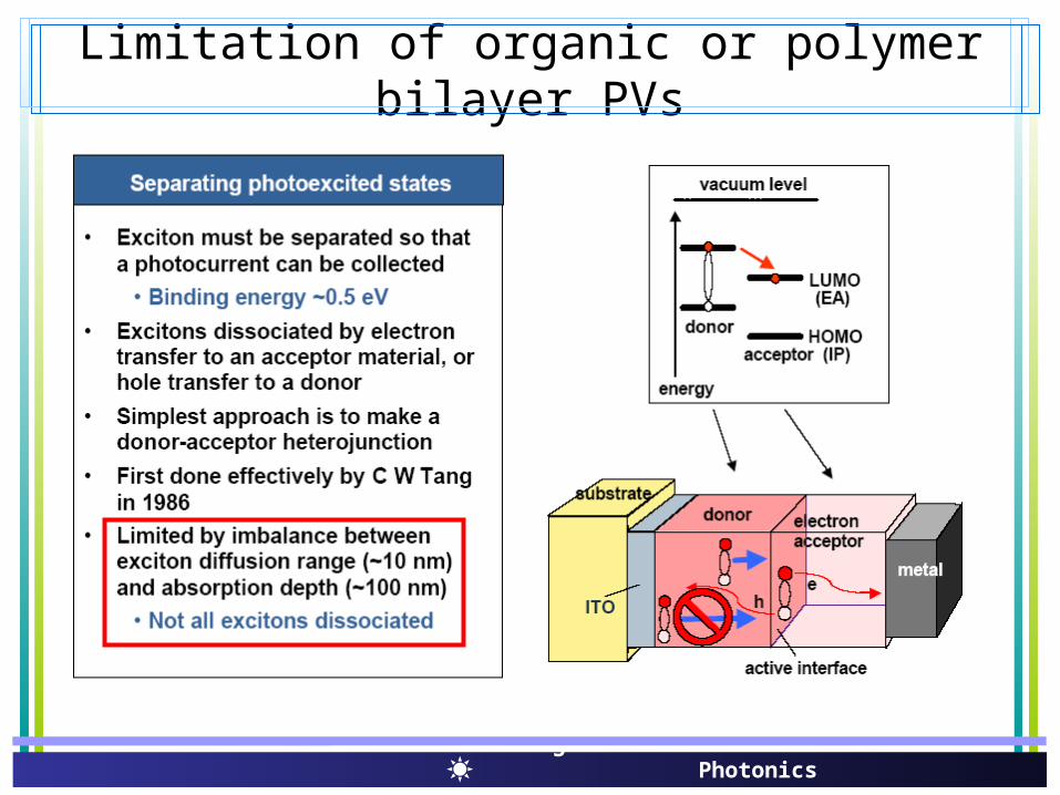
Exciton must be seperated so that a photocurrent can be collected.
Excitons dissociated by electron transfer to an acceptor material, or hole transfer to a donor.
Simplest approach is to make a donor-acceptor heterojunction
PV effect in conjugated polymer

Organic Materials for electronics & Photonics
Excitons dissociate at interfaces between materials having different ionization energies and electron affinities
Excitons are produced in a conducting polymer. An incident photon produces bound electron–hole pairs called excitons, which transport charges in photovoltaic polymers.
Exciton : generation & separation

Organic Materials for electronics & Photonics
Photo-induced charge transfer
donor
acceptor
anodecathode
AED
CT
CC
Photon absorption (A)
Exciton generation by absorption of light
Exciton diffusion (ED)
Exciton diffusion over ~LD (~20 nm)
Charge-transfer reaction (CT)
Exciton dissociation by rapid and efficient charge transfer
Collection of the carriers (CC)
Charge extraction by the internal electric field
EQE = AIQE = AEDCTCC
EQE: external quantum efficiency
IQE: internal quantum efficiency
Organic Materials for electronics & Photonics
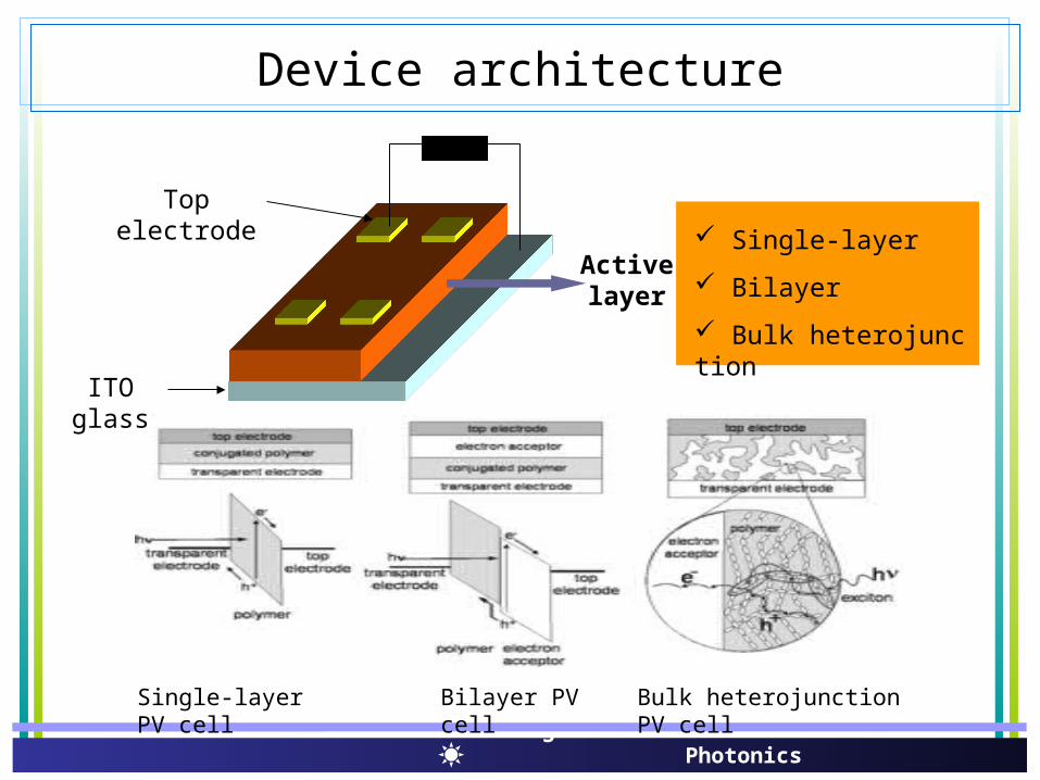
ITO glass
Top electrode
Active layer
Single-layer
Bilayer
Bulk heterojunction
Device architecture
Single-layer PV cell Bilayer PV cell Bulk heterojunction PV cell

Organic Materials for electronics & Photonics
I. Organic or polymer single-layer PVs
Disadvantage

Organic Materials for electronics & Photonics
Organic single crystals
Single-layer PVs

Organic Materials for electronics & Photonics
High exciton binding energy
Low bipolar mobility in one molecule
Limitation of single-layer PVs
Low efficiency

Organic Materials for electronics & Photonics
Charge transfer can occur between two semiconductors with offset energy levels. Excitons can diffuse approximately 10 nm to an interface. (less than 20 nm) A film thickness of approximately 100 nm is needed to absorb most of the light. Polymer bilayer cell showed 1.9 % energy conversion efficiency. Small molecule bilayer cell showed 3.6 % power conversion efficiency with 3 layers.
II. Organic or polymer bilayer PVs

Organic Materials for electronics & Photonics
Small molecular organic bilayer PV cell Improving molecular PV cell
Bilayer PVs
Organic Materials for electronics & Photonics
Limitation of organic or polymer bilayer PVs

Organic Materials for electronics & Photonics
III. Bulk heterojunction (BHJ) PVs

Organic Materials for electronics & Photonics
Device geometries

Organic Materials for electronics & Photonics
Working principle of BHJ device
1. Incoming photons are absorbed ⇒Creation of excitons on the Donor /Acceptor
2. Exciton is separated at the donor /acceptor interface Creation of charge carrier⇒s
3. Charge carriers within drift distance reach electrodes Creation of short circuit current I⇒ SC
1. The “photodoping” leads to splitting of Fermi levels Creation of open circuit voltage V⇒ OC
2. Charge transport properties, modulegeometry Fill factor FF⇒

Organic Materials for electronics & Photonics
Photoinduced charge generation

Organic Materials for electronics & Photonics
Charge transfer
Organic Materials for electronics & Photonics
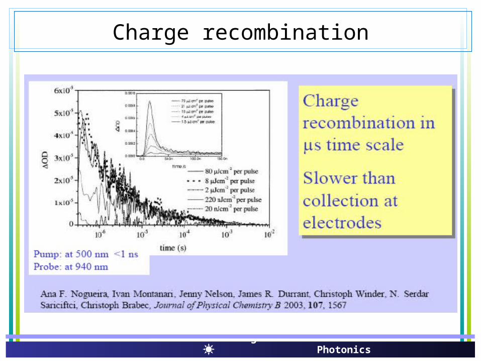
Charge recombination

Organic Materials for electronics & Photonics
3-D percolation
Organic Materials for electronics & Photonics
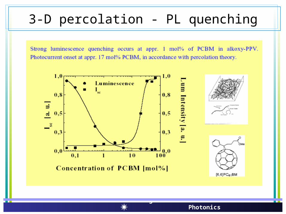
3-D percolation - PL quenching
Organic Materials for electronics & Photonics
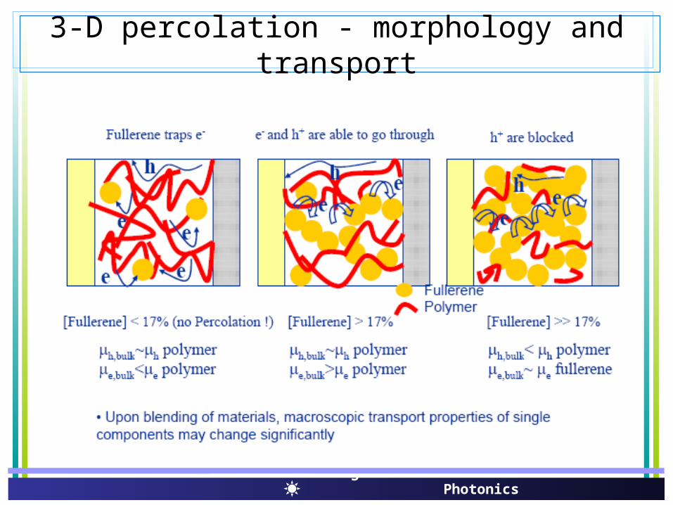
3-D percolation - morphology and transport
Organic Materials for electronics & Photonics
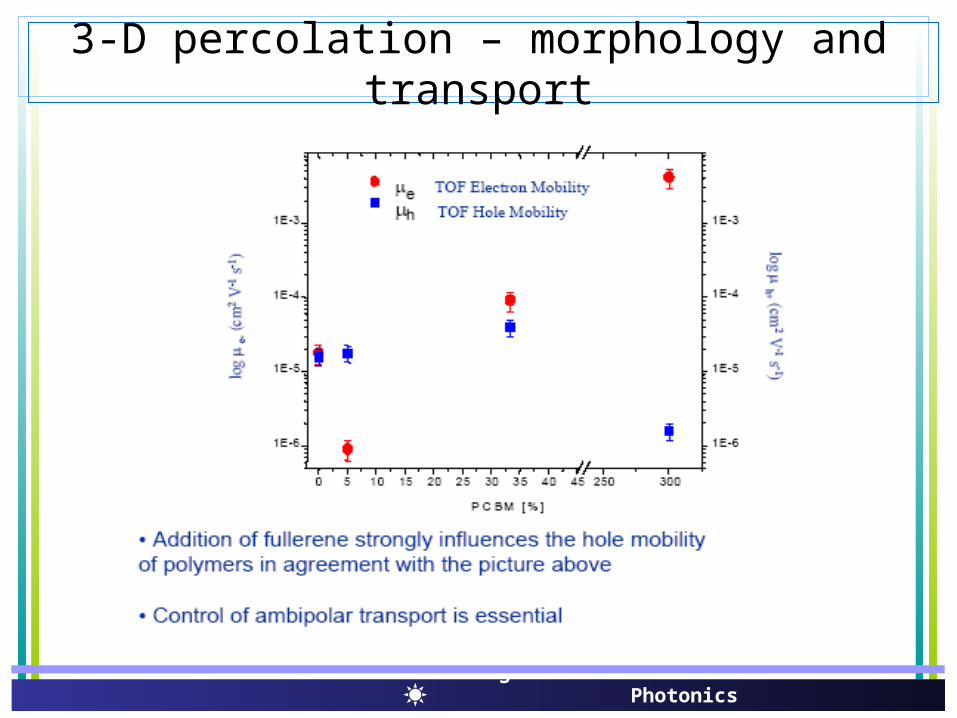
3-D percolation – morphology and transport

Organic Materials for electronics & Photonics
Efficiencies

Organic Materials for electronics & Photonics
Production

Organic Materials for electronics & Photonics
Film preparation

Organic Materials for electronics & Photonics
Film preparation

Organic Materials for electronics & Photonics
1. Conjugated polymer with low band gap
Maximum photon flux of sun = 700 nm
Eg= 1.24 / 0.7= 1.77 [eV]
Maximum absorption of photon of sun
2. Bulk heterojunction morphology
exciton diffusion length of conjugated polymer
= below 20 nm
3. High carrier mobility
electron and hole mobility of conjugated polymer
Isc: tuning of the transport property (mobility); Optimization of cell geometry in dependence of the cell thickness
Voc: tuning of the electronic energy level of the donor-acceptor system; Voc of ~2 V observed in polymeric donor- acceptor system
F.F: tuning of the contacts and morphology: lowering of serial resistance
Optimization for high efficiency
100S
ocsc
P
FFVI

Organic Materials for electronics & Photonics
donor acceptor
Polymer C60 derivative
Polymer Polymer
Polymer
CdSe nanocrystal
Polymer Metal oxide nanocrystal
Small molecule Small molecule
*
*
O
O
MDMO-PPV
OMe
O
PCBM
*S
*
P3HT
*
NS
N
*
F8BT
TiO2 or ZnO nanoparticles
CuPc
pentaceneN N **
PFB
Materials for BHJ organic solar cell
C60

Organic Materials for electronics & Photonics
*
*
O
O
OMe
O
MDMO-PPV PCBM
Donor/Acceptor composite solution
DA
Voc = 0.82 V
Jsc = 5.25 mA/cm2
FF = 0.61
AM1.5G = 2.5 % (under 80 mW/cm2)
< S. E. Shaheen, et al., Appl. Phys. Lett. 1998, 395, 257 >
glass
ITO
LiF
PEDOT:PSS
Active layer
Metal electrode
A. Polymer/PCBM interpenetrating system

Organic Materials for electronics & Photonics
Materials issue - matching the solar emission
The flexibility in chemical tailoring is necessary for matching the absorption of the PV material to the solar emission spectrum.
Organic Materials for electronics & Photonics
Bandgap engineering
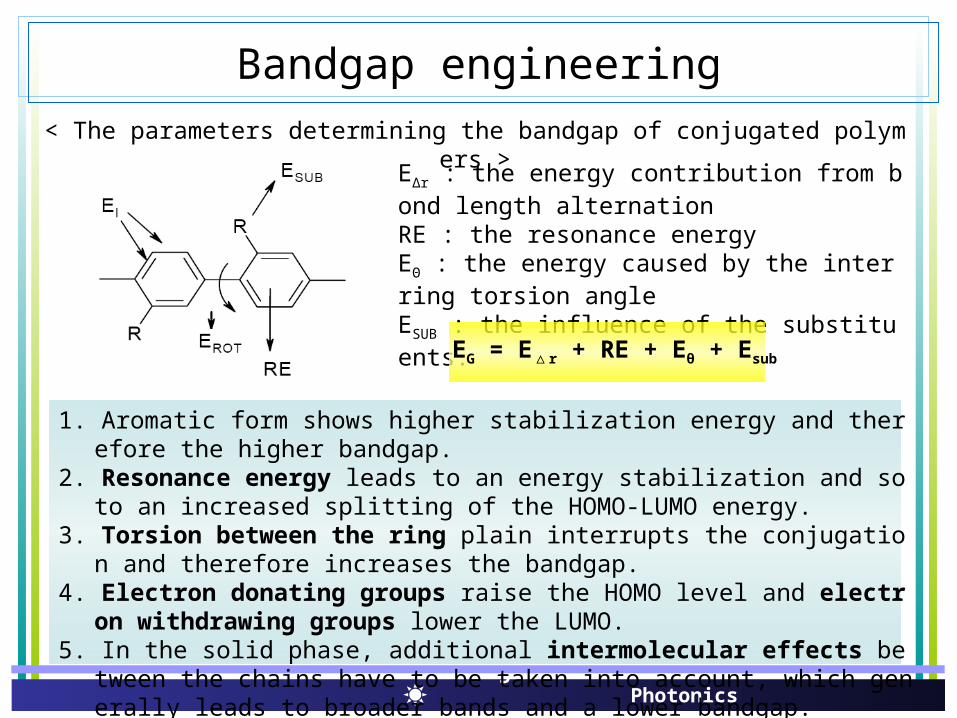
< The parameters determining the bandgap of conjugated polymers >
E∆r : the energy contribution from bond length alternation RE : the resonance energyEΘ : the energy caused by the inter ring torsion angle ESUB : the influence of the substituents.
EG = E r△ + RE + Eθ + Esub
1. Aromatic form shows higher stabilization energy and therefore the higher bandgap.2. Resonance energy leads to an energy stabilization and so to an increased splitting of t
he HOMO-LUMO energy.3. Torsion between the ring plain interrupts the conjugation and therefore increases the
bandgap.4. Electron donating groups raise the HOMO level and electron withdrawing groups
lower the LUMO.5. In the solid phase, additional intermolecular effects between the chains have to be ta
ken into account, which generally leads to broader bands and a lower bandgap.
Organic Materials for electronics & Photonics
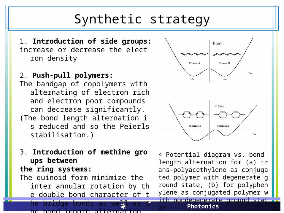
Synthetic strategy
1. Introduction of side groups:increase or decrease the electron density
2. Push-pull polymers:The bandgap of copolymers with alternating
of electron rich and electron poor compounds can decrease significantly.
(The bond length alternation is reduced and so the Peierls stabilisation.)
3. Introduction of methine groups betweenthe ring systems:The quinoid form minimize the inter annular
rotation by the double bond character of the bridge bonds as well as the bond length alternation .
(The structure becomes more flat and theresonance between the rings is increased.)
< Potential diagram vs. bond length alternation for (a) trans-polyacethylene as conjugated polymer with degenerate ground state; (b) for polyphenylene as conjugated polymer with nondegenerate ground state>
Organic Materials for electronics & Photonics
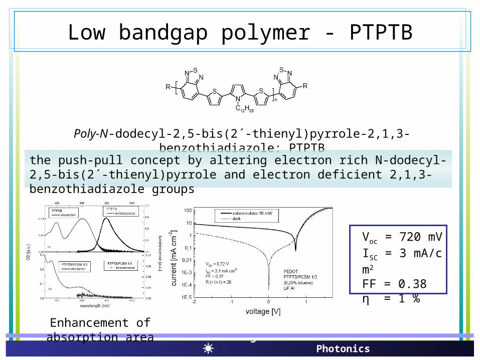
Poly-N-dodecyl-2,5-bis(2´-thienyl)pyrrole-2,1,3-benzothiadiazole: PTPTB
Voc = 720 mVISC = 3 mA/cm2
FF = 0.38η = 1 %
the push-pull concept by altering electron rich N-dodecyl-2,5-bis(2´-thienyl)pyrrole and electron deficient 2,1,3-benzothiadiazole groups
Low bandgap polymer - PTPTB
Enhancement of absorption area
Organic Materials for electronics & Photonics
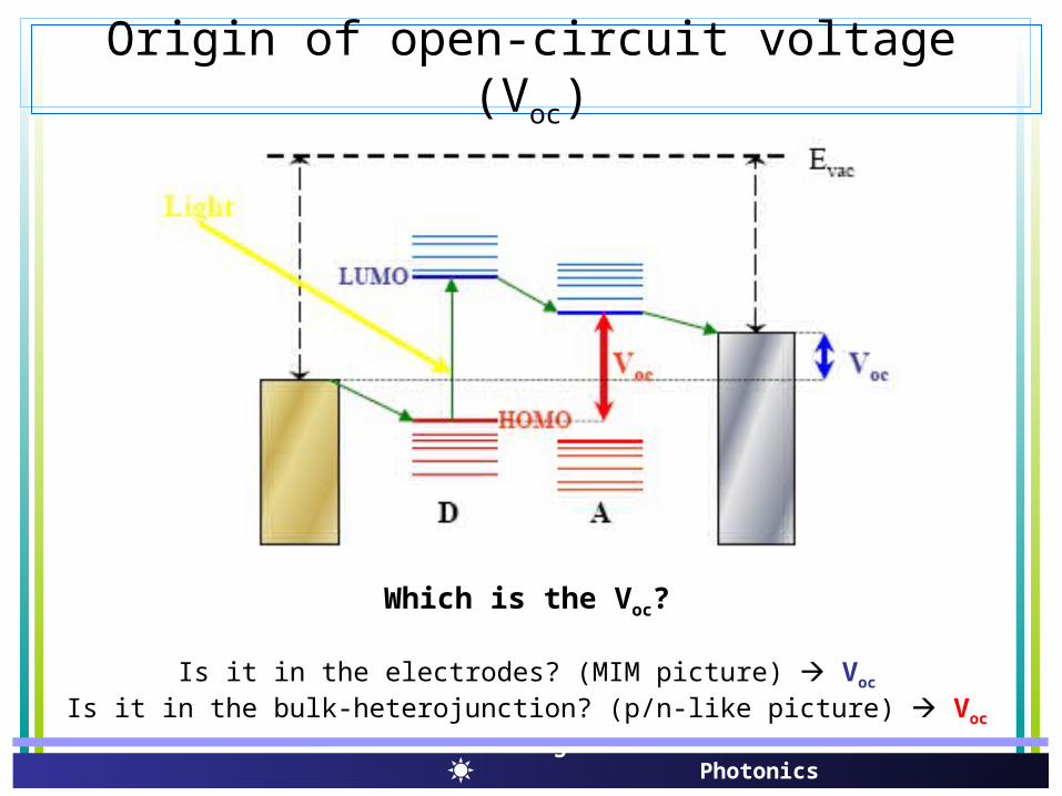
Which is the Voc?
Is it in the electrodes? (MIM picture) Voc
Is it in the bulk-heterojunction? (p/n-like picture) Voc
Origin of open-circuit voltage (Voc)

Organic Materials for electronics & Photonics
TOP ELECTRODE
WORK FUNCTION [eV]
Ca 2.87
Al 4.28
Ag 4.26
Au 5.1
S1 > S2
1. Voc in plastic solar cell is directly related to the acceptor strength of the fullerene.
2. The variation of negative electrode work function influences the Voc in only a minor way.
Variation of Voc

Organic Materials for electronics & Photonics
Optimization of contacts
LiF layers forms ohmic contact for electrons at the Al electrode:Contact resistivity limits FF.
Organic Materials for electronics & Photonics
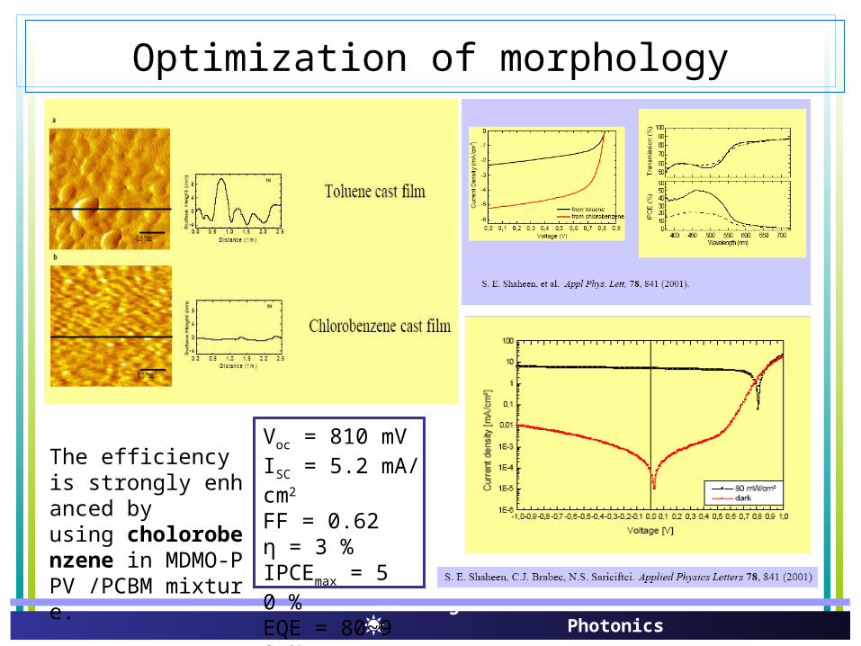
Optimization of morphology
Voc = 810 mVISC = 5.2 mA/cm2
FF = 0.62η = 3 %IPCEmax = 50 %EQE = 80~90 %
The efficiency is strongly enhanced byusing cholorobenzene in MDMO-PPV /PCBM mixture.

Organic Materials for electronics & Photonics
P3HT post production treatment: • increased absorption strength in the red• Higher conversion efficiency• Diode characteristics is improved
P3HT:PCBM “post production treatment”

Organic Materials for electronics & Photonics
Percolation problem in composites
Both donor and acceptor phases have to be percolated.

Organic Materials for electronics & Photonics
“Double Cable” polymers
Both donor and acceptor phases will be percolated at very low filling into a host polymer
Isc = 0.42 mA/cm2 Voc = 0.83 VFF = 0.29 (white light 88mW/cm2)

Organic Materials for electronics & Photonics
B. Hybrid polymer/nanoporous TiO2 system
• Almost all excitons can be split• No deadends• Polymer chains can be aligned
• Easy to model• Semiconductors can be changedwithout changing the geometry.
For efficient photoinduced charge generation
< Ideal device structure - ordered bulk heterojunctions >
TiO2 can be easily patterned into a continuous network for electron transport.
Organic Materials for electronics & Photonics
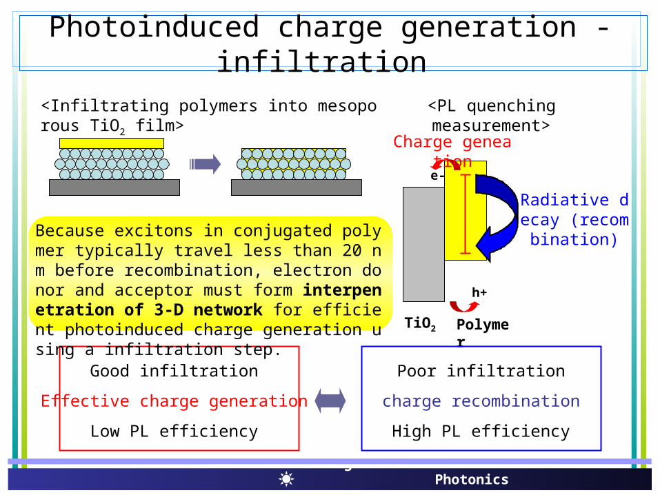
Photoinduced charge generation - infiltration
TiO2 Polymer
e-
h+
Radiative decay (recombination)
Charge geneation
Good infiltration
Effective charge generation
Low PL efficiency
Poor infiltration
charge recombination
High PL efficiency
<Infiltrating polymers into mesoporous TiO2 film>
Because excitons in conjugated polymer typically travel less than 20 nm before recombination, electron donor and acceptor must form interpenetration of 3-D network for efficient photoinduced charge generation using a infiltration step.
<PL quenching measurement>

Organic Materials for electronics & Photonics
< Melt infiltration step >
33 % of the volume of the film can be filled in several min.
< Mesoporous titania films >
P3HT/nanoporous TiO2 PV cell

Organic Materials for electronics & Photonics
Quantum dotCdSe Well defined photosensitivity large excition bohr radiu
s quantum confinement
7 nm by 7 nm 7 nm by 30 nm 7 nm by 60 nm
W.U. Huynh, J. Dittmer, A.P. Alivisatos Science, 295 (2002) 2425
C. Polymer/CdSe nanocrystal system
Power conversion efficiency: 1.7 %

Organic Materials for electronics & Photonics
D. Small molecular weight organic system< Small molecular organic semiconductor materials >

Organic Materials for electronics & Photonics
C. W. Tang’s Heterojunction Solar Cell• first heterojunction for efficient charge generation• ~0.95% conversion efficiency• nearly ideal IVs (FF~0.65)• under full solar illumination (1 sun)
• Photoluminescence (PL) probes the exciton lifetime• Exciton lifetime depends on proximity of donor acceptor interface
CuPc/PTCBI device

Organic Materials for electronics & Photonics
Double heterojunction
• cathode metal diffusion• deposition damage• exciton-plasmon interaction• vanishing optical field• electrical shorts
Introduce ‘Exciton Blocking Layer’ (EBL) to:• confine excitons to active region• act as a damage-absorber

Organic Materials for electronics & Photonics
Exciton blocking layer
Exciton Blocking Layer (EBL)Improves thin cell efficiency

Organic Materials for electronics & Photonics
E. Laminated polymeric system
DA
**S
*NC
*
O
O
POPT rich MEH-CN-PPV rich
ITO or PEDOT on gold
glassAl or Ca
laminated fabrication
anealing200 oC
Au/PEDOT/ POPT:MEH-CN-PPV (19:1) laminated at 200 C onto theMEH-CN-PPV:POPT (19:1) /Ca
Power conversion efficiency around 4.8 % at 480nm irradiation.Calculated AM1.5 efficiency around 1.9 %
Large scale large area fabrication potential
M. Granström, K. Petritsch, A. Arias, A. Lux,
M. Andersson and R. H. Friend,Nature 395, 257 (1998)
Organic Materials for electronics & Photonics
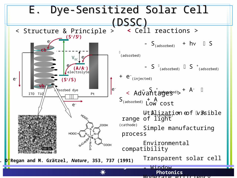
< Advantages >
Low cost
Utilization of visible range of light
Simple manufacturing process
Environmental compatibility
Transparent solar cell
- Window
Moderate efficiency ~10%
ITO TiO2 PtAdsorbed dye
electrolyte(A/A-)
(S+/S)
vb
cb
(S+/S)
e-
e-
e-
e-
e-
e-VOC
< Cell reactions >
- S(adsorbed) + h S (adsorbed)
- S (adsorbed) S +(adsorbed) + e-
(injected)
- S +(adsorbed) + A- S(adsorbed) + A
- A(cathode) + e- A-(cathode)
< Structure & Principle >
B. O’Regan and M. Grätzel, Nature, 353, 737 (1991)
E.E. Dye-Sensitized Solar Cell (DSSC)Dye-Sensitized Solar Cell (DSSC)
Organic Materials for electronics & Photonics
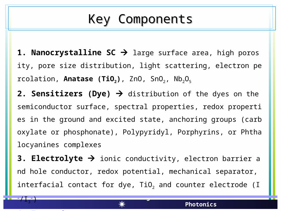
1. Nanocrystalline SC large surface area, high porosity, pore size distribution, l
ight scattering, electron percolation, Anatase (TiO2), ZnO, SnO2, Nb2O5
2. Sensitizers (Dye) distribution of the dyes on the semiconductor surface, spect
ral properties, redox properties in the ground and excited state, anchoring groups (carb
oxylate or phosphonate), Polypyridyl, Porphyrins, or Phthalocyanines complexes
3. Electrolyte ionic conductivity, electron barrier and hole conductor, redox pote
ntial, mechanical separator, interfacial contact for dye, TiO2 and counter electrode (I–/I
3–)
4. Extra transparent conductive oxide (conductivity, transmittance), sealing, meta
l grid, counter electrode
Key ComponentsKey Components

Organic Materials for electronics & Photonics
(1) Excitation of dye under illumination (ns)
(2) Electron injection (ps)
(3) Electron transport (ms)
(4) Regeneration of dye (10 ns)
(5) Recombination with oxidized redox (ms)
(6) Recombination with oxidized dye (s)
30 mM of I– is enough to reduce the most of dye cations
I. Montanari et al., J. Phys. Chem. B, 106, 12203 (2002)
Dynamics Dynamics

Organic Materials for electronics & Photonics
Power curve (I-V curve)
0.0 0.1 0.2 0.3 0.4 0.5 0.6 0.70
1
2
3
4
5
6
7
8
9
10
J (m
A/c
m2 )
Voltage (V)
Jsc
Voc
FF
Jsc: Diffusion coefficient (Length) H+ or Li+ cation on TiO2
TiCl4 acidic sol. Treatment Increase in adsorbed dye
Voc: Electron lifetime (Recombination) TBP, Ammonia in electrolyte Secondary oxide layer
FF: Series and Shunt Resistance (Recombination) Secondary oxide layer
To increase performance of DSSC
Competition between Jsc and Voc: High carrier High probability of recombination
= Pr
Pmax =Pr
FF IscVoc
Current issuesCurrent issues
Organic Materials for electronics & Photonics
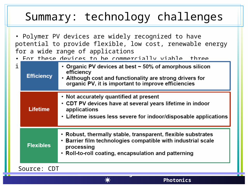
• Polymer PV devices are widely recognized to have potential to provide flexible, low cost, renewable energy for a wide range of applications• For these devices to be commercially viable, three important areas must be addressed
Source: CDT
Summary: technology challenges

Organic Materials for electronics & Photonics
Materials• Up to now, polymers for PVs have largely been taken from the LEP program• Work underway at CDT to develop new polymers optimized to absorb solar radiation• Materials optimized for electron or holetransport
Device Architecture• Morphology of polymer blend crucial to determining device performance• Morphology can be controlled through careful processing, surface treatment and materials design• Many advances in LEP architecture are applicable to PV device development
Source: CDT
Summary: optimization
Organic Materials for electronics & Photonics
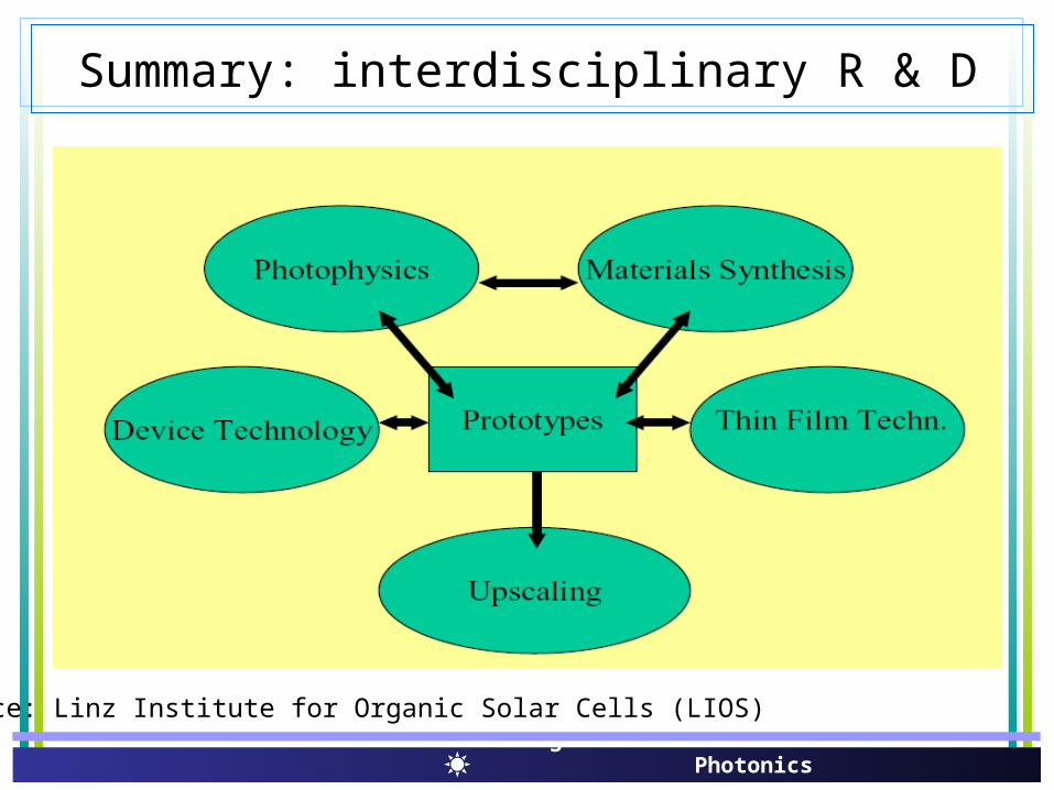
Source: Linz Institute for Organic Solar Cells (LIOS)
Summary: interdisciplinary R & D