SOLUTION PROCESSED ORGANIC SEMICONDUCTOR THIN-FILM ...zc714wk4534/Stanford PhD... · semiconductor...
166
SOLUTION PROCESSED ORGANIC SEMICONDUCTOR THIN-FILM TRANSISTORS FOR FLEXIBLE ELECTRONICS: DEVICE PHYSICS, DEVICE MODELING, FABRICATION TECHNOLOGY, AND INTERFACE ENGINEERING A DISSERTATION SUBMITTED TO THE DEPARTMENT OF ELECTRICAL ENGINEERING AND THE COMMITTEE ON GRADUATE STUDIES OF STANFORD UNIVERSITY IN PARTIAL FULFILLMENT OF THE REQUIREMENTS FOR THE DEGREE OF DOCTOR OF PHILOSOPHY Zihong (Bill) Liu November 2009 [Defense Date: September 10 th , 2009]
Transcript of SOLUTION PROCESSED ORGANIC SEMICONDUCTOR THIN-FILM ...zc714wk4534/Stanford PhD... · semiconductor...
SOLUTION PROCESSED ORGANIC SEMICONDUCTOR
THIN-FILM TRANSISTORS FOR FLEXIBLE ELECTRONICS:
DEVICE PHYSICS, DEVICE MODELING, FABRICATION
TECHNOLOGY, AND INTERFACE ENGINEERING
A DISSERTATION
SUBMITTED TO THE DEPARTMENT OF ELECTRICAL ENGINEERING
AND THE COMMITTEE ON GRADUATE STUDIES
OF STANFORD UNIVERSITY
IN PARTIAL FULFILLMENT OF THE REQUIREMENTS
FOR THE DEGREE OF
DOCTOR OF PHILOSOPHY
Zihong (Bill) Liu
November 2009
[Defense Date: September 10th, 2009]
http://creativecommons.org/licenses/by-nc/3.0/us/
This dissertation is online at: http://purl.stanford.edu/zc714wk4534
© 2010 by Zihong Liu. All Rights Reserved.
Re-distributed by Stanford University under license with the author.
This work is licensed under a Creative Commons Attribution-Noncommercial 3.0 United States License.
ii
I certify that I have read this dissertation and that, in my opinion, it is fully adequatein scope and quality as a dissertation for the degree of Doctor of Philosophy.
Yoshio Nishi, Primary Adviser
I certify that I have read this dissertation and that, in my opinion, it is fully adequatein scope and quality as a dissertation for the degree of Doctor of Philosophy.
Zhenan Bao
I certify that I have read this dissertation and that, in my opinion, it is fully adequatein scope and quality as a dissertation for the degree of Doctor of Philosophy.
Krishna Saraswat
Approved for the Stanford University Committee on Graduate Studies.
Patricia J. Gumport, Vice Provost Graduate Education
This signature page was generated electronically upon submission of this dissertation in electronic format. An original signed hard copy of the signature page is on file inUniversity Archives.
iii
iv
Abstract
Organic or carbon electronics has been a fast-growing field in recent years covering a
broad range from nanoelectronic devices to macroelectronic systems. Besides the single-
graphene or single-carbon nanotube transistor toward extending the scaling limit of
traditional silicon metal-oxide-semiconductor field-effect transistor (MOSFET), organic
semiconductor based thin-film transistors have been actively investigated due to their
promise in large-area electronics fabricated on flexible substrates using low-cost
unconventional means, such as low/room-temperature printing and roll-to-roll
processing. This dissertation focuses on the study of device physics, device modeling,
fabrication technology, and interface engineering for solution-processed organic field-
effect transistors (SPOFET) for flexible electronics applications. There are primarily
four parts of contributions originated from this dissertation work.
The first part introduces the design and demonstration of high-performance, low-
voltage flexible SPOFETs fabricated on plastic substrates with a carrier mobility over
0.2 cm2/Vs, a turn-on voltage of near 0 V, and a record low subthreshold slope of ~80
mV/dec in ambient conditions. These exceptional characteristics are achieved by novel
device architecture design, 3-D statistical modeling for solution-shearing process
optimization, and phenyl-terminated self-assembled monolayer (SAM) based interface
engineering.
In the second part, SAM relevant physical effects and chemistry effects at the
organic semiconductor-dielectric interface are systematically investigated. Through
careful selection of a group of phenyl-terminated SAMs, we elucidate how the
performance and reliability of organic transistors are controlled by the critical
semiconductor-dielectric interfacial SAMs. In addition, we briefly introduce a spin-
v
coating process for depositing high-quality phenyl-terminated SAMs for organic
electronics applications.
The third part focuses on the device physics and device modeling of organic
transistors. In this dissertation work, we have proposed and developed a universal
physical model for organic transistors by incorporating both the charge injection effects
and charge transport properties, and successfully applied it to resolve many elusive
physical phenomena observed so far, such as the peculiar mobility scaling behavior with
respect to the channel length, the contact resistance effect, and the mysterious surface
potential profiles of organic transistors which have been experimentally probed yet
poorly understood. Of particular importance is that we discover an overshoot region in
the mobility scaling behavior and identified the existence of a critical channel length for
the peak field-effect mobility.
In the last part, we investigate novel contact engineering for organic transistors
toward lowering charge injection barrier and reducing the interfacial disorder width or
localization states. We have explored and demonstrated Fermi-level depinning at the
metal-organic interface for low-resistance Ohmic contacts by inserting an ultrathin
interfacial Si3N4 insulator in between. The contact behavior is successfully tuned from
rectifying to quasi-Ohmic and to tunneling by varying the Si3N4 thickness within 0-6 nm.
Detailed physical mechanisms of Fermi-level pinning/depinning responsible for the
metal-organic semiconductor contact behavior are clarified based on a proposed
lumped-dipole model.

vi
vii
To My Family Who Raised Me Up in the World of Humanity
To My Teachers Who Raised Me Up in the World of Science

viii
ix
Acknowledgments
This journey would not have been possible without the support, guidance, inspiration
and encouragement from many people to whom I am deeply and forever indebted.
First of all, I would like to extend my heartfelt gratitude to my supervisors, Professor
Yoshio Nishi in the Department of Electrical Engineering and Professor Zhenan Bao in
the Department of Chemical Engineering, who both have been rigorously advising,
strongly supporting, and generously helping me throughout my graduate studies and
research. Imagining working in both electrical engineering and chemical engineering as
handily as I do today would never come true without extraordinary guidance and
support from both of my supervisors in the two distinctive departments. Professor
Yoshio Nishi has over forty years of research and management experience in the
semiconductor industry and academia. His broad intelligence and unique insight to the
semiconductor technology have been a constant source of inspiration and
encouragement to my graduate research as well as future career. In addition, his well-
respected leadership and personality deeply influence me and set an example for us
students. Professor Zhenan Bao is a well-known expert in the field of organic
electronics and has made revolutionary contributions to the development of high
performance organic semiconductor materials and devices. Her keen sense of
experiments, grand ambitiousness of scientific research and enduring patience provided
me invaluable help to thrive in the emerging field of nano-/macro-electronics. I also
appreciate both supervisors for guiding me how to develop to a true research scientist.
I am also grateful to Professor Alberto Salleo and Professor Krishna Saraswat for
their valuable suggestions on the research and for their precious time and efforts as
members of my reading and defense committee.
x
Over the past three years of my PhD studies and research at Stanford University,
there have been constant valuable interactions and collaboration with members from
various groups focusing on semiconductor devices, organic electronics, and
nanotechnology, including Dr. Hector Becerril, Dr. Mark Roberts, Dr. Peng Wei, Dr.
Liangbing Hu, Dr. Eric Verploegen, Ajay Virkar, Dr. Toshifumi Irisawa, Dr. Joon Hak
Oh, Dr. Blanka Magyari-Kope, and Dr. Masaharu Kobayashi. I appreciate their
tremendous help and great collaboration that made this work possible. In addition, I
would like to thank Professor Yoshio Nishi’s entire group and Professor Zhenan Bao’s
entire group where numerous colleagues offered support and help along with my
research in the labs.
Special thanks go to the Toshiba Inc. who has been sponsoring this project through
Stanford CIS-FMA program. Particularly, Dr. Bipul Paul and Dr. Masaki Okajima have
been providing suggestions and discussions as the CIS-FMA project mentors, and I
appreciate their support and contributions to the success of this project.
Also, I wish to take this opportunity to extend my sincere thanks to all of my
teachers from kindergarten to graduate school who have truly raised me up in the world
of science, step by step and word by word.
Research is tough. Failures and frustrations always come along the way to the
ultimate success. I can not sustain it without mental well-being and spiritual support,
most importantly, from my family. I am indebted to my parents, my three elder sisters,
and my girlfriend for their never-fading and purely selfless love, support, encouragement
and prayers throughout my whole life. I will try my best to spend the rest of my life
making them as happy as they have made me.
xi
Contents
Abstract..................................................................................................... iv
Acknowledgments .................................................................................... ix
List of Tables........................................................................................... xv
List of Figures ....................................................................................... xvii
1 Introduction ........................................................................................... 1
1.1 Historical Overview of Semiconductor Electronics ............................................2
1.2 Carbon Materials for Nano- and Macro-Electronics ...........................................3
1.3 Motivations and Objectives .....................................................................................5
1.4 Organization of this Dissertation............................................................................9
2 High-Performance Solution Processed Flexible Organic Transistor .. 11
2.1 Flexible SPOFET Device: Design and Fabrication .......................................... 13
2.1.1 4T-TMS Electronic Properties ............................................................................. 15
2.1.2 4T-TMS SPOFET on Silicon Substrate.............................................................. 17
2.1.3 Comparison of Different Solution Deposition Methods................................. 22
2.1.4 3-D Statistical Process Optimization................................................................... 22
2.1.5 Optimized SPOFET Performance on Silicon Substrate .................................. 33
xii
2.2 Flexible SPOFET Device: Performance and Discussion ................................. 38
2.3 Summary .................................................................................................................. 43
3 Interface Engineering by Self-Assembled Monolayer......................... 45
3.1 Background and Motivation ................................................................................. 45
3.2 Phenyl-SAM Processing and Characterization................................................... 49
3.2.1 Spin-coating Process and Mechanism ................................................................. 49
3.2.2 Spin-coated Phenyl-SAM Characterization......................................................... 52
3.3 Phenyl-SAM Effects in Organic Transistors ...................................................... 55
3.3.1 PBTTT Transistor Structure and Device Fabrication....................................... 55
3.3.2 Device Electrical Characteristics .......................................................................... 56
3.3.3 Threshold Voltage Control by SAM Dipole Moment ...................................... 61
3.4 Summary .................................................................................................................. 66
4 Device Physics and Universal Modeling of Organic Transistor ......... 67
4.1 Background and Motivation ................................................................................. 68
4.2 Universal Modeling of Organic Transistors ....................................................... 70
4.2.1 Charge Injection at the Metal-Organic Interface ............................................... 72
4.2.2 Charge Transport in the Active Layer: EPME Model ...................................... 78
4.2.3 Unified Model for Transistor Operations........................................................... 84
4.3 Simulation vs. Experimental Results.................................................................... 88
4.3.1 Transfer and Output Characteristics.................................................................... 89
4.3.2 Surface Potential Profile and Contact Resistance .............................................. 92
4.3.3 Mobility Scaling Behavior...................................................................................... 95
4.4 Summary .................................................................................................................. 99
xiii
5 Contact Engineering for Organic Electronic Device ......................... 101
5.1 Background ........................................................................................................... 101
5.2 Experimental Results on Fermi-Level Depinning........................................... 102
5.3 Theory and Proposed Model .............................................................................. 109
5.4 Summary ................................................................................................................ 114
6 Conclusions and Outlook ................................................................... 117
6.1 Conclusions ........................................................................................................... 117
6.2 Outlook.................................................................................................................. 119
Appendix A. Spin-coating Process for Phenyl-Terminated Self-
Assembled Monolayer ............................................................................ 121
Bibliography ........................................................................................... 125

xiv
xv
List of Tables
Table 2.1 Experiment design of the first 24 different processing conditions
(“BL-1”) toward systematic study and optimization of the shearing process.......24
Table 3.1 SAM molecule dipole, molecule length, and SAM density as simulated
using Gaussian package and PM3/MOPAC9 model. ..............................................64
Table 4.1 Representative parameters, corresponding physical meaning and
typical value used for the simulation based on the universal device model in this
work .................................................................................................................................88

xvi
xvii
List of Figures
Figure 1.1 The historical development of traditional silicon metal-oxide-
semiconductor field-effect transistors (MOSFET) used for VLSI circuits. Source
data: Intel and ITRS.........................................................................................................3
Figure 1.2 Schematic structure of a typical (a) bottom-gate, top-contact and
(b)bottom-gate, bottom-contact organic TFT. S: source, D: drain, G: gate. ..........5
Figure 1.3 A proposed roll-to-roll manufacturing process for solution processed
organic thin-film transistors. ..........................................................................................6
Figure 1.4 A historical overview of the organic transistor performance based on
different materials and processes. Adapted from [18]. Copyright © 2005 IEEE. .7
Figure 2.1 Illustration of the subthreshold slope (SS), as defined by
∂(logIDS)/∂VGS, which reflects how fast the transistor is switched between the on
and off state. ...................................................................................................................12
Figure 2.2 (a) Device structure and (b) photograph of our flexible 4T-TMS
SPOFETs. (c) Scanning electron microscopy (SEM) image of the bilayer PVP-
EAD dielectric that possesses apparent single-layer morphology. SEM was
performed at 3 keV in a tilt angle of 45º on an deliberately peeled-off area to
examine both the surface and the cross section. .......................................................14
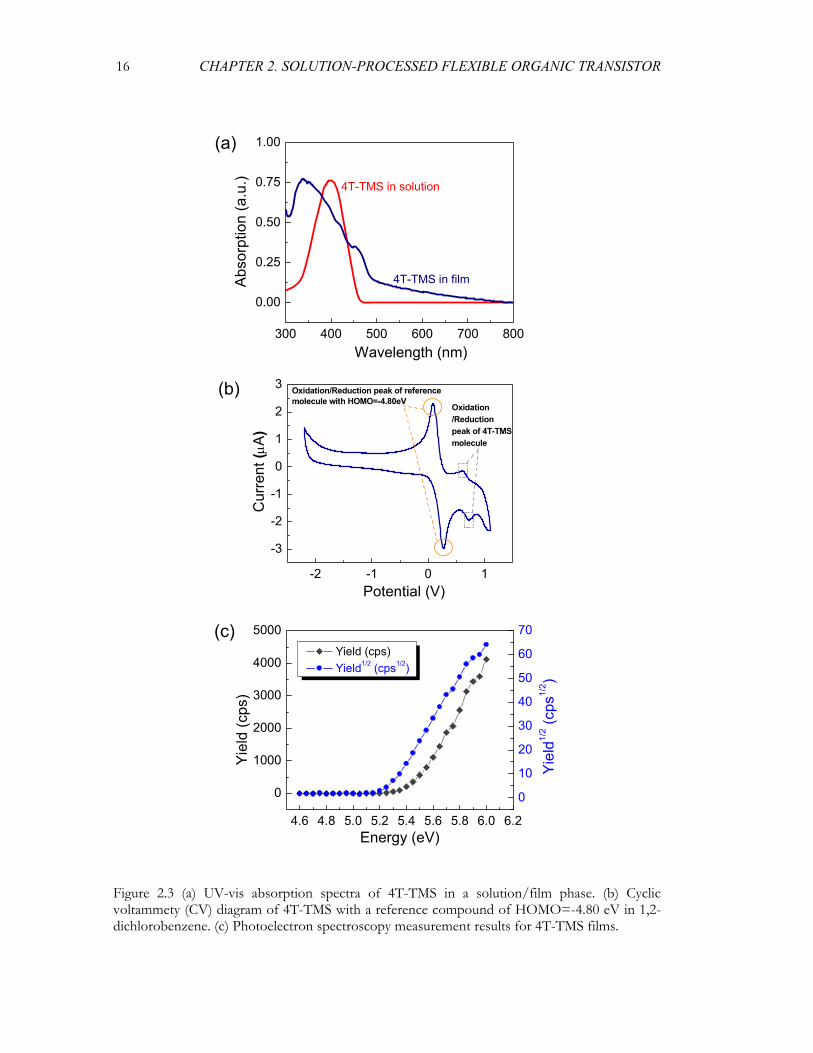
Figure 2.3 (a) UV-vis absorption spectra of 4T-TMS in a solution/film phase. (b)
Cyclic voltammety (CV) diagram of 4T-TMS with a reference compound of
HOMO=-4.80 eV in 1,2-dichlorobenzene. (c) Photoelectron spectroscopy
measurement results for 4T-TMS films......................................................................16
xviii
Figure 2.4 SPOFET device structure on silicon substrate and its basic fabrication
process flow. .................................................................................................................. 18
Figure 2.5 Surface structure, water contact angle and cross-polarized microscope
image of 4T-TMS film deposited by solution shearing process on (a) PTS treated
substrate and (b) OTS treated substrate. Large crystalline domain films can be
successfully deposited on PTS substrate, while nonuniform or little film is
consistently observed on OTS substrate due to its dewettability to the 4T-TMS
organic semiconductor solutions. ............................................................................... 19
Figure 2.6 Illustration of the solution shearing process and analysis of the
shearing forces during the film growth. ..................................................................... 20
Figure 2.7 Simplified energy band diagrams without considering interface dipole
effect for the top-contact 4T-TMS SPOFET on silicon substrate along (a)
source-to-drain channel direction and (b) gate-to-film direction. The
HOMO/LUMO levels are based on the measurement as described in Section
2.1.1. ................................................................................................................................ 21
Figure 2.8 Cross-polarized optical micrographs of the 4T-TMS thin films
deposited by (a)-(b) spin-coating method, from 5 mg/mL solution in
chlorobenzene at (a) room temperature or (b) elevated temperature of ~80ºC;
(c)-(d) drop casting method (c) with or (d) without solvent annealing; (e)-(f)
solution shearing method with (e) 4T-TMS solution concentration: 6 mg/mL in
xylene, deposition temperature: 112 ºC, shearing speed: 0.10 mm/s and (f) 4T-
TMS solution concentration: 6 mg/mL in chlorobenzene, deposition
temperature: 78.6 ºC, shearing speed: 0.10 mm/s. (g) AFM tapping-mode height
image of a local film shown in (e). .............................................................................. 23
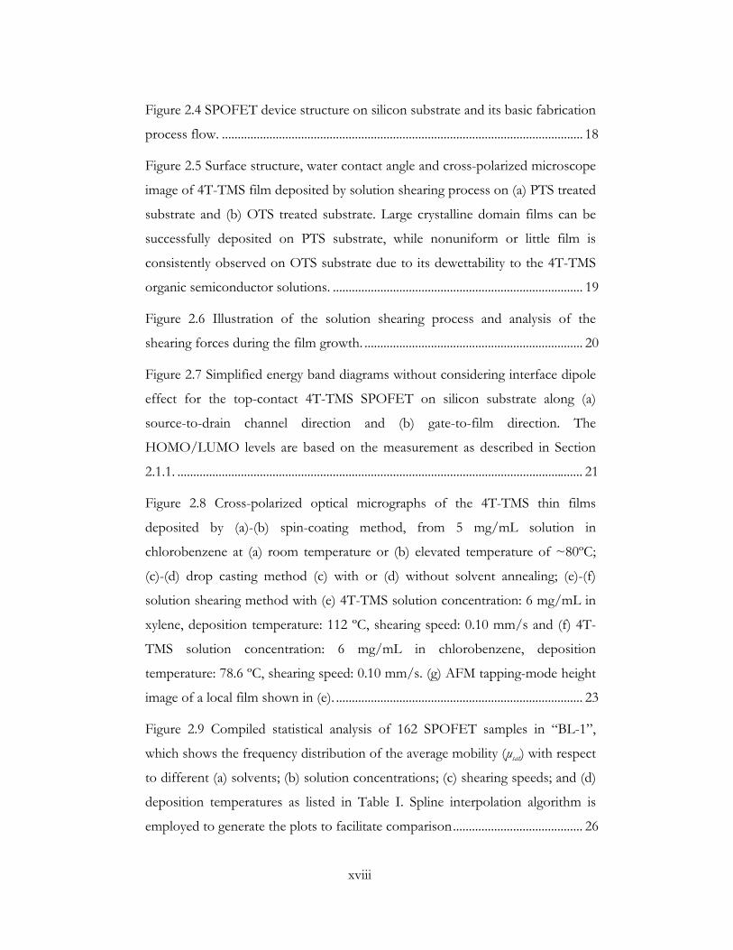
Figure 2.9 Compiled statistical analysis of 162 SPOFET samples in “BL-1”,
which shows the frequency distribution of the average mobility (μsat) with respect
to different (a) solvents; (b) solution concentrations; (c) shearing speeds; and (d)
deposition temperatures as listed in Table I. Spline interpolation algorithm is
employed to generate the plots to facilitate comparison......................................... 26
xix
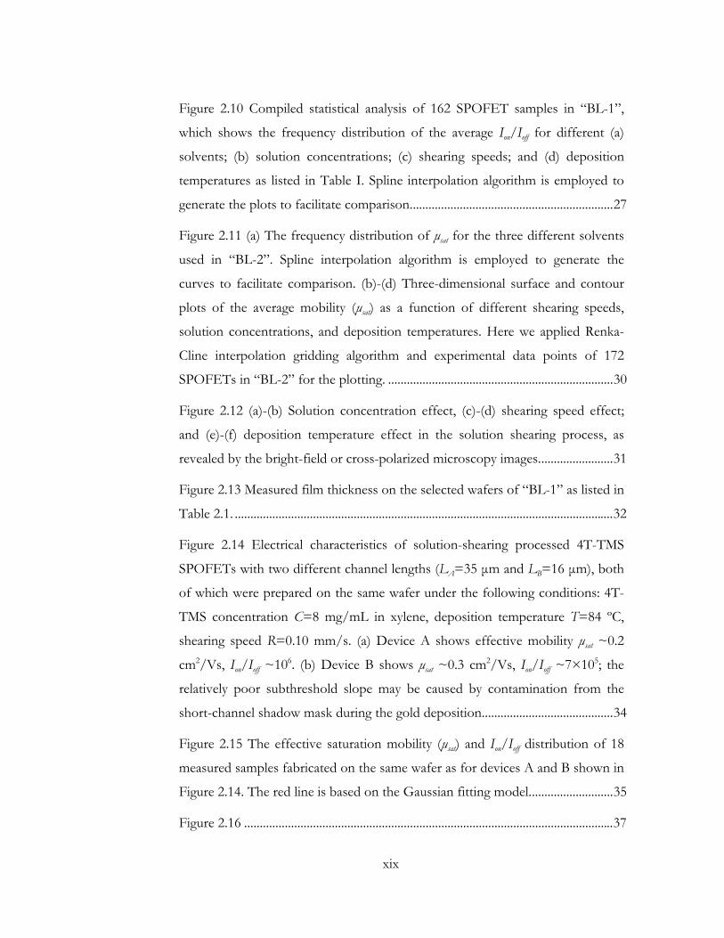
Figure 2.10 Compiled statistical analysis of 162 SPOFET samples in “BL-1”,
which shows the frequency distribution of the average Ion/Ioff for different (a)
solvents; (b) solution concentrations; (c) shearing speeds; and (d) deposition
temperatures as listed in Table I. Spline interpolation algorithm is employed to
generate the plots to facilitate comparison.................................................................27
Figure 2.11 (a) The frequency distribution of μsat for the three different solvents
used in “BL-2”. Spline interpolation algorithm is employed to generate the
curves to facilitate comparison. (b)-(d) Three-dimensional surface and contour
plots of the average mobility (μsat) as a function of different shearing speeds,
solution concentrations, and deposition temperatures. Here we applied Renka-
Cline interpolation gridding algorithm and experimental data points of 172
SPOFETs in “BL-2” for the plotting. ........................................................................30
Figure 2.12 (a)-(b) Solution concentration effect, (c)-(d) shearing speed effect;
and (e)-(f) deposition temperature effect in the solution shearing process, as
revealed by the bright-field or cross-polarized microscopy images........................31
Figure 2.13 Measured film thickness on the selected wafers of “BL-1” as listed in
Table 2.1. .........................................................................................................................32
Figure 2.14 Electrical characteristics of solution-shearing processed 4T-TMS
SPOFETs with two different channel lengths (LA=35 μm and LB=16 μm), both
of which were prepared on the same wafer under the following conditions: 4T-
TMS concentration C=8 mg/mL in xylene, deposition temperature T=84 ºC,
shearing speed R=0.10 mm/s. (a) Device A shows effective mobility μsat ~0.2
cm2/Vs, Ion/Ioff ~106. (b) Device B shows μsat ~0.3 cm2/Vs, Ion/Ioff ~7×10⁵; the
relatively poor subthreshold slope may be caused by contamination from the
short-channel shadow mask during the gold deposition..........................................34
Figure 2.15 The effective saturation mobility (μsat) and Ion/Ioff distribution of 18
measured samples fabricated on the same wafer as for devices A and B shown in
Figure 2.14. The red line is based on the Gaussian fitting model...........................35
Figure 2.16 ......................................................................................................................37
xx
Figure 2.17 Out-of-plane X-ray diffraction (XRD) spectra of solution-sheared
4T-TMS thin film. The inset is a cross-polarized optical microscopy image of the
highly crystalline film on plastic PET substrate........................................................ 39
Figure 2.18 (a) Transfer [Vds=-1.5 V] and (b) output characteristics of the
flexible 4T-TMS SPOFETs. (c) A simplified energy band diagram clarifying the
device physics responsible for the ideal turn-on voltage. (d) Device performance
with respect to different operating voltages. ............................................................. 40
Figure 2.19 A review on the representative flexible SPOFET performances
(except [54] which is based on vapor process) reported in literature in the past
decade. Our work contributes to one of the highest performances, with a
record-low subthreshold slope of ~80 mV/dec....................................................... 42
Figure 3.1 Schematic illustration of the gate voltage induced charge carrier layer,
which is close to the semiconductor-dielectric interface. ........................................ 46
Figure 3.2 Schematic illustration of the concept of dielectric surface modification
by self-assembled monolayers. .................................................................................... 47
Figure 3.3 A group of phenyl-terminated SAM molecules used for the interface
engineering study in this work. The intra alkyl chain length increases from PTS,
PETS, PBTS, to PHTS, PAPTS is comparable to PBTS except that an –NH-
group replaces a –CH2- in the intra part of PBTS. (PTS: phenyltrichlorosilane,
PETS: phenethyltrichlorosilane, PBTS: 4-phenylbutyltrichlorosilane, PHTS: 6-
phenylhexyltrichlorosilane, PAPTS: N-phenylaminopropyltricholorosilane) ...... 48
Figure 3.4 Schematic illustration of the spin-coating process for depositing
phenyl-terminated SAMs from the solution of phenyl-trichlorosilane in
anhydrous toluene. The trichlorosilane headgroup spontaneously aggregate and
align on the liquid drop surface, providing an ideal environment for the fast
reaction of the trichlorosilane with the hydroxyl group on the substrate surface
[70-71]. The anhydrous toluene solvent being selected here is critical to the
xxi
process. The conjugated aromatic group of toluene is supposed to interact with
the functional endgroup of the phenyl-silane and facilitate the alignment of the
phenyl-silane on the liquid drop surface.....................................................................51
Figure 3.5 A preliminary screening of different film morphology as deposited by
different spin-coating processes for PBTS. Images were taken under bright-field
microscope. The solvent, concentration and spin rate/time are all critical to high
quality phenyl-SAM. ......................................................................................................51
Figure 3.6 Measured water contact angle on phenyl-SAM modified SiO2
surfaces. The molecular length of each SAM molecule is computed by
PM3/MOPAC9 model and shown for comparison purpose here.........................53
Figure 3.7 Representative phenyl-SAM film morphology for (a)
PTS/PETS/PBTS/PHTS and (b) PAPTS, as deposited by the optimized spin-
coating process. For PTS-series SAM, the typical roughness is 0.1-0.2 nm (rms);
for PAPTS SAM, the roughness is 0.2-0.3 nm (rms). This indicates the spin
coating process yields excellent phenyl-SAM quality................................................53
Figure 3.8 GIXD image of the PHTS SAM on native silicon oxide surface as
deposited by the spin coating process. By courtesy: Dr. Eric Verploegen............54
Figure 3.9 Measured phenyl-SAM thickness (d) using ellipsometry and the
simulated molecule length (L) based on PM3/MOPAC9 model or Gaussian
Package 03’, B3LYP/6-31G(d) model. The average title angle of the SAM
molecule with respect to surface normal direction, θ, is estimated by cos
(θ)=d/L, where L is based on the Gaussian simulation here. .................................55
Figure 3.10 Device structure of PBTTT transistor incorporating different
phenyl-SAMs at the dielectric-semiconductor interface. Courtesy: PBTTT was
provided by Dr. Iain McCulloch and Dr. Martin Heeney (formerly in Merck)....56
Figure 3.11 Representative (a) transfer and (b) output curves for the PBTTT
transistors based on the spin-coated phenyl-SAMs. The results shown here are
specifically based on PBTS...........................................................................................57
xxii
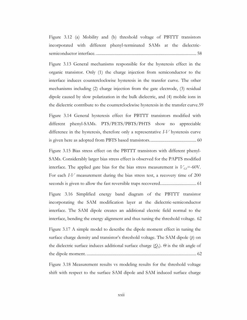
Figure 3.12 (a) Mobility and (b) threshold voltage of PBTTT transistors
incorporated with different phenyl-terminated SAMs at the dielectric-
semiconductor interface. .............................................................................................. 58
Figure 3.13 General mechanisms responsible for the hysteresis effect in the
organic transistor. Only (1) the charge injection from semiconductor to the
interface induces counterclockwise hysteresis in the transfer curve. The other
mechanisms including (2) charge injection from the gate electrode, (3) residual
dipole caused by slow polarization in the bulk dielectric, and (4) mobile ions in
the dielectric contribute to the counterclockwise hysteresis in the transfer curve.59
Figure 3.14 General hysteresis effect for PBTTT transistors modified with
different phenyl-SAMs. PTS/PETS/PBTS/PHTS show no appreciable
difference in the hysteresis, therefore only a representative I-V hysteresis curve
is given here as adopted from PBTS based transistors............................................ 60
Figure 3.15 Bias stress effect on the PBTTT transistors with different phenyl-
SAMs. Considerably larger bias stress effect is observed for the PAPTS modified
interface. The applied gate bias for the bias stress measurement is VGS=-60V.
For each I-V measurement during the bias stress test, a recovery time of 200
seconds is given to allow the fast reversible traps recovered.................................. 61
Figure 3.16 Simplified energy band diagram of the PBTTT transistor
incorporating the SAM modification layer at the dielectric-semiconductor
interface. The SAM dipole creates an additional electric field normal to the
interface, bending the energy alignment and thus tuning the threshold voltage. 62
Figure 3.17 A simple model to describe the dipole moment effect in tuning the
surface charge density and transistor’s threshold voltage. The SAM dipole (p) on
the dielectric surface induces additional surface charge (QS). Θ is the tilt angle of
the dipole moment. ....................................................................................................... 62
Figure 3.18 Measurement results vs modeling results for the threshold voltage
shift with respect to the surface SAM dipole and SAM induced surface charge
xxiii
density. Both p-type PBTTT transistors and n-type PCBM transistors are
measured in this work. ..................................................................................................65
Figure 3.19 Schematic illustration of the proposed electric shielding tensors
effect of the SAM at the dielectric-semiconductor interface: strong external
interfacial electric field as induced by the gate voltage would distort the inherent
dipole moment of the SAM molecule, thus influencing the performance and
reliability of the organic transistors. ............................................................................66
Figure 4.1 A generalized 1-D representation of the physical process dominating
the device operation for organic transistors...............................................................70
Figure 4.2 The energy level diagram of the metal-organic semiconductor
interface. ..........................................................................................................................73
Figure 4.3 The calculated boundary condition for diffusion-limited charge
injection at metal-organic semiconductor interface. .................................................75
Figure 4.4 (a) Schematic illustration of the transition region close to the contact
and the channel region in the organic semiconductor film; (b) The DOS profiles
of the transition region and the major channel based on the mobility edge
model; (c) An equivalent representation of (b) with the critical energy for both
regions set to be identical to simplify the mathematical derivation........................77
Figure 4.5 The relationship between the tail width of localized states (∆Etail), the
relative Fermi energy level (Ef-E0), and the applied gate voltage (VGS). The
following conditions are employed for the calculation here: 300 nm SiO2 gate
dielectric, Von=0 V, h=1 nm, Ntail=1021/cm3, Ec=40 meV, T=300 K. ...................81
Figure 4.6 Simulation results of the (a) output and (b) transfer characteristics,
based on the universal device model introduced in Section 4.2. In addition to
parameters given in Table 4.1, the followings are included: L=10 µm, γ(tr)(1/Tn)=
0.001 cm1/2V-1/2, γ(ch)(1/Tn)=0, (a) φb=0.7 or 0.2 eV, σ=0.1 eV, and (b) φb=0.7 eV,
xxiv
σ=0.1 eV. Note: for the transfer curve simulation, an Ioff (IDS@VGS=0)=1 pA is
assumed per practical situations. ................................................................................. 91
Figure 4.7 (a) Our simulated surface potential profile of a representative organic
transistor operating in different conditions, either in linear regime or saturation
regime, upon the applied drain voltage, VDS, for a fixed gate voltage of VGS=-
100 V. Here T=300 K. (b) A representative surface potential profile of the
P3HT polymer transistor, as recorded in experiments by noncontact
potentiometry using scanning Kelvin probe microscope by Bürgi et al. [112].,
copyright © American Institute of Physics (AIP) 2003........................................... 93
Figure 4.8 Simulated surface potential profiles along the channel direction for
the same transistor only with different injection barrier height (φb=0.7 eV or 0.3
eV) and localized trap states tail width (σ=100 meV or 50 meV). The inset is a
magnified view in the 200 nm region close to the source contact. ........................ 94
Figure 4.9 Mobility scaling behavior with respect to different physical origins
including carrier injection barrier height (φb), localized trap states energy
distribution (σ), Poole-Frenkel like field dependence of carrier mobility (γ(1/Tn)),
and channel length dependent film crystallinity (γc). For simplicity of the
simulation here, the film crystallinity effect is lumped into the mobility’s electric
field effect. ...................................................................................................................... 98
Figure 4.10 Measurement results of the extrinsic field-effect mobility with
respect to different channels for the solution-shearing processed polycrystalline
4T-TMS SPOFETs. The device fabrication and measurement are detailed in
Chapter 2. All of these devices are fabricated on the same wafer with the same
process. The dashed line is for visual guidance and refers to the modeling and
simulation results shown in Figure 4.9. It is found that the finding based on our
model is in excellent agreement with the experimental results............................... 99
xxv
Figure 5.1 Device structure and process flow of the Au/Si3N4/pentacene diodes.
Pentacene was chosen for this study since the pinning factor (S=dφb/dψmetal)
S~0.4 is relatively small for the metal/pentacene interface...................................103
Figure 5.2 AFM images of 200 nm pentacene films deposited on Au at room
temperature (a) before and (b) after Si3N4 sputtering deposition. Height scale:
300 nm...........................................................................................................................104
Figure 5.3 I-V measurement results showing the diodes with/without Si3N4
based on evaporated Au pads are regularly shorted due to metal atoms
penetration along the grain boundaries or the roughness-induced vacancies.....104
Figure 5.4 I-V characteristics of the Au/Si3N4/pentacene diodes with different
Si3N4 thicknesses (with Au wire as the top cathode electrode), providing direct
evidence that the Au/pentacene diode has been successfully tuned to rectifying,
quasi-Ohmic, and symmetric tunneling behavior by modulating the Si3N4
thickness. (The effective contact area between Au wire and Si3N4/pentacene is
only a fraction of the wire cross section due to the surface roughness of
Si3N4/pentacene layer, and may vary from device to device. One should note
that the I-V shape giving the diode property is the essence here.).......................106
Figure 5.5 Normalized dynamic resistance (RAC=∂V/∂I) and static resistance
(RDC=V/I) of the Au/Si3N4/pentacene diodes with respect to the Si3N4
thickness, as calculated from their respective I-V measurement curves.
Normalization is based on the fact that the maximum forward-biased diode
current (here at V=+1 V) is less affected by the Si3N4 thickness. Note: The
device with a thick Si3N4 layer (t=6.1 nm) was not normalized here as tunneling
dominates therein.........................................................................................................107
Figure 5.6 Device structure, microscopy image, and process flow of the
Ag/Si3N4/PTCDA diodes. PTCDA was chosen here since the pinning factor
(S=dφb/dψmetal) is S~0 for metal/PTCDA interface, indicating very strong Fermi-
level pinning effect at the metal/PTCDA interface................................................108
xxvi
Figure 5.7 (a) A quick and straightforward extraction method for the relative
contact resistance of the diodes with different Si3N4 thicknesses, through
measurement of the I-V characteristics on two adjacent electrodes; (b) A
minimum contact resistance is observed at the Ag/PTCDA interface with a
sandwiched Si3N4 thickness of ~2.5 nm, reaffirming the Fermi-level depinning at
M/O interfaces by inserting the ultrathin interfacial Si3N4 layer.......................... 109
Figure 5.8 Different mechanisms of Fermi-level pinning at the metal/organic
semiconductor interface, including (a) MIGS and intrinsic surface states, (b)
charge transfer, (c) covalent bonding, (d) permanent molecular dipole, (e) image
force, and (f) exchange/Pauli repulsion. An interface dipole is always created
upon the M/O junction formation........................................................................... 110
Figure 5.9 M/O interface energy band diagrams based on the proposed lumped
interface dipole model: (a) before M/O interface formation; (b) upon M/O
interface formation, Fermi-level pinning arises from various interface dipole
elements; (c) after inserting an ultrathin Si3N4 insulator, the Fermi-level
depinning takes effect by blocking the physisorption/chemisorption................ 112
Figure 5.10 Simulation results based on the proposed simple depinning model
showing the dominant mechanisms responsible for the contact resistance
behavior after insertion of the ultrathin insulating layer at the M/O interface. 114
1
Chapter 1
Introduction
We choose to go to the moon. We choose to go to the moon in this decade and do the other
things, not because they are easy, but because they are hard, because that goal will serve to
organize and measure the best of our energies and skills, because that challenge is one that we
are willing to accept, one we are unwilling to postpone, and one which we intend to win.
- John F. Kennedy, 1962
Imagine a world filled with flexible personal digital assistants (PDA) or cellphones,
large-area rollable displays, bendable scanners, wearable electronic clothes, as well as
many other electronic devices with versatile functions, fantastic appearance and
mechanical flexibility. An intuitive question would be if there is any possibility to
integrate the well-established semiconductor device technology traditionally based on
silicon hard materials into these novel applications. The prospect seems optimistic, yet,
significant challenges remain both in scientific understanding of the newly emerging
phenomena and in engineering of the reliable devices.
2 CHAPTER 1. INTRODUCTION
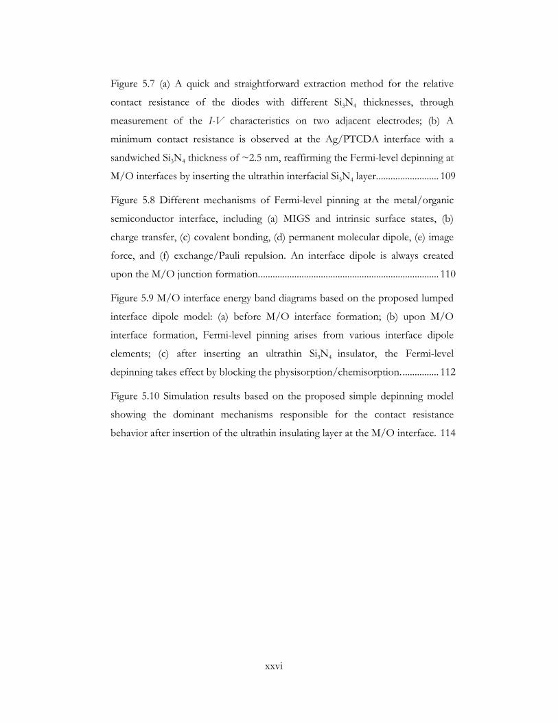
1.1 Historical Overview of Semiconductor Electronics
It is natural to learn from history since history always guides future. Along with the
development of semiconductor electronics over the past few decades, people have been
broadly exploring two intriguing fields: How to make the devices extremely small?
And, how to make the systems extremely large?
Specifically, the first one is toward the limit of scaling down each component,
namely for “nanoelectronics” nowadays, and the other one is toward the limit of scaling
up the system, namely for “macroelectronics”. Identifying their specific applications and
understanding their unique characteristics are required for the success in engineering
devices and systems toward both extremes. To be accurate while without loss of
generality, we’ll focus on discussing a most representative and impotant applications for
each area, i.e. very large scale integration (VLSI) circuit chips and large area displays,
respectively. Figure 1.1 shows the historical development of traditional silicon metal-
oxide-semiconductor field-effect transistors (MOSFET) which is the central component
of VLSI chips. The primary focuses in such nanoelectronics area include reducing the
cost per function or cost per transistor, scaling down of the device to smaller feature
size, packing higher integration density, increasing circuit operation speed, and
minimizing chip power dissipation. The future, however, is challenged by the scaling
bottleneck beyond current 15/22 nm feature size due to fundamental physical effects
arising from materials, processes, and the device architectures [1].
In contrast, for macroelectronic applications as represented by displays, efforts are
centered on reducing the cost per area in addition to expanding the system to larger size
with increased resolution, higher mechanical flexibility, enhanced robustness, and lighter
weight. The requirements of the dimensional scale and operation frequency on its core
component for the backplane, typically hydrogenated amorphous silicon (α-H:Si) or
polycrystalline silicon thin-film transistors (TFT), are less stringent than the MOSFETs
used for high-performance VLSI circuits. The future of macroelectronic applications
relies more heavily on the cost per area and ubiquity limit opposed by traditional
materials, processes, and devices employed in the large-area electronics.
CHAPTER 1. INTRODUCTION 3
1970 1980 1990 2000 2010 202010-9
10-7
10-5
10-3
10-1
101
Year
Cos
t per
Tra
nsis
tor (
$)
100
101
102
103
104 Minim
um Feature S
ize (nm)
Figure 1.1 The historical development of traditional silicon metal-oxide-semiconductor field-effect transistors (MOSFET) used for VLSI circuits. Source data: Intel and ITRS.1
1.2 Carbon Materials for Nano- and Macro-Electronics
In order to circumvent the aforementioned limits, there has been extensive research
work in recent years on exploring novel semiconductor materials and their relevant
processes and devices. Among many others, carbon (organic) electronic materials are
found very promising in both nanoelectronics and macroelectronics areas. Carbon
electronics has emerged as a fast-growing field covering a broad range from
nanoelectronic devices to macroelectronic systems.
On one hand, individual carbon nanotube, graphene, organic molecule, or carbon
nanoribbon was reported having superior electrical properties with extraordinary
intrinsic carrier mobility over 100,000 cm2/Vs, up to 1,000 times higher than in bulk
silicon [2-3]. Consequently, single-graphene [4] or single-carbon nanotube transistor [5]
provides a possible route toward extending the scaling limit of traditional silicon
1 Intel and Dataquest reports (December 2002), see Gordon E. Moore, “Our Revolution”, http://www.sia-online.org/galleries/default-file/Moore.pdf; International Technology Roadmap for Semiconductors (ITRS), http://www.itrs.net/
4 CHAPTER 1. INTRODUCTION
MOSFET. The main hurdle at present is the poor reproducibility of identical devices
required for large scale integrated circuits. How to precisely control the device
placement and integration at will is a major challenge on pushing forward the carbon
nanomaterials into high performance nanoelectronic applications.
On the other hand, carbon nanotube, small-molecule and polymer organic
semiconductor thin-film1 transistors can be readily fabricated with large-scale control of
positioning and integration, though the electrical performance and dimensional scaling
capability is more confined. Typically, the carrier mobility in these thin films is on the
order of 0.1-10 cm2/Vs [6], two to three orders lower than that in single crystal silicon,
thus being inappropriate for high speed computing where traditional single crystal
silicon still dominates. Fortunately, such performance still approaches, if not surpasses,
that of hydrogenated amorphous silicon (α-Si:H) TFTs which are widely used in display
backplanes [7]. Moreover, their unique possibility of low-temperature deposition and
excellent mechanical flexibility enable us to fabricate large-area electronics on flexible,
light-weight substrates using low-cost unconventional means, such as room-temperature
printing and roll-to-roll processing [8]. Therefore, carbon semiconductor based thin film
devices are highly promising for novel and practical macroelectronic applications where
relatively low mobility 2 and medium device feature size satisfy the requirements.
Foreseeable examples include electronic paper, flexible displays, ubiquitous electronic
walls, organic radio-frequency identification (RFID) tags, organic solar cell and light-
emitting diode arrays, chemical sensors, and e-clothes.
For this dissertation work, we focus on studying the organic semiconductor based
thin-film transistors for the aforementioned macroelectronics and flexible electronics
applications.
1 Thin film typically consists of arrays or a number of individual molecules or nanotubes that form a thin layer of film. 2 In comparison to single crystal silicon or individual carbon nanotube, graphene, and nanoribbon for high performance nanoelectronic devices.
CHAPTER 1. INTRODUCTION 5
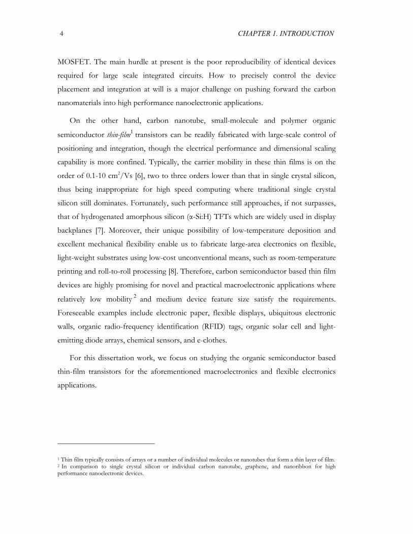
1.3 Motivations and Objectives
As discussed in Section 1.2, organic semiconductor based thin-film transistors have
attracted wide attention in recent years due to their promise in low-cost, large-area,
flexible electronics and the compatibility with scalable fabrication process. Figure 1.2
illustrates the typical structure of a bottom gate, top contact and bottom gate, bottom
contact organic TFT. Besides conducting materials for the source (S), drain (D), and
gate (G), dielectrics for isolating the channel from the gate and organic semiconductor
thin films acting as the active channel are also crucial to the organic TFT operation.
GDielectric
Organic Semiconductor Thin FilmS D
GDielectric
S Organic Semiconductor D
Figure 1.2 Schematic structure of a typical (a) bottom-gate, top-contact and (b)bottom-gate, bottom-contact organic TFT. S: source, D: drain, G: gate.
Of particular interest in the device fabrication is how to deposit the active channel
materials. In general, organic semiconductor thin films can be either vapor processed or
solution processed, depending on their physical and chemical properties. Vacuum
evaporation as a mature fabrication technology is widely used for most organic small-
molecule semiconductors to grow highly uniform films on the substrate. This is
particularly important for large area circuits and systems. However, vapor process
suffers from relatively high temperature in evaporation, high fabrication cost from
expensive setup and material waste, and low throughput as confined by the equipment
space.
An alternative to the vacuum evaporation deposition method is solution processing.
The concept is simple: when the materials are soluble to some specific solvents, one can
6 CHAPTER 1. INTRODUCTION
deposit the film by drop casting, spin-coating, or other ways from the material’s solution
phase [9]. Advantages of solution processing of organic semiconductors include:
(1) It is compatible with printing techniques toward printed electronics1. Since
the devices can be fabricated with screen printing [10], inkjet printing [11-13],
or microcontact printing [14], they possess benefits from all these well-
developed existing processes.
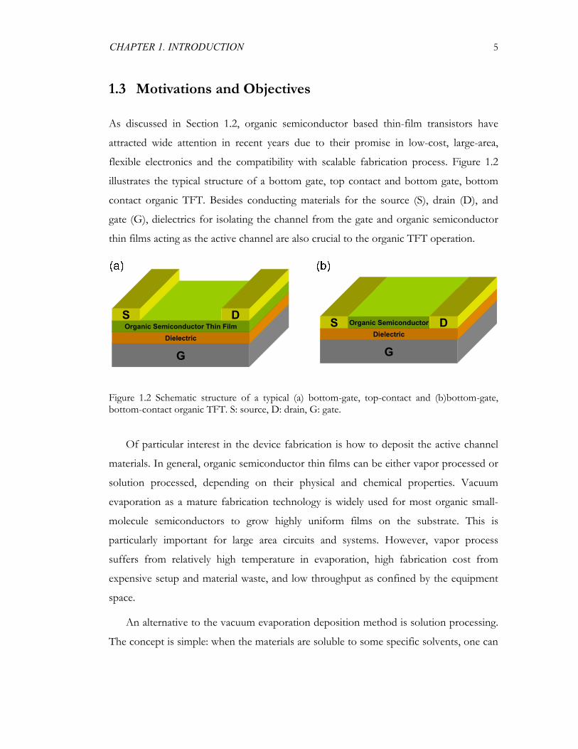
(2) It is possible to manufacture the devices on flexible substrates using a fast,
roll-to-roll process. Figure 1.3 shows a conceptual roll-to-roll manufacturing
process for solution processed organic transistors. The flexible substrate
moves between two end rollers; modules (1)-(n) serve different layer
depositions. Configurations for each module include three substrate-
supporting transfer rollers, a shearing roller clamping the substrate with
designed pressure, and an organic solution tank close to the shearing roller.
Figure 1.3 A proposed roll-to-roll manufacturing process for solution processed organic thin-film transistors.
1 See http://flextech.org/.
CHAPTER 1. INTRODUCTION 7
(3) Low temperature processing becomes available. In solution phase deposition,
the temperature is typically below 100ºC or even down to room temperature,
being significantly lower than that required in vapor process [15].
(4) There is no throughput limit against evaporation setup space.
(5) Self-assembly in solution phase provides a novel method for versatile
patterning of the devices [16-17].
(6) The fabrication cost is considerably reduced based on the above superiority.
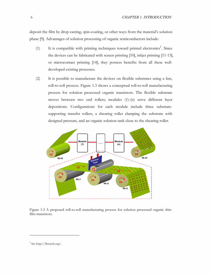
Despite the great potential of solution processed organic thin-film field-effect
transistors (SPOFET), their electrical performance as show in Figure 1.4 is still lagging
behind the counterparts based on vapor process due to unfavorable film microstructures
and poor uniformity. A number of issues remain for SPOFET although the
performance has been improved dramatically in the past decade.
Figure 1.4 A historical overview of the organic transistor performance based on different materials and processes. Adapted from [18]. Copyright © 2005 IEEE.
8 CHAPTER 1. INTRODUCTION
First, it is challenging to fabricate uniform and highly crystalline films via solution
deposition of small-molecule organic semiconductors, albeit many novel techniques
have been proposed [9]. Polymer semiconductors can be readily spin coated from
solution phase to yield uniform films, but the mobility in general is inferior to that of
small molecules as shown in Figure 1.4. Finding an efficient and optimized solution
process is thus important, especially for small-molecule organic semiconductor based
transistors.
Secondly, SPOFETs fabricated on flexible substrates normally show lower
performance as compared to their counterparts on rigid substrates such as on silicon or
glass. It is essential to achieve high performance SPOFETs on flexible substrates,
including both high mobility and steep subthreshold slope, toward practical flexible
electronics applications.
Additionally, the device physics of organic thin-film field-effect transistors,
especially SPOFETs, remains elusive in many aspects [19]. For instance, further
fundamental understanding and studies are in demand for charge transport properties in
the organic semiconductor films, change injection or contact properties at the metal-
organic semiconductor interface, and interface properties between the organic
semiconductor and the dielectric, all of which are critical in determining the device
performance and device engineering protocols.
Lastly, unlike that for traditional silicon MOSFET where industrial standard device
modeling and simulation programs have been well established1, modeling and simulation
for organic transistors remain as a challenging task. Indeed, a device model
incorporating the fundamental physical effects must also help resolve many elusive
phenomena observed from the electrical characterization.
In this dissertation, we address all the above issues and focus on the study of device
physics, device modeling, fabrication technology, and interface engineering for solution-
processed organic field-effect transistors for flexible electronics applications.
1 For instance, TCAD Sentaurus from Synopsys Inc., http://www.synopsys.com/tools/tcad
CHAPTER 1. INTRODUCTION 9
1.4 Organization of this Dissertation
The remainder of this dissertation is organized as follows.
Chapter 2 presents the design and demonstration of high-performance, low-voltage
flexible SPOFETs fabricated on plastic substrates with a carrier mobility over 0.2
cm2/Vs, a turn-on voltage of near 0 V, and a record low subthreshold slope of ~80
mV/dec in ambient conditions. These exceptional characteristics are achieved by novel
device architecture design, 3-D statistical modeling for solution-shearing process
optimization, and phenyl-terminated self-assembled monolayer (SAM) based interface
engineering.
In Chapter 3, we systematically investigate dipole moment related physical effects
and chemistry effects of the SAM at the organic semiconductor-dielectric interface.
Through careful selection of a group of phenyl-terminated SAMs, we elucidate how the
performance and reliability of organic transistors are controlled by their interface
conditions. In addition, we briefly introduce a simple spin-coating process for depositing
high-quality phenyl-terminated SAMs for organic electronics applications.
Chapter 4 focuses on the device physics and device modeling of organic transistors.
We have developed a universal physical model for organic transistors by incorporating
both charge injection effects at the metal-organic interface and charge transport
properties in the organic semiconductor film, and successfully applied the device model
to resolve many elusive physical phenomena observed so far, such as the peculiar
mobility scaling behavior, the contact resistance effect, and the mysterious surface
potential profiles along the channel which have been experimentally probed yet poorly
understood. The complete model as derived in an analytical manner and the comparison
between simulation results and experimental results are given in detail. Of particular
importance is that we discover an overshoot region in the mobility scaling behavior and
identified the existence of a critical channel length for the peak field-effect mobility.
To the end of lowering charge injection barrier and reducing the interfacial disorder
width or localization states, in Chapter 5, we explore and demonstrate Fermi-level
10 CHAPTER 1. INTRODUCTION
depinning at the metal-organic interface for low-resistance Ohmic contacts by inserting
an ultrathin interfacial Si3N4 insulator in between. The contact behavior is successfully
tuned from rectifying to quasi-Ohmic and to tunneling by varying the Si3N4 thickness
within 0-6 nm. Detailed physical mechanisms of Fermi-level pinning/depinning
responsible for the metal-organic semiconductor contact behavior are clarified based on
a proposed lumped-dipole model.
We discuss the future work and conclude this dissertation in Chapter 6.
11
Chapter 2
High-Performance Solution
Processed Flexible Organic
Transistor
Logic will get you from A to B. Imagination will take you everywhere.
- Albert Einstein
As outlined in the previous chapter, there are increasing research efforts focusing on
solution-processed organic field-effect transistors (SPOFET) due to their promise in
large-area electronics fabricated on flexible substrates using low-cost unconventional
means, such as low/room-temperature printing and roll-to-roll processing [6, 9].
Pioneering works on flexible, solution-processed organic transistors in the past decade have
demonstrated many intriguing applications on plastic substrates, including all-polymer
integrated circuits [12, 20], flexible smart pixels [12, 21], plastic sensors [22], rollable
1 Note: Portions of this chapter are reproduced, with permission, from [15] © 2009 IEEE, [36] © 2009 American Institute of Physics and [37] © 2008 IEEE.
12 CHAPTER 2. SOLUTION-PROCESSED FLEXIBLE ORGANIC TRANSISTOR
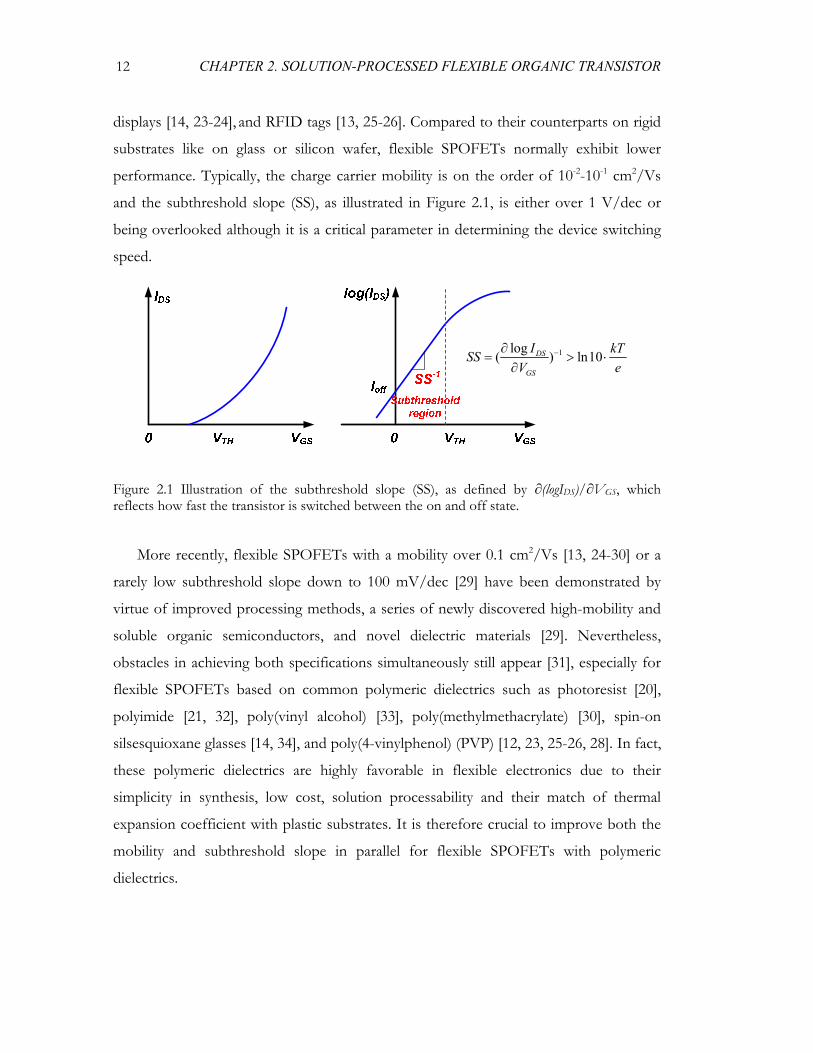
displays [14, 23-24], and RFID tags [13, 25-26]. Compared to their counterparts on rigid
substrates like on glass or silicon wafer, flexible SPOFETs normally exhibit lower
performance. Typically, the charge carrier mobility is on the order of 10-2-10-1 cm2/Vs
and the subthreshold slope (SS), as illustrated in Figure 2.1, is either over 1 V/dec or
being overlooked although it is a critical parameter in determining the device switching
speed.
1log( ) ln10DS
GS
I kTSSV e
−∂= > ⋅
∂
Figure 2.1 Illustration of the subthreshold slope (SS), as defined by ∂(logIDS)/∂VGS, which reflects how fast the transistor is switched between the on and off state.
More recently, flexible SPOFETs with a mobility over 0.1 cm2/Vs [13, 24-30] or a
rarely low subthreshold slope down to 100 mV/dec [29] have been demonstrated by
virtue of improved processing methods, a series of newly discovered high-mobility and
soluble organic semiconductors, and novel dielectric materials [29]. Nevertheless,
obstacles in achieving both specifications simultaneously still appear [31], especially for
flexible SPOFETs based on common polymeric dielectrics such as photoresist [20],
polyimide [21, 32], poly(vinyl alcohol) [33], poly(methylmethacrylate) [30], spin-on
silsesquioxane glasses [14, 34], and poly(4-vinylphenol) (PVP) [12, 23, 25-26, 28]. In fact,
these polymeric dielectrics are highly favorable in flexible electronics due to their
simplicity in synthesis, low cost, solution processability and their match of thermal
expansion coefficient with plastic substrates. It is therefore crucial to improve both the
mobility and subthreshold slope in parallel for flexible SPOFETs with polymeric
dielectrics.
CHAPTER 2. SOLUTION-PROCESSED FLEXIBLE ORGANIC TRANSISTOR 13
In this chapter, we address the above issue through a combination of the device
architecture design, solution process optimization, organic semiconductor/polymeric
dielectric development [35] and their interface engineering. Flexible SPOFETs
fabricated and tested in ambient conditions on rough plastic with a high mobility over
0.2 cm2/Vs, a turn-on voltage of near 0 V, and a subthreshold slope of ~80 mV/dec
have been successfully demonstrated [36].
2.1 Flexible SPOFET Device: Design and Fabrication
We emphasize that both the mobility and the subthreshold slope of organic transistors
rely on the semiconductor film crystallinity and the interface conditions. Therefore,
priorities for the design and fabrication of our flexible SPOFET devices are minimizing
interface and bulk trap states and enhancing the organic film crystallinity.
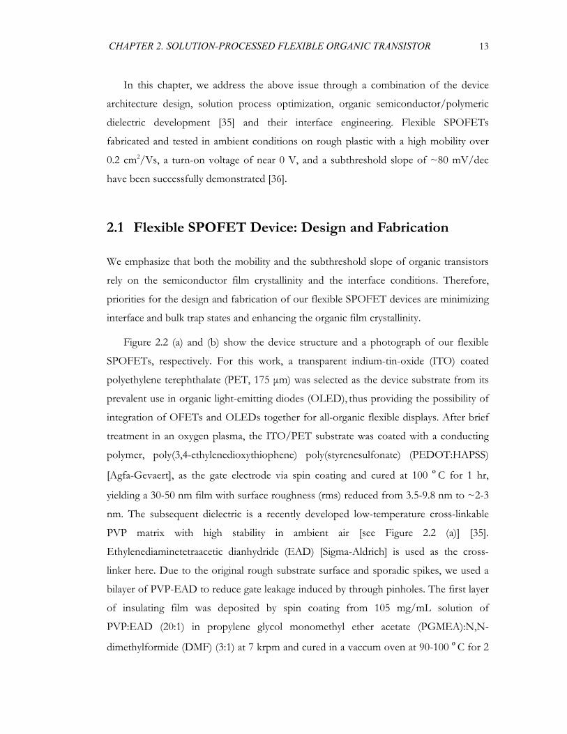
Figure 2.2 (a) and (b) show the device structure and a photograph of our flexible
SPOFETs, respectively. For this work, a transparent indium-tin-oxide (ITO) coated
polyethylene terephthalate (PET, 175 μm) was selected as the device substrate from its
prevalent use in organic light-emitting diodes (OLED), thus providing the possibility of
integration of OFETs and OLEDs together for all-organic flexible displays. After brief
treatment in an oxygen plasma, the ITO/PET substrate was coated with a conducting
polymer, poly(3,4-ethylenedioxythiophene) poly(styrenesulfonate) (PEDOT:HAPSS)
[Agfa-Gevaert], as the gate electrode via spin coating and cured at 100 ºC for 1 hr,
yielding a 30-50 nm film with surface roughness (rms) reduced from 3.5-9.8 nm to ~2-3
nm. The subsequent dielectric is a recently developed low-temperature cross-linkable
PVP matrix with high stability in ambient air [see Figure 2.2 (a)] [35].
Ethylenediaminetetraacetic dianhydride (EAD) [Sigma-Aldrich] is used as the cross-
linker here. Due to the original rough substrate surface and sporadic spikes, we used a
bilayer of PVP-EAD to reduce gate leakage induced by through pinholes. The first layer
of insulating film was deposited by spin coating from 105 mg/mL solution of
PVP:EAD (20:1) in propylene glycol monomethyl ether acetate (PGMEA):N,N-
dimethylformide (DMF) (3:1) at 7 krpm and cured in a vaccum oven at 90-100 ºC for 2
14 CHAPTER 2. SOLUTION-PROCESSED FLEXIBLE ORGANIC TRANSISTOR
hr to promote the cross-linking reaction. The second layer was spin-coated from a lower
concentration of PVP:EAD solution of 63 mg/mL at 5 krpm to better tune the surface
morphology and eliminate pinholes in the dielectric, and again followed by annealing.
Bilayer PVP-EADPEDOT:PSSITO
500 nm
ITO
PET(Polyethylene-Terephthalate)
Bilayer Cross-linked PVP (PVP-EAD)
Au
PEDOT:PSS
Au
SS S
S Si
175 μm
4T-TMSPBTS-SAM
N
O
O
n
OHO
N
O
O
n
OOH
SiO O
O
SiO
O
SiO
O
SiO
O
(a)
(b) (c)
Figure 2.2 (a) Device structure and (b) photograph of our flexible 4T-TMS SPOFETs. (c) Scanning electron microscopy (SEM) image of the bilayer PVP-EAD dielectric that possesses apparent single-layer morphology. SEM was performed at 3 keV in a tilt angle of 45º on an deliberately peeled-off area to examine both the surface and the cross section.
As shown in Figure 2.2 (c), our bilayer PVP-EAD dielectric of ~180 nm possesses
apparent single-layer morphology without distinguishable traces in between or on the
top surface, as revealed by scanning electron microscopy (SEM) [FEI XL30 Sirion]. The
device yield based on this bilayer PVP-EAD was found 50-60% higher than that of
CHAPTER 2. SOLUTION-PROCESSED FLEXIBLE ORGANIC TRANSISTOR 15
single layer dielectric. Typical surface roughness value of the bilayer PVP-EAD dielectric
is ~0.8-1.3 nm (rms).
Since phenyl-terminated self-assembled monolayers (SAM) have been found
advantageous in solution processing of organic transistors due to their decent tradeoff
between wettability and surface energy [15] as detailed in Section 2.1.2 and Chapter 3,
here, we applied 4-phenylbutyltrichlorosilane (PBTS) to modify the PVP-EAD dielectric
surface via spin coating, resulting in a high water contact angle of ~86ºwhile still
maintaining excellent wettability for organic semiconductor solutions. Systematic study
of the phenyl-terminated SAM effects will be presented in Chapter 3.
A subsequent critical step in fabricating these flexible SPOFETs is the deposition of
the organic semiconductor thin films. Here we used a recently synthesized p-type small-
molecule organic semiconductor, trimethyl-[2,2';5',2'';5'',2'''] quarter-thiophen-5-yl-silane
(4T-TMS) [the synthesis details reported by Dr. Mark Roberts in [35]; chemical structure
shown in Figure 2.2 (a)]. 4T-TMS is an air-stable and solution-processable organic
material which shows relatively high carrier mobility. To deposit 4T-TMS thin films as
the transistor’s active layer, we introduce a solution-shearing process that has been
demonstrated with capability of fast screening small-molecule semiconductor
performance [37-39]. The details of the material characterization and the 3-D statistical
process optimization will be given in the following section.
To complete the top-contact flexible 4T-TMS SPOFETs shown in Figure 2.2, 40
nm gold source and drain electrodes were thermally evaporated onto the 4T-TMS films
through a shadow mask at a rate of ~0.5 Å/s. Material Characterization and Process
Optimization
2.1.1 4T-TMS Electronic Properties
Rational design of an electronic device requires understanding of the physical and
electronic properties of its materials as well as the device energy band diagrams. Figure
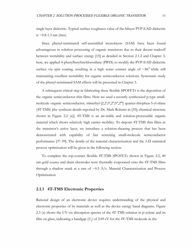
2.3 (a) shows the UV-vis absorption spectra of the 4T-TMS solution in p-xylene and its
film on glass, indicating a bandgap (Eg) of 2.69 eV for the 4T-TMS molecule in the
16 CHAPTER 2. SOLUTION-PROCESSED FLEXIBLE ORGANIC TRANSISTOR
300 400 500 600 700 800
0.00
0.25
0.50
0.75
1.00
Abs
orpt
ion
(a.u
.)
Wavelength (nm)
4T-TMS in solution
4T-TMS in film
-2 -1 0 1
-3
-2
-1
0
1
2
3
Oxidation/Reductionpeak of 4T-TMSmolecule
Cur
rent
(μA
)
Potential (V)
Oxidation/Reduction peak of reference molecule with HOMO=-4.80eV
(a)
(b)
(c)
4.6 4.8 5.0 5.2 5.4 5.6 5.8 6.0 6.2
0
1000
2000
3000
4000
5000
Yie
ld1/
2 (cps
1/2 )
Yield (cps) Yield1/2 (cps1/2)
Energy (eV)
Yie
ld (c
ps)
0
10
20
30
40
50
60
70
Figure 2.3 (a) UV-vis absorption spectra of 4T-TMS in a solution/film phase. (b) Cyclic voltammety (CV) diagram of 4T-TMS with a reference compound of HOMO=-4.80 eV in 1,2-dichlorobenzene. (c) Photoelectron spectroscopy measurement results for 4T-TMS films.
CHAPTER 2. SOLUTION-PROCESSED FLEXIBLE ORGANIC TRANSISTOR 17
solution as estimated from the absorption onset wavelength (λonset=462 nm), and a close
Eg of 2.54 eV for the 4T-TMS film on glass. The highest occupied molecular orbital
(HOMO) energy level of the 4T-TMS molecule was measured using cyclic voltammetry
(CV) [CH Instruments, Inc.] as shown in Figure 2.3 (b) and was estimated from the
onset potential [40] to be around -5.27 eV. The lowest unoccupied molecular orbital
(LUMO) energy level thus can be calculated by ELUMO=EHOMO+Eg=-2.58/-2.73 eV.
Photoelectron spectroscopy (PES) spectra [Model AC-2, Riken Keiki Co.] in Figure 2.3
(c) show the ionization potential of the 4T-TMS thin film is approximately 5.20 eV, in
good agreement with the above electrochemical measurement results.
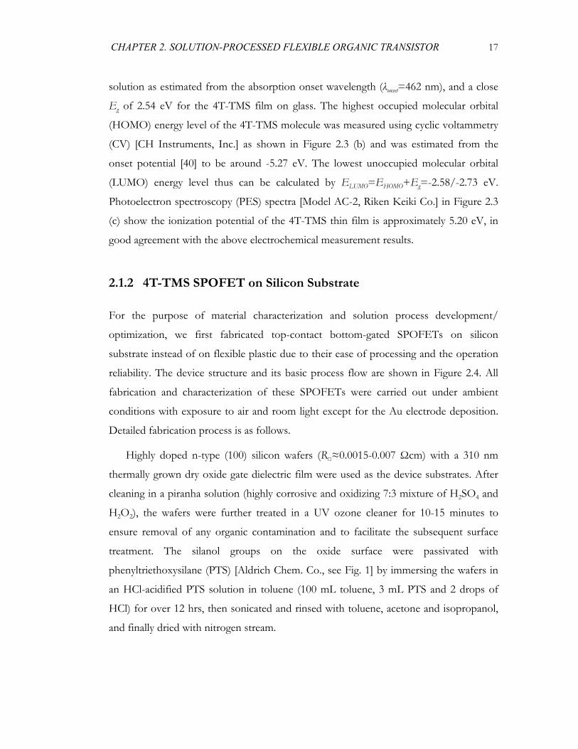
2.1.2 4T-TMS SPOFET on Silicon Substrate
For the purpose of material characterization and solution process development/
optimization, we first fabricated top-contact bottom-gated SPOFETs on silicon
substrate instead of on flexible plastic due to their ease of processing and the operation
reliability. The device structure and its basic process flow are shown in Figure 2.4. All
fabrication and characterization of these SPOFETs were carried out under ambient
conditions with exposure to air and room light except for the Au electrode deposition.
Detailed fabrication process is as follows.
Highly doped n-type (100) silicon wafers (R≈0.0015-0.007 Ωcm) with a 310 nm
thermally grown dry oxide gate dielectric film were used as the device substrates. After
cleaning in a piranha solution (highly corrosive and oxidizing 7:3 mixture of H2SO4 and
H2O2), the wafers were further treated in a UV ozone cleaner for 10-15 minutes to
ensure removal of any organic contamination and to facilitate the subsequent surface
treatment. The silanol groups on the oxide surface were passivated with
phenyltriethoxysilane (PTS) [Aldrich Chem. Co., see Fig. 1] by immersing the wafers in
an HCl-acidified PTS solution in toluene (100 mL toluene, 3 mL PTS and 2 drops of
HCl) for over 12 hrs, then sonicated and rinsed with toluene, acetone and isopropanol,
and finally dried with nitrogen stream.
18 CHAPTER 2. SOLUTION-PROCESSED FLEXIBLE ORGANIC TRANSISTOR
Phenyl-Triethoxy-Silane (PTS)
SiO
O O
SS S
S Si
4T-TMS
Thermally grown SiO2
N++ Si (Gate)
4T-TMS Active LayerD
Phenyl-SAM
S4T-TMS Active Layer
D S
S
S
S
SSi
S
S
S
SSiAu Au
1 Piranha cleaning for the silicon oxide wafer
2 Surface pre-treatment in UV ozone cleaner
3 PTS SAM deposition on the SiO2 surface
5 Solution deposition of 4T-TMS film
6 Annealing in vaccum oven at 80ºC for overnight
7 Thermal evaporation of the Au electrode for S/D
4 Sonication cleaning for the surface, soaked in toluene
Figure 2.4 SPOFET device structure on silicon substrate and its basic fabrication process flow.
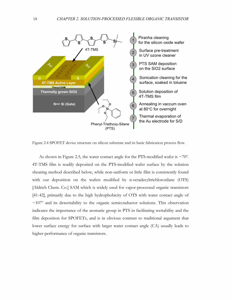
As shown in Figure 2.5, the water contact angle for the PTS-modified wafer is ~70º.
4T-TMS film is readily deposited on the PTS-modified wafer surface by the solution
shearing method described below, while non-uniform or little film is consistently found
with our deposition on the wafers modified by n-octadecyltrichlorosilane (OTS)
[Aldrich Chem. Co.] SAM which is widely used for vapor-processed organic transistors
[41-42], primarily due to the high hydrophobicity of OTS with water contact angle of
~107º and its dewettability to the organic semiconductor solutions. This observation
indicates the importance of the aromatic group in PTS in facilitating wettability and the
film deposition for SPOFETs, and is in obvious contrast to traditional argument that
lower surface energy for surface with larger water contact angle (CA) usually leads to
higher performance of organic transistors.
CHAPTER 2. SOLUTION-PROCESSED FLEXIBLE ORGANIC TRANSISTOR 19
Si
O
O
O
Si
O
O
Si
O
O
Si
O
O
OTS
CA~107O
(a)
(b)
shea
ring
100 µm
Si
O
O
O
Si
O
O
Si
O
O
Si
O
O
PTS
CA~70O
Figure 2.5 Surface structure, water contact angle and cross-polarized microscope image of 4T-TMS film deposited by solution shearing process on (a) PTS treated substrate and (b) OTS treated substrate. Large crystalline domain films can be successfully deposited on PTS substrate, while nonuniform or little film is consistently observed on OTS substrate due to its dewettability to the 4T-TMS organic semiconductor solutions.
4T-TMS solutions are prepared using different solvents, including chlorobenzene, p-
xylene and 1,2-dichlorobenzene, at various concentrations (5 mg/mL-12 mg/mL). Next,
we used spin-coating, drop casting, and solution-shearing [15, 36-39, 43] methods to
deposit 4T-TMS thin films. For the solution-shearing method depicted in Figure 2.6
(experimental setup placed in a fume hood), briefly, a few drops of semiconductor
20 CHAPTER 2. SOLUTION-PROCESSED FLEXIBLE ORGANIC TRANSISTOR
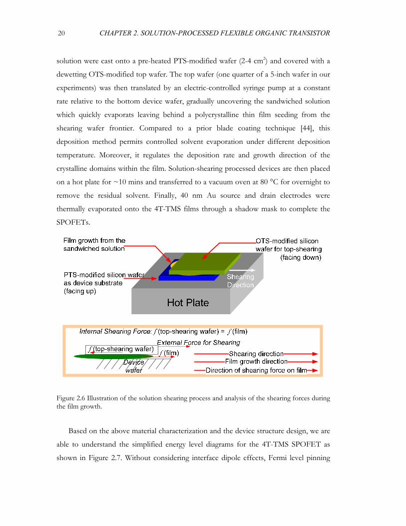
solution were cast onto a pre-heated PTS-modified wafer (2-4 cm2) and covered with a
dewetting OTS-modified top wafer. The top wafer (one quarter of a 5-inch wafer in our
experiments) was then translated by an electric-controlled syringe pump at a constant
rate relative to the bottom device wafer, gradually uncovering the sandwiched solution
which quickly evaporats leaving behind a polycrystalline thin film seeding from the
shearing wafer frontier. Compared to a prior blade coating technique [44], this
deposition method permits controlled solvent evaporation under different deposition
temperature. Moreover, it regulates the deposition rate and growth direction of the
crystalline domains within the film. Solution-shearing processed devices are then placed
on a hot plate for ~10 mins and transferred to a vacuum oven at 80 °C for overnight to
remove the residual solvent. Finally, 40 nm Au source and drain electrodes were
thermally evaporated onto the 4T-TMS films through a shadow mask to complete the
SPOFETs.
Figure 2.6 Illustration of the solution shearing process and analysis of the shearing forces during the film growth.
Based on the above material characterization and the device structure design, we are
able to understand the simplified energy level diagrams for the 4T-TMS SPOFET as
shown in Figure 2.7. Without considering interface dipole effects, Fermi level pinning
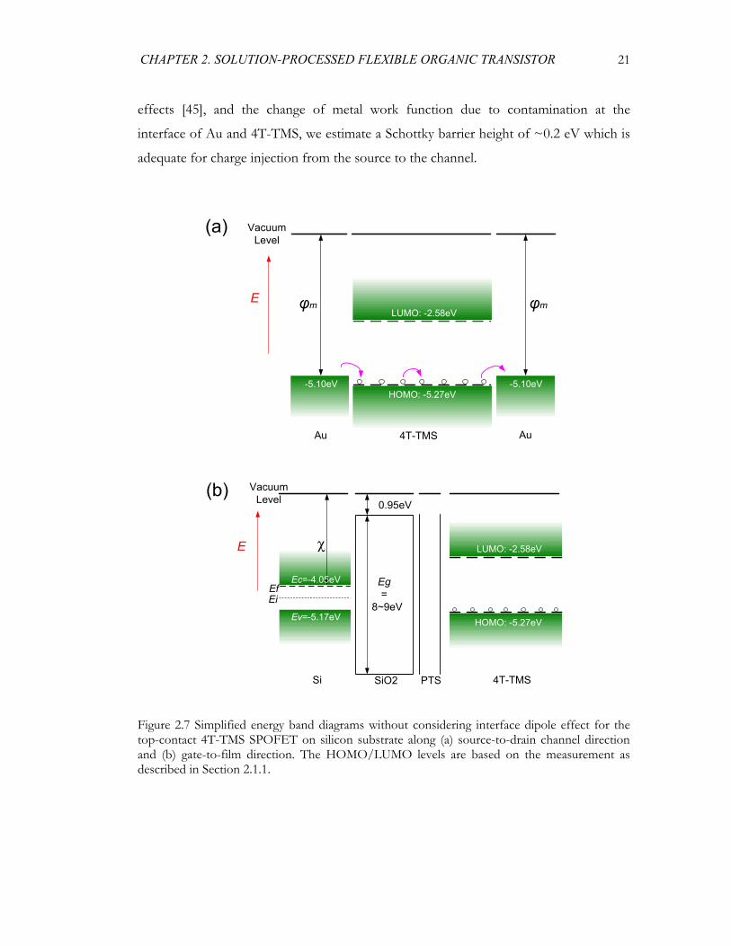
CHAPTER 2. SOLUTION-PROCESSED FLEXIBLE ORGANIC TRANSISTOR 21
effects [45], and the change of metal work function due to contamination at the
interface of Au and 4T-TMS, we estimate a Schottky barrier height of ~0.2 eV which is
adequate for charge injection from the source to the channel.
(a)
(b)
E
-5.10eV
Vacuum Level
φm φm
4T-TMS
-5.10eV
LUMO: -2.58eV
HOMO: -5.27eV
Au Au
E χ
Ev=-5.17eV
EfEi
Ec=-4.05eV Eg=
8~9eV
0.95eV
SiO2
Vacuum Level
4T-TMS
LUMO: -2.58eV
HOMO: -5.27eV
PTSSi
Figure 2.7 Simplified energy band diagrams without considering interface dipole effect for the top-contact 4T-TMS SPOFET on silicon substrate along (a) source-to-drain channel direction and (b) gate-to-film direction. The HOMO/LUMO levels are based on the measurement as described in Section 2.1.1.
22 CHAPTER 2. SOLUTION-PROCESSED FLEXIBLE ORGANIC TRANSISTOR
2.1.3 Comparison of Different Solution Deposition Methods
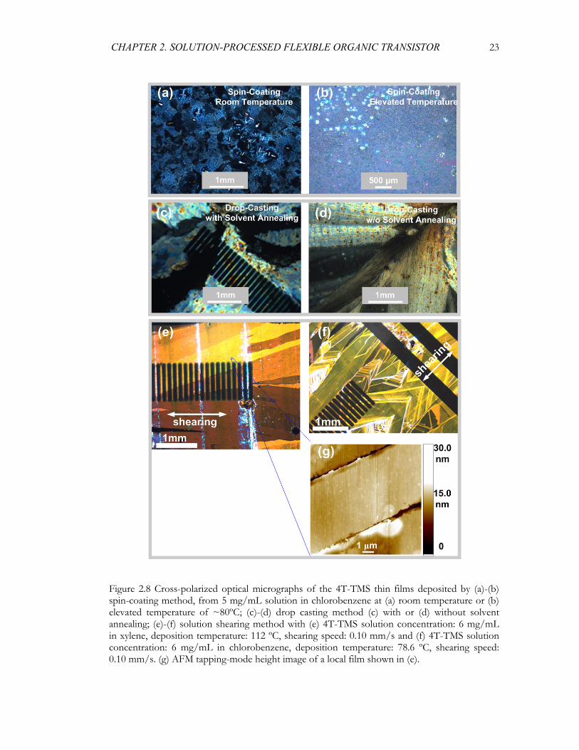
Spin-coating deposition is widely used for polymer semiconductors due to its simplicity
and capability to produce uniform films [8]. However, this method is not ideal for
fabricating high-quality small-molecule semiconductor films due to small molecule’s
lower solution viscosity and higher crystallinity. As a comparison, we fabricated 4T-TMS
SPOFETs by spin-coating from a chlorobenzene solution at both room temperature
and elevated temperature as shown in Figure 2.8 (a) and (b), respectively. These films are
mostly amorphous and rough, giving a low field-effect mobility typically on the order of
10-3 cm2/Vs. Another method to deposit small-molecule semiconductor film from
solution phase is drop-casting, which is essentially the concept used for the ink-jet
printing of organic electronic devices. Drop-casting normally renders undesirable
randomness in crystalline domain orientation within the film as shown in Figure 2.8 (c)-
(d), consequently sacrificing the performance uniformity.
Notably, Figure 2.8 (e)-(f) show the cross-polarized optical micrographs of typical
4T-TMS thin films as deposited by the solution shearing method under optimized
conditions, where the clear birefringence indicates that well-oriented polycrystalline
domains are successfully formed within the sheared films and they tend to have an
elongated shape along the shearing direction. Tapping mode atomic force microscopy
(AFM) image shown in Figure 2.8 (g) over the good film part further corroborates the
well-oriented crystalline domains.
2.1.4 3-D Statistical Process Optimization
Process optimization is critical in achieving high quality films and high performance
devices. Return to the solution shearing process as shown in Figure 2.6, we can find out
at least two apparently competitive mechanisms in determining the crystalline domain
growth, evaporation and crystallization, both ongoing at the shearing wafer frontier.
Moreover, mechanical shearing force might also play a role in the film growth. Without
knowledge of the crystallization and evaporation kinetics parameters for the involved
CHAPTER 2. SOLUTION-PROCESSED FLEXIBLE ORGANIC TRANSISTOR 23
Figure 2.8 Cross-polarized optical micrographs of the 4T-TMS thin films deposited by (a)-(b) spin-coating method, from 5 mg/mL solution in chlorobenzene at (a) room temperature or (b) elevated temperature of ~80ºC; (c)-(d) drop casting method (c) with or (d) without solvent annealing; (e)-(f) solution shearing method with (e) 4T-TMS solution concentration: 6 mg/mL in xylene, deposition temperature: 112 ºC, shearing speed: 0.10 mm/s and (f) 4T-TMS solution concentration: 6 mg/mL in chlorobenzene, deposition temperature: 78.6 ºC, shearing speed: 0.10 mm/s. (g) AFM tapping-mode height image of a local film shown in (e).
24 CHAPTER 2. SOLUTION-PROCESSED FLEXIBLE ORGANIC TRANSISTOR
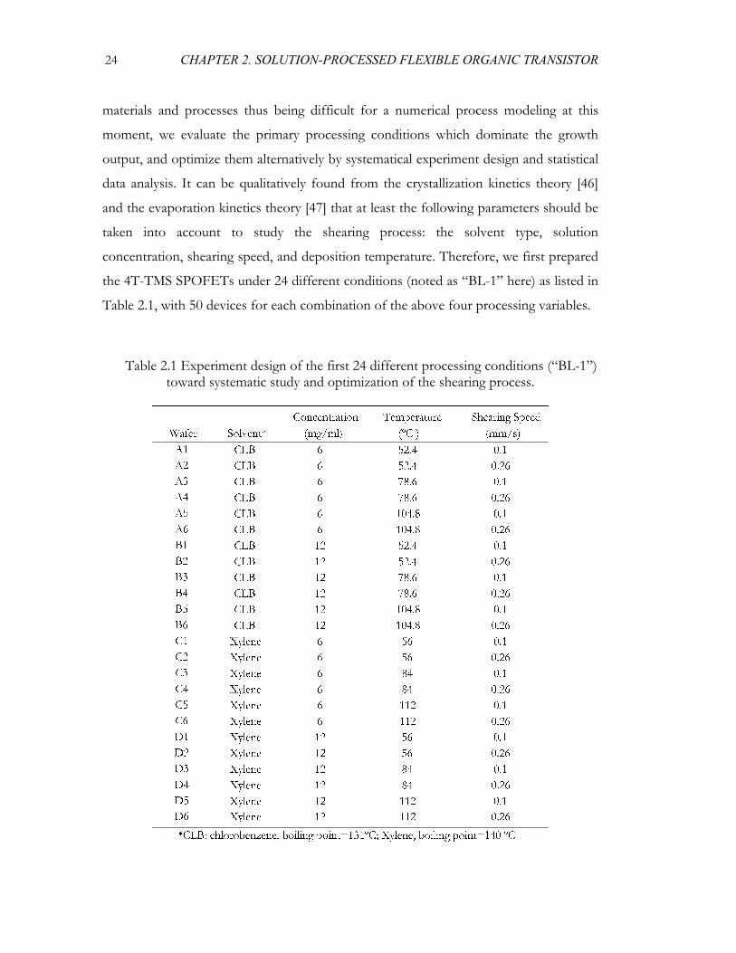
materials and processes thus being difficult for a numerical process modeling at this
moment, we evaluate the primary processing conditions which dominate the growth
output, and optimize them alternatively by systematical experiment design and statistical
data analysis. It can be qualitatively found from the crystallization kinetics theory [46]
and the evaporation kinetics theory [47] that at least the following parameters should be
taken into account to study the shearing process: the solvent type, solution
concentration, shearing speed, and deposition temperature. Therefore, we first prepared
the 4T-TMS SPOFETs under 24 different conditions (noted as “BL-1” here) as listed in
Table 2.1, with 50 devices for each combination of the above four processing variables.
Table 2.1 Experiment design of the first 24 different processing conditions (“BL-1”) toward systematic study and optimization of the shearing process.
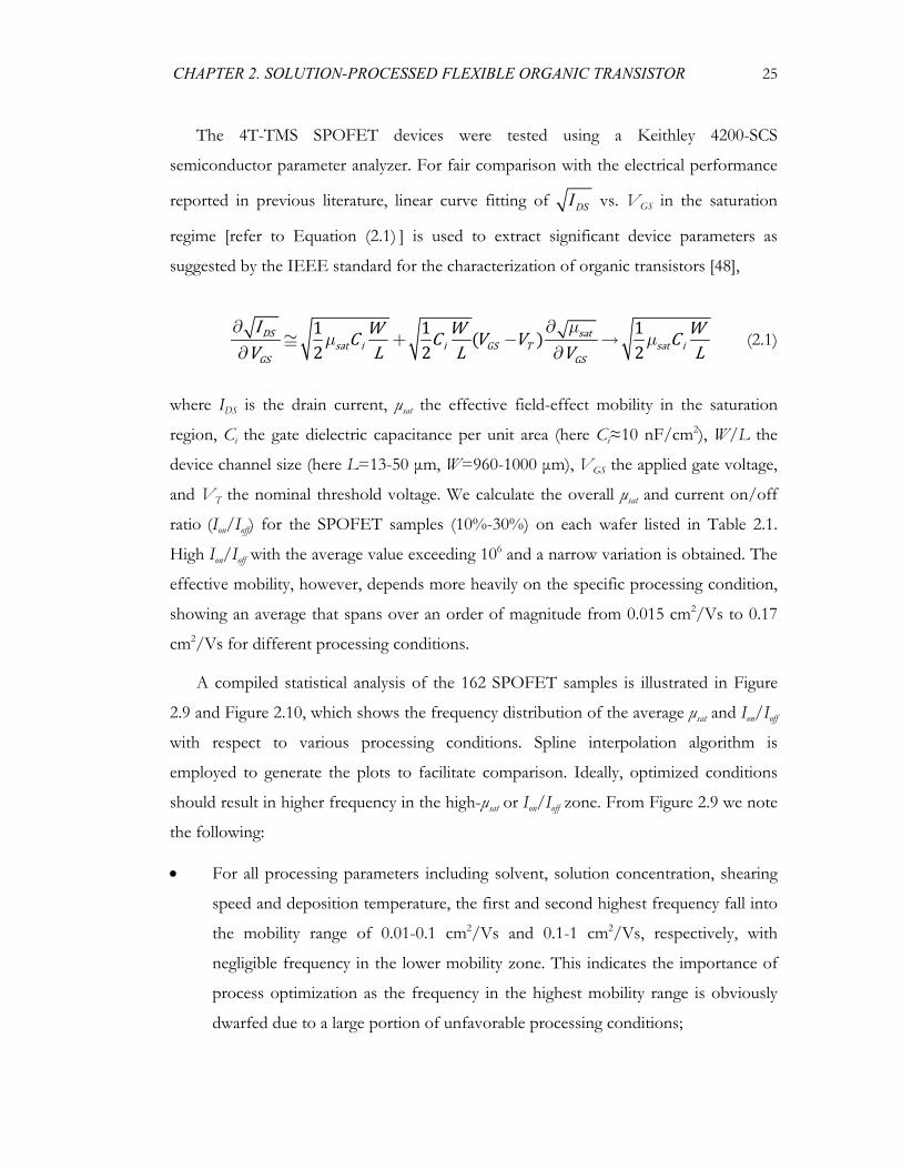
CHAPTER 2. SOLUTION-PROCESSED FLEXIBLE ORGANIC TRANSISTOR 25
The 4T-TMS SPOFET devices were tested using a Keithley 4200-SCS
semiconductor parameter analyzer. For fair comparison with the electrical performance
reported in previous literature, linear curve fitting of DSI vs. VGS in the saturation
regime [refer to Equation (2.1) ] is used to extract significant device parameters as
suggested by the IEEE standard for the characterization of organic transistors [48],
μ
μ μ∂ ∂
≅ + − →∂ ∂
1 1 12 2 2
DS satsat i i GS T sat i
GS GS
I W W WC C V V CV L L V L
(2.1)
where IDS is the drain current, μsat the effective field-effect mobility in the saturation
region, Ci the gate dielectric capacitance per unit area (here Ci≈10 nF/cm2), W/L the
device channel size (here L=13-50 μm, W=960-1000 μm), VGS the applied gate voltage,
and VT the nominal threshold voltage. We calculate the overall μsat and current on/off
ratio (Ion/Ioff) for the SPOFET samples (10%-30%) on each wafer listed in Table 2.1.
High Ion/Ioff with the average value exceeding 106 and a narrow variation is obtained. The
effective mobility, however, depends more heavily on the specific processing condition,
showing an average that spans over an order of magnitude from 0.015 cm2/Vs to 0.17
cm2/Vs for different processing conditions.
A compiled statistical analysis of the 162 SPOFET samples is illustrated in Figure
2.9 and Figure 2.10, which shows the frequency distribution of the average μsat and Ion/Ioff
with respect to various processing conditions. Spline interpolation algorithm is
employed to generate the plots to facilitate comparison. Ideally, optimized conditions
should result in higher frequency in the high-μsat or Ion/Ioff zone. From Figure 2.9 we note
the following:
• For all processing parameters including solvent, solution concentration, shearing
speed and deposition temperature, the first and second highest frequency fall into
the mobility range of 0.01-0.1 cm2/Vs and 0.1-1 cm2/Vs, respectively, with
negligible frequency in the lower mobility zone. This indicates the importance of
process optimization as the frequency in the highest mobility range is obviously
dwarfed due to a large portion of unfavorable processing conditions;
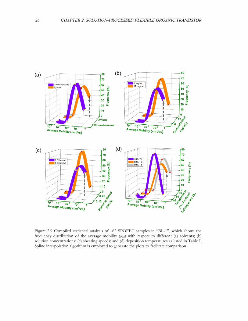
26 CHAPTER 2. SOLUTION-PROCESSED FLEXIBLE ORGANIC TRANSISTOR
Figure 2.9 Compiled statistical analysis of 162 SPOFET samples in “BL-1”, which shows the frequency distribution of the average mobility (μsat) with respect to different (a) solvents; (b) solution concentrations; (c) shearing speeds; and (d) deposition temperatures as listed in Table I. Spline interpolation algorithm is employed to generate the plots to facilitate comparison
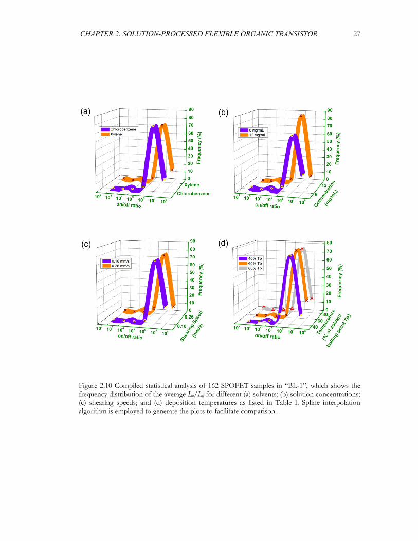
CHAPTER 2. SOLUTION-PROCESSED FLEXIBLE ORGANIC TRANSISTOR 27
Figure 2.10 Compiled statistical analysis of 162 SPOFET samples in “BL-1”, which shows the frequency distribution of the average Ion/Ioff for different (a) solvents; (b) solution concentrations; (c) shearing speeds; and (d) deposition temperatures as listed in Table I. Spline interpolation algorithm is employed to generate the plots to facilitate comparison.
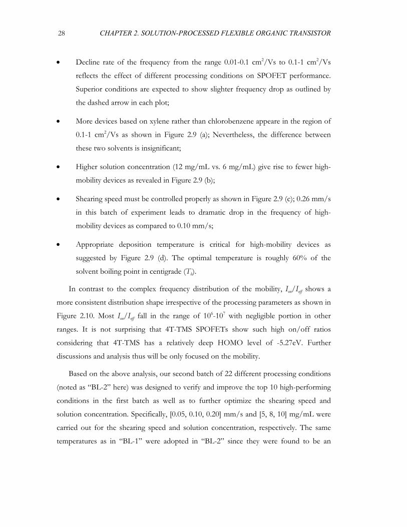
28 CHAPTER 2. SOLUTION-PROCESSED FLEXIBLE ORGANIC TRANSISTOR
• Decline rate of the frequency from the range 0.01-0.1 cm2/Vs to 0.1-1 cm2/Vs
reflects the effect of different processing conditions on SPOFET performance.
Superior conditions are expected to show slighter frequency drop as outlined by
the dashed arrow in each plot;
• More devices based on xylene rather than chlorobenzene appeare in the region of
0.1-1 cm2/Vs as shown in Figure 2.9 (a); Nevertheless, the difference between
these two solvents is insignificant;
• Higher solution concentration (12 mg/mL vs. 6 mg/mL) give rise to fewer high-
mobility devices as revealed in Figure 2.9 (b);
• Shearing speed must be controlled properly as shown in Figure 2.9 (c); 0.26 mm/s
in this batch of experiment leads to dramatic drop in the frequency of high-
mobility devices as compared to 0.10 mm/s;
• Appropriate deposition temperature is critical for high-mobility devices as
suggested by Figure 2.9 (d). The optimal temperature is roughly 60% of the
solvent boiling point in centigrade (Tb).
In contrast to the complex frequency distribution of the mobility, Ion/Ioff shows a
more consistent distribution shape irrespective of the processing parameters as shown in
Figure 2.10. Most Ion/Ioff fall in the range of 106-107 with negligible portion in other
ranges. It is not surprising that 4T-TMS SPOFETs show such high on/off ratios
considering that 4T-TMS has a relatively deep HOMO level of -5.27eV. Further
discussions and analysis thus will be only focused on the mobility.
Based on the above analysis, our second batch of 22 different processing conditions
(noted as “BL-2” here) was designed to verify and improve the top 10 high-performing
conditions in the first batch as well as to further optimize the shearing speed and
solution concentration. Specifically, [0.05, 0.10, 0.20] mm/s and [5, 8, 10] mg/mL were
carried out for the shearing speed and solution concentration, respectively. The same
temperatures as in “BL-1” were adopted in “BL-2” since they were found to be an
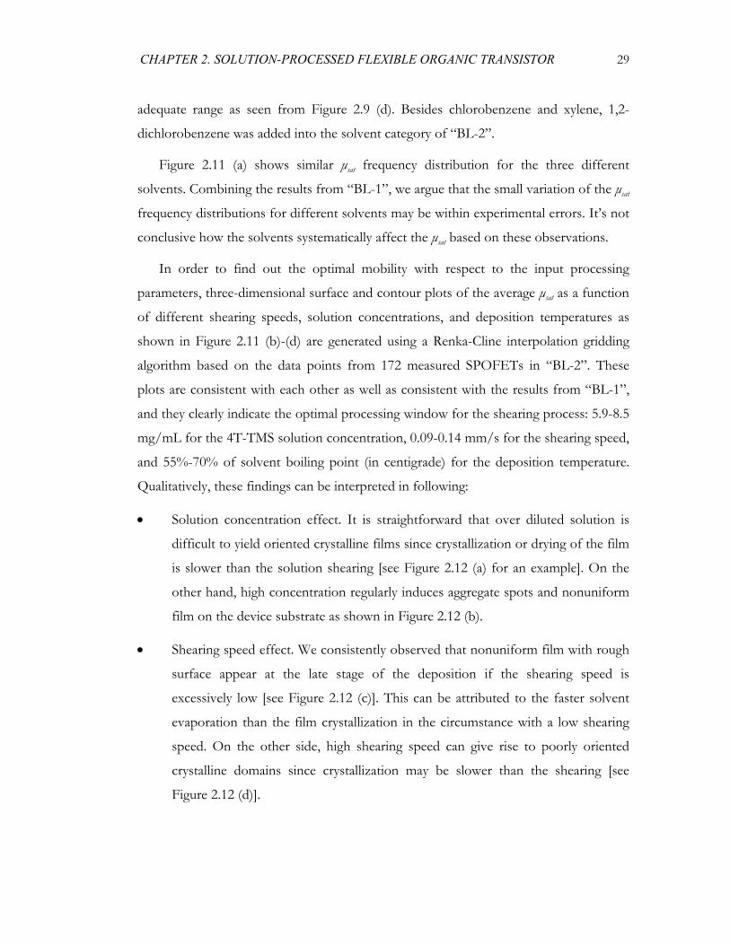
CHAPTER 2. SOLUTION-PROCESSED FLEXIBLE ORGANIC TRANSISTOR 29
adequate range as seen from Figure 2.9 (d). Besides chlorobenzene and xylene, 1,2-
dichlorobenzene was added into the solvent category of “BL-2”.
Figure 2.11 (a) shows similar μsat frequency distribution for the three different
solvents. Combining the results from “BL-1”, we argue that the small variation of the μsat
frequency distributions for different solvents may be within experimental errors. It’s not
conclusive how the solvents systematically affect the μsat based on these observations.
In order to find out the optimal mobility with respect to the input processing
parameters, three-dimensional surface and contour plots of the average μsat as a function
of different shearing speeds, solution concentrations, and deposition temperatures as
shown in Figure 2.11 (b)-(d) are generated using a Renka-Cline interpolation gridding
algorithm based on the data points from 172 measured SPOFETs in “BL-2”. These
plots are consistent with each other as well as consistent with the results from “BL-1”,
and they clearly indicate the optimal processing window for the shearing process: 5.9-8.5
mg/mL for the 4T-TMS solution concentration, 0.09-0.14 mm/s for the shearing speed,
and 55%-70% of solvent boiling point (in centigrade) for the deposition temperature.
Qualitatively, these findings can be interpreted in following:
• Solution concentration effect. It is straightforward that over diluted solution is
difficult to yield oriented crystalline films since crystallization or drying of the film
is slower than the solution shearing [see Figure 2.12 (a) for an example]. On the
other hand, high concentration regularly induces aggregate spots and nonuniform
film on the device substrate as shown in Figure 2.12 (b).
• Shearing speed effect. We consistently observed that nonuniform film with rough
surface appear at the late stage of the deposition if the shearing speed is
excessively low [see Figure 2.12 (c)]. This can be attributed to the faster solvent
evaporation than the film crystallization in the circumstance with a low shearing
speed. On the other side, high shearing speed can give rise to poorly oriented
crystalline domains since crystallization may be slower than the shearing [see
Figure 2.12 (d)].
30 CHAPTER 2. SOLUTION-PROCESSED FLEXIBLE ORGANIC TRANSISTOR
Figure 2.11 (a) The frequency distribution of μsat for the three different solvents used in “BL-2”. Spline interpolation algorithm is employed to generate the curves to facilitate comparison. (b)-(d) Three-dimensional surface and contour plots of the average mobility (μsat) as a function of different shearing speeds, solution concentrations, and deposition temperatures. Here we applied Renka-Cline interpolation gridding algorithm and experimental data points of 172 SPOFETs in “BL-2” for the plotting.
CHAPTER 2. SOLUTION-PROCESSED FLEXIBLE ORGANIC TRANSISTOR 31
Figure 2.12 (a)-(b) Solution concentration effect, (c)-(d) shearing speed effect; and (e)-(f) deposition temperature effect in the solution shearing process, as revealed by the bright-field or cross-polarized microscopy images.
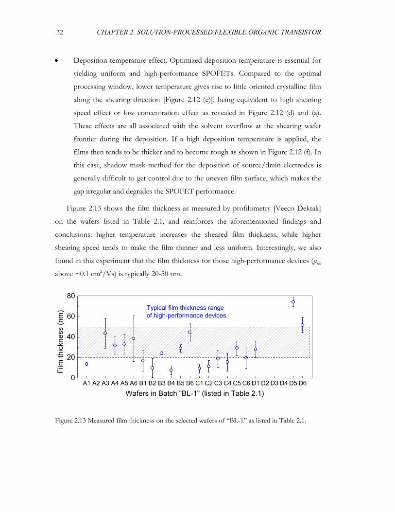
32 CHAPTER 2. SOLUTION-PROCESSED FLEXIBLE ORGANIC TRANSISTOR
• Deposition temperature effect. Optimized deposition temperature is essential for
yielding uniform and high-performance SPOFETs. Compared to the optimal
processing window, lower temperature gives rise to little oriented crystalline film
along the shearing direction [Figure 2.12 (e)], being equivalent to high shearing
speed effect or low concentration effect as revealed in Figure 2.12 (d) and (a).
These effects are all associated with the solvent overflow at the shearing wafer
frontier during the deposition. If a high deposition temperature is applied, the
films then tends to be thicker and to become rough as shown in Figure 2.12 (f). In
this case, shadow mask method for the deposition of source/drain electrodes is
generally difficult to get control due to the uneven film surface, which makes the
gap irregular and degrades the SPOFET performance.
Figure 2.13 shows the film thickness as measured by profilometry [Veeco Dektak]
on the wafers listed in Table 2.1, and reinforces the aforementioned findings and
conclusions: higher temperature increases the sheared film thickness, while higher
shearing speed tends to make the film thinner and less uniform. Interestingly, we also
found in this experiment that the film thickness for those high-performance devices (μsat
above ~0.1 cm2/Vs) is typically 20-50 nm.
A1 A2 A3 A4 A5 A6 B1 B2 B3 B4 B5 B6 C1 C2 C3 C4 C5 C6 D1 D2 D3 D4 D5 D60
20
40
60
80
Film
thic
knes
s (n
m)
Wafers in Batch "BL-1" (listed in Table 2.1)
Typical film thickness range of high-performance devices
Figure 2.13 Measured film thickness on the selected wafers of “BL-1” as listed in Table 2.1.
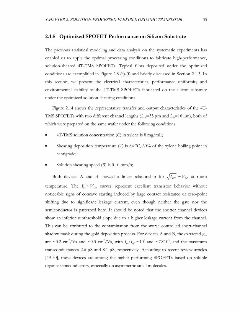
CHAPTER 2. SOLUTION-PROCESSED FLEXIBLE ORGANIC TRANSISTOR 33
2.1.5 Optimized SPOFET Performance on Silicon Substrate
The previous statistical modeling and data analysis on the systematic experiments has
enabled us to apply the optimal processing conditions to fabricate high-performance,
solution-sheared 4T-TMS SPOFETs. Typical films deposited under the optimized
conditions are exemplified in Figure 2.8 (e)-(f) and briefly discussed in Section 2.1.3. In
this section, we present the electrical characteristics, performance uniformity and
environmental stability of the 4T-TMS SPOFETs fabricated on the silicon substrate
under the optimized solution-shearing conditions.
Figure 2.14 shows the representative transfer and output characteristics of the 4T-
TMS SPOFETs with two different channel lengths (LA=35 μm and LB=16 μm), both of
which were prepared on the same wafer under the following conditions:
• 4T-TMS solution concentration (C) in xylene is 8 mg/mL;
• Shearing deposition temperature (T) is 84 ºC, 60% of the xylene boiling point in
centigrade;
• Solution shearing speed (R) is 0.10 mm/s;
Both devices A and B showed a linear relationship for DSI ~VGS at room
temperature. The IDS~VDS curves represent excellent transistor behavior without
noticeable signs of concave starting induced by large contact resistance or zero-point
shifting due to significant leakage current, even though neither the gate nor the
semiconductor is patterned here. It should be noted that the shorter channel devices
show an inferior subthreshold slope due to a higher leakage current from the channel.
This can be attributed to the contamination from the worse controlled short-channel
shadow mask during the gold deposition process. For devices A and B, the extracted μsat
are ~0.2 cm2/Vs and ~0.3 cm2/Vs, with Ion/Ioff ~106 and ~7×10⁵, and the maximum
transconductances 2.6 μS and 8.1 μS, respectively. According to recent review articles
[49-50], these devices are among the higher performing SPOFETs based on soluble
organic semiconductors, especially on asymmetric small molecules.
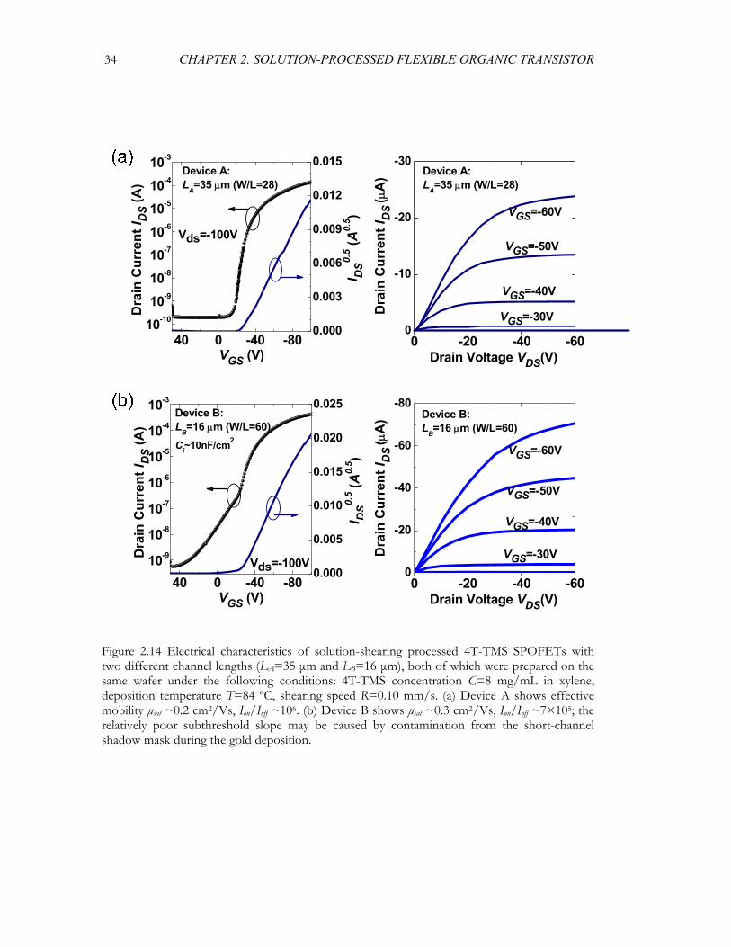
34 CHAPTER 2. SOLUTION-PROCESSED FLEXIBLE ORGANIC TRANSISTOR
40 0 -40 -8010-10
10-9
10-8
10-7
10-6
10-5
10-4
10-3
VGS (V)
Dra
in C
urre
nt I D
S (A
)
0.000
0.003
0.006
0.009
0.012
0.015Device A: LA=35 μm (W/L=28)
I DS0.
5 (A0.
5 )
Vds=-100V
0 -20 -40 -600
-10
-20
-30
D
rain
Cur
rent
I DS
(μA
)Drain Voltage VDS(V)
VGS=-60V
VGS=-50V
VGS=-40V
VGS=-30V
Device A: LA=35 μm (W/L=28)
40 0 -40 -8010-9
10-8
10-7
10-6
10-5
10-4
10-3
Ci~10nF/cm2
VGS (V)
Dra
in C
urre
nt I D
S (A
)
0.000
0.005
0.010
0.015
0.020
0.025Device B: LB=16 μm (W/L=60)
I DS0.
5 (A0.
5 )
Vds=-100V0 -20 -40 -60
0
-20
-40
-60
-80
Dra
in C
urre
nt I D
S (μ
A)
Drain Voltage VDS(V)
VGS=-60V
VGS=-50V
VGS=-40V
VGS=-30V
Device B: LB=16 μm (W/L=60)
Figure 2.14 Electrical characteristics of solution-shearing processed 4T-TMS SPOFETs with two different channel lengths (LA=35 μm and LB=16 μm), both of which were prepared on the same wafer under the following conditions: 4T-TMS concentration C=8 mg/mL in xylene, deposition temperature T=84 ºC, shearing speed R=0.10 mm/s. (a) Device A shows effective mobility μsat ~0.2 cm2/Vs, Ion/Ioff ~106. (b) Device B shows μsat ~0.3 cm2/Vs, Ion/Ioff ~7×10⁵; the relatively poor subthreshold slope may be caused by contamination from the short-channel shadow mask during the gold deposition.
CHAPTER 2. SOLUTION-PROCESSED FLEXIBLE ORGANIC TRANSISTOR 35
To understand our SPOFET performance uniformity under a specific processing
condition, we plot in Figure 2.15 the mobility and Ion/Ioff distribution of 18 measured
samples on the same wafer as devices A and B. These devices, with channel lengths of
13-50 μm and channel widths of 960-1000 μm, show an overall μsat=0.20±0.06 cm2/Vs
and an average Ion/Ioff>106.
0.05 0.10 0.15 0.20 0.25 0.30 0.35 0.400
15
30
45
60 Gaussian Fit
Freq
uenc
y (%
)
Effective Mobility µsat (cm2/Vs)
0
20
40
60
80 Gaussian Fit
1010103
Freq
uenc
y (%
)
Ion/Ioff102 105104 109108107106
Figure 2.15 The effective saturation mobility (μsat) and Ion/Ioff distribution of 18 measured samples fabricated on the same wafer as for devices A and B shown in Figure 2.14. The red line is based on the Gaussian fitting model.
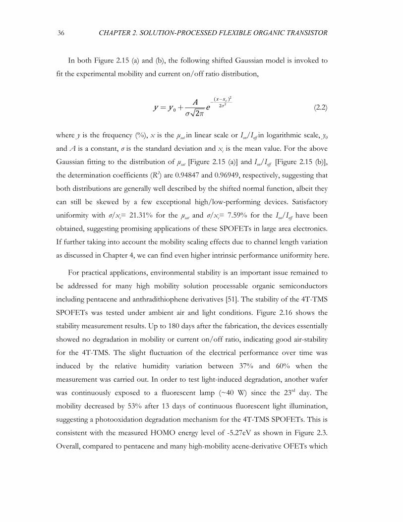
36 CHAPTER 2. SOLUTION-PROCESSED FLEXIBLE ORGANIC TRANSISTOR
In both Figure 2.15 (a) and (b), the following shifted Gaussian model is invoked to
fit the experimental mobility and current on/off ratio distribution,
2
220 2
cx xAy y e σ
σ π
−−= + (2.2)
where y is the frequency (%), x is the μsat in linear scale or Ion/Ioff in logarithmic scale, y0
and A is a constant, σ is the standard deviation and xc is the mean value. For the above
Gaussian fitting to the distribution of μsat [Figure 2.15 (a)] and Ion/Ioff [Figure 2.15 (b)],
the determination coefficients (R2) are 0.94847 and 0.96949, respectively, suggesting that
both distributions are generally well described by the shifted normal function, albeit they
can still be skewed by a few exceptional high/low-performing devices. Satisfactory
uniformity with σ/xc= 21.31% for the μsat and σ/xc= 7.59% for the Ion/Ioff have been
obtained, suggesting promising applications of these SPOFETs in large area electronics.
If further taking into account the mobility scaling effects due to channel length variation
as discussed in Chapter 4, we can find even higher intrinsic performance uniformity here.
For practical applications, environmental stability is an important issue remained to
be addressed for many high mobility solution processable organic semiconductors
including pentacene and anthradithiophene derivatives [51]. The stability of the 4T-TMS
SPOFETs was tested under ambient air and light conditions. Figure 2.16 shows the
stability measurement results. Up to 180 days after the fabrication, the devices essentially
showed no degradation in mobility or current on/off ratio, indicating good air-stability
for the 4T-TMS. The slight fluctuation of the electrical performance over time was
induced by the relative humidity variation between 37% and 60% when the
measurement was carried out. In order to test light-induced degradation, another wafer
was continuously exposed to a fluorescent lamp (~40 W) since the 23rd day. The
mobility decreased by 53% after 13 days of continuous fluorescent light illumination,
suggesting a photooxidation degradation mechanism for the 4T-TMS SPOFETs. This is
consistent with the measured HOMO energy level of -5.27eV as shown in Figure 2.3.
Overall, compared to pentacene and many high-mobility acene-derivative OFETs which
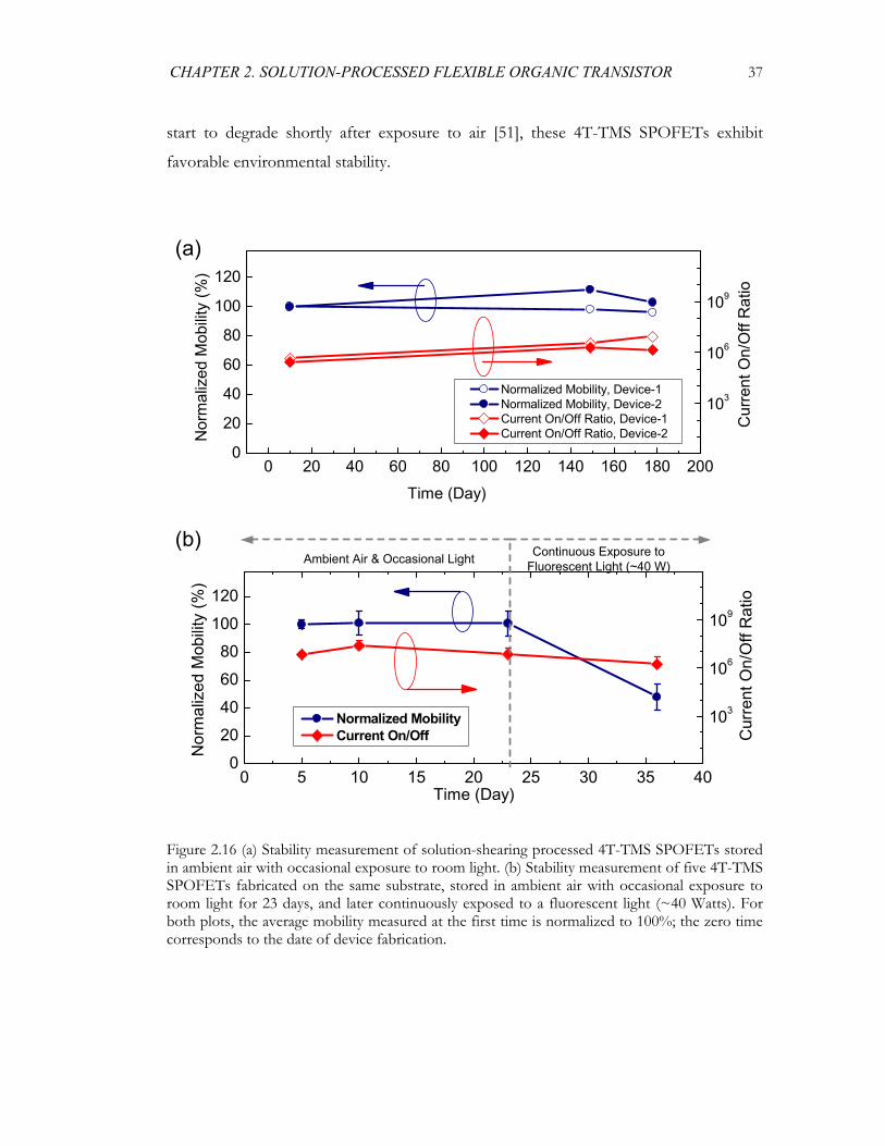
CHAPTER 2. SOLUTION-PROCESSED FLEXIBLE ORGANIC TRANSISTOR 37
start to degrade shortly after exposure to air [51], these 4T-TMS SPOFETs exhibit
favorable environmental stability.
(a)
0 20 40 60 80 100 120 140 160 180 2000
20
40
60
80
100
120
Cur
rent
On/
Off
Rat
io
Time (Day)
Nor
mal
ized
Mob
ility
(%)
Normalized Mobility, Device-1 Normalized Mobility, Device-2 Current On/Off Ratio, Device-1 Current On/Off Ratio, Device-2
103
106
109
(b)
0 5 10 15 20 25 30 35 400
20
40
60
80
100
120
Normalized Mobility Current On/Off
Time (Day)
Nor
mal
ized
Mob
ility
(%)
103
106
109
Cur
rent
On/
Off
Rat
io
Ambient Air & Occasional Light Continuous Exposure to Fluorescent Light (~40 W)
Figure 2.16 (a) Stability measurement of solution-shearing processed 4T-TMS SPOFETs stored in ambient air with occasional exposure to room light. (b) Stability measurement of five 4T-TMS SPOFETs fabricated on the same substrate, stored in ambient air with occasional exposure to room light for 23 days, and later continuously exposed to a fluorescent light (~40 Watts). For both plots, the average mobility measured at the first time is normalized to 100%; the zero time corresponds to the date of device fabrication.
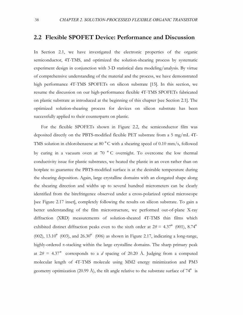
38 CHAPTER 2. SOLUTION-PROCESSED FLEXIBLE ORGANIC TRANSISTOR
2.2 Flexible SPOFET Device: Performance and Discussion
In Section 2.1, we have investigated the electronic properties of the organic
semiconductor, 4T-TMS, and optimized the solution-shearing process by systematic
experiment design in conjunction with 3-D statistical data modeling/analysis. By virtue
of comprehensive understanding of the material and the process, we have demonstrated
high performance 4T-TMS SPOFETs on silicon substrate [15]. In this section, we
resume the discussion on our high-performance flexible 4T-TMS SPOFETs fabricated
on plastic substrate as introduced at the beginning of this chapter [see Section 2.1]. The
optimized solution-shearing process for devices on silicon substrate has been
successfully applied to their counterparts on plastic.
For the flexible SPOFETs shown in Figure 2.2, the semiconductor film was
deposited directly on the PBTS-modified flexible PET substrate from a 5 mg/mL 4T-
TMS solution in chlorobenzene at 80 ºC with a shearing speed of 0.10 mm/s, followed
by curing in a vacuum oven at 70 ºC overnight. To overcome the low thermal
conductivity issue for plastic substrates, we heated the plastic in an oven rather than on
hotplate to guarantee the PBTS-modified surface is at the desirable temperature during
the shearing deposition. Again, large crystalline domains with an elongated shape along
the shearing direction and widths up to several hundred micrometers can be clearly
identified from the birefringence observed under a cross-polarized optical microscope
[see Figure 2.17 inset], completely following the results on silicon substrate. To gain a
better understanding of the film microstructure, we performed out-of-plane X-ray
diffraction (XRD) measurements of solution-sheared 4T-TMS thin films which
exhibited distinct diffraction peaks even to the sixth order at 2θ = 4.37º (001), 8.74º
(002), 13.10º (003), and 26.30º (006) as shown in Figure 2.17, indicating a long-range,
highly-ordered π-stacking within the large crystalline domains. The sharp primary peak
at 2θ = 4.37º corresponds to a d spacing of 20.20 Å. Judging from a computed
molecular length of 4T-TMS molecule using MM2 energy minimization and PM3
geometry optimization (20.99 Å), the tilt angle relative to the substrate surface of 74º is
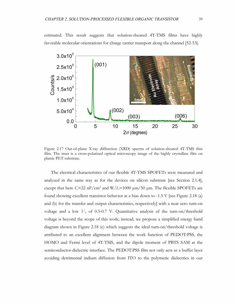
CHAPTER 2. SOLUTION-PROCESSED FLEXIBLE ORGANIC TRANSISTOR 39
estimated. This result suggests that solution-sheared 4T-TMS films have highly
favorable molecular orientations for charge carrier transport along the channel [52-53].
0 5 10 15 20 25 300.0
5.0x10⁴
1.0x10⁵
1.5x10⁵
2.0x10⁵
2.5x10⁵
3.0x10⁵C
ount
s/s
2θ (degrees)
(001)
(002)(003) (006)
Au E
lect
rode
Arr
ay Shea
ring
Figure 2.17 Out-of-plane X-ray diffraction (XRD) spectra of solution-sheared 4T-TMS thin film. The inset is a cross-polarized optical microscopy image of the highly crystalline film on plastic PET substrate.
The electrical characteristics of our flexible 4T-TMS SPOFETs were measured and
analyzed in the same way as for the devices on silicon substrate [see Section 2.1.4],
except that here Ci≈22 nF/cm2 and W/L=1000 μm/50 μm. The flexible SPOFETs are
found showing excellent transistor behavior at a bias down to -1.5 V [see Figure 2.18 (a)
and (b) for the transfer and output characteristics, respectively] with a near zero turn-on
voltage and a low VT of 0.5-0.7 V. Quantitative analysis of the turn-on/threshold
voltage is beyond the scope of this work; instead, we propose a simplified energy band
diagram shown in Figure 2.18 (c) which suggests the ideal turn-on/threshold voltage is
attributed to an excellent alignment between the work function of PEDOT:PSS, the
HOMO and Fermi level of 4T-TMS, and the dipole moment of PBTS SAM at the
semiconductor-dielectric interface. The PEDOT:PSS film not only acts as a buffer layer
avoiding detrimental indium diffusion from ITO to the polymeric dielectrics in our
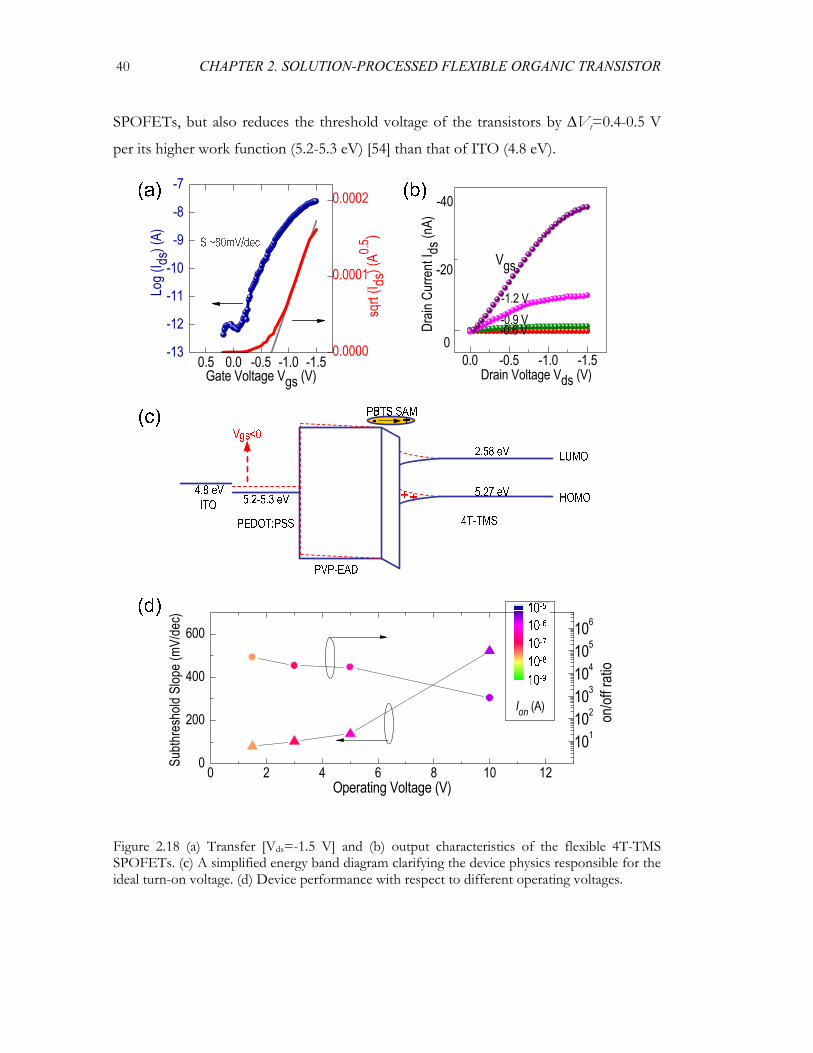
40 CHAPTER 2. SOLUTION-PROCESSED FLEXIBLE ORGANIC TRANSISTOR
SPOFETs, but also reduces the threshold voltage of the transistors by ∆Vt=0.4-0.5 V
per its higher work function (5.2-5.3 eV) [54] than that of ITO (4.8 eV).
0.5 0.0 -0.5 -1.0 -1.5-13
-12
-11
-10
-9
-8
-7
sqrt
(I ds) (
A0.5)
Gate Voltage Vgs (V)
Log (
I ds) (
A) S ~80mV/dec
0.0000
0.0001
0.0002
0.0 -0.5 -1.0 -1.5
Vgs
-0.6 V-0.9 VDr
ain C
urre
nt I ds
(nA)
Drain Voltage Vds (V)
-1.2 V
0
-20
-40
0 2 4 6 8 10 120
200
400
600
Operating Voltage (V)
Subth
resh
old S
lope (
mV/de
c)
1.0E-9
1.0E-8
1.0E-7
1.0E-6
1.0E-5
Ion (A)
101102103104105106
on/of
f rati
o
Figure 2.18 (a) Transfer [Vds=-1.5 V] and (b) output characteristics of the flexible 4T-TMS SPOFETs. (c) A simplified energy band diagram clarifying the device physics responsible for the ideal turn-on voltage. (d) Device performance with respect to different operating voltages.
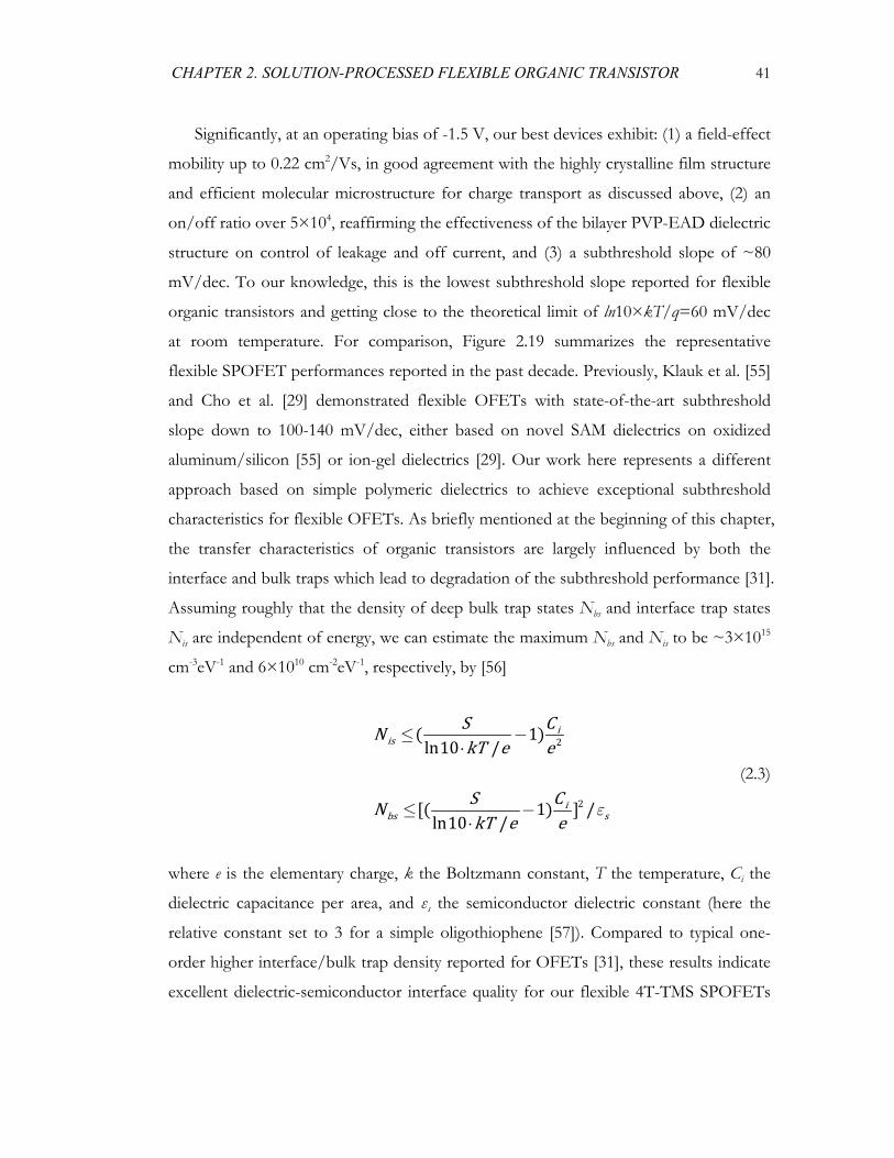
CHAPTER 2. SOLUTION-PROCESSED FLEXIBLE ORGANIC TRANSISTOR 41
Significantly, at an operating bias of -1.5 V, our best devices exhibit: (1) a field-effect
mobility up to 0.22 cm2/Vs, in good agreement with the highly crystalline film structure
and efficient molecular microstructure for charge transport as discussed above, (2) an
on/off ratio over 5×10⁴, reaffirming the effectiveness of the bilayer PVP-EAD dielectric
structure on control of leakage and off current, and (3) a subthreshold slope of ~80
mV/dec. To our knowledge, this is the lowest subthreshold slope reported for flexible
organic transistors and getting close to the theoretical limit of ln10×kT/q=60 mV/dec
at room temperature. For comparison, Figure 2.19 summarizes the representative
flexible SPOFET performances reported in the past decade. Previously, Klauk et al. [55]
and Cho et al. [29] demonstrated flexible OFETs with state-of-the-art subthreshold
slope down to 100-140 mV/dec, either based on novel SAM dielectrics on oxidized
aluminum/silicon [55] or ion-gel dielectrics [29]. Our work here represents a different
approach based on simple polymeric dielectrics to achieve exceptional subthreshold
characteristics for flexible OFETs. As briefly mentioned at the beginning of this chapter,
the transfer characteristics of organic transistors are largely influenced by both the
interface and bulk traps which lead to degradation of the subthreshold performance [31].
Assuming roughly that the density of deep bulk trap states Nbs and interface trap states
Nis are independent of energy, we can estimate the maximum Nbs and Nis to be ~3×10¹⁵
cm-3eV-1 and 6×1010 cm-2eV-1, respectively, by [56]
2
2
1ln10 /
1 /ln10 /
iis
ibs s
S CNkT e e
S CNkT e e
ε
≤ −⋅
≤ −⋅
(2.3)
where e is the elementary charge, k the Boltzmann constant, T the temperature, Ci the
dielectric capacitance per area, and εs the semiconductor dielectric constant (here the
relative constant set to 3 for a simple oligothiophene [57]). Compared to typical one-
order higher interface/bulk trap density reported for OFETs [31], these results indicate
excellent dielectric-semiconductor interface quality for our flexible 4T-TMS SPOFETs
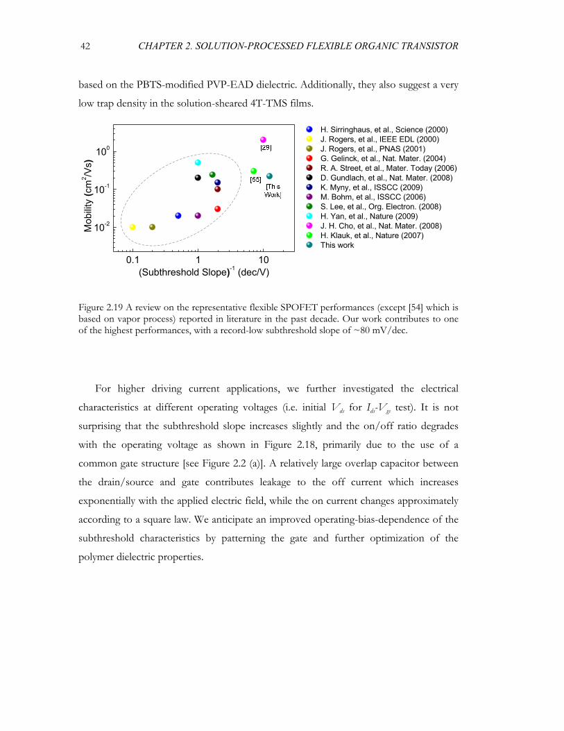
42 CHAPTER 2. SOLUTION-PROCESSED FLEXIBLE ORGANIC TRANSISTOR
based on the PBTS-modified PVP-EAD dielectric. Additionally, they also suggest a very
low trap density in the solution-sheared 4T-TMS films.
0.1 1 10
10-2
10-1
100
H. Sirringhaus, et al., Science (2000) J. Rogers, et al., IEEE EDL (2000) J. Rogers, et al., PNAS (2001) G. Gelinck, et al., Nat. Mater. (2004) R. A. Street, et al., Mater. Today (2006) D. Gundlach, et al., Nat. Mater. (2008) K. Myny, et al., ISSCC (2009) M. Bohm, et al., ISSCC (2006) S. Lee, et al., Org. Electron. (2008) H. Yan, et al., Nature (2009) J. H. Cho, et al., Nat. Mater. (2008) H. Klauk, et al., Nature (2007) This work
Mob
ility
(cm
2 /Vs)
(Subthreshold Slope)-1 (dec/V)
Figure 2.19 A review on the representative flexible SPOFET performances (except [54] which is based on vapor process) reported in literature in the past decade. Our work contributes to one of the highest performances, with a record-low subthreshold slope of ~80 mV/dec.
For higher driving current applications, we further investigated the electrical
characteristics at different operating voltages (i.e. initial Vds for Ids-Vgs test). It is not
surprising that the subthreshold slope increases slightly and the on/off ratio degrades
with the operating voltage as shown in Figure 2.18, primarily due to the use of a
common gate structure [see Figure 2.2 (a)]. A relatively large overlap capacitor between
the drain/source and gate contributes leakage to the off current which increases
exponentially with the applied electric field, while the on current changes approximately
according to a square law. We anticipate an improved operating-bias-dependence of the
subthreshold characteristics by patterning the gate and further optimization of the
polymer dielectric properties.
CHAPTER 2. SOLUTION-PROCESSED FLEXIBLE ORGANIC TRANSISTOR 43
2.3 Summary
We have shown that flexible SPOFETs on rough plastic substrates with a charge carrier
mobility up to 0.22 cm2/Vs, a turn-on voltage of near 0 V, and a record-low
subthreshold slope of ~80 mV/dec are possible in ambient conditions. These
exceptional characteristics are attributed to: (1) a novel device stacking architecture with
a conducting polymeric gate electrode and a double layered dielectric composed of low-
temperature cross-linked poly(4-vinylphenol) (PVP); (2) a low interface trap density
achieved by modifying the PVP dielectric surface with a phenyl-terminated self-
assembled monolayer from 4-phenylbutyltrichlorosilane (PBTS); and (3) controlled
crystallization of a small-molecule organic semiconductor 4T-TMS film with favorable
charge transport microstructure and a low bulk trap density as deposited by a statistically
optimized solution-shearing process.
In addition, we present the systematic experiment design and the corresponding 3-D
statistical modeling/analysis which provides a general guideline for process optimization
for fabricating high-performance SPOFETs.
Future work in this part includes analytical or quantitative modeling for the shearing
process based on evaporation kinetics and crystallization kinetics, enhancing the device
tolerance to higher driving-current operation through gate patterning, and integrating
such SPOFETs in flexible electronic circuits and systems.

44 CHAPTER 2. SOLUTION-PROCESSED FLEXIBLE ORGANIC TRANSISTOR
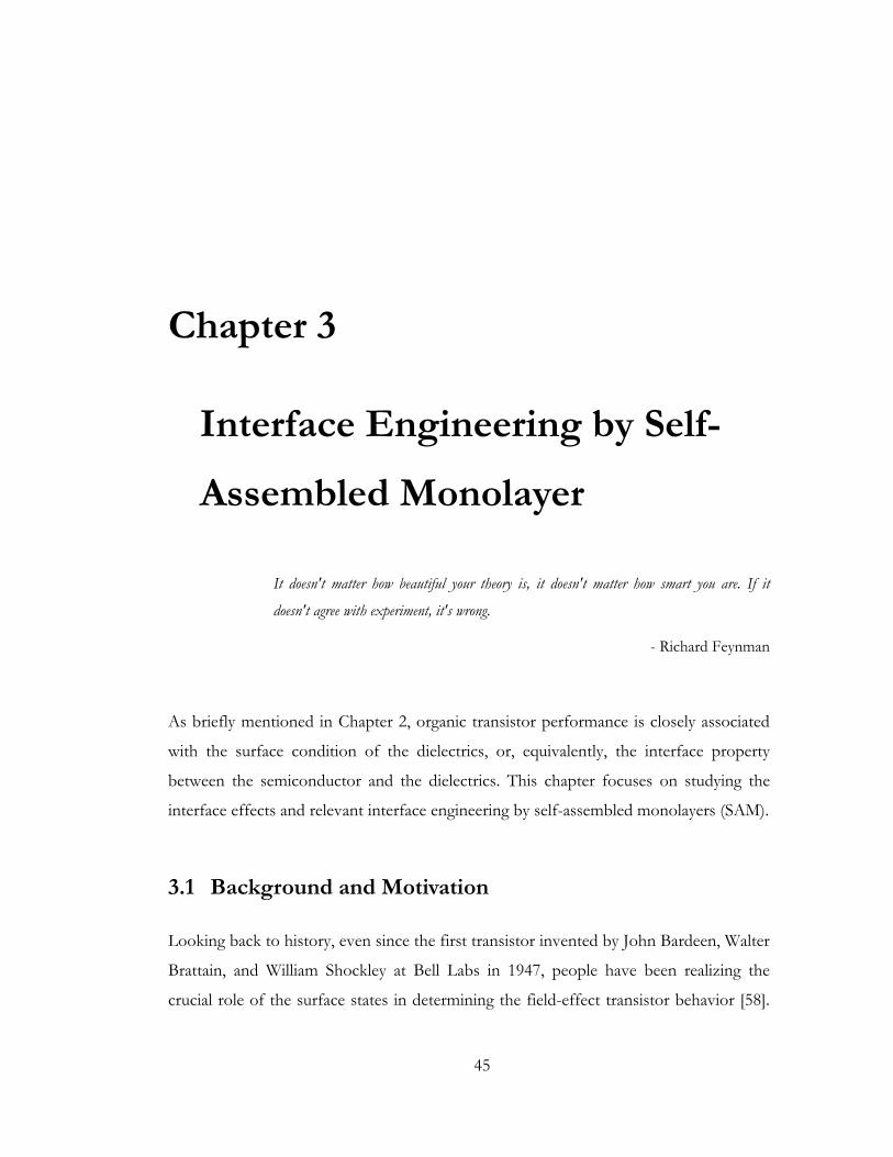
45
Chapter 3
Interface Engineering by Self-
Assembled Monolayer
It doesn't matter how beautiful your theory is, it doesn't matter how smart you are. If it
doesn't agree with experiment, it's wrong.
- Richard Feynman
As briefly mentioned in Chapter 2, organic transistor performance is closely associated
with the surface condition of the dielectrics, or, equivalently, the interface property
between the semiconductor and the dielectrics. This chapter focuses on studying the
interface effects and relevant interface engineering by self-assembled monolayers (SAM).
3.1 Background and Motivation
Looking back to history, even since the first transistor invented by John Bardeen, Walter
Brattain, and William Shockley at Bell Labs in 1947, people have been realizing the
crucial role of the surface states in determining the field-effect transistor behavior [58].
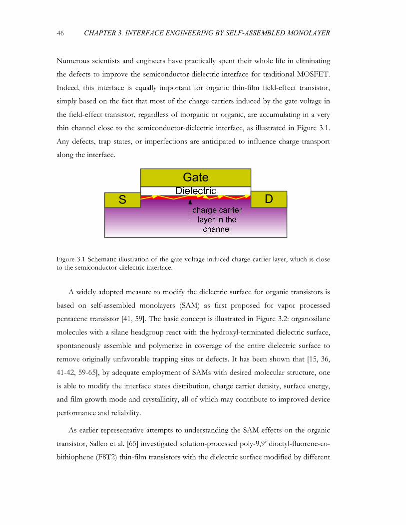
46 CHAPTER 3. INTERFACE ENGINEERING BY SELF-ASSEMBLED MONOLAYER
Numerous scientists and engineers have practically spent their whole life in eliminating
the defects to improve the semiconductor-dielectric interface for traditional MOSFET.
Indeed, this interface is equally important for organic thin-film field-effect transistor,
simply based on the fact that most of the charge carriers induced by the gate voltage in
the field-effect transistor, regardless of inorganic or organic, are accumulating in a very
thin channel close to the semiconductor-dielectric interface, as illustrated in Figure 3.1.
Any defects, trap states, or imperfections are anticipated to influence charge transport
along the interface.
Figure 3.1 Schematic illustration of the gate voltage induced charge carrier layer, which is close to the semiconductor-dielectric interface.
A widely adopted measure to modify the dielectric surface for organic transistors is
based on self-assembled monolayers (SAM) as first proposed for vapor processed
pentacene transistor [41, 59]. The basic concept is illustrated in Figure 3.2: organosilane
molecules with a silane headgroup react with the hydroxyl-terminated dielectric surface,
spontaneously assemble and polymerize in coverage of the entire dielectric surface to
remove originally unfavorable trapping sites or defects. It has been shown that [15, 36,
41-42, 59-65], by adequate employment of SAMs with desired molecular structure, one
is able to modify the interface states distribution, charge carrier density, surface energy,
and film growth mode and crystallinity, all of which may contribute to improved device
performance and reliability.
As earlier representative attempts to understanding the SAM effects on the organic
transistor, Salleo et al. [65] investigated solution-processed poly-9,9’ dioctyl-fluorene-co-
bithiophene (F8T2) thin-film transistors with the dielectric surface modified by different
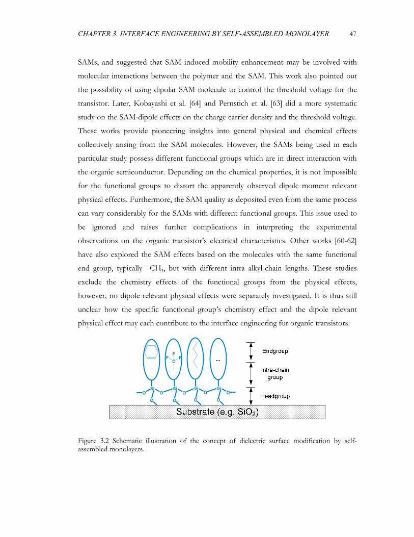
CHAPTER 3. INTERFACE ENGINEERING BY SELF-ASSEMBLED MONOLAYER 47
SAMs, and suggested that SAM induced mobility enhancement may be involved with
molecular interactions between the polymer and the SAM. This work also pointed out
the possibility of using dipolar SAM molecule to control the threshold voltage for the
transistor. Later, Kobayashi et al. [64] and Pernstich et al. [63] did a more systematic
study on the SAM-dipole effects on the charge carrier density and the threshold voltage.
These works provide pioneering insights into general physical and chemical effects
collectively arising from the SAM molecules. However, the SAMs being used in each
particular study possess different functional groups which are in direct interaction with
the organic semiconductor. Depending on the chemical properties, it is not impossible
for the functional groups to distort the apparently observed dipole moment relevant
physical effects. Furthermore, the SAM quality as deposited even from the same process
can vary considerably for the SAMs with different functional groups. This issue used to
be ignored and raises further complications in interpreting the experimental
observations on the organic transistor’s electrical characteristics. Other works [60-62]
have also explored the SAM effects based on the molecules with the same functional
end group, typically –CH3, but with different intra alkyl-chain lengths. These studies
exclude the chemistry effects of the functional groups from the physical effects,
however, no dipole relevant physical effects were separately investigated. It is thus still
unclear how the specific functional group’s chemistry effect and the dipole relevant
physical effect may each contribute to the interface engineering for organic transistors.
SiO
OO
Si
OO
Si
OO
Si
OO
CFF
F
Figure 3.2 Schematic illustration of the concept of dielectric surface modification by self-assembled monolayers.
48 CHAPTER 3. INTERFACE ENGINEERING BY SELF-ASSEMBLED MONOLAYER
In this work, through careful selection of a group of phenyl-terminated SAMs, we
manage to decouple the dipole moment relevant physical effect from the surface
chemistry effect of the functional groups, to elucidate how the performance and
reliability of organic transistors are controlled by interfacial SAMs [66-67].
The chemical structures of the phenyl-SAM molecules used for this study are shown
in Figure 3.3. The major distinctions of this study are highlighted below:
PTS PETS PBTS PHTS PAPTS
Si O
OO
NH
Si ClCl
ClSi Cl
Cl
Cl Si
Cl
Cl Cl SiClCl
Cl
Figure 3.3 A group of phenyl-terminated SAM molecules used for the interface engineering study in this work. The intra alkyl chain length increases from PTS, PETS, PBTS, to PHTS, PAPTS is comparable to PBTS except that an –NH- group replaces a –CH2- in the intra part of PBTS. (PTS: phenyltrichlorosilane, PETS: phenethyltrichlorosilane, PBTS: 4-phenylbutyltrichlorosilane, PHTS: 6-phenylhexyltrichlorosilane, PAPTS: N-phenylaminopropyltricholorosilane)
• As introduced in Chapter 2 [see Figure 2.5], phenyl-terminated SAMs are
particularly favorable for SPOFETs and can be superior to other SAMs including
the methyl-terminated OTS which is widely used for vapor processed organic
transistors. Therefore, comprehensive understanding of the phenyl-terminated
SAM effects will enable us to further improve the SPOFET performance;
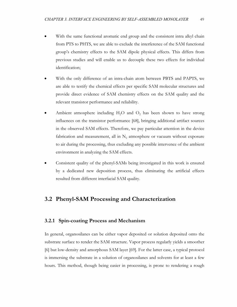
CHAPTER 3. INTERFACE ENGINEERING BY SELF-ASSEMBLED MONOLAYER 49
• With the same functional aromatic end group and the consistent intra alkyl chain
from PTS to PHTS, we are able to exclude the interference of the SAM functional
group’s chemistry effects to the SAM dipole physical effects. This differs from
previous studies and will enable us to decouple these two effects for individual
identification;
• With the only difference of an intra-chain atom between PBTS and PAPTS, we
are able to testify the chemical effects per specific SAM molecular structures and
provide direct evidence of SAM chemistry effects on the SAM quality and the
relevant transistor performance and reliability.
• Ambient atmosphere including H2O and O2 has been shown to have strong
influences on the transistor performance [68], bringing additional artifact sources
in the observed SAM effects. Therefore, we pay particular attention in the device
fabrication and measurement, all in N2 atmosphere or vacuum without exposure
to air during the processing, thus excluding any possible intervence of the ambient
environment in analyzing the SAM effects.
• Consistent quality of the phenyl-SAMs being investigated in this work is ensured
by a dedicated new deposition process, thus eliminating the artificial effects
resulted from different interfacial SAM quality.
3.2 Phenyl-SAM Processing and Characterization
3.2.1 Spin-coating Process and Mechanism
In general, organosilanes can be either vapor deposited or solution deposited onto the
substrate surface to render the SAM structure. Vapor process regularly yields a smoother
[6] but low-density and amorphous SAM layer [69]. For the latter case, a typical protocol
is immersing the substrate in a solution of organosilanes and solvents for at least a few
hours. This method, though being easier in processing, is prone to rendering a rough
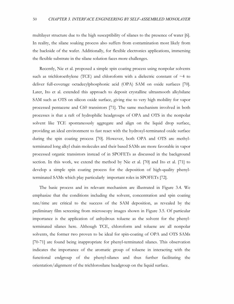
50 CHAPTER 3. INTERFACE ENGINEERING BY SELF-ASSEMBLED MONOLAYER
multilayer structure due to the high susceptibility of silanes to the presence of water [6].
In reality, the silane soaking process also suffers from contamination most likely from
the backside of the wafer. Additionally, for flexible electronics applications, immersing
the flexible substrate in the silane solution faces more challenges.
Recently, Nie et al. proposed a simple spin coating process using nonpolar solvents
such as trichloroethylene (TCE) and chloroform with a dielectric constant of ~4 to
deliver full-coverage octadecylphosphonic acid (OPA) SAM on oxide surfaces [70].
Later, Ito et al. extended this approach to deposit crystalline ultrasmooth alkylsilane
SAM such as OTS on silicon oxide surface, giving rise to very high mobility for vapor
processed pentacene and C60 transistors [71]. The same mechanism involved in both
processes is that a raft of hydrophilic headgroups of OPA and OTS in the nonpolar
solvent like TCE spontaneously aggregate and align on the liquid drop surface,
providing an ideal environment to fast react with the hydroxyl-terminated oxide surface
during the spin coating process [70]. However, both OPA and OTS are methyl-
terminated long alkyl chain molecules and their based SAMs are more favorable in vapor
processed organic transistors instead of in SPOFETs as discussed in the background
section. In this work, we extend the method by Nie et al. [70] and Ito et al. [71] to
develop a simple spin coating process for the deposition of high-quality phenyl-
terminated SAMs which play particularly important roles in SPOFETs [72].
The basic process and its relevant mechanism are illustrated in Figure 3.4. We
emphasize that the conditions including the solvent, concentration and spin coating
rate/time are critical to the success of the SAM deposition, as revealed by the
preliminary film screening from microscopy images shown in Figure 3.5. Of particular
importance is the application of anhydrous toluene as the solvent for the phenyl-
terminated silanes here. Although TCE, chloroform and toluene are all nonpolar
solvents, the former two proven to be ideal for spin-coating of OPA and OTS SAMs
[70-71] are found being inappropriate for phenyl-terminated silanes. This observation
indicates the importance of the aromatic group of toluene in interacting with the
functional endgroup of the phenyl-silanes and thus further facilitating the
orientation/alignment of the trichlorosilane headgroup on the liquid surface.
CHAPTER 3. INTERFACE ENGINEERING BY SELF-ASSEMBLED MONOLAYER 51
Figure 3.4 Schematic illustration of the spin-coating process for depositing phenyl-terminated SAMs from the solution of phenyl-trichlorosilane in anhydrous toluene. The trichlorosilane headgroup spontaneously aggregate and align on the liquid drop surface, providing an ideal environment for the fast reaction of the trichlorosilane with the hydroxyl group on the substrate surface [70-71]. The anhydrous toluene solvent being selected here is critical to the process. The conjugated aromatic group of toluene is supposed to interact with the functional endgroup of the phenyl-silane and facilitate the alignment of the phenyl-silane on the liquid drop surface.
Figure 3.5 A preliminary screening of different film morphology as deposited by different spin-coating processes for PBTS. Images were taken under bright-field microscope. The solvent, concentration and spin rate/time are all critical to high quality phenyl-SAM.
52 CHAPTER 3. INTERFACE ENGINEERING BY SELF-ASSEMBLED MONOLAYER
The aligned tricholorsilane headgroup on the liquid surface reacts fast with the
hydroxyl group on the substrate surface and the excessive solution is removed during
the spin process. Subsequent post-processing by treating the spin-coated substrates in
hydrochloric acid vapor for overnight is necessary to allow further hydrolysis and
siloxane polymerization on the surface. The optimized process details are given in the
Appendix section in this dissertation.
3.2.2 Spin-coated Phenyl-SAM Characterization
The phenyl-terminated SAMs as deposited by the same optimized spin-coating process
are characterized by techniques including water contact angle (CA), atomic force
microscopy (AFM), ellipsometry, and grazing incidence X-ray diffraction (GIXD).
Figure 3.6 shows the measured water contact angle [Edmund Scientific goniometer] on
each phenyl-SAM modified SiO2 surface. For PTS, PETS, PBTS, and PHTS with similar
molecular structure, the water contact angle increases monotonically with the intra-alkyl-
chain length from ~70º to ~90º, indicating relatively low surface energy and high density
of the SAMs as deposited by the spin coating process. For PAPTS which contains a -
NH- in the intra-chain, a lower contact angle is observed over the comparable PBTS
where only -CH2- appears in the chain. This effect may arise from the SAM morphology
difference as induced by the molecular structures during the spin coating process, and
the stronger dipolar interaction between the PAPTS SAM and the polar water molecule.
As shown in Figure 3.7, AFM measurement [Veeco Nanoscope] reveals that the
phenyl-terminated SAMs as deposited by the optimized spin-coating process are
generally showing remarkably high degree of smoothness, with typical roughness of 0.1-
0.2 nm (rms) for PTS/PETS/PBTS/PHTS and 0.2-0.3 nm (rms) for PAPTS. No
appreciable difference among the morphology of PTS/PETS/PBTS/PHTS SAMs is
observed. However, a relatively rougher film surface is found for PAPTS, indicating the
SAM molecular structure with specific chemical functional groups in affecting the SAM
quality even based on the same process. This underscores the importance of selecting
appropriate SAM structures in studying the SAM effects for organic electronic devices.
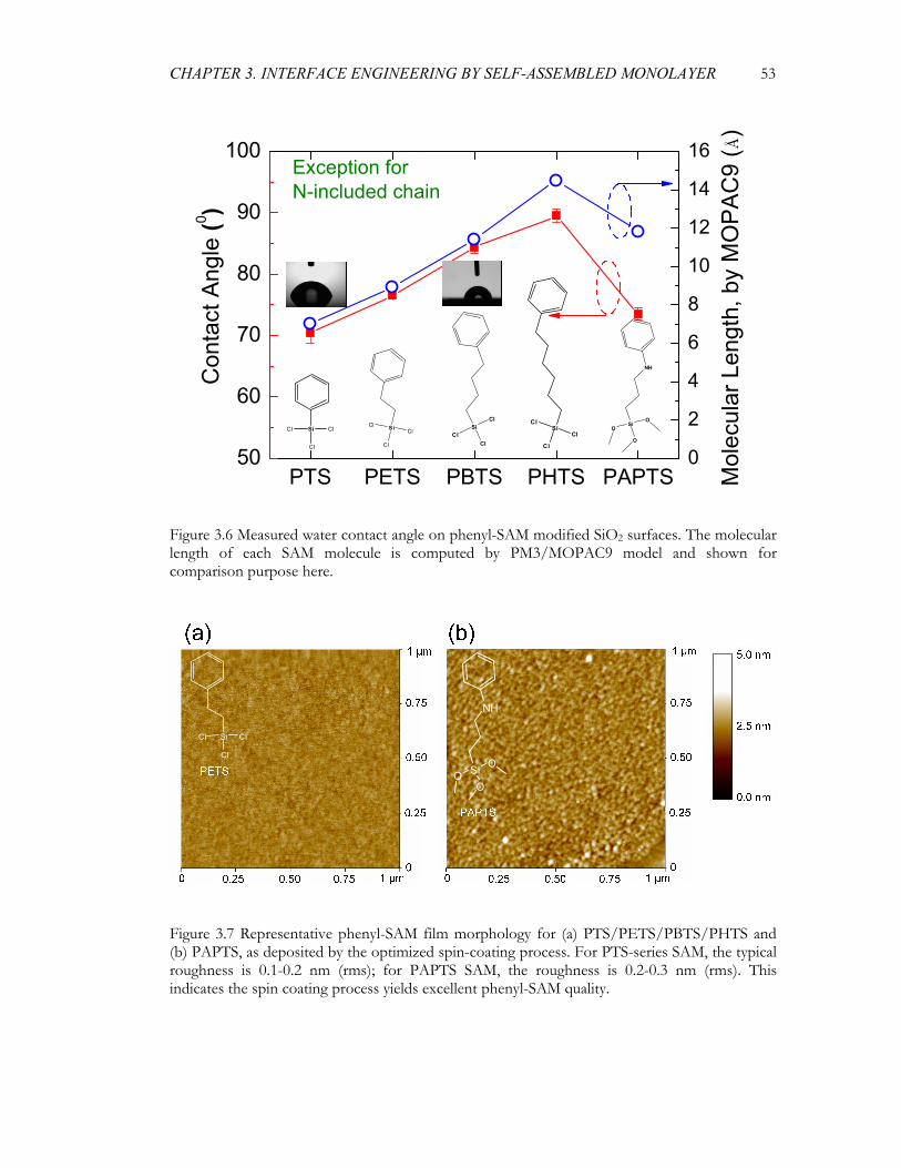
CHAPTER 3. INTERFACE ENGINEERING BY SELF-ASSEMBLED MONOLAYER 53
PTS PETS PBTS PHTS PAPTS50
60
70
80
90
100
Mol
ecul
ar L
engt
h, b
y M
OPA
C9
(Å)
Con
tact
Ang
le (0 )
Si
Cl
Cl Cl Si
Cl
ClCl
SiO
O
O
NH
SiCl
Cl
Cl
SiCl
Cl
Cl
Exception for N-included chain
0
2
4
6
8
10
12
14
16
Figure 3.6 Measured water contact angle on phenyl-SAM modified SiO2 surfaces. The molecular length of each SAM molecule is computed by PM3/MOPAC9 model and shown for comparison purpose here.
Si
Cl
Cl Cl
Si O
OO
NH
Figure 3.7 Representative phenyl-SAM film morphology for (a) PTS/PETS/PBTS/PHTS and (b) PAPTS, as deposited by the optimized spin-coating process. For PTS-series SAM, the typical roughness is 0.1-0.2 nm (rms); for PAPTS SAM, the roughness is 0.2-0.3 nm (rms). This indicates the spin coating process yields excellent phenyl-SAM quality.
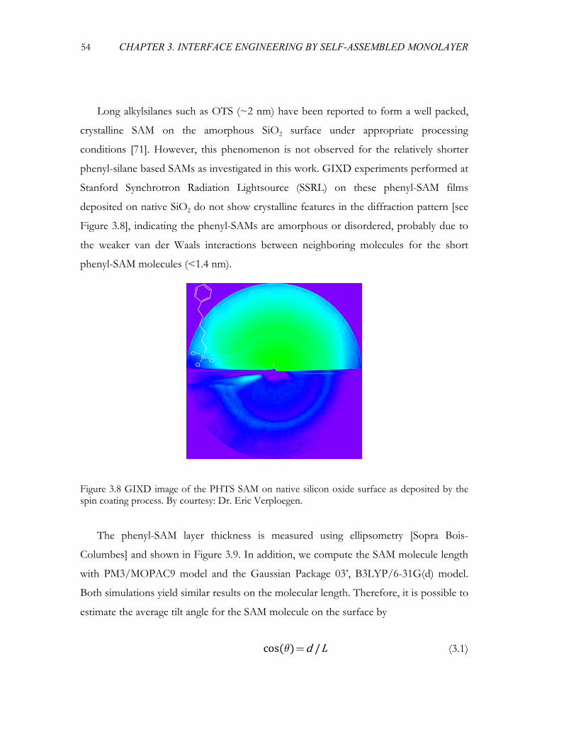
54 CHAPTER 3. INTERFACE ENGINEERING BY SELF-ASSEMBLED MONOLAYER
Long alkylsilanes such as OTS (~2 nm) have been reported to form a well packed,
crystalline SAM on the amorphous SiO2 surface under appropriate processing
conditions [71]. However, this phenomenon is not observed for the relatively shorter
phenyl-silane based SAMs as investigated in this work. GIXD experiments performed at
Stanford Synchrotron Radiation Lightsource (SSRL) on these phenyl-SAM films
deposited on native SiO2 do not show crystalline features in the diffraction pattern [see
Figure 3.8], indicating the phenyl-SAMs are amorphous or disordered, probably due to
the weaker van der Waals interactions between neighboring molecules for the short
phenyl-SAM molecules (<1.4 nm).
SiCl
Cl
Cl
Figure 3.8 GIXD image of the PHTS SAM on native silicon oxide surface as deposited by the spin coating process. By courtesy: Dr. Eric Verploegen.
The phenyl-SAM layer thickness is measured using ellipsometry [Sopra Bois-
Columbes] and shown in Figure 3.9. In addition, we compute the SAM molecule length
with PM3/MOPAC9 model and the Gaussian Package 03’, B3LYP/6-31G(d) model.
Both simulations yield similar results on the molecular length. Therefore, it is possible to
estimate the average tilt angle for the SAM molecule on the surface by
cos /d Lθ = (3.1)
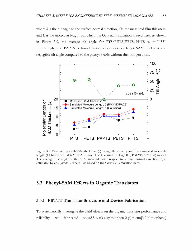
CHAPTER 3. INTERFACE ENGINEERING BY SELF-ASSEMBLED MONOLAYER 55
where θ is the tilt angle to the surface normal direction, d is the measured film thickness,
and L is the molecular length, for which the Gaussian simulation is used here. As shown
in Figure 3.9, the average tilt angle for PTS/PETS/PBTS/PHTS is ~40º-55º.
Interestingly, the PAPTS is found giving a considerably larger SAM thickness and
negligible tilt angle compared to the phenyl-SAMs without the nitrogen atom.
PTS PETS PAPTS PBTS PHTS --0
5
10
15
20
25
30
35
40
-100
-75
-50
-25
0
25
50
75
100
Mol
ecul
ar L
engt
h or
SA
M T
hick
ness
( Å) Measured SAM Thickness, d
Simulated Molecule Length, L (PM3/MOPAC9) Simulated Molecule Length, L (Gaussian)
Tilt
Angl
e, θ
(0 )
cos (θ)= d/L
Figure 3.9 Measured phenyl-SAM thickness (d) using ellipsometry and the simulated molecule length (L) based on PM3/MOPAC9 model or Gaussian Package 03’, B3LYP/6-31G(d) model. The average title angle of the SAM molecule with respect to surface normal direction, θ, is estimated by cos (θ)=d/L, where L is based on the Gaussian simulation here.
3.3 Phenyl-SAM Effects in Organic Transistors
3.3.1 PBTTT Transistor Structure and Device Fabrication
To systematically investigate the SAM effects on the organic transistor performance and
reliability, we fabricated poly(2,5-bis(3-alkylthiophen-2-yl)thieno[3,2-b]thiophene)
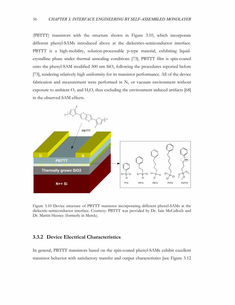
56 CHAPTER 3. INTERFACE ENGINEERING BY SELF-ASSEMBLED MONOLAYER
(PBTTT) transistors with the structure shown in Figure 3.10, which incorporate
different phenyl-SAMs introduced above at the dielectrics-semiconductor interface.
PBTTT is a high-mobility, solution-processable p-type material, exhibiting liquid-
crystalline phase under thermal annealing conditions [73]. PBTTT film is spin-coated
onto the phenyl-SAM modified 300 nm SiO2 following the procedures reported before
[73], rendering relatively high uniformity for its transistor performance. All of the device
fabrication and measurement were performed in N2 or vacuum environment without
exposure to ambient O2 and H2O, thus excluding the environment induced artifacts [68]
in the observed SAM effects.
Thermally grown SiO2
N++ Si
4T-TMS Active LayerD S
PBTTTD S
PTS PETS PBTS PHTS PAPTS
Si O
OO
NH
Si ClCl
ClSi Cl
Cl
Cl Si
Cl
Cl Cl SiClCl
Cl
PBTTT
Figure 3.10 Device structure of PBTTT transistor incorporating different phenyl-SAMs at the dielectric-semiconductor interface. Courtesy: PBTTT was provided by Dr. Iain McCulloch and Dr. Martin Heeney (formerly in Merck).
3.3.2 Device Electrical Characteristics
In general, PBTTT transistors based on the spin-coated phenyl-SAMs exhibit excellent
transistor behavior with satisfactory transfer and output characteristics [see Figure 3.12
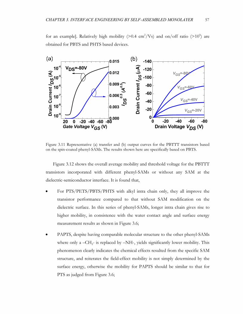
CHAPTER 3. INTERFACE ENGINEERING BY SELF-ASSEMBLED MONOLAYER 57
for an example]. Relatively high mobility (>0.4 cm2/Vs) and on/off ratio (>105) are
obtained for PBTS and PHTS based devices.
20 0 -20 -40 -60 -8010-9
10-8
10-7
10-6
10-5
10-4
Gate Voltage VGS (V)
Dra
in C
urre
nt I D
S (A
)
0.000
0.003
0.006
0.009
0.012
0.015
I DS0.
5 (A0.
5 )
VDS=-80V
0 -20 -40 -60 -800
-20
-40
-60
-80
-100
-120
-140
D
rain
Cur
rent
I DS
(μA
)
Drain Voltage VDS (V)
VGS=-80V
VGS=-60V
VGS=-40V
VGS=-20V
Figure 3.11 Representative (a) transfer and (b) output curves for the PBTTT transistors based on the spin-coated phenyl-SAMs. The results shown here are specifically based on PBTS.
Figure 3.12 shows the overall average mobility and threshold voltage for the PBTTT
transistors incorporated with different phenyl-SAMs or without any SAM at the
dielectric-semiconductor interface. It is found that,
• For PTS/PETS/PBTS/PHTS with alkyl intra chain only, they all improve the
transistor performance compared to that without SAM modification on the
dielectric surface. In this series of phenyl-SAMs, longer intra chain gives rise to
higher mobility, in consistence with the water contact angle and surface energy
measurement results as shown in Figure 3.6;
• PAPTS, despite having comparable molecular structure to the other phenyl-SAMs
where only a –CH2- is replaced by –NH-, yields significantly lower mobility. This
phenomenon clearly indicates the chemical effects resulted from the specific SAM
structure, and reiterates the field-effect mobility is not simply determined by the
surface energy, otherwise the mobility for PAPTS should be similar to that for
PTS as judged from Figure 3.6;
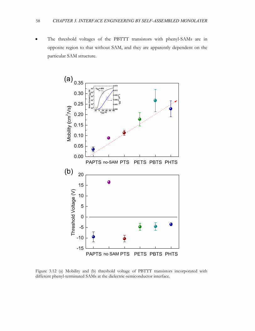
58 CHAPTER 3. INTERFACE ENGINEERING BY SELF-ASSEMBLED MONOLAYER
• The threshold voltages of the PBTTT transistors with phenyl-SAMs are in
opposite region to that without SAM, and they are apparently dependent on the
particular SAM structure.
PAPTS SiO2 PTS PETS PBTS PHTS0.00
0.05
0.10
0.15
0.20
0.25
0.30
0.35
Mob
ility
(cm
2 /Vs)
no-SAM
PAPTS SiO2 PTS PETS PBTS PHTS-15
-10
-5
0
5
10
15
20
Thre
shol
d Vo
ltage
(V)
no SAM
20 0 -20 -40 -60 -8010-9
10-8
10-7
10-6
10-5
10-4
VGS (V)
Dra
in C
urre
nt I D
S (A
)
0.000
0.003
0.006
0.009
0.012
0.015
I DS0.
5 (A
0.5 )
Vds=-80V
Figure 3.12 (a) Mobility and (b) threshold voltage of PBTTT transistors incorporated with different phenyl-terminated SAMs at the dielectric-semiconductor interface.
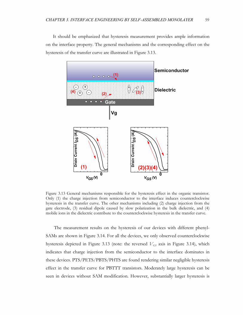
CHAPTER 3. INTERFACE ENGINEERING BY SELF-ASSEMBLED MONOLAYER 59
It should be emphasized that hysteresis measurement provides ample information
on the interface property. The general mechanisms and the corresponding effect on the
hysteresis of the transfer curve are illustrated in Figure 3.13.
VGS (V)
Dra
in C
urre
nt I D
S (A
)
0(1)
VGS (V)
Dra
in C
urre
nt I D
S (A
)
0(2)(3)(4)
Figure 3.13 General mechanisms responsible for the hysteresis effect in the organic transistor. Only (1) the charge injection from semiconductor to the interface induces counterclockwise hysteresis in the transfer curve. The other mechanisms including (2) charge injection from the gate electrode, (3) residual dipole caused by slow polarization in the bulk dielectric, and (4) mobile ions in the dielectric contribute to the counterclockwise hysteresis in the transfer curve.
The measurement results on the hysteresis of our devices with different phenyl-
SAMs are shown in Figure 3.14. For all the devices, we only observed counterclockwise
hysteresis depicted in Figure 3.13 (note: the reversed VGS axis in Figure 3.14), which
indicates that charge injection from the semiconductor to the interface dominates in
these devices. PTS/PETS/PBTS/PHTS are found rendering similar negligible hysteresis
effect in the transfer curve for PBTTT transistors. Moderately large hysteresis can be
seen in devices without SAM modification. However, substantially larger hysteresis is
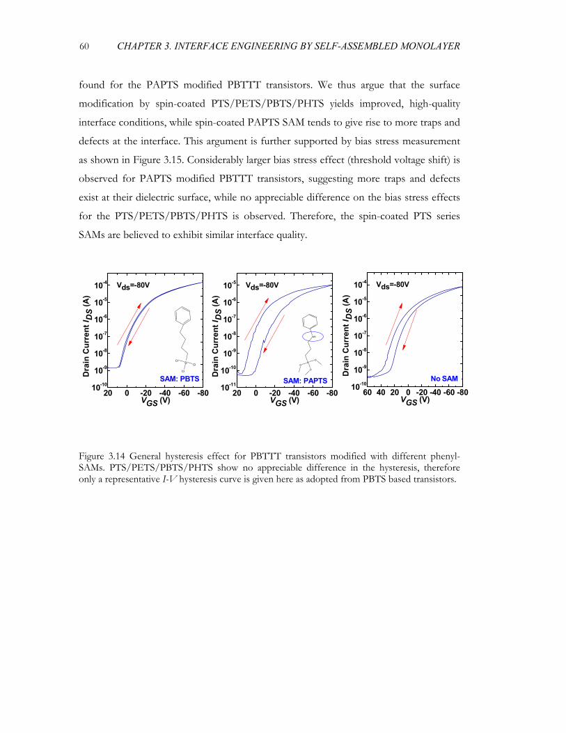
60 CHAPTER 3. INTERFACE ENGINEERING BY SELF-ASSEMBLED MONOLAYER
found for the PAPTS modified PBTTT transistors. We thus argue that the surface
modification by spin-coated PTS/PETS/PBTS/PHTS yields improved, high-quality
interface conditions, while spin-coated PAPTS SAM tends to give rise to more traps and
defects at the interface. This argument is further supported by bias stress measurement
as shown in Figure 3.15. Considerably larger bias stress effect (threshold voltage shift) is
observed for PAPTS modified PBTTT transistors, suggesting more traps and defects
exist at their dielectric surface, while no appreciable difference on the bias stress effects
for the PTS/PETS/PBTS/PHTS is observed. Therefore, the spin-coated PTS series
SAMs are believed to exhibit similar interface quality.
20 0 -20 -40 -60 -8010-10
10-9
10-8
10-7
10-6
10-5
10-4
VGS (V)
Dra
in C
urre
nt I D
S (A
)
SiCl
Cl
Cl
SAM: PBTS
Vds=-80V
20 0 -20 -40 -60 -8010-11
10-10
10-9
10-8
10-7
10-6
10-5
SiO
O
O
NH
VGS (V)
Dra
in C
urre
nt I D
S (A
)
SAM: PAPTS
Vds=-80V
60 40 20 0 -20 -40 -60 -8010-10
10-9
10-8
10-7
10-6
10-5
10-4
VGS (V)
Dra
in C
urre
nt I D
S (A
)
No SAM
Vds=-80V
Figure 3.14 General hysteresis effect for PBTTT transistors modified with different phenyl-SAMs. PTS/PETS/PBTS/PHTS show no appreciable difference in the hysteresis, therefore only a representative I-V hysteresis curve is given here as adopted from PBTS based transistors.
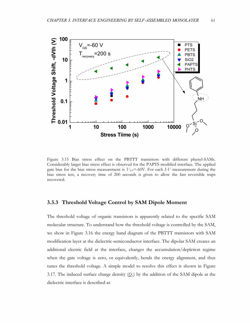
CHAPTER 3. INTERFACE ENGINEERING BY SELF-ASSEMBLED MONOLAYER 61
1 10 100 1000 100000.01
0.1
1
10
100
Thre
shol
d Vo
ltage
Shi
ft, -d
Vth
(V)
Stress Tiime (s)
PTS PETS PBTS SiO2 PAPTS PHTS
VGS=-60 VTrecovery=200 s
Si O
OO
NH
Figure 3.15 Bias stress effect on the PBTTT transistors with different phenyl-SAMs. Considerably larger bias stress effect is observed for the PAPTS modified interface. The applied gate bias for the bias stress measurement is VGS=-60V. For each I-V measurement during the bias stress test, a recovery time of 200 seconds is given to allow the fast reversible traps recovered.
3.3.3 Threshold Voltage Control by SAM Dipole Moment
The threshold voltage of organic transistors is apparently related to the specific SAM
molecular structure. To understand how the threshold voltage is controlled by the SAM,
we show in Figure 3.16 the energy band diagram of the PBTTT transistors with SAM
modification layer at the dielectric-semiconductor interface. The dipolar SAM creates an
additional electric field at the interface, changes the accumulation/depletion regime
when the gate voltage is zero, or equivalently, bends the energy alignment, and thus
tunes the threshold voltage. A simple model to resolve this effect is shown in Figure
3.17. The induced surface charge density (QS) by the addition of the SAM dipole at the
dielectric interface is described as
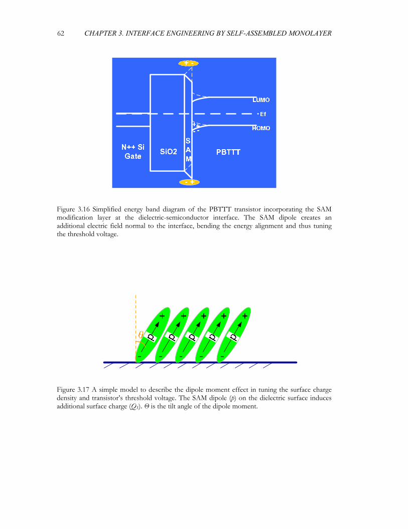
62 CHAPTER 3. INTERFACE ENGINEERING BY SELF-ASSEMBLED MONOLAYER
Figure 3.16 Simplified energy band diagram of the PBTTT transistor incorporating the SAM modification layer at the dielectric-semiconductor interface. The SAM dipole creates an additional electric field normal to the interface, bending the energy alignment and thus tuning the threshold voltage.
Figure 3.17 A simple model to describe the dipole moment effect in tuning the surface charge density and transistor’s threshold voltage. The SAM dipole (p) on the dielectric surface induces additional surface charge (QS). Θ is the tilt angle of the dipole moment.
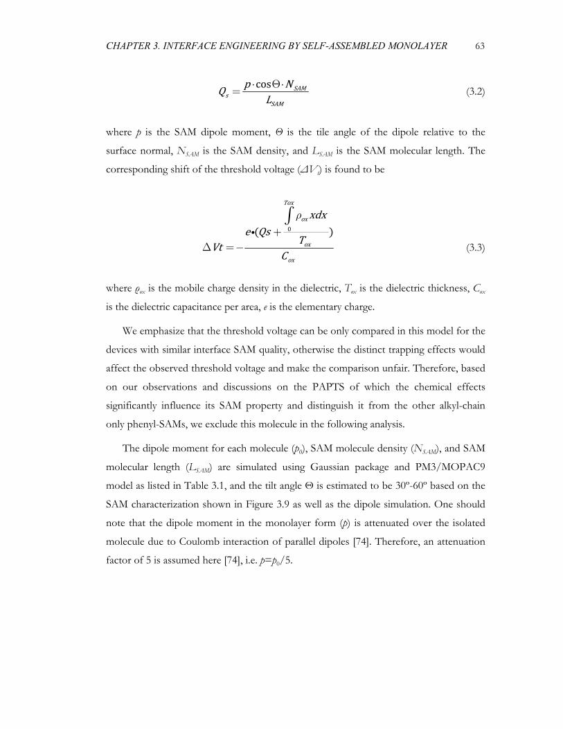
CHAPTER 3. INTERFACE ENGINEERING BY SELF-ASSEMBLED MONOLAYER 63
cos SAMs
SAM
p NQL
⋅ Θ⋅= (3.2)
where p is the SAM dipole moment, Θ is the tile angle of the dipole relative to the
surface normal, NSAM is the SAM density, and LSAM is the SAM molecular length. The
corresponding shift of the threshold voltage (ΔVt) is found to be
0
Tox
ox
ox
ox
xdxe Qs
TVtC
ρ+
Δ =−
∫i
(3.3)
where ρox is the mobile charge density in the dielectric, Tox is the dielectric thickness, Cox
is the dielectric capacitance per area, e is the elementary charge.
We emphasize that the threshold voltage can be only compared in this model for the
devices with similar interface SAM quality, otherwise the distinct trapping effects would
affect the observed threshold voltage and make the comparison unfair. Therefore, based
on our observations and discussions on the PAPTS of which the chemical effects
significantly influence its SAM property and distinguish it from the other alkyl-chain
only phenyl-SAMs, we exclude this molecule in the following analysis.
The dipole moment for each molecule (p0), SAM molecule density (NSAM), and SAM
molecular length (LSAM) are simulated using Gaussian package and PM3/MOPAC9
model as listed in Table 3.1, and the tilt angle Θ is estimated to be 30º-60º based on the
SAM characterization shown in Figure 3.9 as well as the dipole simulation. One should
note that the dipole moment in the monolayer form (p) is attenuated over the isolated
molecule due to Coulomb interaction of parallel dipoles [74]. Therefore, an attenuation
factor of 5 is assumed here [74], i.e. p=p0/5.
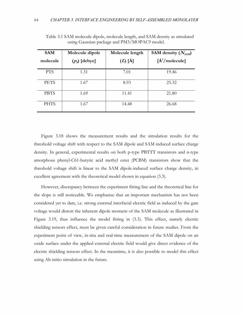
64 CHAPTER 3. INTERFACE ENGINEERING BY SELF-ASSEMBLED MONOLAYER
Table 3.1 SAM molecule dipole, molecule length, and SAM density as simulated using Gaussian package and PM3/MOPAC9 model.
SAM
molecule
Molecule dipole
(p0) [debye]
Molecule length
(L) [Å]
SAM density (NSAM)
[Å2/molecule]
PTS 1.31 7.01 19.46
PETS 1.67 8.93 25.32
PBTS 1.69 11.41 21.80
PHTS 1.67 14.48 26.68
Figure 3.18 shows the measurement results and the simulation results for the
threshold voltage shift with respect to the SAM dipole and SAM induced surface charge
density. In general, experimental results on both p-type PBTTT transistors and n-type
amorphous phenyl-C61-butyric acid methyl ester (PCBM) transistors show that the
threshold voltage shift is linear to the SAM dipole-induced surface charge density, in
excellent agreement with the theoretical model shown in equation (3.3).
However, discrepancy between the experiment fitting line and the theoretical line for
the slope is still noticeable. We emphasize that an important mechanism has not been
considered yet to date, i.e. strong external interfacial electric field as induced by the gate
voltage would distort the inherent dipole moment of the SAM molecule as illustrated in
Figure 3.19, thus influence the model fitting in (3.3). This effect, namely electric
shielding tensors effect, must be given careful consideration in future studies. From the
experiment point of view, in-situ and real-time measurement of the SAM dipole on an
oxide surface under the applied external electric field would give direct evidence of the
electric shielding tensors effect. In the meantime, it is also possible to model this effect
using Ab-initio simulation in the future.
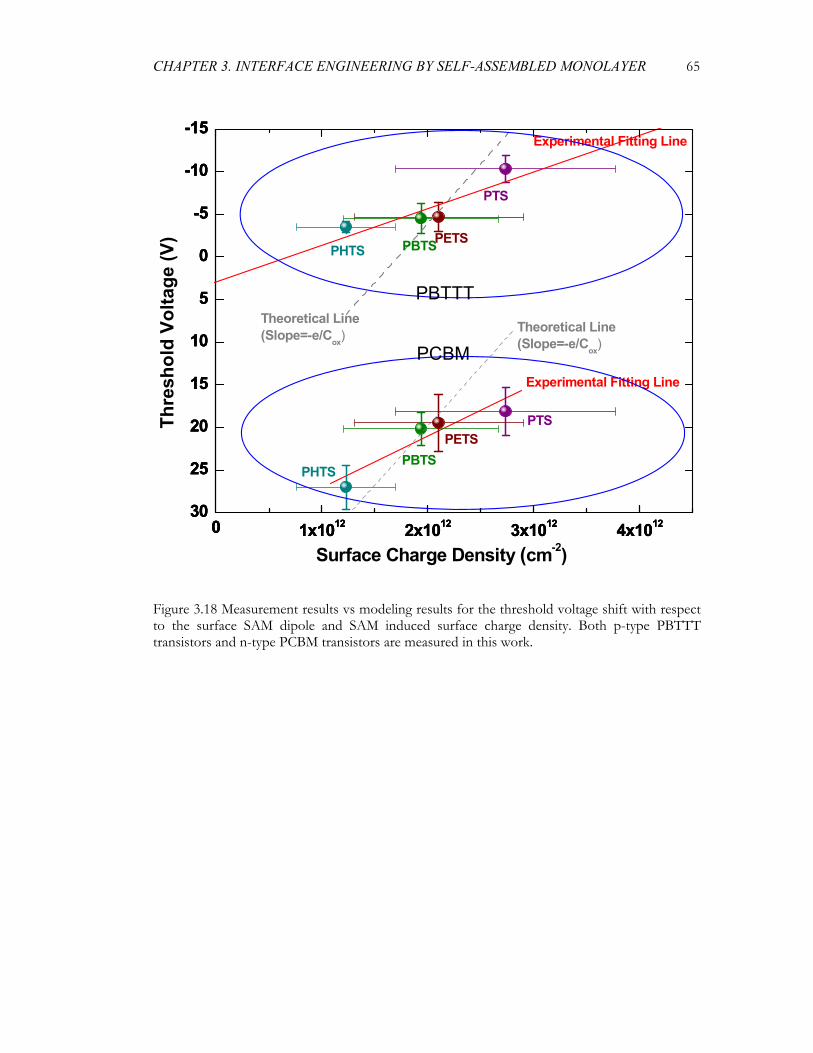
CHAPTER 3. INTERFACE ENGINEERING BY SELF-ASSEMBLED MONOLAYER 65
0 1x10¹² 2x10¹² 3x10¹² 4x101230
25
20
15
10
5
0
-5
-10
-15
0 1x10¹² 2x10¹² 3x10¹² 4x101230
25
20
15
10
5
0
-5
-10
-15
0 1x10¹² 2x10¹² 3x10¹² 4x101230
25
20
15
10
5
0
-5
-10
-15
PTSPETS
PBTSPHTS
Theoretical Line (Slope=-e/Cox)
Experimental Fitting Line
PTS
PETSPBTS
Experimental Fitting Line
Thre
shol
d Vo
ltage
(V)
Surface Charge Density (cm-2)
Theoretical Line (Slope=-e/Cox)
PHTS
PBTTT
PCBM
Figure 3.18 Measurement results vs modeling results for the threshold voltage shift with respect to the surface SAM dipole and SAM induced surface charge density. Both p-type PBTTT transistors and n-type PCBM transistors are measured in this work.
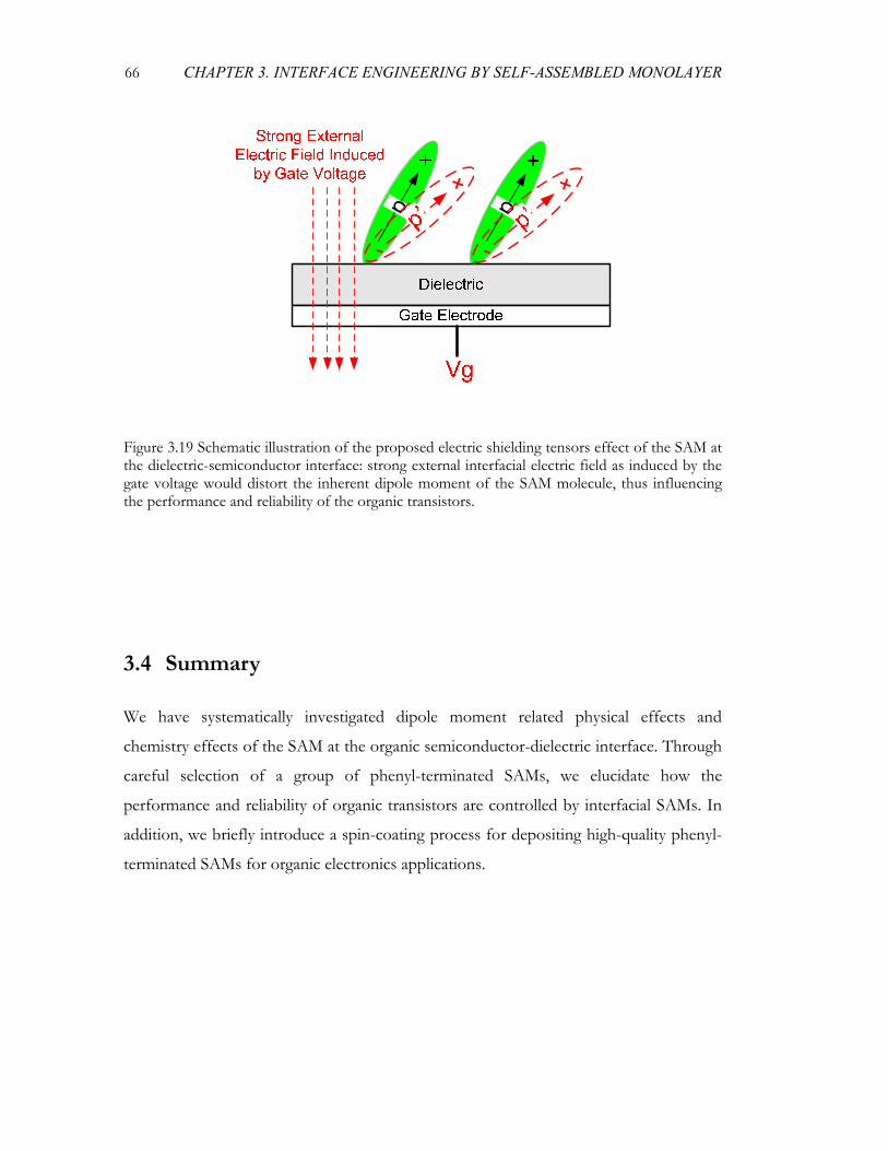
66 CHAPTER 3. INTERFACE ENGINEERING BY SELF-ASSEMBLED MONOLAYER
Figure 3.19 Schematic illustration of the proposed electric shielding tensors effect of the SAM at the dielectric-semiconductor interface: strong external interfacial electric field as induced by the gate voltage would distort the inherent dipole moment of the SAM molecule, thus influencing the performance and reliability of the organic transistors.
3.4 Summary
We have systematically investigated dipole moment related physical effects and
chemistry effects of the SAM at the organic semiconductor-dielectric interface. Through
careful selection of a group of phenyl-terminated SAMs, we elucidate how the
performance and reliability of organic transistors are controlled by interfacial SAMs. In
addition, we briefly introduce a spin-coating process for depositing high-quality phenyl-
terminated SAMs for organic electronics applications.
67
Chapter 4
Device Physics and Universal
Modeling of Organic Transistor
In physics, your solution should convince a reasonable person. In math, you have to convince a
person who's trying to make trouble. Ultimately, in physics, you're hoping to convince Nature.
And I've found Nature to be pretty reasonable.
- Frank Wilczek
So far we have presented the experimental demonstration of high-performance flexible
organic thin-film transistors based on solution process and systematically investigated
the electrical performance and reliability controlled by the semiconductor-dielectric
interfacial monolayer. In this chapter, we’ll study the device physics of organic
transistors with focus on charge injection effects at the metal-organic interface and
charge transport properties in the organic semiconductor film. A universal device model
capturing many of the physical effects observed for organic transistors will be
introduced [75].
68 CHAPTER 4. DEVICE PHYSICS AND MODELING OF ORGANIC TRANSISTOR
4.1 Background and Motivation
As an important figure of merit for transistors, the transition frequency, defined by
fT ∝ μFETV/2πL2, reflects circuit switching speed/bandwidth and strongly depends on
the extrinsic field-effect mobility (μFET)1 as well as the channel length (L). Therefore,
appropriate downscaling of the organic thin-film transistor, resembling that of
traditional silicon MOSFET which has been substantially benefited from the
sophisticated device scaling theories [1], is also crucial for the development of organic
electronic circuits and systems. Earlier works have explored organic transistors with
channel lengths from hundreds of micrometers down to sub-100 nm [76-84].
Experimental results show that the extrinsic field-effect mobility of these transistors is
channel-length variant, typically, with a lower value for sub-micrometer-channel devices.
As a consequence, the advantages originated from dimensional scaling to organic
circuits are severely compromised. Even for organic transistors with channel lengths
above micrometers, it is still not uncommon that the mobility decreases with shortening
of the channel length [81, 85-90]. Such channel-length dependence of the extrinsic
mobility has been suggested qualitatively to contact resistance effects; nevertheless,
analytical and quantitative studies remain in lack.
On the other hand, an inverse trend to the above mobility scaling behavior has been
reported for organic transistors more recently [15, 27, 43, 86, 91-92]. As briefly
mentioned in Chapter 2, for instance, we found an extrinsic field-effect mobility
decreasing with channel length for solution-processed, top-contact, polycrystalline
small-molecule organic TFTs [15, 43]. Hamadani et al. [91] and Verlaak et al. [92]
observed an higher effective mobility in the saturation regime for shorter channel
polythiophene-/pentacene-based TFTs and they attributed this to the electric field
dependence of charge transport. Gundlach et al. [27] and Smits et al. [86] found similar
mobility scaling behavior for contact-controlled polycrystalline acene-based TFTs and
quinquethiophene-based self-assembled-monolayer field-effect transistors (SAMFET),
1 In literature, it is also termed “apparent” or “effective” mobility, the value of which is extracted from the transfer curve in linear or saturation regime
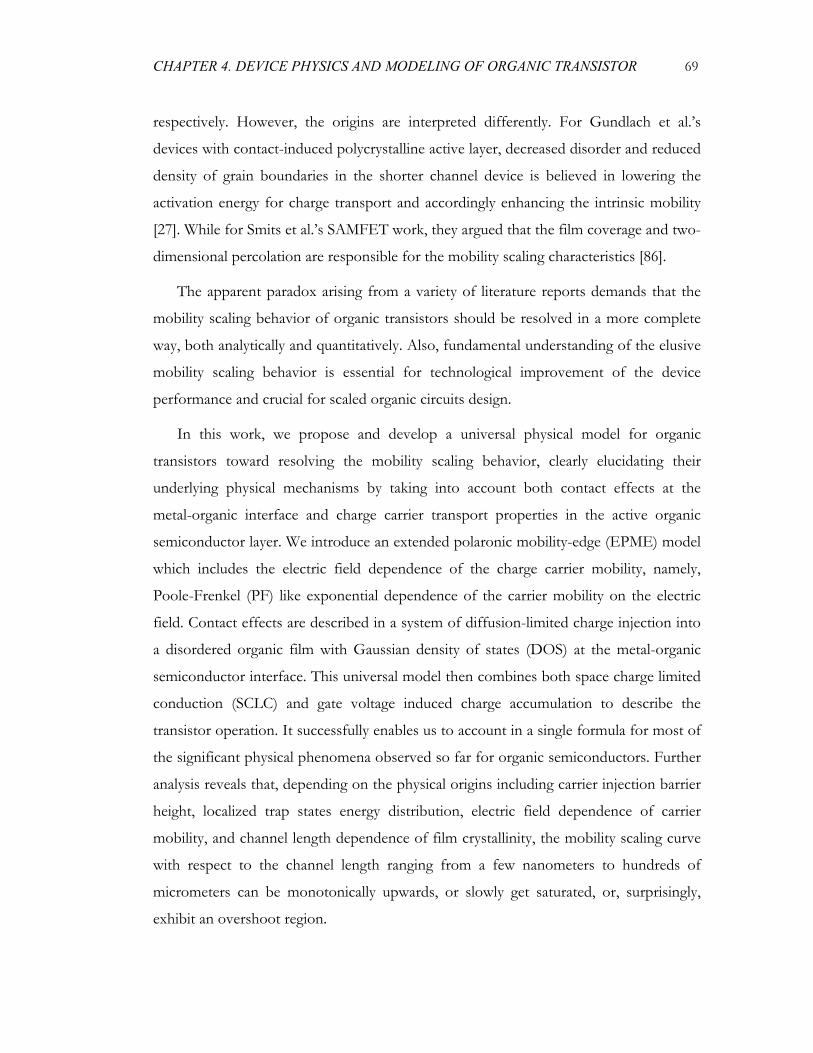
CHAPTER 4. DEVICE PHYSICS AND MODELING OF ORGANIC TRANSISTOR 69
respectively. However, the origins are interpreted differently. For Gundlach et al.’s
devices with contact-induced polycrystalline active layer, decreased disorder and reduced
density of grain boundaries in the shorter channel device is believed in lowering the
activation energy for charge transport and accordingly enhancing the intrinsic mobility
[27]. While for Smits et al.’s SAMFET work, they argued that the film coverage and two-
dimensional percolation are responsible for the mobility scaling characteristics [86].
The apparent paradox arising from a variety of literature reports demands that the
mobility scaling behavior of organic transistors should be resolved in a more complete
way, both analytically and quantitatively. Also, fundamental understanding of the elusive
mobility scaling behavior is essential for technological improvement of the device
performance and crucial for scaled organic circuits design.
In this work, we propose and develop a universal physical model for organic
transistors toward resolving the mobility scaling behavior, clearly elucidating their
underlying physical mechanisms by taking into account both contact effects at the
metal-organic interface and charge carrier transport properties in the active organic
semiconductor layer. We introduce an extended polaronic mobility-edge (EPME) model
which includes the electric field dependence of the charge carrier mobility, namely,
Poole-Frenkel (PF) like exponential dependence of the carrier mobility on the electric
field. Contact effects are described in a system of diffusion-limited charge injection into
a disordered organic film with Gaussian density of states (DOS) at the metal-organic
semiconductor interface. This universal model then combines both space charge limited
conduction (SCLC) and gate voltage induced charge accumulation to describe the
transistor operation. It successfully enables us to account in a single formula for most of
the significant physical phenomena observed so far for organic semiconductors. Further
analysis reveals that, depending on the physical origins including carrier injection barrier
height, localized trap states energy distribution, electric field dependence of carrier
mobility, and channel length dependence of film crystallinity, the mobility scaling curve
with respect to the channel length ranging from a few nanometers to hundreds of
micrometers can be monotonically upwards, or slowly get saturated, or, surprisingly,
exhibit an overshoot region.
70 CHAPTER 4. DEVICE PHYSICS AND MODELING OF ORGANIC TRANSISTOR
We stress that, beyond resolving the mobility scaling issue, our device model is also
versatile in explaining many other elusive physical phenomena for organic thin-film
transistors, such as the contact resistance effect and the surface potential profiles along
the channel which have been experimentally probed but yet poorly understood. Since
there is no commercially available device simulator dedicated for organic transistors
(unlike well-developed industry standard device simulator, e.g. Sentaurus, for traditional
silicon MOSFET), we implement the universal model into a 1-D device simulator for
organic TFTs. The simulation results of various electrical characteristics are in excellent
agreement with experimental observations.
4.2 Universal Modeling of Organic Transistors
There are a variety of structures available for standard organic TFTs [6], which can be
broadly categorized as bottom-contact and top-contact devices shown in Figure 1.2. A
compact model to describe the electrical characteristics of organic TFTs seemingly relies
on their particular structure [93-94], yet, the underlying physical mechanisms dominating
the device operation are consistent, and, are possible to describe in a generalized 1-D
manner as depicted in Figure 4.1.
Figure 4.1 A generalized 1-D representation of the physical process dominating the device operation for organic transistors.
CHAPTER 4. DEVICE PHYSICS AND MODELING OF ORGANIC TRANSISTOR 71
Charge carriers are first injected from the source electrode to the organic film
through the metal-organic semiconductor interface, then cross a transition region in the
vicinity of the source electrode before reaching the active channel layer. Eventually, the
charge carriers are extracted at the drain electrode through the metal-organic interface
immediately after traversing the other transition zone close to the drain. In bottom-
contact devices, the transition regions arise from enhanced structural disorder of the
organic semiconductor film deposited along the electrode edge as revealed by atomic
force microscopy (AFM) [95], and they tend to give rise to multifold effects, including:
• Charged traps enriched in the depletion zone screen out the gate voltage [96-97]
and lead to considerably lower free carrier concentration than that in the channel;
• Enhanced disorder and lower carrier concentration in the amorphous or
microcrystalline transition region reduce the effective carrier mobility;
• Disordered film structure induces inhomogeneities and energy level fluctuations at
the metal-organic semiconductor interface [97-104].
These effects must be carefully considered and taken into account for the device
modeling. Note that similar transition regions and relevant effects can be also identified
in top-contact devices as confirmed by both experimental observations [105] and
simulation results [93, 106-107]. The transition width (d(tr)), however, differs from in top-
contact and bottom-contact structures since the former is more heavily related to the
organic film thickness due to the fact that most charge carriers need to cross the entire
film to reach the interfacial channel. While for top-contact devices, metal evaporation
and organic film surface contamination are anticipated to cause conjugation break and
traps creation [105-106] in the neighborhood of the contacts, thus contribute to the
transition width.
Based on the above analysis, our universal device model incorporates contact effects
[88, 90, 93-97, 108-115] at the metal-organic interface as well as in its neighboring
transition region, and charge transport effects from the transition region to the active
channel. Since the contact resistance is normally found less pronounced at the drain for
charge extraction [112, 114], for simplicity, we only consider the lumped contact effects
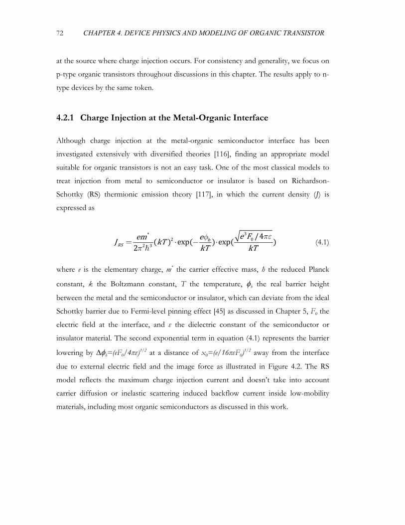
72 CHAPTER 4. DEVICE PHYSICS AND MODELING OF ORGANIC TRANSISTOR
at the source where charge injection occurs. For consistency and generality, we focus on
p-type organic transistors throughout discussions in this chapter. The results apply to n-
type devices by the same token.
4.2.1 Charge Injection at the Metal-Organic Interface
Although charge injection at the metal-organic semiconductor interface has been
investigated extensively with diversified theories [116], finding an appropriate model
suitable for organic transistors is not an easy task. One of the most classical models to
treat injection from metal to semiconductor or insulator is based on Richardson-
Schottky (RS) thermionic emission theory [117], in which the current density (J) is
expressed as
3*
022 3
/4exp exp
2b
RSe FeemJ kT
kT kTπεφ
π= ⋅ − ⋅ (4.1)
where e is the elementary charge, m* the carrier effective mass, ħ the reduced Planck
constant, k the Boltzmann constant, T the temperature, φb the real barrier height
between the metal and the semiconductor or insulator, which can deviate from the ideal
Schottky barrier due to Fermi-level pinning effect [45] as discussed in Chapter 5, F0 the
electric field at the interface, and ε the dielectric constant of the semiconductor or
insulator material. The second exponential term in equation (4.1) represents the barrier
lowering by ∆φb=(eF0/4πε)1/2 at a distance of x0=(e/16πεF0)1/2 away from the interface
due to external electric field and the image force as illustrated in Figure 4.2. The RS
model reflects the maximum charge injection current and doesn’t take into account
carrier diffusion or inelastic scattering induced backflow current inside low-mobility
materials, including most organic semiconductors as discussed in this work.
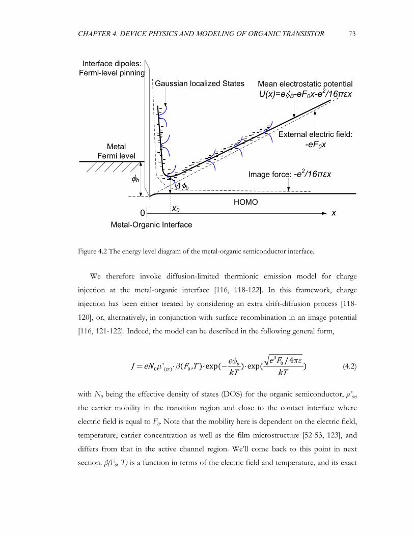
CHAPTER 4. DEVICE PHYSICS AND MODELING OF ORGANIC TRANSISTOR 73
Metal Fermi level
Metal-Organic Interface
b∆ b
External electric field:-eF0x
HOMO0 x
Image force: -e2/16πεx
Gaussian localized States Mean electrostatic potentialU(x)=e B-eF0x-e2/16πεx
x0
Interface dipoles:Fermi-level pinning
Figure 4.2 The energy level diagram of the metal-organic semiconductor interface.
We therefore invoke diffusion-limited thermionic emission model for charge
injection at the metal-organic interface [116, 118-122]. In this framework, charge
injection has been either treated by considering an extra drift-diffusion process [118-
120], or, alternatively, in conjunction with surface recombination in an image potential
[116, 121-122]. Indeed, the model can be described in the following general form,
3
00 0
/4' , exp expbtr
e FeJ eN F TkT kT
πεφμ β= ⋅ ⋅ − ⋅ (4.2)
with N0 being the effective density of states (DOS) for the organic semiconductor, μ’(tr)
the carrier mobility in the transition region and close to the contact interface where
electric field is equal to F0. Note that the mobility here is dependent on the electric field,
temperature, carrier concentration as well as the film microstructure [52-53, 123], and
differs from that in the active channel region. We’ll come back to this point in next
section. β(F0, T) is a function in terms of the electric field and temperature, and its exact
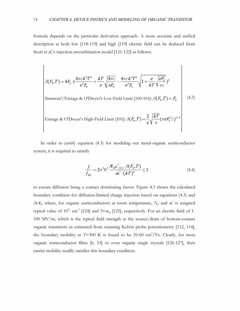
74 CHAPTER 4. DEVICE PHYSICS AND MODELING OF ORGANIC TRANSISTOR
formula depends on the particular derivation approach. A more accurate and unified
description at both low [118-119] and high [119] electric field can be deduced from
Scott et al.’s injection-recombination model [121-122] as follows:
2 2 2 220
0 0 3 30 0 0
0 0
3 1/40 0
4 4 4, 4 1
,
2,
eFk T kT k T eF T Fe F e eF e F kT
F T F
kTF T eFe
πε πε πεβπε
β
β π επ
⎧⎪⎪⎪⎪⎪⎪⎪ = ⋅ + − +
=⎨
=
Simmons'/Emtage & O'Dwyer's Low-Field Limit [100-101]:
Emtage & O'Dwyer's High-Field Limit [101]:
⎫⎪⎪⎪⎪⎪⎪⎪⎪ ⎪⎪ ⎪⎪ ⎪⎪ ⎪⎪ ⎪⎪ ⎪⎪ ⎪⎪ ⎪⎪ ⎪⎬⎪ ⎪⎪ ⎪⎪ ⎪⎪ ⎪⎪ ⎪⎪ ⎪⎪ ⎪⎪ ⎪⎪ ⎪⎪ ⎪⎪ ⎪⎪ ⎪⎪ ⎪⎪ ⎪⎪ ⎪⎪ ⎪⎩ ⎭
(4.3)
In order to justify equation (4.3) for modeling our metal-organic semiconductor
system, it is required to satisify
0 02 3* 2
' ,2 1tr
RS
N F TJJ m kT
μ βπ
⋅= ≤
⋅ (4.4)
to ensure diffusion being a contact dominating factor. Figure 4.3 shows the calculated
boundary condition for diffusion-limited charge injection based on equations (4.3) and
(4.4), where, for organic semiconductors at room temperature, N0 and m* is assigned
typical value of 1021 cm-3 [124] and 3×me0 [125], respectively. For an electric field of 1-
100 MV/m, which is the typical field strength at the source/drain of bottom-contact
organic transistors as estimated from scanning Kelvin probe potentiometry [112, 114],
the boundary mobility at T=300 K is found to be 10-60 cm2/Vs. Clearly, for most
organic semiconductor films [6, 53] or even organic single crystals [126-127], their
carrier mobility readily satisfies this boundary condition.
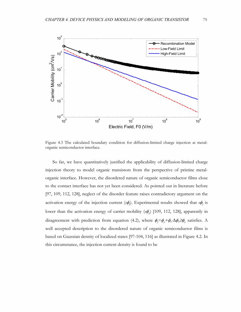
CHAPTER 4. DEVICE PHYSICS AND MODELING OF ORGANIC TRANSISTOR 75
105
106
107
108
109
10-2
10-1
100
101
102
103
Electric Field, F0 (V/m)
Car
rier M
obili
ty (c
m2 /V
s)
Recombination ModelLow-Field LimitHigh-Field Limit
Figure 4.3 The calculated boundary condition for diffusion-limited charge injection at metal-organic semiconductor interface.
So far, we have quantitatively justified the applicability of diffusion-limited charge
injection theory to model organic transistors from the perspective of pristine metal-
organic interface. However, the disordered nature of organic semiconductor films close
to the contact interface has not yet been considered. As pointed out in literature before
[97, 109, 112, 128], neglect of the disorder feature raises contradictory argument on the
activation energy of the injection current (eφJ). Experimental results showed that eφJ is
lower than the activation energy of carrier mobility (eφμ) [109, 112, 128], apparently in
disagreement with prediction from equation (4.2), where φJ=φμ+φb-∆φb≥φμ satisfies. A
well accepted description to the disordered nature of organic semiconductor films is
based on Gaussian density of localized states [97-104, 116] as illustrated in Figure 4.2. In
this circumstance, the injection current density is found to be
76 CHAPTER 4. DEVICE PHYSICS AND MODELING OF ORGANIC TRANSISTOR
30
0 0
2
2
320
0 0
/4' , exp exp
1 exp2 / 2
/4/2' , exp exp
tr
b
btr
e FeJ eN F TkT kT
e e de
e Fe kTeN F TkT kT
πεφμ β
φ φ φπσ σ
πεφ σμ β
+∞
−∞
⎡ ⎤⎢ ⎥= ⋅ ⋅ − ⋅ ⋅⎢ ⎥⎢ ⎥⎣ ⎦
⎡ ⎤− −⎢ ⎥⋅ ⎢ ⎥⎣ ⎦
−= ⋅ ⋅ − ⋅
∫
(4.5)
where σ is the Gaussian width of the localized states energy distribution. After taking
into account the Gaussian distribution of the localized states at the interface, we find the
activation energy of injection current is lowered by ∆σ=σ2/2kT≈50-200 meV for
T=300 K, σ=50-100 meV [97, 100-104, 109], thus being consistent with experimental
observations.
We emphasize that it is reasonable to treat charge injection at the metal-organic
interface separately from charge transport in the transition region beyond the interface
[97, 119]. Space charge effect is ignored in dealing with charge injection due to the fact
that the rapid variation of the electrostatic potential takes place within a short distance
from the electrode, typically x0=(e/16πεF0)1/2<10 Å, and the electric field F0 may be
regarded as being constant at the interface [119]. For charge transport in the transition
region with a typical width of d(tr)=20-200 nm [97, 109, 112], space charge effect
becomes pronounced since the field strength (F) in this region no longer satisfies the
condition of F>>2ned(tr)/ε~107 V/m, where n is the carrier concentration [119].
Therefore, we conclude that space charge limited conduction (SCLC) dominates the
charge transport in the organic transition region while diffusion limited charge injection
dominates at the metal-organic interface. As discussed in the following sections, they
naturally converge in the device operation through a self-consistent interfacial electric
field, F0. It has been suggested by Koehler et al. [97] recently that the commonly
observed yet poorly understood contact voltage/resistance for organic transistors may
originate from a combining effect of charge injection at the interface and SCLC in the
transition region. However, the feasibility of either mechanism for organic transistors is
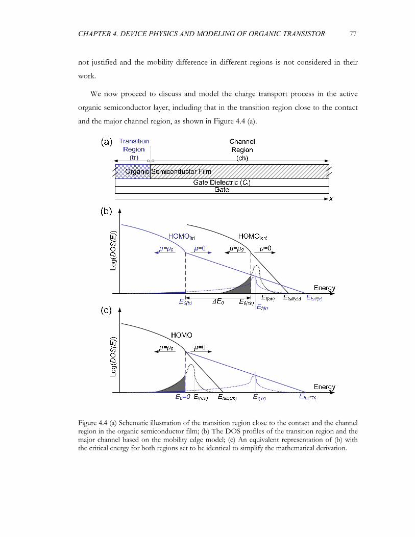
CHAPTER 4. DEVICE PHYSICS AND MODELING OF ORGANIC TRANSISTOR 77
not justified and the mobility difference in different regions is not considered in their
work.
We now proceed to discuss and model the charge transport process in the active
organic semiconductor layer, including that in the transition region close to the contact
and the major channel region, as shown in Figure 4.4 (a).
Figure 4.4 (a) Schematic illustration of the transition region close to the contact and the channel region in the organic semiconductor film; (b) The DOS profiles of the transition region and the major channel based on the mobility edge model; (c) An equivalent representation of (b) with the critical energy for both regions set to be identical to simplify the mathematical derivation.
78 CHAPTER 4. DEVICE PHYSICS AND MODELING OF ORGANIC TRANSISTOR
4.2.2 Charge Transport in the Active Layer: EPME Model
Here we discuss charge transport in the active semiconductor layer which is obviously
not a pure organic single crystal. Instead, it is an amorphous or polycrystalline organic
film coupled with disorders, traps and defects. These nonidealities give rise to a broad
distribution of Anderson localized states [129], and, accordingly, band only transport
description is unrealistic.
In general, there are two families of classical models available in dealing with charge
transport process in the disordered small-molecule or polymer films. One is based on
the hopping theory, including Miller-Abrahams’ fixed range hopping model [130] and
Mott’s variable range hopping (VRH) model [131], which calculate thermally activated
tunneling events between localized states. In this theoretical framework, carriers may
either hop to a nearest site with large activation energy or a distant site with low
activation energy. Vissenberg and Matters [132] have successfully applied this concept in
conjunction with a percolation criterion for the film conduction to the carrier mobility
model for amorphous organic TFTs. The other one is based on the mobility edge (ME)
concept [131, 133-134] as illustrated in Figure 4.4, or, equivalently, multiple trapping and
release (MTR) concept [135-136], which defines a critical energy (E0, the “mobility
edge”) separating immobile localized states (μ=0) with a DOS tail in the forbidden
bandgap from the extended band of mobile states (μ=μ0). Trapped carriers become
mobile by thermal excitation into the delocalized band and thereby contribute to the
conduction. This model has been successfully applied to study semicrystalline polymer
transistors by Salleo et al. [133] and later refined by Chang et al. [137] by incorporating
the polaronic effect.
For the work presented here, we choose the ME theoretical framework since
hopping transport theory such as the VRH model doesn’t take into account the nature
of supramolecular ordering and mesoscale microstructure in the semi- or poly-crystalline
organic semiconductor films. Also, ME model has been shown from studies of the
microstructure effect and polaronic effect on the carrier mobility that it provides an
improved fitting to the experimental data over VRH based model [133, 137]. It should
CHAPTER 4. DEVICE PHYSICS AND MODELING OF ORGANIC TRANSISTOR 79
be noted that, however, previous ME models adopted for organic transistors haven’t yet
considered the electric field effect on the mobility. Since the electric filed dependence of
the mobility becomes pronounced at low temperature or high field, which is the
situation typically found in the transition region as discussed in last section, we therefore
first develop an extended polaronic mobility edge (EPME) model here by taking into
account the field dependence of the carrier mobility. This EPME model for charge
transport is then integrated into our universal device model for describing the organic
transistor operation.
As shown in Figure 4.4 (b), the DOS profiles of the organic semiconductor films are
represented by a delocalization band with an exponential tail of donor-like localized
states decaying into the bandgap [133]. The exponential tail here is an approximation of
the Gaussian profile generally accepted for disordered organic semiconductors. First
principle calculations on the electronic structure of polycrystalline polymers [138] have
explicitly shown that the carrier delocalization in ordered lamellas increases the
bandwidths for both the highest occupied molecular orbital (HOMO) and the lowest
unoccupied molecular orbital (LUMO), consequently, giving rise to a bandgap reduction.
Therefore, considering the different disorder levels in the transition region and in the
channel region as discussed at the beginning of Section 4.2, we propose that the critical
energy defining the mobility edge (E0) is shifted by ∆E0=E0(Ch)-E0(Tr), roughly 0.2-0.4 eV,
between these two regions. The DOS profiles shown in Figure 4.4 (b) are described as
0 0
0 0
1 sgnexp2
1 sgn12
tail
tail tail
tail
tail c
N E E E EDOS EE E
N E E E EE E
− − + −= ⋅ ⋅Δ Δ
− + −+ ⋅ − ⋅Δ
(4.6)
where sgn(x) is the sign function, Ec is a parameter to tailor the DOS profile for the band,
Ntail is the concentration of tail states, ∆Etail=Etail-E0 is the tail width of the localized
states. The DOS for the delocalization band is simply represented with a form for 3-D
free hole gas. The above parameters accompanied by a footnote, “tr” or “ch”, in Figure
80 CHAPTER 4. DEVICE PHYSICS AND MODELING OF ORGANIC TRANSISTOR
4.4 (b), denote those for the transition region or the channel region, respectively. One
should note that the tail states concentration and band mobility (μ=μ0) are assumed
identical for both regions since the major distinction induced by structural modifications
is the localized tail width [133].
When a gate voltage (VGS) applies, charges tend to accumulate along the organic
semiconductor-dielectric interface. The total charge density, including that of immobile
localized trap states and mobile free carriers, can be approximated as
, i GS ontot GS
C V VN V Th−= (4.7)
where Ci is the dielectric capacitance per area, Von is the turn-on voltage, or, equivalently,
the flat band threshold voltage when charge start to accumulate, which ideally should be
around 0 V [36], h is the first-order approximation of the charge layer thickness (~1 nm)
at the dielectric-semiconductor interface.
On the other hand, Figure 4.4 indicates that the total charge density, Ntot(VGS, T),
and the mobile carrier concentration, Nmob(VGS, T), are represented as follows:
, 1tot GSN V T DOS E F E dE+∞
−∞= ⋅ −∫ (4.8)
0
, 1E
mob GSN V T DOS E F E dE−∞
= ⋅ −∫ (4.9)
where
/1
1 fE E kTF Ee −=+
(4.10)
is the Fermi-Dirac distribution. Combine equations (4.6)-(4.10), we can readily find the
solution to Fermi energy, Ef., and the results apply to both the transition region (“tr”)
and the channel region (“ch”). Figure 4.5 shows the calculated relationship between the
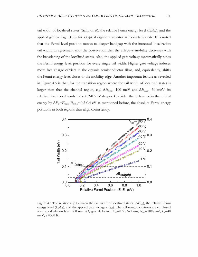
CHAPTER 4. DEVICE PHYSICS AND MODELING OF ORGANIC TRANSISTOR 81
tail width of localized states (∆Etail or σ), the relative Fermi energy level (Ef-E0), and the
applied gate voltage (VGS) for a typical organic transistor at room temperate. It is noted
that the Fermi level position moves to deeper bandgap with the increased localization
tail width, in agreement with the observation that the effective mobility decreases with
the broadening of the localized states. Also, the applied gate voltage systematically tunes
the Fermi energy level position for every single tail width. Higher gate voltage induces
more free charge carriers in the organic semiconductor films, and, equivalently, shifts
the Fermi energy level closer to the mobility edge. Another important feature as revealed
in Figure 4.5 is that, for the transition region where the tail width of localized states is
larger than that the channel region, e.g. ∆Etail(tr)=100 meV and ∆Etail(tr)=30 meV, its
relative Fermi level tends to be 0.2-0.5 eV deeper. Consider the difference in the critical
energy by ∆E0=E0(Ch)-E0(Tr),~0.2-0.4 eV as mentioned before, the absolute Fermi energy
positions in both regions thus align consistently.
0.0 0.2 0.4 0.6 0.8 1.00.0
0.1
0.2
0.3
0.4
ΔEtail(ch)
ΔEtail(tr)-1 V
-10 V-20 V
-40 V-60 V-80 V
Tail
Wid
th (e
V)
Relative Fermi Position, Ef-E0 (eV)
VGS=-100 V
0.0
0.1
0.2
0.3
0.4
Figure 4.5 The relationship between the tail width of localized states (∆Etail), the relative Fermi energy level (Ef-E0), and the applied gate voltage (VGS). The following conditions are employed for the calculation here: 300 nm SiO2 gate dielectric, Von=0 V, h=1 nm, Ntail=1021/cm3, Ec=40 meV, T=300 K.
82 CHAPTER 4. DEVICE PHYSICS AND MODELING OF ORGANIC TRANSISTOR
Without incorporating polaronic effect, the overall effective carrier mobility, μeff, is
simply defined as μeff=μ0×(Nmob/Ntot) [133]. In reality, strong electron-phonon coupling
existing in the conjugated organic semiconductor molecules or polymers leads to
polaron formation and thus contributes to the temperature activation of the carrier
mobility. A refined description of the effective mobility has been suggested [137] as
0,, exp,
mob GS aeff GS
tot GS
N V T EV TN V T kT
μ μ= ⋅ ⋅ − (4.11)
where the polaronic effect is represented by an extra exponential term, based on the
assumption that the mobility beyond the mobility edge is thermally activated with a
polaron activation energy of Ea.
Another important factor in determining the carrier mobility behavior is the electric
field dependence, which has been an active research subject for disordered organic
materials. It is now well recognized that this dependence strongly relies on the
temperature and field range as well as the film’s structural properties, such as energetic
or positional disorder levels [139-146]. A routine finding on organic semiconductors,
from both Monte Carlo simulations [139-142] and experiments [143-146], is that within
an intermediate field range, typically 104-106 V/cm, the field-dependent mobility exhibits
the Poole-Frenkel like behavior and can be described in a general form as
1exp n FT
μ γ∝ ⋅ (4.12)
where γ(1/Tn) is an empirical parameter relying on temperature (T), n=1-2 [139, 141-
146]. Note that the lateral field strengths for the transition region and the channel region
shown in Figure 4.4 (a) can be considerably different. Therefore, a rough estimation of
the average field by F=VDS/L (L is the channel length) as frequently seen in literature is
not necessarily correct. We estimate the field strengths here from the scanning probe
potentiometry profiles [112, 114] and find that the field dependence as described in
(4.12) is appropriate in both regions. However, it should be stressed that, due to their
CHAPTER 4. DEVICE PHYSICS AND MODELING OF ORGANIC TRANSISTOR 83
appreciable difference in the film microstructure and thus energetic/spatial disorder,
γ(1/Tn) for the transition region is expected larger than the less disordered channel
region: γ(tr)(1/Tn)>γ(ch)(1/Tn). This can be inferred from Bässler’s formula [139],
2 20
1n C
T kTσγ = ⋅ −∑ (4.13)
where σ is the energetic width of the Gaussian DOS, ∑ represents the off-diagonal
(spatial) disorder. For disordered organic materials, γ(1/Tn) is normally 0.001-0.005
cm1/2V-1/2 at room temperature. With the increasingly ordered structure (or smaller σ)
and higher temperature, γ(1/Tn) eventually vanishes or even turns negative [140, 143].
The extended polaronic mobility edge (EPME) model proposed in this work
incorporates the effective mobility derived in (4.11) as the prefactor for the field-
dependent mobility described in (4.12). The carrier concentration, temperature, and
electric field-dependent effective mobility is expressed collectively as below:
0, 1, , exp exp,
mob GS aeff GS n
tot GS
N V T EV T F FN V T kT T
μ μ γ= ⋅ ⋅ − ⋅ ⋅ (4.14)
Equation (4.14) is a general form adequate for both the transition region and the
channel region. Here we assume the EPME effective mobility derived for charge carriers
located at the dielectric-semiconductor interface applies to the entire film thickness. This
approximation is judged from the nature of mobility edge model which inherently
relates the film microstructure to the effective mobility. For clarity, we reiterated the
mobility in both regions as follows:
0
, 1, , exp exp,
mob tr GS atr GS tr n
tot GS
N V T EV T F FN V T kT T
μ μ γ= ⋅ ⋅ − ⋅ ⋅ (4.15)
84 CHAPTER 4. DEVICE PHYSICS AND MODELING OF ORGANIC TRANSISTOR
0
, 1, , exp exp,
mob ch GS ach GS ch n
tot GS
N V T EV T F FN V T kT T
μ μ γ= ⋅ ⋅ − ⋅ ⋅ (4.16)
We emphasize that, in circumstances such as in contact-induced polycrystalline
organic thin film transistors [27], solution-shearing processed polycrystalline organic
transistors [15, 38, 43], etc., the overall film crystallinity is correlated to the channel
length. The channel length dependent crystallinity will thus affect the μ(ch) in (4.16) by an
additional function of channel length. We’ll return to this point when discussing the
mobility scaling behavior in Section 4.3.3.
4.2.3 Unified Model for Transistor Operations
Based on the discussion and analysis in Sections 4.2.1 and 4.2.2, we are now able to
combine all of the effects to describe the transistor operation. Since SCLC dominates in
some local regions, it is necessary to include in the overall drain current (IDS) both the
SCLC current arising from the drain-source voltage (VDS) and the charge accumulation
current arising from the gate-source voltage (VGS). Accordingly, we have
DS SCLC tr accumulation tr SCLC ch accumulation chI I I I I= + = + (4.17)
For SCLC component with negligible diffusion current, it follows Gauss’s law
eF ρε
∇⋅ = (4.18)
and the current transport equation
, , , , xSCLC SCLC SCLC x GS x x GS x
dFI J A WHe F V T F WHF V T Fdx
ρ μ μ ε= ⋅ ≅ = ⋅ ⋅ ⋅ (4.19)
CHAPTER 4. DEVICE PHYSICS AND MODELING OF ORGANIC TRANSISTOR 85
where ρ is the charge carrier density, x denotes the channel direction from source (x=0)
to drain (x=L) as shown in Figure 4.4 (a), ASCLC is the effective cross sectional area for
the SCLC current. In a first-order approximation, ASCLC =W×H, where W is the
transistor’s channel width, H is the organic semiconductor film thickness.
For charge accumulation induced by the gate voltage at the dielectric-semiconductor
interface, it contributes to the drain current at position x by
, ,accumulation GS x x i GS on xI V T F F C W V V Vμ= ⋅ ⋅ ⋅ ⋅ − − (4.20)
where Vx is the electrical potential at position x resulted from the drain-source voltage,
and it relates to the electric field (Fx) by
x xF V=−∇⋅ (4.21)
and
0 0
L L
x x DSF dx V dx V= −∇⋅ =−∫ ∫ (4.22)
Plug equations (4.15), (4.16), and (4.19)-(4.22) into equation (4.17), we have
0
'0
, 1exp exp,
'
mob GS aDS x xn
tot GS
xx
i GS on x
N V T EI WF FN V T kT T
dFH C V V F dxdx
μ γ
ε
= ⋅ ⋅ − ⋅ ⋅
× ⋅ ⋅ + ⋅ − +∫
(4.23)
Integration of equation (4.23) from x=0 to x=L on both sides yields the drain
current equation for the transistor as follows:
86 CHAPTER 4. DEVICE PHYSICS AND MODELING OF ORGANIC TRANSISTOR
0 0
'0
,1exp exp,
'
La mob GS
DS x xntot GS
xx
i GS on x
E N V TWI F FL kT T N V T
dFH C V V F dx dxdx
μ γ
ε
⎧⎪⎪= − ⋅ ⋅ ⋅⎨⎪⎪⎩
⋅ ⋅ ⋅ + ⋅ − +
∫
∫
(4.24)
Alternatively, equation (4.24) can be formulized with the transition region and the
channel region described by separate terms,
0 0
'0
0
,1exp exp,
'
1exp exp
trd mob tr GSaDS x tr xn
tot GS
xx
i GS on x
ax ch
N V TEWI F FL kT T N V T
dFH C V V F dx dxdx
EW FL kT T
μ γ
ε
μ γ
⎧⎪⎪= − ⋅ ⋅ ⋅⎨⎪⎪⎩
⋅ ⋅ ⋅ + ⋅ − +
+ − ⋅ ⋅
∫
∫
'0
,,
'
tr
L mob ch GSxnd tot GS
xx
i GS on x
N V TF
N V T
dFH C V V F dx dxdx
ε
⎧⎪⎪ ⋅⎨⎪⎪⎩
⋅ ⋅ ⋅ + ⋅ − +
∫
∫
(4.25)
where d(tr) is the width of the transition region, typically 20-200 nm.
Equation (4.23)-(4.25) are the derived current equation for organic transistors based
on our universal model incorporating both the charge injection effects and charge
transport properties. The model is essentially physics-oriented since each variable
involved has real and particular physical meanings. This model successfully enables us to
account in a single formula for most of the significant physical phenomena observed so
far for organic semiconductor films and their based transistors.
In order to solve the above differential equations to fully simulate the transistor’s
behavior, it is necessary to obtain the boundary conditions. Therefore, we invoke the
injection current density at the source contact, JSD, as given by equation (4.5) in Section
4.2.1. Substitute (4.15) for the mobility μ(tr) in (4.5), we obtain:
CHAPTER 4. DEVICE PHYSICS AND MODELING OF ORGANIC TRANSISTOR 87
3
0 0 0
2
0
/41exp exp
' /2, exp
aSD tr n
mob tr b
tot tr
eEJ eN FkT T kT
N e kTF TN kT
πεμ γ
φ σβ
= − ⋅ + ⋅
−⋅ ⋅ ⋅ −
(4.26)
Note that we distinguish μ’(tr) in equation (4.5) and μ(tr) in (4.15) by assuming that the
carrier mobility for charge injection at the metal-organic interface, i.e. μ’(tr) in (4.5), is
correlated to the film disorder or localized states tail width by N’mob(tr)/Ntot(tr)∝exp(-σ/kT),
and, is independent of the applied gate voltage. While for the charge transport mobility
in the film, i.e. μ(tr) in (4.15), it is apparently gate voltage dependent since Nmob(tr)/Ntot(tr) is
defined by equations (4.7)-(4.10).
The charge injection current equation (4.26) provides the following boundary
conditions for the transistor’s ordinary differential current equation (4.23),
DS SD inj SDI J A J WHα= ⋅ = ⋅ (4.27)
0 ' 00' 0
x
x xV F dx == − =∫ (4.28)
0 0x xF F == (4.29)
where Ainj is the effective injection area, α is a prefactor determined by the transistor
geometry. In addition, to resolve the full transistor behavior, another similar boundary
condition for F(x=d(tr)) and V(x= d(tr)) should also be employed at the transition and
channel region connection position, x=d(tr).
So far, we have analytically derived the universal device model by incorporating both
charge injection effects and charge transport properties for organic thin-film transistors.
This model has been implemented in C/Mathematica programs to render a full 1-D
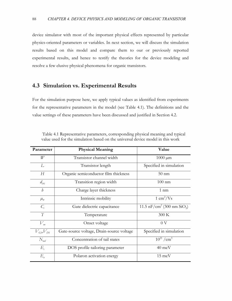
88 CHAPTER 4. DEVICE PHYSICS AND MODELING OF ORGANIC TRANSISTOR
device simulator with most of the important physical effects represented by particular
physics-oriented parameters or variables. In next section, we will discuss the simulation
results based on this model and compare them to our or previously reported
experimental results, and hence to testify the theories for the device modeling and
resolve a few elusive physical phenomena for organic transistors.
4.3 Simulation vs. Experimental Results
For the simulation purpose here, we apply typical values as identified from experiments
for the representative parameters in the model (see Table 4.1). The definitions and the
value settings of these parameters have been discussed and justified in Section 4.2.
Table 4.1 Representative parameters, corresponding physical meaning and typical value used for the simulation based on the universal device model in this work
Parameter Physical Meaning Value
W Transistor channel width 1000 µm
L Transistor length Specified in simulation
H Organic semiconductor film thickness 50 nm
d(tr) Transition region width 100 nm
h Charge layer thickness 1 nm
µ0 Intrinsic mobility 1 cm2/Vs
Ci Gate dielectric capacitance 11.5 nF/cm2 (300 nm SiO2)
T Temperature 300 K
Von Onset voltage 0 V
VGS,VDS Gate-source voltage, Drain-source voltage Specified in simulation
Ntail Concentration of tail states 1021 /cm3
Ec DOS profile tailoring parameter 40 meV
Ea Polaron activation energy 15 meV
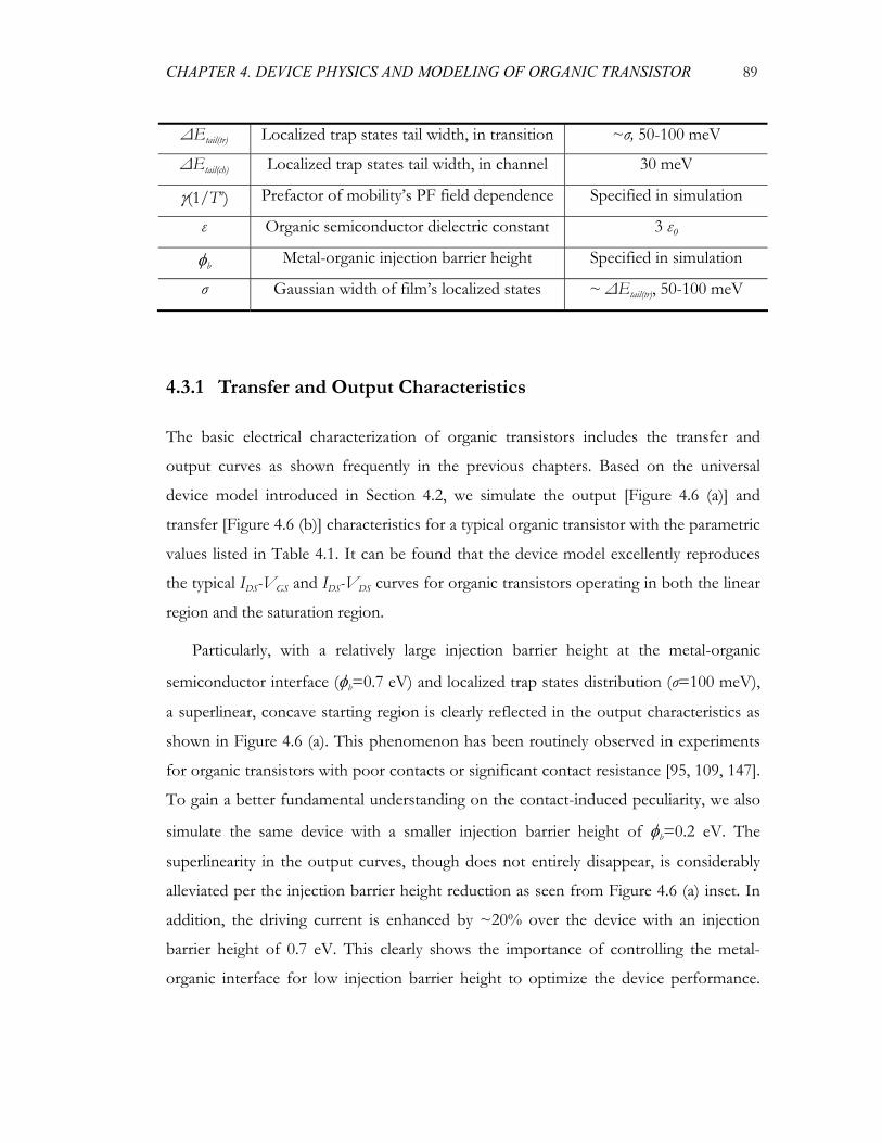
CHAPTER 4. DEVICE PHYSICS AND MODELING OF ORGANIC TRANSISTOR 89
ΔEtail(tr) Localized trap states tail width, in transition ~σ, 50-100 meV
ΔEtail(ch) Localized trap states tail width, in channel 30 meV
γ(1/Tn) Prefactor of mobility’s PF field dependence Specified in simulation
ε Organic semiconductor dielectric constant 3 ε0
φb Metal-organic injection barrier height Specified in simulation
σ Gaussian width of film’s localized states ~ ΔEtail(tr), 50-100 meV
4.3.1 Transfer and Output Characteristics
The basic electrical characterization of organic transistors includes the transfer and
output curves as shown frequently in the previous chapters. Based on the universal
device model introduced in Section 4.2, we simulate the output [Figure 4.6 (a)] and
transfer [Figure 4.6 (b)] characteristics for a typical organic transistor with the parametric
values listed in Table 4.1. It can be found that the device model excellently reproduces
the typical IDS-VGS and IDS-VDS curves for organic transistors operating in both the linear
region and the saturation region.
Particularly, with a relatively large injection barrier height at the metal-organic
semiconductor interface (φb=0.7 eV) and localized trap states distribution (σ=100 meV),
a superlinear, concave starting region is clearly reflected in the output characteristics as
shown in Figure 4.6 (a). This phenomenon has been routinely observed in experiments
for organic transistors with poor contacts or significant contact resistance [95, 109, 147].
To gain a better fundamental understanding on the contact-induced peculiarity, we also
simulate the same device with a smaller injection barrier height of φb=0.2 eV. The
superlinearity in the output curves, though does not entirely disappear, is considerably
alleviated per the injection barrier height reduction as seen from Figure 4.6 (a) inset. In
addition, the driving current is enhanced by ~20% over the device with an injection
barrier height of 0.7 eV. This clearly shows the importance of controlling the metal-
organic interface for low injection barrier height to optimize the device performance.
90 CHAPTER 4. DEVICE PHYSICS AND MODELING OF ORGANIC TRANSISTOR
The residual superlinearity for even low injection barrier height can be attributed to the
other factor, localized trap states distribution width (σ), as discussed in next section.
Compare the above simulation results to our 4T-TMS SPOFET performance as
presented in Chapter 2, we reaffirm the 4T-TMS SPOFET possesses favorable contacts
at the source/drain with a low contact injection barrier height and a narrow localized
trap states distribution in the organic film.
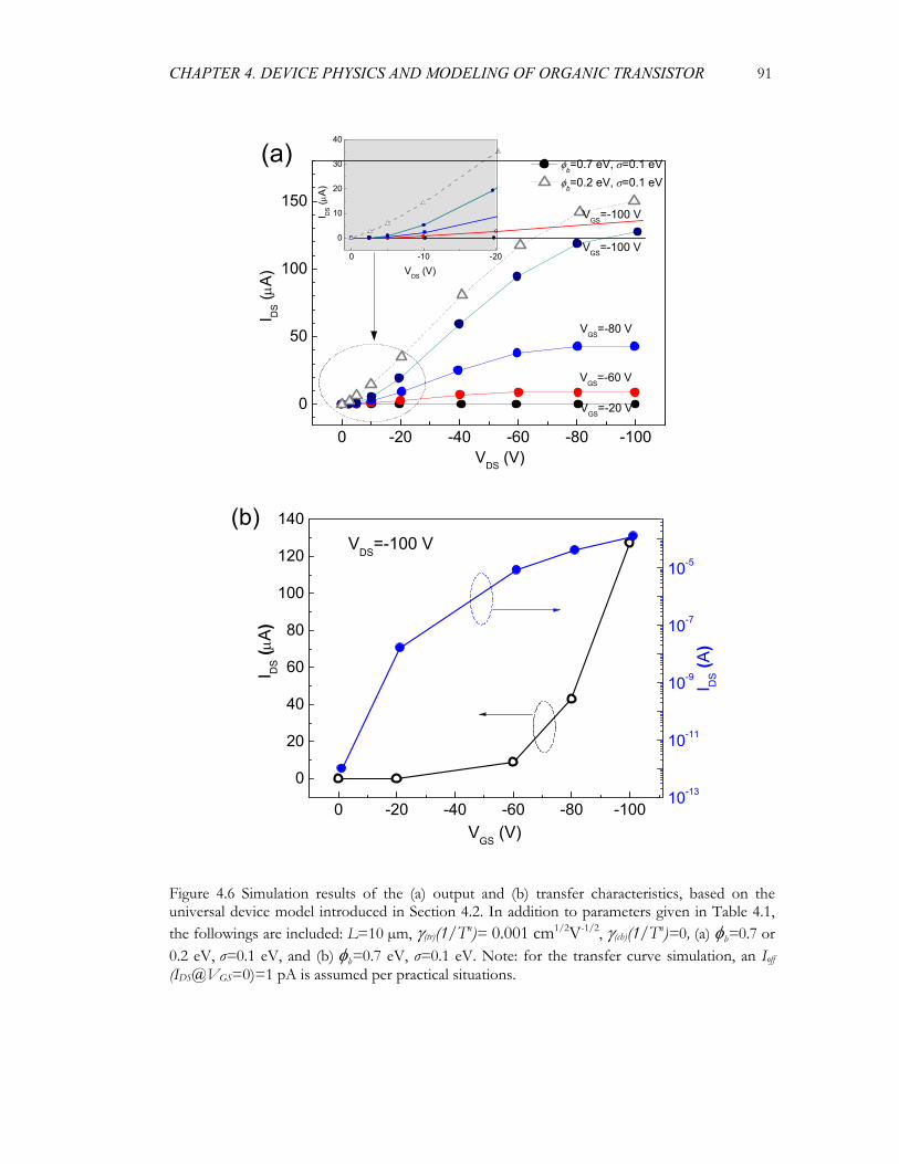
CHAPTER 4. DEVICE PHYSICS AND MODELING OF ORGANIC TRANSISTOR 91
0 -20 -40 -60 -80 -100
0
50
100
150
VGS=-20 V
VGS=-60 V
VGS=-80 V
VGS=-100 V
I DS (μ
A)
VDS (V)
φb=0.7 eV, σ=0.1 eV
φb=0.2 eV, σ=0.1 eV
VGS=-100 V
0 -10 -20
0
10
20
30
40
I DS (μ
A)
VDS
(V)
(a)
0 -20 -40 -60 -80 -100
0
20
40
60
80
100
120
140
VGS (V)
I DS (μ
A)
10-13
10-11
10-9
10-7
10-5
(b)
I DS (A
)
VDS=-100 V
Figure 4.6 Simulation results of the (a) output and (b) transfer characteristics, based on the universal device model introduced in Section 4.2. In addition to parameters given in Table 4.1, the followings are included: L=10 µm, γ(tr)(1/Tn)= 0.001 cm1/2V-1/2, γ(ch)(1/Tn)=0, (a) φb=0.7 or 0.2 eV, σ=0.1 eV, and (b) φb=0.7 eV, σ=0.1 eV. Note: for the transfer curve simulation, an Ioff
(IDS@VGS=0)=1 pA is assumed per practical situations.
92 CHAPTER 4. DEVICE PHYSICS AND MODELING OF ORGANIC TRANSISTOR
4.3.2 Surface Potential Profile and Contact Resistance
Surface potential profile along the dielectric-semiconductor interface has been well
studied and understood in traditional silicon MOSFETs [117]. It was until recently that
this topic was recognized to be critical in studying organic thin-film transistors. In fact,
the surface potential profile contains ample information on the transistor operation
status and the contact effects. A few early works have probed this potential profile for
organic transistors using high-resolution conductive probe atomic force microscopy
(AFM) [114], electrostatic force microscopy (EFM) [148], or scanning Kelvin probe
microscopy (SKPM) [112, 149], thus providing a foundation for justifying the electric
field distribution and estimating the contact resistance. However, the fundamental
physics and mechanisms responsible for these experimental observations are still poorly
understood.
Based on our universal model which takes into account both the charge injection
effects at the metal-organic interface and charge transport properties in the active film
layer, we are able to simulate the surface potential profile for the organic thin-film
transistors [see Figure 4.7 (a)]. Devices operating from linear regime (-VGS>-(VDS+VTH))
to saturation regime ((-VGS<-(VDS+VTH))) are explicitly revealed by the surface potential
profile change upon increase of the applied drain voltage. For –VDS>80 V, the channel
area close to the drain is gradually getting to depletion mode for saturation operation.
The channel regions which are in accumulation mode show a seemingly quasi-linear
potential profile and only consume little voltage drop along the channel, in distinct
contrast to the transition regions where a significant voltage drop occurs in the case of
φb=0.7 eV and σ=100 meV. This dramatic voltage consumption in a short distance close
to the source, i.e. the transition region as depicted in Figure 4.4 (a), contributes to the
extrinsically large contact resistance as regularly found in devices with poor contacts. For
direct comparison, Figure 4.7 (b) invokes a representative surface potential profile of the
P3HT-polymer transistor as recorded in experiments by noncontact potentiometry using
scanning Kelvin probe microscope by Bürgi et al. [112]. It can be found that the
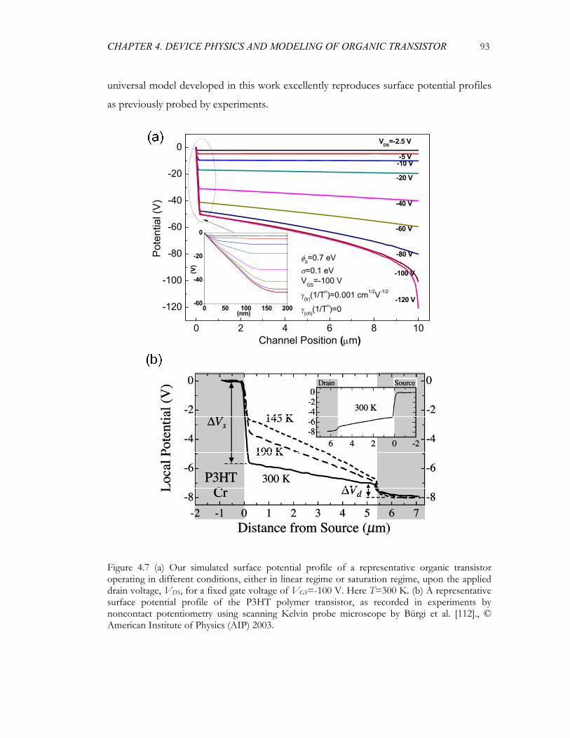
CHAPTER 4. DEVICE PHYSICS AND MODELING OF ORGANIC TRANSISTOR 93
universal model developed in this work excellently reproduces surface potential profiles
as previously probed by experiments.
0 2 4 6 8 10
-120
-100
-80
-60
-40
-20
0
0 50 100 150 200-60
-40
-20
0
φb=0.7 eVσ=0.1 eVVGS=-100 V
γ(tr)(1/Tn)=0.001 cm1/2V-1/2
γ(ch)(1/Tn)=0-120 V
-100 V
-80 V
-60 V
-40 V
-20 V
-10 V-5 V
Pote
ntia
l (V
)
Channel Position (μm)
VDS=-2.5 V
(V)
(nm)
Figure 4.7 (a) Our simulated surface potential profile of a representative organic transistor operating in different conditions, either in linear regime or saturation regime, upon the applied drain voltage, VDS, for a fixed gate voltage of VGS=-100 V. Here T=300 K. (b) A representative surface potential profile of the P3HT polymer transistor, as recorded in experiments by noncontact potentiometry using scanning Kelvin probe microscope by Bürgi et al. [112]., © American Institute of Physics (AIP) 2003.
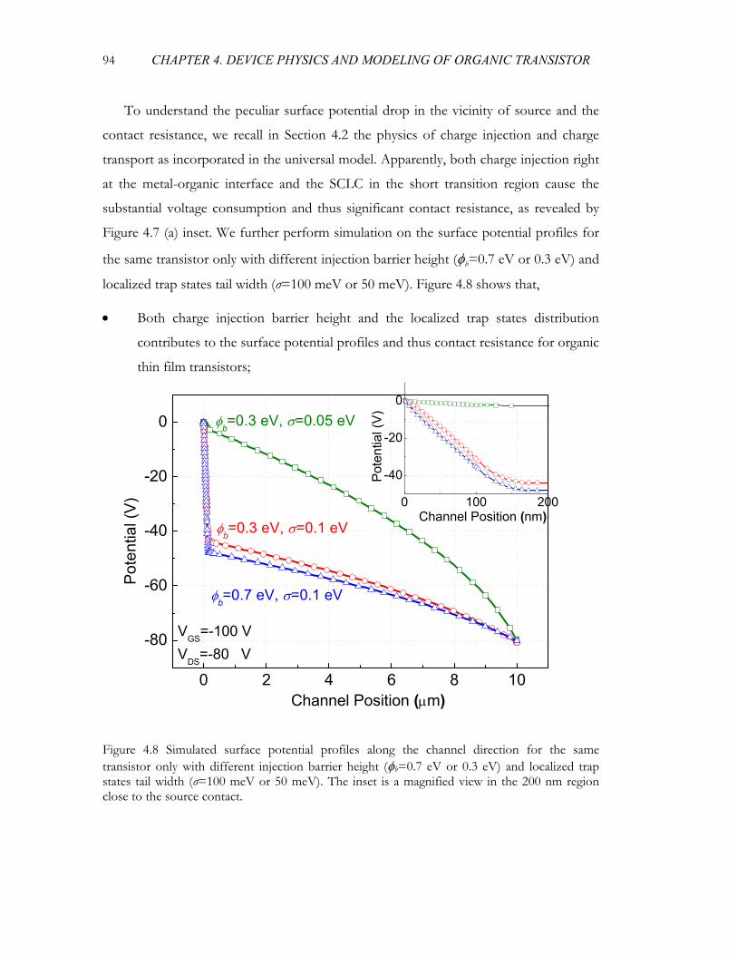
94 CHAPTER 4. DEVICE PHYSICS AND MODELING OF ORGANIC TRANSISTOR
To understand the peculiar surface potential drop in the vicinity of source and the
contact resistance, we recall in Section 4.2 the physics of charge injection and charge
transport as incorporated in the universal model. Apparently, both charge injection right
at the metal-organic interface and the SCLC in the short transition region cause the
substantial voltage consumption and thus significant contact resistance, as revealed by
Figure 4.7 (a) inset. We further perform simulation on the surface potential profiles for
the same transistor only with different injection barrier height (φb=0.7 eV or 0.3 eV) and
localized trap states tail width (σ=100 meV or 50 meV). Figure 4.8 shows that,
• Both charge injection barrier height and the localized trap states distribution
contributes to the surface potential profiles and thus contact resistance for organic
thin film transistors;
0 2 4 6 8 10
-80
-60
-40
-20
0
0 100 200
-40
-20
0
Pote
ntia
l (V)
Channel Position (μm)
VGS=-100 VVDS=-80 V
φb=0.7 eV, σ=0.1 eV
φb=0.3 eV, σ=0.1 eV
φb=0.3 eV, σ=0.05 eV
Pot
entia
l (V
)
Channel Position (nm)
Figure 4.8 Simulated surface potential profiles along the channel direction for the same transistor only with different injection barrier height (φb=0.7 eV or 0.3 eV) and localized trap states tail width (σ=100 meV or 50 meV). The inset is a magnified view in the 200 nm region close to the source contact.
CHAPTER 4. DEVICE PHYSICS AND MODELING OF ORGANIC TRANSISTOR 95
• For the same localized states distribution in the organic film, lower charge
injection barrier height at the metal-organic interface mitigates voltage drop at the
transition region and thus reduces the contact resistance. This is consistent with
the observation on output curves as shown in Figure 4.6 (a);
• Surprisingly, for the same charge injection barrier height at the metal-organic
interface, narrower localized trap states distribution, or, equivalently, smaller
Gaussian energy width of the organic film’s localized states close to the metal-
organic contacts, leads to substantially lower voltage drop in the transition region,
accordingly, giving rise to significantly reduced contact resistance. This effect is
not expected at first glance, but indeed plays a critical role in determining the
organic transistor performance as found in this study.
4.3.3 Mobility Scaling Behavior
As introduced at the beginning of this chapter, a critical issue remaining for organic
transistors is to resolve their mobility scaling behavior. By virtue of our universal
physical model in Section 4.2, we are now able to elucidate the apparently contradictory
mobility scaling features as found in experiments and reported in literature.
Figure 4.9 shows the simulation results of the mobility scaling behavior with respect
to different physical origins including carrier injection barrier height (φb), localized trap
states energy distribution (σ), Poole-Frenkel like field dependence of carrier mobility
(γ(1/Tn)), and channel length dependence of film crystallinity (γc). It is revealed that,
• Depending on the weight of the above physical effects, mobility scaling curve
with respect to the channel length (L) ranging from 100 nm to 50 µm can be
monotonically upwards, or slowly get saturated, or, surprisingly, exhibit an
overshoot region;
• Lower charge injection barrier (e.g. φb=0.3 eV vs. φb=0.7 eV), smaller localized
states distribution tail width in the transition region (e.g. σ=50 meV vs. σ=100
meV), and stronger field dependence of carrier mobility in the channel region (e.g.
96 CHAPTER 4. DEVICE PHYSICS AND MODELING OF ORGANIC TRANSISTOR
γ(ch)(1/Tn))=0 vs. γ(ch)(1/Tn))=0.01 cm1/2V-1/2) all give rise to the increase of the
extrinsic field-effect mobility (μFET).
• Importantly, large modulation of the extrinsic mobility can be realized by 1-2
orders of magnitude through engineering the charge injection barrier and the
localized states distribution at the metal-organic semiconductor interface;
• The organic transistors show an extrinsic field-effect mobility increasing
monotonically with the channel length when a large injection barrier height and a
wide disordered localization states distribution occur at the contact region, which
leads to significant extrinsic contact resistance as discussed in Section 4.3.2. Such
phenomenon is consistently observed for organic transistors with the so-called
“poor contacts” in literature [76-90], and adversely compromises the benefits
from device scaling theory as introduced at the beginning of this chapter;
• It is possible to maintain a steady extrinsic field-effect mobility at a normal
channel length above the transition region width, typically, on the level of
micrometers, given that an adequate combination of charge injection barrier
height at the metal-organic interface and localized states energy distribution in the
film is established. For instance, the simulation here shows the extrinsic mobility
is almost constant for a channel length of 5-50 µm, with an injection barrier height
of 0.3 eV and a localized trap states energy distribution width of 50 meV;
• Significantly, we discover an overshoot region that may emerge in the mobility
scaling curve for organic thin film transistors within normally fabricated device
size range, provided that the electric field dependence of carrier mobility
(γ(ch)(1/Tn)) and the channel length dependence of film crystallinity (γc) in the
channel region take strong effect. This finding is understood as follows: For short
channel devices, e.g. L=100 nm to 5 µm for the simulation shown in Figure 4.9,
the extrinsic field-effect mobility is dominated by charge injection at the contact
interface and charge transport in its neighboring transition region with a low
mobility. Therefore, shrinking the channel length equivalently enhances this
dominance and leads to a lower extrinsic mobility. However, the scenario
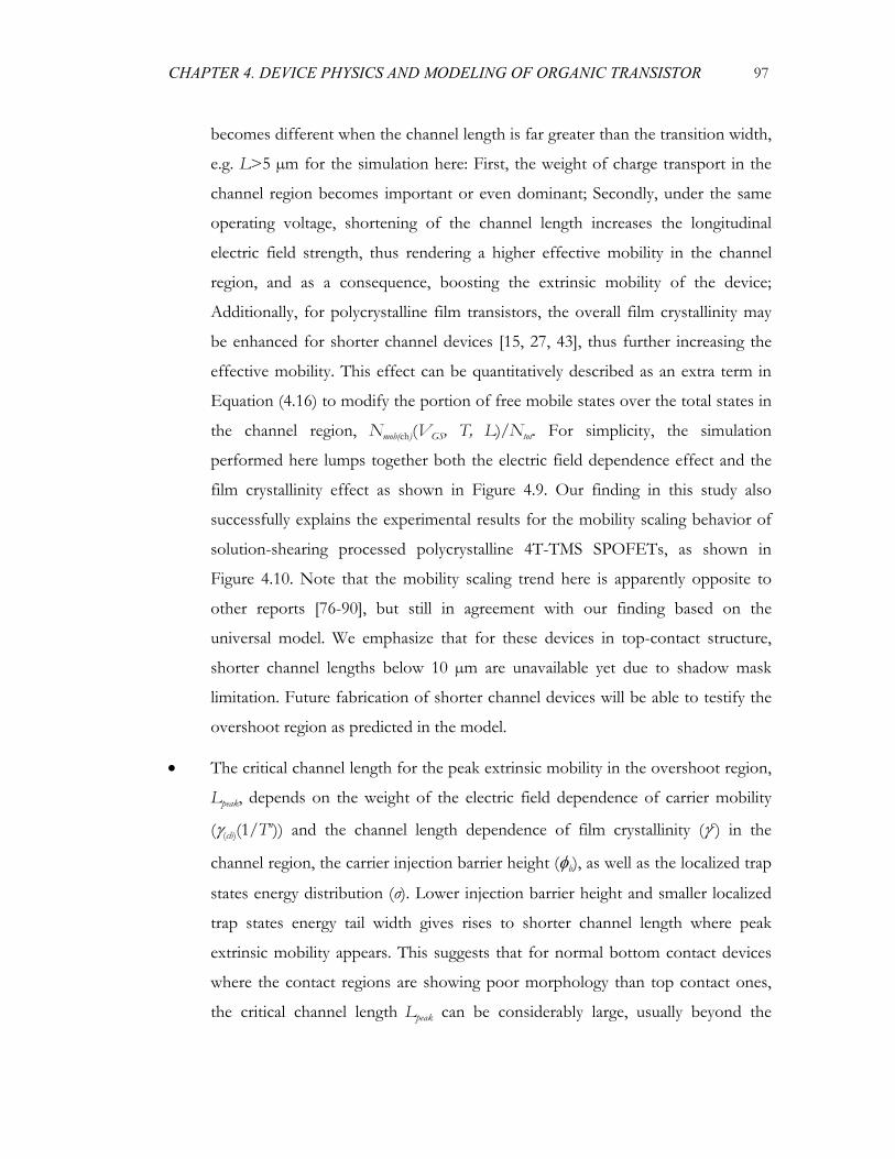
CHAPTER 4. DEVICE PHYSICS AND MODELING OF ORGANIC TRANSISTOR 97
becomes different when the channel length is far greater than the transition width,
e.g. L>5 µm for the simulation here: First, the weight of charge transport in the
channel region becomes important or even dominant; Secondly, under the same
operating voltage, shortening of the channel length increases the longitudinal
electric field strength, thus rendering a higher effective mobility in the channel
region, and as a consequence, boosting the extrinsic mobility of the device;
Additionally, for polycrystalline film transistors, the overall film crystallinity may
be enhanced for shorter channel devices [15, 27, 43], thus further increasing the
effective mobility. This effect can be quantitatively described as an extra term in
Equation (4.16) to modify the portion of free mobile states over the total states in
the channel region, Nmob(ch)(VGS, T, L)/Ntot. For simplicity, the simulation
performed here lumps together both the electric field dependence effect and the
film crystallinity effect as shown in Figure 4.9. Our finding in this study also
successfully explains the experimental results for the mobility scaling behavior of
solution-shearing processed polycrystalline 4T-TMS SPOFETs, as shown in
Figure 4.10. Note that the mobility scaling trend here is apparently opposite to
other reports [76-90], but still in agreement with our finding based on the
universal model. We emphasize that for these devices in top-contact structure,
shorter channel lengths below 10 µm are unavailable yet due to shadow mask
limitation. Future fabrication of shorter channel devices will be able to testify the
overshoot region as predicted in the model.
• The critical channel length for the peak extrinsic mobility in the overshoot region,
Lpeak, depends on the weight of the electric field dependence of carrier mobility
(γ(ch)(1/Tn)) and the channel length dependence of film crystallinity (γc) in the
channel region, the carrier injection barrier height (φb), as well as the localized trap
states energy distribution (σ). Lower injection barrier height and smaller localized
trap states energy tail width gives rises to shorter channel length where peak
extrinsic mobility appears. This suggests that for normal bottom contact devices
where the contact regions are showing poor morphology than top contact ones,
the critical channel length Lpeak can be considerably large, usually beyond the
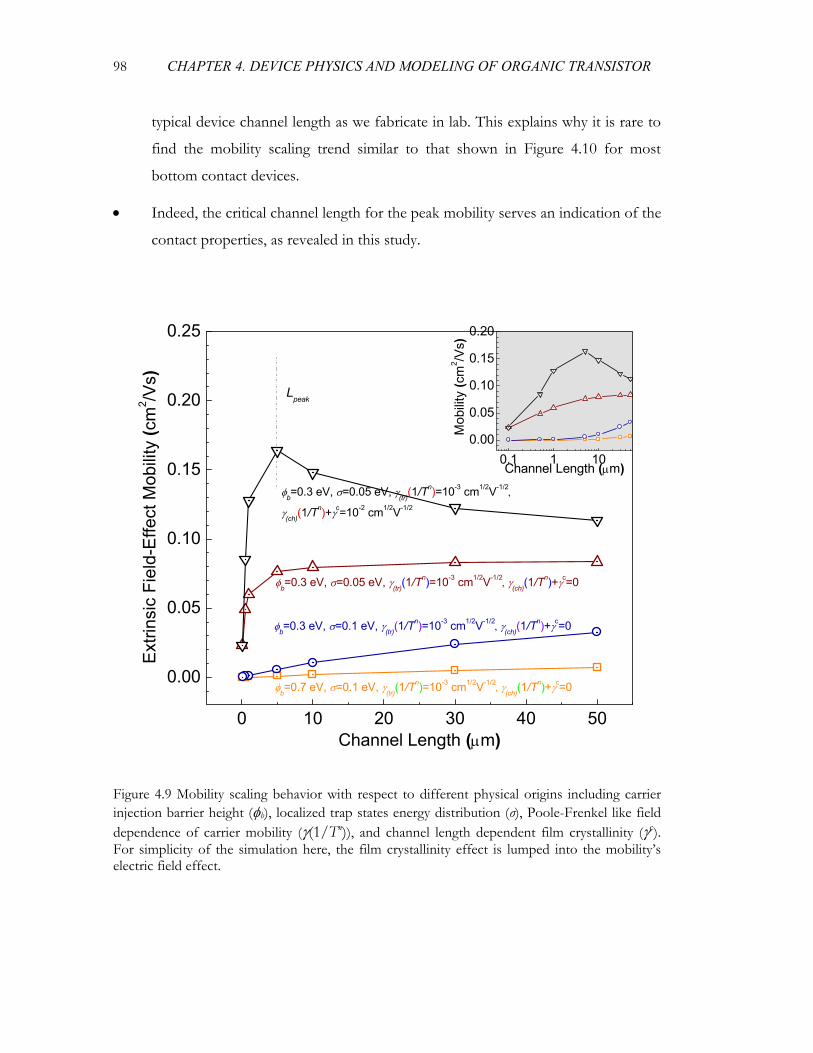
98 CHAPTER 4. DEVICE PHYSICS AND MODELING OF ORGANIC TRANSISTOR
typical device channel length as we fabricate in lab. This explains why it is rare to
find the mobility scaling trend similar to that shown in Figure 4.10 for most
bottom contact devices.
• Indeed, the critical channel length for the peak mobility serves an indication of the
contact properties, as revealed in this study.
0 10 20 30 40 50
0.00
0.05
0.10
0.15
0.20
0.25
0.1 1 100.00
0.05
0.10
0.15
0.20
Ext
rinsi
c Fi
eld-
Effe
ct M
obili
ty (c
m2 /V
s)
Channel Length (μm)
φb=0.3 eV, σ=0.05 eV, γ(tr)(1/Tn)=10-3 cm1/2V-1/2,
γ(ch)(1/Tn)+γc=10-2 cm1/2V-1/2
φb=0.3 eV, σ=0.05 eV, γ(tr)(1/Tn)=10-3 cm1/2V-1/2, γ(ch)(1/T
n)+γc=0
φb=0.3 eV, σ=0.1 eV, γ(tr)(1/Tn)=10-3 cm1/2V-1/2, γ(ch)(1/T
n)+γc=0
φb=0.7 eV, σ=0.1 eV, γ(tr)(1/Tn)=10-3 cm1/2V-1/2, γ(ch)(1/T
n)+γc=0
Lpeak
Mob
ility
(cm
2 /Vs)
Channel Length (μm)
Figure 4.9 Mobility scaling behavior with respect to different physical origins including carrier injection barrier height (φb), localized trap states energy distribution (σ), Poole-Frenkel like field dependence of carrier mobility (γ(1/Tn)), and channel length dependent film crystallinity (γc). For simplicity of the simulation here, the film crystallinity effect is lumped into the mobility’s electric field effect.
CHAPTER 4. DEVICE PHYSICS AND MODELING OF ORGANIC TRANSISTOR 99
0 10 20 30 40 500.0
0.1
0.2
0.3
0.4
0.5
Mea
sure
d E
xtrin
sic
Mob
ility
μ FET
(cm
2 /Vs)
Channel Length, L (μm)
Lpeak
Figure 4.10 Measurement results of the extrinsic field-effect mobility with respect to different channels for the solution-shearing processed polycrystalline 4T-TMS SPOFETs. The device fabrication and measurement are detailed in Chapter 2. All of these devices are fabricated on the same wafer with the same process. The dashed line is for visual guidance and refers to the modeling and simulation results shown in Figure 4.9. It is found that the finding based on our model is in excellent agreement with the experimental results.
4.4 Summary
We have developed a universal physical model for organic transistors by
incorporating both charge injection effects at the metal-organic interface and charge
transport properties in the organic semiconductor film, and successfully applied the
device model to resolve many elusive physical phenomena observed so far, such as the
peculiar mobility scaling behavior, the contact resistance effect, and the mysterious
surface potential profiles of organic transistors which have been experimentally probed
yet poorly understood. We also discovered in this study that an overshoot region may
100 CHAPTER 4. DEVICE PHYSICS AND MODELING OF ORGANIC TRANSISTOR
emerge in the mobility scaling curve with respect to the channel length. This work
provides fresh insight into understanding of the fundamental physics of organic
transistors as well as new engineering methods for improving the organic transistor
performance.
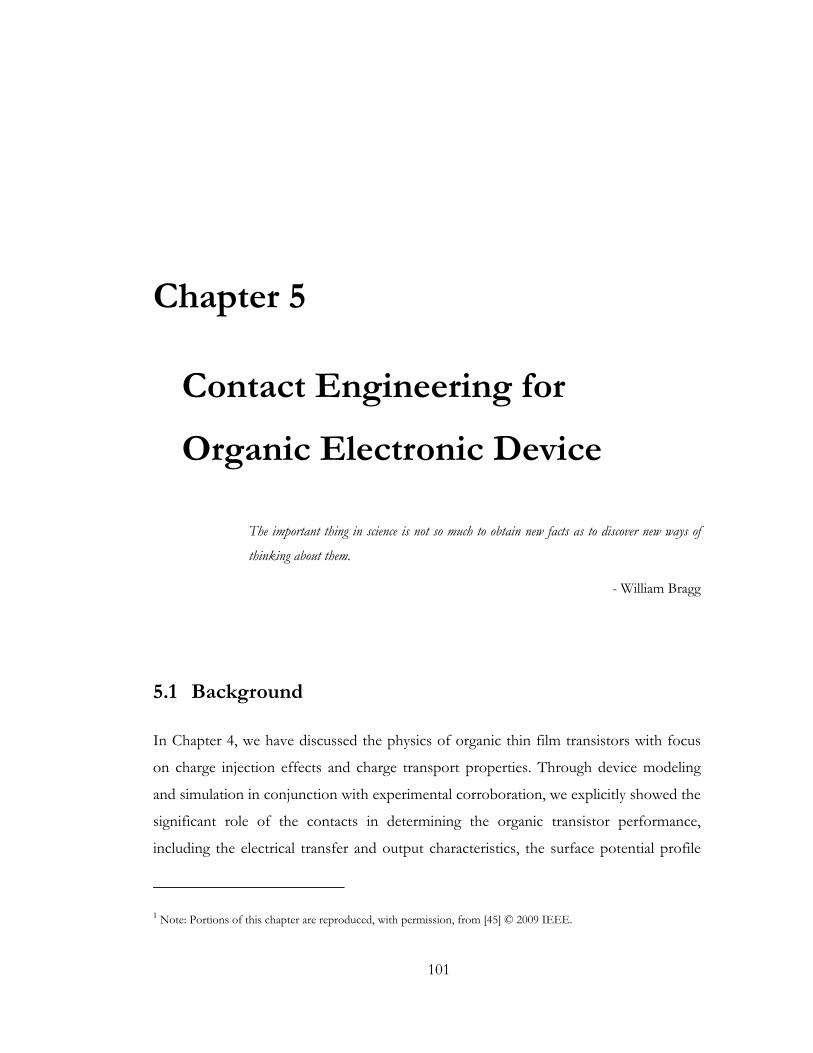
101
Chapter 5
Contact Engineering for
Organic Electronic Device
The important thing in science is not so much to obtain new facts as to discover new ways of
thinking about them.
- William Bragg
5.1 Background
In Chapter 4, we have discussed the physics of organic thin film transistors with focus
on charge injection effects and charge transport properties. Through device modeling
and simulation in conjunction with experimental corroboration, we explicitly showed the
significant role of the contacts in determining the organic transistor performance,
including the electrical transfer and output characteristics, the surface potential profile
1 Note: Portions of this chapter are reproduced, with permission, from [45] © 2009 IEEE.
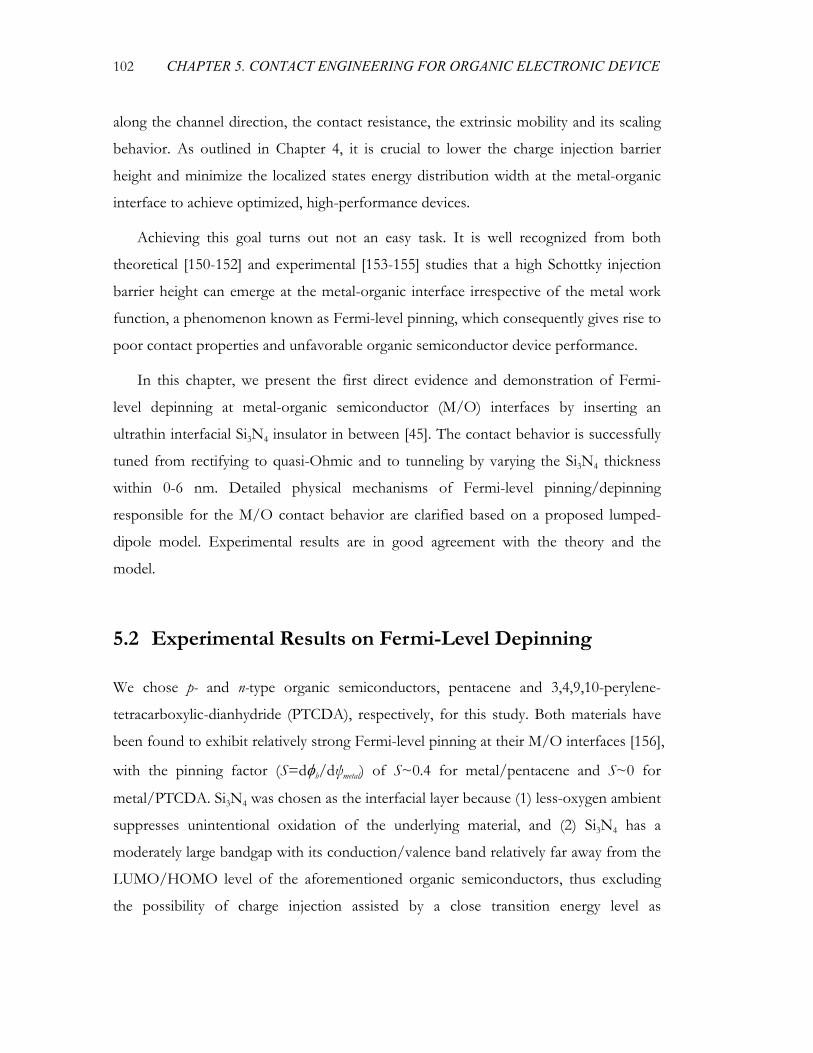
102 CHAPTER 5. CONTACT ENGINEERING FOR ORGANIC ELECTRONIC DEVICE
along the channel direction, the contact resistance, the extrinsic mobility and its scaling
behavior. As outlined in Chapter 4, it is crucial to lower the charge injection barrier
height and minimize the localized states energy distribution width at the metal-organic
interface to achieve optimized, high-performance devices.
Achieving this goal turns out not an easy task. It is well recognized from both
theoretical [150-152] and experimental [153-155] studies that a high Schottky injection
barrier height can emerge at the metal-organic interface irrespective of the metal work
function, a phenomenon known as Fermi-level pinning, which consequently gives rise to
poor contact properties and unfavorable organic semiconductor device performance.
In this chapter, we present the first direct evidence and demonstration of Fermi-
level depinning at metal-organic semiconductor (M/O) interfaces by inserting an
ultrathin interfacial Si3N4 insulator in between [45]. The contact behavior is successfully
tuned from rectifying to quasi-Ohmic and to tunneling by varying the Si3N4 thickness
within 0-6 nm. Detailed physical mechanisms of Fermi-level pinning/depinning
responsible for the M/O contact behavior are clarified based on a proposed lumped-
dipole model. Experimental results are in good agreement with the theory and the
model.
5.2 Experimental Results on Fermi-Level Depinning
We chose p- and n-type organic semiconductors, pentacene and 3,4,9,10-perylene-
tetracarboxylic-dianhydride (PTCDA), respectively, for this study. Both materials have
been found to exhibit relatively strong Fermi-level pinning at their M/O interfaces [156],
with the pinning factor (S=dφb/dψmetal) of S~0.4 for metal/pentacene and S~0 for
metal/PTCDA. Si3N4 was chosen as the interfacial layer because (1) less-oxygen ambient
suppresses unintentional oxidation of the underlying material, and (2) Si3N4 has a
moderately large bandgap with its conduction/valence band relatively far away from the
LUMO/HOMO level of the aforementioned organic semiconductors, thus excluding
the possibility of charge injection assisted by a close transition energy level as
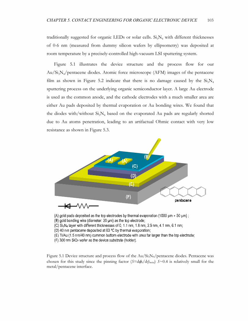
CHAPTER 5. CONTACT ENGINEERING FOR ORGANIC ELECTRONIC DEVICE 103
traditionally suggested for organic LEDs or solar cells. Si3N4 with different thicknesses
of 0-6 nm (measured from dummy silicon wafers by ellipsometry) was deposited at
room temperature by a precisely-controlled high-vacuum LSI sputtering system.
Figure 5.1 illustrates the device structure and the process flow for our
Au/Si3N4/pentacene diodes. Atomic force microscope (AFM) images of the pentacene
film as shown in Figure 5.2 indicate that there is no damage caused by the Si3N4
sputtering process on the underlying organic semiconductor layer. A large Au electrode
is used as the common anode, and the cathode electrodes with a much smaller area are
either Au pads deposited by thermal evaporation or Au bonding wires. We found that
the diodes with/without Si3N4 based on the evaporated Au pads are regularly shorted
due to Au atoms penetration, leading to an artifactual Ohmic contact with very low
resistance as shown in Figure 5.3.
Figure 5.1 Device structure and process flow of the Au/Si3N4/pentacene diodes. Pentacene was chosen for this study since the pinning factor (S=dφb/dψmetal) S~0.4 is relatively small for the metal/pentacene interface.
104 CHAPTER 5. CONTACT ENGINEERING FOR ORGANIC ELECTRONIC DEVICE
Figure 5.2 AFM images of 200 nm pentacene films deposited on Au at room temperature (a) before and (b) after Si3N4 sputtering deposition. Height scale: 300 nm.
-0.6 -0.4 -0.2 0.0 0.2 0.4 0.6
-200
-100
0
100
200
Curre
nt d
ensit
y (A/
cm2 )
Voltage (V)
t(SiN)=4.1 nm t(SiN)=2.9 nm t(SiN)=1.1 nm
Figure 5.3 I-V measurement results showing the diodes with/without Si3N4 based on evaporated Au pads are regularly shorted due to metal atoms penetration along the grain boundaries or the roughness-induced vacancies.
To resolve the shorting issues and eliminate the electrical artifacts resulting from the
gold atom penetration, we introduced the gold wire based diode configurations for this
study as depicted in Figure 5.1. Figure 5.4 shows the measured I-V characteristics of the
Au/Si3N4/pentacene diodes with different Si3N4 thicknesses, providing direct evidence
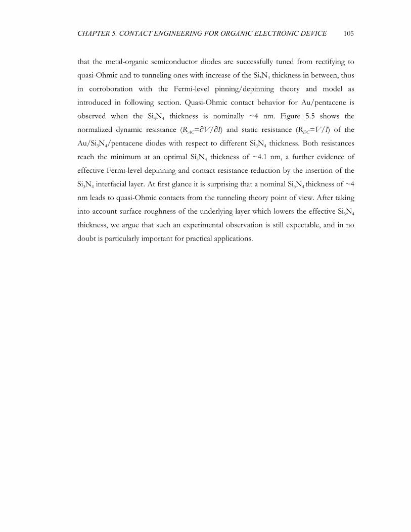
CHAPTER 5. CONTACT ENGINEERING FOR ORGANIC ELECTRONIC DEVICE 105
that the metal-organic semiconductor diodes are successfully tuned from rectifying to
quasi-Ohmic and to tunneling ones with increase of the Si3N4 thickness in between, thus
in corroboration with the Fermi-level pinning/depinning theory and model as
introduced in following section. Quasi-Ohmic contact behavior for Au/pentacene is
observed when the Si3N4 thickness is nominally ~4 nm. Figure 5.5 shows the
normalized dynamic resistance (RAC=∂V/∂I) and static resistance (RDC=V/I) of the
Au/Si3N4/pentacene diodes with respect to different Si3N4 thickness. Both resistances
reach the minimum at an optimal Si3N4 thickness of ~4.1 nm, a further evidence of
effective Fermi-level depinning and contact resistance reduction by the insertion of the
Si3N4 interfacial layer. At first glance it is surprising that a nominal Si3N4 thickness of ~4
nm leads to quasi-Ohmic contacts from the tunneling theory point of view. After taking
into account surface roughness of the underlying layer which lowers the effective Si3N4
thickness, we argue that such an experimental observation is still expectable, and in no
doubt is particularly important for practical applications.
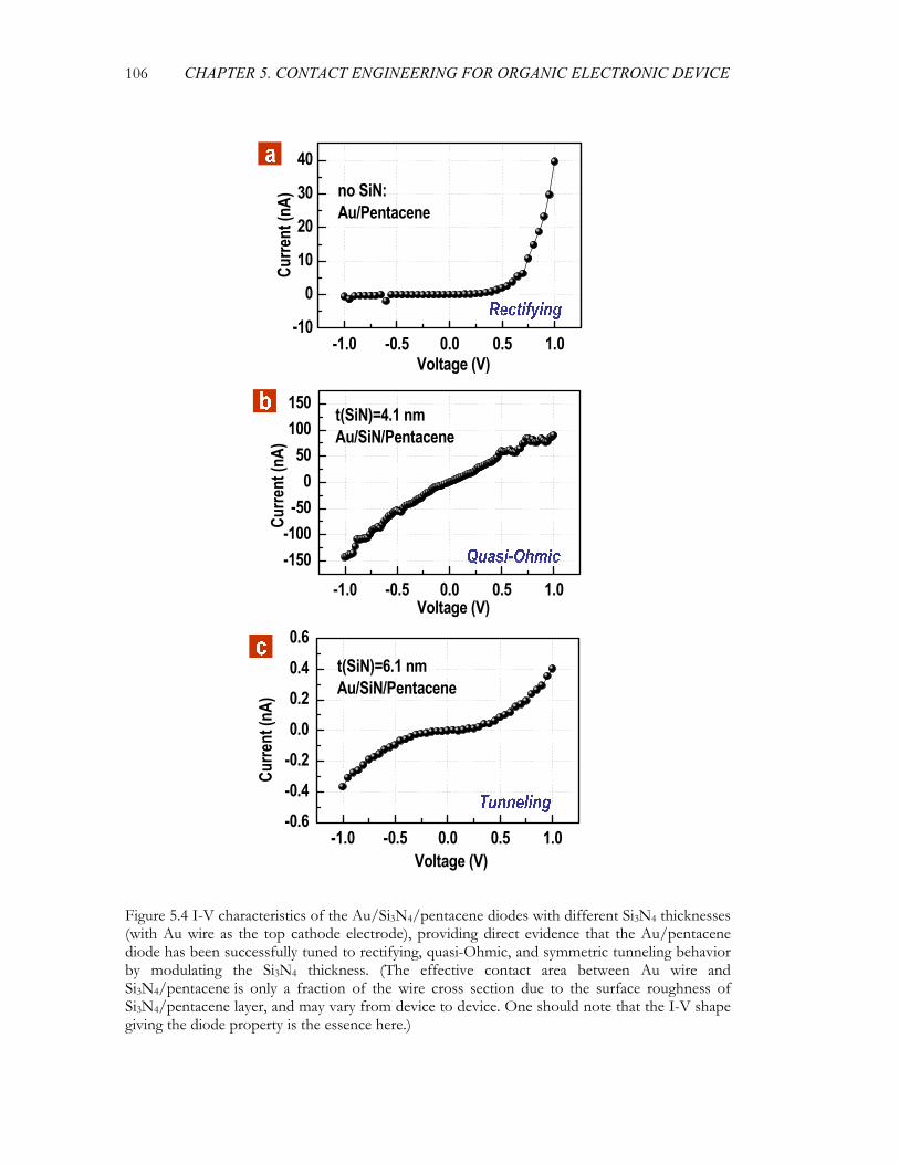
106 CHAPTER 5. CONTACT ENGINEERING FOR ORGANIC ELECTRONIC DEVICE
-1.0 -0.5 0.0 0.5 1.0-150-100-50
050
100150
t(SiN)=4.1 nmAu/SiN/Pentacene
Voltage (V)
Curre
nt (n
A)
-1.0 -0.5 0.0 0.5 1.0-10
0
10
20
30
40
Curre
nt (n
A)
Voltage (V)
no SiN:Au/Pentacene
-1.0 -0.5 0.0 0.5 1.0-0.6-0.4-0.20.00.20.40.6
t(SiN)=6.1 nmAu/SiN/Pentacene
Voltage (V)
Curre
nt (n
A)
Figure 5.4 I-V characteristics of the Au/Si3N4/pentacene diodes with different Si3N4 thicknesses (with Au wire as the top cathode electrode), providing direct evidence that the Au/pentacene diode has been successfully tuned to rectifying, quasi-Ohmic, and symmetric tunneling behavior by modulating the Si3N4 thickness. (The effective contact area between Au wire and Si3N4/pentacene is only a fraction of the wire cross section due to the surface roughness of Si3N4/pentacene layer, and may vary from device to device. One should note that the I-V shape giving the diode property is the essence here.)
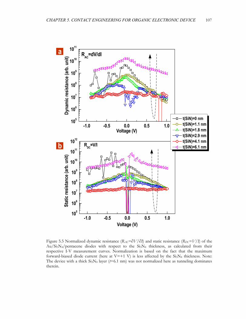
CHAPTER 5. CONTACT ENGINEERING FOR ORGANIC ELECTRONIC DEVICE 107
-1.0 -0.5 0.0 0.5 1.0105
106
107
108
109
1010
1011
1012
Stat
ic re
sista
nce (
arb.
uni
t)
Voltage (V)
RDC=V/I
-1.0 -0.5 0.0 0.5 1.0105
106
107
108
109
1010
1011
t(SiN)=0 nm t(SiN)=1.1 nm t(SiN)=1.8 nm t(SiN)=2.9 nm t(SiN)=4.1 nm t(SiN)=6.1 nm
RAC=dV/dI
Dyna
mic
resis
tanc
e (ar
b. u
nit)
Voltage (V)
(b)b
a
Figure 5.5 Normalized dynamic resistance (RAC=∂V/∂I) and static resistance (RDC=V/I) of the Au/Si3N4/pentacene diodes with respect to the Si3N4 thickness, as calculated from their respective I-V measurement curves. Normalization is based on the fact that the maximum forward-biased diode current (here at V=+1 V) is less affected by the Si3N4 thickness. Note: The device with a thick Si3N4 layer (t=6.1 nm) was not normalized here as tunneling dominates therein.
108 CHAPTER 5. CONTACT ENGINEERING FOR ORGANIC ELECTRONIC DEVICE
We also fabricated Ag/Si3N4/PTCDA diode array as shown in Figure 5.6 for this
study. Instead of measuring an individual diode’s I-V curve, here we evaluated the
contact resistance of Ag/Si3N4/PTCDA by measuring two back-to-back diodes in series
connection with a low-conductivity PTCDA bulk film [see Figure 5.7 (a)]. Figure 5.7 (b)
shows explicitly a minimum contact resistance observed for the Ag/PTCDA interface
with an optimal sandwiched Si3N4 thickness of ~2.5 nm, reaffirming the Fermi-level
depinning at M/O interfaces by inserting the ultrathin Si3N4 interfacial layer. The
apparent difference of the optimal Si3N4 thickness for Au/pentacene and Ag/PTCDA
interfaces can be attributed to their different interface roughness (and thus different
effective interfacial layer thickness). This also underscores that one should consider the
particular device structure and materials therein when applying the Fermi-level
depinning technology to high performance organic devices.
(A) (A)(B)
(C)
(D)
(A) (A)
(A) Ag electrode array with thickness=30 nm and spacing=250 μm acting as bottom electrodes; (B) Si3N4 layer with different thicknesses of 0.6 nm, 1.0 nm, 1.9 nm, 2.4 nm, 3.2 nm, 3.9 nm, 6.1 nm; (C) 130 nm PTCDA deposited at room temperature by thermal evaporation;(D) 300 nm SiO2 wafer as the device substrate (holder).
O
OO
O
OO
PTCDA
(A) (B) (C)
1mm
Figure 5.6 Device structure, microscopy image, and process flow of the Ag/Si3N4/PTCDA diodes. PTCDA was chosen here since the pinning factor (S=dφb/dψmetal) is S~0 for metal/PTCDA interface, indicating very strong Fermi-level pinning effect at the metal/PTCDA interface.
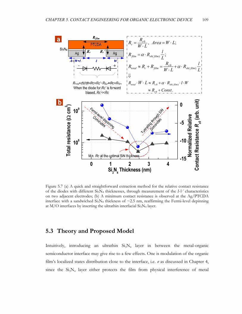
CHAPTER 5. CONTACT ENGINEERING FOR ORGANIC ELECTRONIC DEVICE 109
0 ( )
0
0
( )
0( )
,
.
;
;
total c sh film
c
cc
film sh film
cctotal film sh film
R R R l W
R Const
RR Area W LW L
lR RL
R lR R R RW L L
W L α
α
α
⇓⋅ ≈ + ⋅ ⋅ ⋅
≈ +
= = ⋅⋅
= ⋅
≈ + = + ⋅⋅
⋅
0 1 2 3 4
108
109
-15
-10
-5
0
To
tal r
esist
ance
(Ω cm
2 )
Si3N4 Thickness (nm)
Norm
alize
d Re
lative
Co
ntac
t Res
istan
ce Rc0
(arb
. uni
t)
Figure 5.7 (a) A quick and straightforward extraction method for the relative contact resistance of the diodes with different Si3N4 thicknesses, through measurement of the I-V characteristics on two adjacent electrodes; (b) A minimum contact resistance is observed at the Ag/PTCDA interface with a sandwiched Si3N4 thickness of ~2.5 nm, reaffirming the Fermi-level depinning at M/O interfaces by inserting the ultrathin interfacial Si3N4 layer.
5.3 Theory and Proposed Model
Intuitively, introducing an ultrathin Si3N4 layer in between the metal-organic
semiconductor interface may give rise to a few effects. One is modulation of the organic
film’s localized states distribution close to the interface, i.e. σ as discussed in Chapter 4,
since the Si3N4 layer either protects the film from physical interference of metal
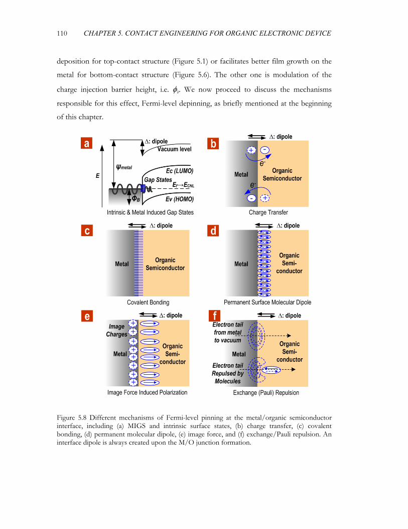
110 CHAPTER 5. CONTACT ENGINEERING FOR ORGANIC ELECTRONIC DEVICE
deposition for top-contact structure (Figure 5.1) or facilitates better film growth on the
metal for bottom-contact structure (Figure 5.6). The other one is modulation of the
charge injection barrier height, i.e. φb. We now proceed to discuss the mechanisms
responsible for this effect, Fermi-level depinning, as briefly mentioned at the beginning
of this chapter.
Figure 5.8 Different mechanisms of Fermi-level pinning at the metal/organic semiconductor interface, including (a) MIGS and intrinsic surface states, (b) charge transfer, (c) covalent bonding, (d) permanent molecular dipole, (e) image force, and (f) exchange/Pauli repulsion. An interface dipole is always created upon the M/O junction formation.
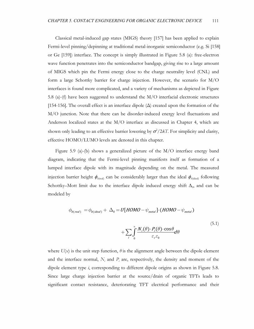
CHAPTER 5. CONTACT ENGINEERING FOR ORGANIC ELECTRONIC DEVICE 111
Classical metal-induced gap states (MIGS) theory [157] has been applied to explain
Fermi-level pinning/depinning at traditional metal-inorganic semiconductor (e.g. Si [158]
or Ge [159]) interface. The concept is simply illustrated in Figure 5.8 (a): free-electron
wave function penetrates into the semiconductor bandgap, giving rise to a large amount
of MIGS which pin the Fermi energy close to the charge neutrality level (CNL) and
form a large Schottky barrier for charge injection. However, the scenario for M/O
interfaces is found more complicated, and a variety of mechanisms as depicted in Figure
5.8 (a)-(f) have been suggested to understand the M/O interfacial electronic structures
[154-156]. The overall effect is an interface dipole (Δ) created upon the formation of the
M/O junction. Note that there can be disorder-induced energy level fluctuations and
Anderson localized states at the M/O interface as discussed in Chapter 4, which are
shown only leading to an effective barrier lowering by σ2/2kT. For simplicity and clarity,
effective HOMO/LUMO levels are denoted in this chapter.
Figure 5.9 (a)-(b) shows a generalized picture of the M/O interface energy band
diagram, indicating that the Fermi-level pinning manifests itself as formation of a
lumped interface dipole with its magnitude depending on the metal. The measured
injection barrier height φb(real) can be considerably larger than the ideal φb(ideal) following
Schottky–Mott limit due to the interface dipole induced energy shift ∆0, and can be
modeled by
0
00
cos
b real b ideal metal metal
i i
i r
U HOMO HOMO
N P dπ
φ φ ψ ψ
θ θ θ θε ε
= + Δ = − ⋅ −
⋅ ⋅+∑∫ (5.1)
where U(x) is the unit step function, θ is the alignment angle between the dipole element
and the interface normal, Ni and Pi are, respectively, the density and moment of the
dipole element type i, corresponding to different dipole origins as shown in Figure 5.8.
Since large charge injection barrier at the source/drain of organic TFTs leads to
significant contact resistance, deteriorating TFT electrical performance and their
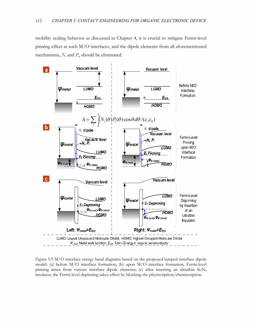
112 CHAPTER 5. CONTACT ENGINEERING FOR ORGANIC ELECTRONIC DEVICE
mobility scaling behavior as discussed in Chapter 4, it is crucial to mitigate Fermi-level
pinning effect at such M/O interfaces, and the dipole elements from all aforementioned
mechanisms, Ni and Pi, should be eliminated.
00
( ) ( ) cos /( )i i ri
N P dπ
θ θ θ θ ε εΔ = ∑∫
Figure 5.9 M/O interface energy band diagrams based on the proposed lumped interface dipole model: (a) before M/O interface formation; (b) upon M/O interface formation, Fermi-level pinning arises from various interface dipole elements; (c) after inserting an ultrathin Si3N4 insulator, the Fermi-level depinning takes effect by blocking the physisorption/chemisorption.
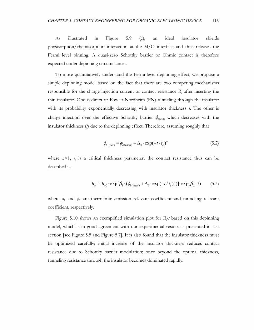
CHAPTER 5. CONTACT ENGINEERING FOR ORGANIC ELECTRONIC DEVICE 113
As illustrated in Figure 5.9 (c), an ideal insulator shields
physisorption/chemisorption interaction at the M/O interface and thus releases the
Fermi level pinning. A quasi-zero Schottky barrier or Ohmic contact is therefore
expected under depinning circumstances.
To more quantitatively understand the Fermi-level depinning effect, we propose a
simple depinning model based on the fact that there are two competing mechanisms
responsible for the charge injection current or contact resistance Rc after inserting the
thin insulator. One is direct or Fowler-Nordheim (FN) tunneling through the insulator
with its probability exponentially decreasing with insulator thickness t. The other is
charge injection over the effective Schottky barrier φb(real) which decreases with the
insulator thickness (t) due to the depinning effect. Therefore, assuming roughly that
( ) ( ) 0 exp( / )nb real b ideal ct tφ φ= + Δ ⋅ − (5.2)
where n>1, tc is a critical thickness parameter, the contact resistance thus can be
described as
0 1 ( ) 0 2exp[ ( exp( / ) )] exp( )nc c b ideal cR R t t tβ φ β≅ ⋅ ⋅ + Δ ⋅ − ⋅ ⋅ (5.3)
where β1 and β2 are thermionic emission relevant coefficient and tunneling relevant
coefficient, respectively.
Figure 5.10 shows an exemplified simulation plot for Rc-t based on this depinning
model, which is in good agreement with our experimental results as presented in last
section [see Figure 5.5 and Figure 5.7]. It is also found that the insulator thickness must
be optimized carefully: initial increase of the insulator thickness reduces contact
resistance due to Schottky barrier modulation; once beyond the optimal thickness,
tunneling resistance through the insulator becomes dominated rapidly.
114 CHAPTER 5. CONTACT ENGINEERING FOR ORGANIC ELECTRONIC DEVICE
Figure 5.10 Simulation results based on the proposed simple depinning model showing the dominant mechanisms responsible for the contact resistance behavior after insertion of the ultrathin insulating layer at the M/O interface.
5.4 Summary
We have successfully demonstrated Fermi-level depinning at two different M/O
interfaces by inserting a precisely-controlled ultrathin interfacial Si3N4 layer. The contact
behavior is tuned from rectifying to quasi-Ohmic and to tunneling by modulation of the
CHAPTER 5. CONTACT ENGINEERING FOR ORGANIC ELECTRONIC DEVICE 115
Si3N4 thickness within 0-6 nm. We also proposed a lumped dipole model to clarify the
detailed physical mechanisms of Fermi-level pinning/depinning at the M/O interface.
Experimental results are in good agreement with the theory and the model. This work
represents a significant step toward the fundamental understanding of M/O interface
properties and technological advancement of achieving low-resistance Ohmic contacts
for organic electronic device applications, and can be particularly useful for optimization
of the organic transistor performance through source/drain contact engineering.

116 CHAPTER 5. CONTACT ENGINEERING FOR ORGANIC ELECTRONIC DEVICE
117
Chapter 6
Conclusions and Outlook
Give me a fulcrum, and I shall move the world.
- Archimedes of Syracuse (Ἀρχιμήδης)
In this dissertation, we have systematically studied carbon or organic semiconductor
thin-film field-effect transistors, particularly, solution-processed organic field-effect
transistors (SPOFETs), toward application in the emerging flexible electronics and
macroelectronics fields. The topics described span from fundamental device physics,
device modeling, fabrication technology to interface/contact engineering, highlighting
the most important aspects for the development of organic transistor based electronic
devices and systems.
6.1 Conclusions
Revisit the dissertation, there are a number of research contributions originated from
this work. A brief summary of the contributions here serves as the conclusions of this
dissertation.
118 CHAPTER 6. CONCLUSIONS AND OUTLOOK
• Designed a novel device architecture for flexible SPOFETs; Demonstrated and
characterized high performance flexible SPOFETs on plastic with a carrier
mobility over 0.2 cm2/Vs, a turn-on voltage of near 0 V, and a record low
subthreshold slope of ~80 mV/dec in ambient conditions. These exceptional
characteristics are achieved by excellent electrostatic control, 3-D statistical
modeling for solution-shearing process optimization, and phenyl-terminated self-
assembled monolayer (SAM) based interface engineering.
• Utilized 3-D statistical modeling and data analysis to optimize the solution-
shearing process; Provided a general guideline of process optimization for high
performance organic transistors.
• Systematically investigated dipole moment related physical effects and chemistry
effects of the SAM at the organic semiconductor-dielectric interface; Elucidated
how the performance and reliability of organic transistors are controlled by their
interface conditions through careful selection of a group of phenyl-terminated
SAMs; Proposed electric shielding tensors effect induced by SAM dipole as a new
physical mechanism involved in the performance control of organic transistors.
• Introduced a simple spin-coating process for deposition of high-quality phenyl-
terminated SAMs for organic electronics applications.
• Proposed and developed a universal physical model and 1-D device simulator for
organic transistors by incorporating both charge injection effects at the metal-
organic interface and charge transport properties in the organic semiconductor
film; Successfully applied the device model to resolve many elusive physical
phenomena observed so far, such as the peculiar mobility scaling behavior, the
contact resistance effect, and the mysterious surface potential profiles along the
channel which have been experimentally probed yet poorly understood; Validated
the model by excellent agreement between the simulation results and the
experimental results.
• Systematically elucidated the device physics involved in the charge injection and
charge transport in organic semiconductor thin-film transistors; Discovered an
CHAPTER 6. CONCLUSIONS AND OUTLOOK 119
overshoot region in the mobility scaling behavior and identified the existence of a
critical channel length for the peak field-effect mobility.
• Explored and demonstrated Fermi-level depinning at the metal-organic interface
for low-resistance Ohmic contacts by inserting an ultrathin interfacial Si3N4
insulator in between, which lowers charge injection barrier and reduces the
interfacial disorder width or localization states; Successfully tuned the contact
behavior from rectifying to quasi-Ohmic and to tunneling by varying the Si3N4
thickness within 0-6 nm;
• Clarified the detailed physical mechanisms of Fermi-level pinning/depinning
responsible for the metal-organic semiconductor contact behavior based on a
proposed lumped-dipole model.
6.2 Outlook
There is never an end to the evolution of science and technology itself. Despite the fact
that encouraging progress has been achieved as of today in the development of organic
semiconductor transistors, many challenges and thus opportunities remain in future
studies. For the work presented in this dissertation, we address the relevant future
directions as follows.
• For the solution-shearing process described in Chapter 2, we have performed
systematical experiment design and 3-D statistical data modeling/analysis to find
out the optimal processing conditions. Indeed, it is possible to develop an
analytical model for this process and numerically simulate the growth output
based on the evaporation kinetics and crystallization kinetics. This would require
more knowledge of parameter values for the involved materials and environments.
• Based on the high-performance flexible SPOFETs introduced in Chapter 2, it is
feasible to demonstrate flexible integrated circuits and systems and bring the
flexible organic transistors closer to practical applications. A particularly
120 CHAPTER 6. CONCLUSIONS AND OUTLOOK
interesting design would be integration of the SPOFET and OLED on a single
flexible substrate for all-organic displays.
• As briefly mentioned at the end of Chapter 3, there is an important physical effect
of the SAM at the dielectric-semiconductor interface has not been considered yet
to date, i.e. strong external interfacial electric field as induced by the gate voltage
would distort the inherent dipole moment of the SAM molecule as illustrated in
Figure 3.19, thus influence the performance and reliability of organic transistors.
This effect, namely electric shielding tensors effect, must be given careful
consideration in future studies. From the experiment point of view, in-situ and
real-time measurement of the SAM dipole on an oxide surface under the applied
external electric field would testify and give direct evidence of the electric
shielding tensors effect. In the meantime, it is also possible to model this effect
using Ab-initio simulation.
• Finally, it is possible to upgrade current 1-D universal device model and device
simulator as introduced in Chapter 4 to a 2-D or 3-D simulator in the future.
121
Appendix A
Spin-coating Process for Phenyl-
Terminated Self-Assembled
Monolayer
A.1 Summary
Use simple spin-coating method to deposit high-quality, densely packed phenyl-
terminated self-assembled monolayers (SAM) on various oxides or OH-terminated
polymeric dielectric surfaces. The resultant SAMs can be used for organic electronic
devices including OFETs and diodes (particularly useful for solution-processed organic
electronics since the phenyl-SAMs possess ideal tradeoff between surface energy and
wettability for organic semiconductor solution). The electrical performance of these
devices can be superior to those based on the same phenyl-SAMs deposited by
traditional methods such as soaking.
122 APPENDIX A. SPIN-COATING PROCESS FOR PHENYL-TERMINATED SAM
A.2 Materials
(1) Phenyl-terminated silanes, such as Phenyltrichlorosilane (PTS),
Phenethyltrichlorosilane (PETS), 4-Phenylbutyltrichlorosilane (PBTS), 6-
Phenylhexyltrichlorosilane (PHTS), N-Phenylaminopropyltricholorosilane (PAPTS).
[Note: In this work, these materials were ordered from Gelest, Inc.]
(2) Anhydrous toluene
A.3 Tools
(1) Inert environment such as N2 glovebox or glovebag
(2) Spin-coater in ambient conditions
(3) Accessories such as pipettes, tips, syringes and vials
A.4 Substrate Preparation
(1) Prepare and clean substrates: for Si/SiO2 substrate, use piranha treatment (7:3
mixture of H2SO4 and H2O2, highly corrosive and oxidizing);
(2) Pre-treat substrate right before spin-coating: for piranha treated Si/SiO2
substrates, put them in UV-Ozone for 30 mins to 1 hr.
A.5 Phenyl-SAM Solution Preparation
(1) Transfer phenyl-silanes and anhydrous toluene to an inert environment, such as
N2 glovebox or glovebag; other accessories such as pipettes, tips, syringes and vials
should be transferred in all together.
APPENDIX A. SPIN-COATING PROCESS FOR PHENYL-TERMINATED SAM 123
[Note: the phenyl-silane solution in their original stock bottles should be completely clear otherwise it
has been probably polymerized. Please check this carefully. Polymerization of the original phenyl-silane
solution could significantly affect the final SAM quality]
(2) Prepare phenyl-SAM solution in anhydrous toluene in the inert environment: the
phenyl-SAM solution concentration is typically 1-1.5:1000=phenyl-silane:anhydrous
toluene by volume.
(3) Start by filtering the anhydrous toluene through a 0.2 µM filter into a 20 ml vial;
transfer 1-2 ml phenyl-silane solution from their original stock bottle into another vial
and close the original stock bottle lid immediately to minimize contamination for future
use. Prepare the phenyl-SAM solution with the appropriate concentration indicated
above from those vials.
(4) Transfer the prepared SAM solution in anhydrous toluene from the inert
glovebox/glovebag to outside.
A.6 Spin-coating for Phenyl-SAM Devices
(1) Prepare the spin-coating setup: Clean the spin-coater holder with appropriate
solvents; set the spin-rate to 3 Krpm, acceleration rate to 0.
(2) Spin-coat phenyl-SAMs on the device substrates: place the device substrate
prepared in “step-[A.4]” on the spin-coater holder; use pipette to place the phenyl-SAM
solution prepared in “step-[A.5]” onto the device substrate; make sure the solution
cover the whole substrate surface completely; wait for 10-15 secs; start spin-coating at 3
Krm for another 45-50 secs.
[Note: Please try to make the solution cover the whole substrate surface by once to minimize extra
polymerization in air. Typically a 150 uL volume of SAM solution should be used for a substrate size
of 1-4 cm2. Immediately recap the solution after each drop]
124 APPENDIX A. SPIN-COATING PROCESS FOR PHENYL-TERMINATED SAM
A.7 Post-processing
(1) Place the device substrates after spin-coating of the phenyl-SAMs in a large
desiccator or brown glass bottle. Make sure the desiccator or brown glass bottle are
clean inside to avoid contamination to the wafer backside. The contamination can bring
defects to the SAM surface during the subsequent sonication process.
(2) Prepare ~1 mL of Hydrochloric Acid (HCl) into a small 2 mL vial; place this 2
mL vial with HCl into a 20 mL vial that has been half-full with the small silica particles
used in column purification; leave both vials uncapped; place these vials into the large
desiccator or brown bottle which have samples inside; tightly close lid to the descicator
or brown bottle. Leave them undisturbed for 24-48 hrs, or at least overnight.
(3) Open the desiccator or brown bottle in the hood for safety. Remove samples and
copiously rinse with HCLP toluene; place samples in glass-ware and sonicate for 5 mins
TWICE with each solvent in the following order: (HCLP-level) Toluene, Acetone,
Isopropyl Alcohol.; dry clean with N2 gun.
(4) Store samples. Rinse the samples with the solvents and dry with N2 every time
before the use.
A.8 Reference
Y. Ito, et al., "Crystalline Ultrasmooth Self-Assembled Monolayers of Alkylsilanes
for Organic Field-Effect Transistors," Journal of the American Chemical Society, vol. 131, pp.
9396-9404, Jul 8 2009.
H. Y. Nie, et al., "Delivering octadecylphosphonic acid self-assembled monolayers
on a Si wafer and other oxide surfaces," Journal of Physical Chemistry B, vol. 110, pp.
21101-21108, Oct 26 2006.
125
Bibliography
[1] D. J. Frank, et al., "Device scaling limits of Si MOSFETs and their application
dependencies," Proceedings of the IEEE, vol. 89, pp. 259-288, Mar 2001.
[2] P. Avouris, et al., "Carbon-based electronics," Nature Nanotechnology, vol. 2, pp.
605-615, 2007.
[3] T. Durkop, et al., "Extraordinary mobility in semiconducting carbon nanotubes,"
Nano Letters, vol. 4, pp. 35-39, 2003.
[4] Y.-M. Lin, et al., "Operation of graphene transistors at gigahertz frequencies,"
Nano Letters, vol. 9, pp. 422-426, 2008.
[5] Z. Chen, et al., "An integrated logic circuit assembled on a single carbon
nanotube," Science, vol. 311, p. 1735, March 2006.
[6] Z. Bao and J. Locklin (Eds.), Organic Field-Effect Transistors. Boca Raton, FL: CRC
Press, Taylor & Francis Group, 2007.
[7] R. A. Street, "Thin-film transistors," Advanced Materials, vol. 21, pp. 2007-2022,
May 2009.
[8] S. R. Forrest, "The path to ubiquitous and low-cost organic electronic appliances
on plastic," Nature, vol. 428, pp. 911-918, Apr 2004.
[9] S. Liu, et al., "Controlled deposition of crystalline organic semiconductors for
field-effect-transistor applications," Advanced Materials, vol. 21, pp. 1217-1232,
2009.
[10] G. E. Jabbour, et al., "Screen printing for the fabrication of organic light-emitting
devices," IEEE Journal of Selected Topics in Quantum Electronics, vol. 7, pp. 769-773,
2001.
126 BIBLIOGRAPHY
[11] T. Sekitani, et al., "Organic transistors manufactured using inkjet technology with
subfemtoliter accuracy," Proceedings of the National Academy of Sciences, vol. 105, pp.
4976-4980, Apr 2008.
[12] H. Sirringhaus, et al., "High-resolution inkjet printing of all-polymer transistor
circuits," Science, vol. 290, pp. 2123-2126, Dec 2000.
[13] V. Subramanian, et al., "Progress Toward Development of All-Printed RFID
Tags: Materials, Processes, and Devices," Proceedings of the IEEE, vol. 93, pp.
1330-1338, 2005.
[14] J. A. Rogers, et al., "Paper-like electronic displays: Large-area rubber-stamped
plastic sheets of electronics and microencapsulated electrophoretic inks,"
Proceedings of the National Academy of Sciences of the United States of America, vol. 98,
pp. 4835-4840, Apr 2001.
[15] Z. Liu, et al., "Experimental study and statistical analysis of solution-shearing
processed organic transistors based on an asymmetric small-molecule
semiconductor," IEEE Transactions on Electron Devices, vol. 56, pp. 176-185, Feb
2009.
[16] D. H. Kim, et al., "High-mobility organic transistors based on single-crystalline
microribbons of triisopropylsilylethynyl pentacene via solution-phase self-
assembly," Advanced Materials, vol. 19, pp. 678-682, 2007.
[17] S. C. B. Mannsfeld, et al., "Highly efficient patterning of organic single-crystal
transistors from the solution phase," Advanced Materials, vol. 20, pp. 4044-4048,
2008.
[18] H. Klauk, "Organic circuits on flexible substrates," in Technical Digest of IEEE
International Electron Devices Meeting (IEDM), 2005, pp. 446-449.
[19] H. Sirringhaus, "Device Physics of Solution-Processed Organic Field-Effect
Transistors," Advanced Materials, vol. 17, pp. 2411-2425, 2005.
BIBLIOGRAPHY 127
[20] G. H. Gelinck, et al., "High-performance all-polymer integrated circuits," Applied
Physics Letters, vol. 77, pp. 1487-1489, 2000.
[21] J. A. Rogers, et al., "Organic smart pixels and complementary inverter circuits
formed on plastic substrates by casting and rubber stamping," IEEE Electron
Device Letters, vol. 21, pp. 100-103, 2000.
[22] L. Torsi and A. Dodabalapur, "Organic Thin-Film Transistors as Plastic
Analytical Sensors," Analytical Chemistry, vol. 77, pp. 380 A-387 A, 2005.
[23] G. H. Gelinck, et al., "Flexible active-matrix displays and shift registers based on
solution-processed organic transistors," Nature Materials, vol. 3, pp. 106-110,
2004.
[24] R. A. Street, et al., "Jet printing flexible displays," Materials Today, vol. 9, pp. 32-
37, 2006.
[25] R. Blache, et al., "Organic CMOS circuits for RFID applications," in Digest of
Technical Papers, IEEE International Solid-State Circuits Conference (ISSCC), 2009, pp.
208-209.
[26] K. Myny, et al., "A 128b organic RFID transponder chip, including Manchester
encoding and ALOHA anti-collision protocol, operating with a data rate of
1529b/s," in Digest of Technical Papers, IEEE International Solid-State Circuits
Conference (ISSCC), 2009, pp. 206-207.
[27] D. J. Gundlach, et al., "Contact-induced crystallinity for high-performance
soluble acene-based transistors and circuits," Nature Materials, vol. 7, pp. 216-221,
2008.
[28] S. H. Lee, et al., "High-performance thin-film transistor with 6,13-
bis(triisopropylsilylethynyl) pentacene by inkjet printing," Organic Electronics, vol.
9, pp. 721-726, 2008.
[29] J. H. Cho, et al., "Printable ion-gel gate dielectrics for low-voltage polymer thin-
film transistors on plastic," Nature Materials, vol. 7, pp. 900-906, 2008.
128 BIBLIOGRAPHY
[30] H. Yan, et al., "A high-mobility electron-transporting polymer for printed
transistors," Nature, vol. 457, pp. 679-686, 2009.
[31] S. Scheinert, et al., "Subthreshold characteristics of field effect transistors based
on poly(3-dodecylthiophene) and an organic insulator," Journal of Applied Physics,
vol. 92, pp. 330-337, 2002.
[32] T. Someya, et al., "A large-area, flexible pressure sensor matrix with organic field-
effect transistors for artificial skin applications," Proceedings of the National Academy
of Sciences of the United States of America, vol. 101, pp. 9966-9970, Jul 2004.
[33] R. Parashkov, et al., "All-organic thin-film transistors made of poly(3-
butylthiophene) semiconducting and various polymeric insulating layers," Journal
of Applied Physics, vol. 95, pp. 1594-1596, 2004.
[34] Z. Bao, et al., "Silsesquioxane Resins as High-Performance Solution Processible
Dielectric Materials for Organic Transistor Applications," Advanced Functional
Materials, vol. 12, pp. 526-531, 2002.
[35] M. E. Roberts, et al., "Water-stable organic transistors and their application in
chemical and biological sensors," Proceedings of the National Academy of Sciences of the
United States of America, vol. 105, pp. 12134-12139, Aug 2008.
[36] Z. Liu, et al., "Solution-processed flexible organic transistors showing very-low
subthreshold slope with a bilayer polymeric dielectric on plastic," Applied Physics
Letters, vol. 94, p. 203301, May 2009.
[37] Z. Liu, et al., "High-Performance Air-Stable Solution Processed Organic
Transistors," in Proceedings of 66th IEEE Annual Device Research Conference (DRC),
2008, pp. 239-240.
[38] H. A. Becerril, et al., "High-performance organic thin-film transistors through
solution-sheared deposition of small-molecule organic semiconductors,"
Advanced Materials, vol. 20, pp. 2588-2594, Jul 2008.
BIBLIOGRAPHY 129
[39] H. A. Becerril, et al., "Solution Sheared Deposition of Organic Semiconductor
Thin-Films with Oriented Crystalline Morphology," U.S. patent on file, Docket
No.:S08-142 at Stanford Office of Technology Licensing Patent, 2008.
[40] C. J. Tonzola, et al., "New n-Type Organic Semiconductors: Synthesis, Single
Crystal Structures, Cyclic Voltammetry, Photophysics, Electron Transport, and
Electroluminescence of a Series of Diphenylanthrazolines," Journal of the American
Chemical Society, vol. 125, pp. 13548-13558, 2003.
[41] Y.-Y. Lin, et al., "Pentacene-based organic thin-film transistors," IEEE
Transactions on Electron Devices, vol. 44, pp. 1325-1331, 1997.
[42] A. Virkar, et al., "The role of OTS density on pentacene and C60 nucleation, thin
film growth, and transistor performance," Advanced Functional Materials, vol. 19,
pp. 1962-1970, 2009.
[43] Z. Liu, et al., "High-mobility Air-stable Solution-Shear-Processed Organic
Transistors based on an Asymmetric Small Molecule for Flexible Electronic
Applications," Materials Research Society (MRS) Spring Meeting, San Francisco, CA,
Mar 24-28 2008.
[44] C.-C. Kuo, et al., "TES anthradithiophene solution-processed OTFTs with 1
cm^2/Vs mobility," in Technical Digest of IEEE International Electron Devices Meeting
(IEDM), 2004, pp. 373-376.
[45] Z. Liu, et al., "Fermi Level Depinning at Metal-Organic Semiconductor Interface
for Low-Resistance Ohmic Contacts," Technical Digest of IEEE International
Electron Devices Meeting (IEDM), 2009.
[46] V. Erukhimovitch and J. Baram, "Crystallization kinetics," Physical Review B, vol.
50, p. 5854, 1994.
[47] H. Xue, et al., "Experimental Studies of Droplet Evaporation Kinetics:
Validation of Models for Binary and Ternary Aqueous Solutions," Journal of the
Atmospheric Sciences, vol. 62, pp. 4310-4326, 2005.
130 BIBLIOGRAPHY
[48] "IEEE standard test methods for the characterization of organic transistors and
materials," IEEE Std 1620-2004, 2004.
[49] T. B. Singh and N. S. Sariciftci, "Progress in Plastic Electronics Devices," Annual
Review of Materials Research, vol. 36, pp. 199-230, 2006.
[50] Y. Shirota and H. Kageyama, "Charge Carrier Transporting Molecular Materials
and Their Applications in Devices," Chemical Reviews, vol. 107, pp. 953-1010,
2007.
[51] J. E. Anthony, "Functionalized Acenes and Heteroacenes for Organic
Electronics," Chemical Reviews, vol. 106, pp. 5028-5048, 2006.
[52] A. Salleo, "Charge transport in polymeric transistors," Materials Today, vol. 10, pp.
38-45, Mar 2007.
[53] V. Coropceanu, et al., "Charge transport in organic semiconductors," Chemical
Reviews, vol. 107, pp. 926-952, Apr 2007.
[54] T. M. Brown, et al., "Built-in field electroabsorption spectroscopy of polymer
light-emitting diodes incorporating a doped poly(3,4-ethylene dioxythiophene)
hole injection layer," Applied Physics Letters, vol. 75, pp. 1679-1681, 1999.
[55] H. Klauk, et al., "Ultralow-power organic complementary circuits," Nature, vol.
445, pp. 745-748, 2007.
[56] A. Rolland, et al., "Electrical Properties of Amorphous Silicon Transistors and
MIS-Devices: Comparative Study of Top Nitride and Bottom Nitride
Configurations," Journal of the Electrochemical Society, vol. 140, pp. 3679-3683, 1993.
[57] A. Silvia, et al., "Water-Soluble, Electroactive, and Photoluminescent
Quaterthiophene-Dinucleotide Conjugates," Chemistry - A European Journal, vol.
14, pp. 513-521, 2008.
[58] W. F. Brinkman, et al., "A history of the invention of the transistor and where it
will lead us," IEEE Journal of Solid-State Circuits, vol. 32, pp. 1858-1865, 1997.
BIBLIOGRAPHY 131
[59] Y. Y. Lin, et al., "Stacked pentacene layer organic thin-film transistors with
improved characteristics," IEEE Electron Device Letters, vol. 18, pp. 606-608, 1997.
[60] K. Fukuda, et al., "Effects of the alkyl chain length in phosphonic acid self-
assembled monolayer gate dielectrics on the performance and stability of low-
voltage organic thin-film transistors," Applied Physics Letters, vol. 95, p. 203301,
2009.
[61] D. Kumaki, et al., "Significant improvement of electron mobility in organic thin-
film transistors based on thiazolothiazole derivative by employing self-assembled
monolayer," Applied Physics Letters, vol. 90, p. 053506, 2007.
[62] Y. Wu, et al., "Controlled orientation of liquid-crystalline polythiophene
semiconductors for high-performance organic thin-film transistors," Applied
Physics Letters, vol. 86, p. 142102, 2005.
[63] K. P. Pernstich, et al., "Threshold voltage shift in organic field effect transistors
by dipole monolayers on the gate insulator," Journal of Applied Physics, vol. 96, pp.
6431-6438, 2004.
[64] S. Kobayashi, et al., "Control of carrier density by self-assembled monolayers in
organic field-effect transistors," Nature Materials, vol. 3, pp. 317-322, 2004.
[65] A. Salleo, et al., "Polymer thin-film transistors with chemically modified dielectric
interfaces," Applied Physics Letters, vol. 81, pp. 4383-4385, 2002.
[66] Z. Liu, et al., "Performance and Reliability of Organic Transistors Controlled by
Interfacial Phenyl-Terminated Self-Assembled Monolayers," Materials Research
Society (MRS) Fall Meeting, Boston, MA, Dec. 1-5 2008.
[67] Z. Liu, et al., Manuscript in preparation, 2009.
[68] D. Kumaki, et al., "Influence of H2O and O2 on threshold voltage shift in
organic thin-film transistors: Deprotonation of SiOH on SiO2 gate-insulator
surface," Applied Physics Letters, vol. 92, p. 093309, Mar 2008.
[69] J. Peanasky, et al., "Self-Assembled Monolayers on Mica for Experiments
Utilizing the Surface Forces Apparatus," Langmuir, vol. 11, pp. 953-962, 1995.
132 BIBLIOGRAPHY
[70] H. Y. Nie, et al., "Delivering octadecylphosphonic acid self-assembled
monolayers on a Si wafer and other oxide surfaces," Journal of Physical Chemistry B,
vol. 110, pp. 21101-21108, Oct 2006.
[71] Y. Ito, et al., "Crystalline Ultrasmooth Self-Assembled Monolayers of
Alkylsilanes for Organic Field-Effect Transistors," Journal of the American Chemical
Society, vol. 131, pp. 9396-9404, Jul 2009.
[72] Z. Liu, et al., Manuscript in preparation, 2009.
[73] I. Mcculloch, et al., "Liquid-crystalline semiconducting polymers with high
charge-carrier mobility," Nature Materials, vol. 5, pp. 328-333, Apr 2006.
[74] C. Krzeminski, et al., "Theory of electrical rectification in a molecular
monolayer," Physical Review B, vol. 6408, pp. -, Aug 15 2001.
[75] Z. Liu, et al., Manuscript in preparation, 2009.
[76] Y. Y. Noh, et al., "Downscaling of self-aligned, all-printed polymer thin-film
transistors," Nature Nanotechnology, vol. 2, pp. 784-789, Dec 2007.
[77] T. Minari, et al., "Scaling effect on the operation stability of short-channel
organic single-crystal transistors," Applied Physics Letters, vol. 91, p. 063506, Aug
2007.
[78] G. S. Tulevski, et al., "Device scaling in sub-100 nm pentacene field-effect
transistors," Applied Physics Letters, vol. 89, p. 183101, Oct 2006.
[79] J. B. Lee, et al., "10-nm channel length pentacene transistors," IEEE Transactions
on Electron Devices, vol. 52, pp. 1874-1879, Aug 2005.
[80] L. Wang, et al., "Pentacene field-effect transistors with sub-10-nm channel
lengths," Applied Physics Letters, vol. 85, pp. 1772-1774, Sep 2004.
[81] M. Leufgen, et al., "Optimized sub-micron organic thin-film transistors: the
influence of contacts and oxide thickness," Synthetic Metals, vol. 146, pp. 341-345,
Nov 2004.
BIBLIOGRAPHY 133
[82] J. Zaumseil, et al., "Nanoscale organic transistors that use source/drain
electrodes supported by high resolution rubber stamps," Applied Physics Letters,
vol. 82, pp. 793-795, Feb 2003.
[83] J. Collet, et al., "Low-voltage, 30 nm channel length, organic transistors with a
self-assembled monolayer as gate insulating films," Applied Physics Letters, vol. 76,
pp. 1941-1943, Apr 2000.
[84] J. A. Rogers, et al., "Low-voltage 0.1 mu m organic transistors and
complementary inverter circuits fabricated with a low-cost form of near-field
photolithography," Applied Physics Letters, vol. 75, pp. 1010-1012, Aug 1999.
[85] X. H. Zhang and B. Kippelen, "High-performance C-60 n-channel organic field-
effect transistors through optimization of interfaces," Journal of Applied Physics,
vol. 104, p. 104504, Nov 2008.
[86] E. C. P. Smits, et al., "Bottom-up organic integrated circuits," Nature, vol. 455, pp.
956-959, Oct 2008.
[87] T. Maeda, et al., "Organic field-effect transistors with reduced contact
resistance," Applied Physics Letters, vol. 89, p. 123508, Sep 2006.
[88] D. J. Gundlach, et al., "An experimental study of contact effects in organic thin
film transistors," Journal of Applied Physics, vol. 100, p. 024509, Jul 2006.
[89] E. J. Meijer, et al., "Scaling behavior and parasitic series resistance in disordered
organic field-effect transistors," Applied Physics Letters, vol. 82, pp. 4576-4578, Jun
2003.
[90] H. Klauk, et al., "Contact resistance in organic thin film transistors," Solid-State
Electronics, vol. 47, pp. 297-301, Feb 2003.
[91] B. H. Hamadani, et al., "Undoped polythiophene field-effect transistors with
mobility of 1 cm(2) V-1 s(-1)," Applied Physics Letters, vol. 91, p. 243512, Dec
2007.
[92] S. Verlaak, et al., "Modeling of transport in polycrystalline organic semiconductor
films," Applied Physics Letters, vol. 82, pp. 745-747, Feb 2003.
134 BIBLIOGRAPHY
[93] S. Scheinert and G. Paasch, "Interdependence of contact properties and field-
and density-dependent mobility in organic field-effect transistors," Journal of
Applied Physics, vol. 105, p. 014509, Jan 2009.
[94] P. V. Necliudov, et al., "Modeling of organic thin film transistors of different
designs," Journal of Applied Physics, vol. 88, pp. 6594-6597, Dec 2000.
[95] I. Kymissis, et al., "High-performance bottom electrode organic thin-film
transistors," IEEE Transactions on Electron Devices, vol. 48, pp. 1060-1064, Jun
2001.
[96] T. Li, et al., "Investigation of bottom-contact organic field effect transistors by
two-dimensional device modeling," Journal of Applied Physics, vol. 93, pp. 4017-
4022, Apr 2003.
[97] M. Koehler, et al., "Resolving the contact voltage dilemma in organic field effect
transistors," Physical Review B, vol. 78, p. 153312, Oct 2008.
[98] J. H. Werner and H. H. Guttler, "Barrier Inhomogeneities at Schottky Contacts,"
Journal of Applied Physics, vol. 69, pp. 1522-1533, Feb 1991.
[99] Y. N. Gartstein and E. M. Conwell, "Field-dependent thermal injection into a
disordered molecular insulator," Chemical Physics Letters, vol. 255, pp. 93-98, Jun
1996.
[100] V. I. Arkhipov, et al., "Current injection from a metal to a disordered hopping
system. II. Comparison between analytic theory and simulation," Physical Review B,
vol. 59, pp. 7514-7520, Mar 1999.
[101] V. I. Arkhipov, et al., "Charge injection into light-emitting diodes: Theory and
experiment," Journal of Applied Physics, vol. 84, pp. 848-856, Jul 1998.
[102] S. Barth, et al., "Current injection from a metal to a disordered hopping system.
III. Comparison between experiment and Monte Carlo simulation," Physical
Review B, vol. 60, pp. 8791-8797, Sep 1999.
BIBLIOGRAPHY 135
[103] U. Wolf, et al., "Current injection from a metal to a disordered hopping system. I.
Monte Carlo simulation," Physical Review B, vol. 59, pp. 7507-7513, Mar 1999.
[104] M. A. Baldo and S. R. Forrest, "Interface-limited injection in amorphous organic
semiconductors," Physical Review B, vol. 6408, p. 085201, Aug 2001.
[105] T. P. Nguyen and J. L. Mansot, "Metal-oxygen-carbon interaction in the poly(p-
phenylene vinylene)-aluminum system: A study by analytical transmission
electron microscopy and X-ray photoelectron spectroscopy," Thin Solid Films, vol.
283, pp. 135-139, Sep 1996.
[106] M. Koehler, et al., "Electrical characteristics in unipolar conjugated polymer
devices: the case of modified transport properties in the neighbourhood of the
top electrode/polymer interface," Journal of Physics D-Applied Physics, vol. 34, pp.
1947-1950, Jul 2001.
[107] T. Li, et al., "Channel formation in organic field-effect transistors," Journal of
Applied Physics, vol. 91, pp. 4312-4318, Apr 2002.
[108] P. L. Bullejos, et al., "Model for the injection of charge through the contacts of
organic transistors," Journal of Applied Physics, vol. 105, p. 084516, Apr 2009.
[109] B. H. Hamadani and D. Natelson, "Nonlinear charge injection in organic field-
effect transistors," Journal of Applied Physics, vol. 97, p. 064508, Mar 2005.
[110] B. H. Hamadani and D. Natelson, "Extracting contact effects in organic FETs,"
Proceedings of the IEEE, vol. 93, pp. 1306-1311, Jul 2005.
[111] B. H. Hamadani and D. Natelson, "Temperature-dependent contact resistances
in high-quality polymer field-effect transistors," Applied Physics Letters, vol. 84, pp.
443-445, Jan 2004.
[112] L. Bürgi, et al., "Close look at charge carrier injection in polymer field-effect
transistors," Journal of Applied Physics, vol. 94, pp. 6129-6137, Nov 2003.
[113] R. A. Street and A. Salleo, "Contact effects in polymer transistors," Applied
Physics Letters, vol. 81, pp. 2887-2889, Oct 2002.
136 BIBLIOGRAPHY
[114] K. Seshadri and C. D. Frisbie, "Potentiometry of an operating organic
semiconductor field-effect transistor," Applied Physics Letters, vol. 78, pp. 993-995,
Feb 2001.
[115] A. B. Chwang and C. D. Frisbie, "Field effect transport measurements on single
grains of sexithiophene: Role of the contacts," Journal of Physical Chemistry B, vol.
104, pp. 12202-12209, Dec 2000.
[116] J. C. Scott, "Metal-organic interface and charge injection in organic electronic
devices," Journal of Vacuum Science & Technology A, vol. 21, pp. 521-531, May-Jun
2003.
[117] S. M. Sze and K. K. Ng, Physics of Semiconductor Devices, 3rd ed. Hoboken, NJ:
Wiley-Interscience, 2007.
[118] J. G. Simmons, "Richardson-Schottky Effect in Solids," Physical Review Letters, vol.
15, pp. 967-968, 1965.
[119] P. R. Emtage and J. J. O'Dwyer, "Richardson-Schottky Effect in Insulators,"
Physical Review Letters, vol. 16, pp. 356-358, 1966.
[120] C. R. Crowell and S. M. Sze, "Current Transport in Metal-Semiconductor
Barriers," Solid-State Electronics, vol. 9, pp. 1035-1048, 1966.
[121] J. C. Scott and G. G. Malliaras, "Charge injection and recombination at the
metal-organic interface," Chemical Physics Letters, vol. 299, pp. 115-119, Jan 1999.
[122] Y. L. Shen, et al., "Mobility-dependent charge injection into an organic
semiconductor," Physical Review Letters, vol. 86, pp. 3867-3870, Apr 2001.
[123] M. L. Chabinyc, et al., "Connecting electrical and molecular properties of
semiconducting polymers for thin-film transistors," MRS Bulletin, vol. 33, pp.
683-689, Jul 2008.
[124] V. I. Arkhipov, et al., "Effect of doping on the density-of-states distribution and
carrier hopping in disordered organic semiconductors," Physical Review B, vol. 71,
p. 045214, Jan 2005.
BIBLIOGRAPHY 137
[125] W. Warta and N. Karl, "Hot Holes in Naphthalene - High, Electric-Field-
Dependent Mobilities," Physical Review B, vol. 32, pp. 1172-1182, 1985.
[126] A. L. Briseno, et al., "Patterning organic single-crystal transistor arrays," Nature,
vol. 444, pp. 913-917, Dec 2006.
[127] V. C. Sundar, et al., "Elastomeric transistor stamps: Reversible probing of charge
transport in organic crystals," Science, vol. 303, pp. 1644-1646, Mar 2004.
[128] T. van Woudenbergh, et al., "Temperature dependence of the charge injection in
poly-dialkoxy-p-phenylene vinylene," Applied Physics Letters, vol. 79, pp. 1697-
1699, Sep 2001.
[129] P. W. Anderson, "Absence of Diffusion in Certain Random Lattices," Physical
Review, vol. 109, pp. 1492-1505, 1958.
[130] A. Miller and E. Abrahams, "Impurity Conduction at Low Concentrations,"
Physical Review, vol. 120, pp. 745-755, 1960.
[131] N. F. Mott and E. A. Davis, Electronic Processes in Non-Crystalline Materials. Oxford:
Clarendon Press, 1971.
[132] M. C. J. M. Vissenberg and M. Matters, "Theory of the field-effect mobility in
amorphous organic transistors," Physical Review B, vol. 57, pp. 12964-12967, May
1998.
[133] A. Salleo, et al., "Intrinsic hole mobility and trapping in a regioregular
poly(thiophene)," Physical Review B, vol. 70, p. 115311, Sep 2004.
[134] R. A. Street, Hydrogenated amorphous silicon. Cambridge ; New York: Cambridge
University Press, 1991.
[135] P. G. Lecomber and W. E. Spear, "Electronic Transport in Amorphous Silicon
Films," Physical Review Letters, vol. 25, pp. 509-511, 1970.
[136] G. Horowitz, et al., "Temperature and gate voltage dependence of hole mobility
in polycrystalline oligothiophene thin film transistors," Journal of Applied Physics,
vol. 87, pp. 4456-4463, May 2000.
138 BIBLIOGRAPHY
[137] J. F. Chang, et al., "Relative importance of polaron activation and disorder on
charge transport in high-mobility conjugated polymer field-effect transistors,"
Physical Review B, vol. 76, p. 205204, Nov 2007.
[138] R. A. Street, et al., "Transport in polycrystalline polymer thin-film transistors,"
Physical Review B, vol. 71, p. 165202, Apr 2005.
[139] H. Bässler, "Charge Transport in Disordered Organic Photoconductors - a
Monte-Carlo Simulation Study," Physica Status Solidi B-Basic Research, vol. 175, pp.
15-56, Jan 1993.
[140] S. J. Martin, et al., "Temperature and field dependence of the mobility of highly
ordered conjugated polymer films," Physical Review B, vol. 67, p. 165214, Apr
2003.
[141] S. V. Novikov, et al., "Essential role of correlations in governing charge transport
in disordered organic materials," Physical Review Letters, vol. 81, pp. 4472-4475,
Nov 1998.
[142] R. E. Parris, et al., "Nature of charge carriers in disordered molecular solids: Are
polarons compatible with observations?," Physical Review Letters, vol. 8712, p.
126601, Sep 2001.
[143] A. J. Mozer, et al., "Charge carrier mobility in regioregular poly(3-hexylthiophene)
probed by transient conductivity techniques: A comparative study," Physical
Review B, vol. 71, p. 035214, Jan 2005.
[144] T. Kreouzis, et al., "Temperature and field dependence of hole mobility in
poly(9,9-dioctylfluorene)," Physical Review B, vol. 73, p. 235201, Jun 2006.
[145] P. W. M. Blom, et al., "Electric-field and temperature dependence of the hole
mobility in poly(p-phenylene vinylene)," Physical Review B, vol. 55, pp. R656-R659,
Jan 1997.
BIBLIOGRAPHY 139
[146] W. D. Gill, "Drift Mobilities in Amorphous Charge-Transfer Complexes of
Trinitrofluorenone and Poly-N-Vinylcarbazole," Journal of Applied Physics, vol. 43,
pp. 5033-5040, 1972.
[147] H. Klauk (Eds.), Organic Electronics: Materials, Manufacturing and Applications:
Weinheim, Germany: Wiley-VCH Verlag GmbH, 2006.
[148] T. Hassenkam, et al., "Direct Visualization of the Nanoscale Morphology of
Conducting Polythiophene Monolayers Studied by Electrostatic Force
Microscopy," Advanced Materials, vol. 13, pp. 631-634, 2001.
[149] L. Burgi, et al., "Noncontact potentiometry of polymer field-effect transistors,"
Applied Physics Letters, vol. 80, pp. 2913-2915, Apr 2002.
[150] Y. He, et al., "Schottky barrier formation at metal electrodes and semiconducting
carbon nanotubes," Applied Physics Letters, vol. 94, p. 093107, Mar 2009.
[151] X. Guan, et al., "Modeling of schottky and ohmic contacts between metal and
graphene nanoribbons using extended hückel theory (EHT)-based
NEGF method," in Technical Digest of IEEE International Electron Devices Meeting
(IEDM), 2008, pp. 197-200.
[152] S. Picozzi, et al., "Schottky barrier height at an organic/metal junction: A first-
principles study of PTCDA/X (X = Al, Ag) contacts," Physical Review B, vol. 68,
p. 195309, Nov 2003.
[153] I. G. Hill, et al., "Molecular level alignment at organic semiconductor-metal
interfaces," Applied Physics Letters, vol. 73, pp. 662-664, Aug 1998.
[154] H. Ishii, et al., "Energy level alignment and interfacial electronic structures at
organic/metal and organic/organic interfaces (vol 11, pg 605, 1999)," Advanced
Materials, vol. 11, pp. 972-972, Aug 1999.
[155] S. Braun, et al., "Energy-Level Alignment at Organic/Metal and
Organic/Organic Interfaces," Advanced Materials, vol. 21, pp. 1450-1472, Apr
2009.
140 BIBLIOGRAPHY
[156] C. S. Lee, et al., "Interface dipole at metal-organic interfaces: Contribution of
metal induced interface states," Applied Physics Letters, vol. 94, p. 113304, Mar
2009.
[157] V. Heine, "Theory of Surface States," Physical Review, vol. 138, pp. A1689-A1696,
1965.
[158] D. Connelly, et al., "New route to zero-barrier metal source/drain MOSFETs,"
IEEE Transactions on Nanotechnology, vol. 3, pp. 98-104, Mar 2004.
[159] M. Kobayashi, et al., "Fermi-level depinning in metal/Ge Schottky junction and
its application to metal source/drain Ge NMOSFET," in IEEE Symposium on
VLSI Technology (VLSI), 2008, pp. 54-55.