PN-junction electrostatics - web page for...
44
13/01/54 1 1 PN-junction electrostatics You will also learn about: Poisson’s Equation Built-In Potential Depletion Approximation Step-Junction Solution In this chapter you will learn about pn junction electrostatics: Charge density, electric field and electrostatic potential existing inside the diode under equilibrium and steady state conditions. 2 PN-junction fabrication PN-junctions are created by several processes including: 1. Diffusion 2. Ion-implantation 3. Epitaxial deposition Each process results in different doping profiles
-
Upload
duongkhanh -
Category
Documents
-
view
227 -
download
2
Transcript of PN-junction electrostatics - web page for...

13/01/54
1
1
PN-junction electrostatics
You will also learn about:
Poisson’s Equation
Built-In Potential
Depletion Approximation
Step-Junction Solution
In this chapter you will learn about pn junction electrostatics:
Charge density, electric field and electrostatic potentialexisting
inside the diode under equilibrium and steady state conditions.
2
PN-junction fabrication
PN-junctions are created by several processes including:
1. Diffusion
2. Ion-implantation
3. Epitaxial deposition
Each process results in different doping profiles

13/01/54
2
3
Ideal step-junction doping profile
4
Equilibrium energy band diagram for the pn junction
−=
kT
EEnp Fi
i exp
EF = same everywhere under equilibrium
Join the two sides of the band by a smooth curve.
−=
kT
EEnn iF
i exp

13/01/54
3
5
Electrostatic variables for the equilibrium pn junction
x
E
qx
E
q d
d1
d
d1 iC ==E
Potential, V = − (1/q) (EC–Eref). So,potential difference between the two sides (also called built-in voltage, Vbi) is equal to −(1/q)(∆EC).
ερ
=xd
dE
( )refC1
EEq
V −−=
ρ = charge densityε = Ks εo
6
Conceptual pn-junction formation
Holes and electrons will diffuse towards opposite directions, uncovering ionized dopant atoms. This will build up an electric field which will prevent further movement of carriers.
p and n type regionsbefore junction formation

13/01/54
4
7
The built-in potential, Vbi
When the junction is formed, electrons from the n-side and holes from the p-side will diffuse leaving behind charged dopant atoms.Remember that the dopant atoms cannot move! Electrons will leave behind positively charged donor atoms and holes will leave behind negatively charged acceptor atoms.
The net result is the build up of an electric field from the positively charged atoms to the negatively charged atoms, i.e., from the n-side to p-side. When steady state condition is reached after the formation of junction (how long this takes?) the net electric field (or the built in potential) will prevent further diffusion of electrons and holes. In other words, there will be drift and diffusion currents such that net electron and hole currents will be zero.
8
Equilibrium conditions
Under equilibrium conditions, the net electron current and hole current will be zero.
electron drift currentopposite to electron flux
NA = 1017 cm−3 ND = 1016 cm−3
electron diffusion currentopposite to electron flux
hole diffusion current
hole drift currentnet = 0
net = 0
E -field

13/01/54
5
9
The built-in potential, Vbi
p-side n-side
EC
Ei
EV
EC
Ei
EV
=−
iFi ln
n
pkTEE
q Vbi = (Ei − EF)p-side + (EF − Ei)n-side
=−
iiF ln
n
nkTEE
10
The built-in potential, Vbi
The built-in potential, Vbi, measured in Volts, is numerically equal to the “shift” in the bands expressed in eV.
Vbi = (1/q) {(Ei − EF)p-side + (EF − Ei)n-side}
sidenonionconcentratelectronand
sideponionconcentratholewhere
)(ln
)(ln)(ln
n
p
2i
np
ii
−−=
−−=
=
+=
n
p
n
np
q
kT
n
n
q
kT
n
p
q
kT
==
kTbiVq
n
n
p
pexp
p
n
n
pAn interesting fact:
( )exp 2i C V gn N N E kT= −

13/01/54
6
11
Majority and minority carrier concentrations
pp
np
nn
pn
−xp xn
x
p-side NA ND n-side
1212
Built-in potential as a function of doping concentration for an abrupt p+n or n+p junction
13/01/54
7
1313
Depletion approximation
elseeverywhere0
for)(0
0d
d
npADs
s
=
≤≤−−
ε=
ερ
=
xxxNNK
q
Kx
E Poisson equation
We assumethat the freecarrier concentration insidethe depletion region is zero.
1414
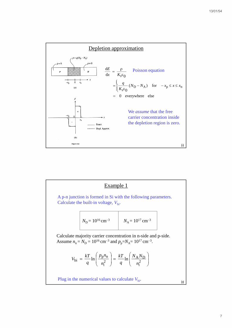
Example 1
A p-n junction is formed in Si with the following parameters. Calculate the built-in voltage, Vbi.
ND = 1016 cm–3 NA = 1017 cm–3
Calculate majority carrier concentration in n-side and p-side. Assume nn = ND = 1016 cm−3 and pp=NA= 1017 cm−3.
=
=
2i
DA2i
npbi lnln
n
NN
q
kT
n
np
q
kTV
Plug in the numerical values to calculate Vbi.

13/01/54
8
1515
Example 2
A pn junction is formed in Si with the following parameters. Calculate the built-in voltage, Vbi.
ND = 2 ×1016 cm-3 NA = 3 ×1017 cm-3
NA = 1016 cm-3 ND = 2 ×1017 cm-3
Calculate majority carrier concentration in n-side and p-side. nn=“effective ND” = 1016 cm-3. pp = “effective NA”=1017 cm–3.
=
=
2i
DA2i
npbi lnln
n
NN
q
kT
n
np
q
kTV
Plug in the numerical values to calculate Vbi.
Here NA and ND
are “effective” ornet values.
16

13/01/54
9
17
Chapter 5-2 Quantitative electrostatic relationships
We make the analysis in 1 dimension, even though actual diode as shown may not be a one-dimensional system. This makes the analysis simple. The metallurgical junction is located at x = 0.
18
Quantitative analysis: Electric field E
pn
nD
pA
0s
;0
0
0
whered
d
xxxx
xxNq
xxNq
Kx
−<>=
<<ε
=
<<−ε
−=
ε=εερ
=E
p nNA
ND
−xp 0 xn
W
Emax = − q NA xp/ε= − q ND xn/ε
( )
np
nnD
ppA
0
0)(
)(
xx;xx
xxxxqN
oxxxxqN
x
>−<=
≤≤−ε
−=
≤≤−+ε
−=E

13/01/54
10
19
Relationship between xn and xp
Emax = − q NA xp / ε = − q ND xn / ε
NA xp = ND xn
Net charge on p-side = Net charge on n-side
Depletion layer width: W = xn + xp
DA
Dp
A
An
D NN
NWx
NN
NWx
+=
+=
If NA >> ND, then W ≈ xn and if NA << ND, then W ≈ xp
20
Built-in voltage: Vbi
dxxVdx
dV x
x)(or n
pbi EE ∫ −
−=−=
Vbi = − {area under E versus x curve}
= − (1/2) {W (-q ND xn / ε) }
= (q / 2ε) ND xn W
DA
An
DA
DA since22
1
NN
NWxW
NN
NNq
+=
+ε=
21
biDA
DA2/
VNN
NN
qW
+ε=

13/01/54
11
21
Quantitative analysis: Electrostatic potential
nnD
bi
ppA
p
nnD
ppA
02)(2
02(2
)(
zerotosetatpotentialreferencethewith
0)(
0d
d
xxxxqN
V
xxxxqN
xV
xx
xxxxqN
xx)xx(qN
x
V
)
≤≤−ε
−=
≤≤−+ε
=
−=
≤≤−ε
=
≤≤−+ε
=
V
x
Vbi
22
Step junction with VA ≠ 0
The equation for W is similar to the earlier equation except thatVbi is replaced by Vbi − VA; (VA is restricted to VA < Vbi).
21
AbiDA
DA )(2
/
VVNN
NN
qW
−
+ε=

13/01/54
12
23
Effects of forward and reverse bias
24
PN-junction energy-band diagrams

13/01/54
13
26
PN-junction diode: I-V characteristics
Topics:
PN Junction under bias (qualitative discussion)Ideal diode equationDeviations from the ideal diodeCharge-control approach

13/01/54
14
27
PN junction under various bias conditions
p n
VA = 0 VA > 0 VA < 0
Hole diffusion current
Hole drift current
Electron diffusion current
Electron drift current
p n
Hole diffusion current Hole diffusion current
Hole drift current Hole drift current
Electron diffusion current Electron diffusion current
Electron drift current Electron drift current
EE E
28
Band diagram and carrier flow under bias

13/01/54
15
29
Band diagram and carrier flow under bias
30
Effect of bias on diffusion current
When the diode forward-bias-voltage is increased, the barrier for electron and hole diffusion current decreases linearly. See the band diagram.
Since the carrier concentration decreases exponentially with energyin both bands, diffusion current increases exponentially as the barrier is reduced.
As the reverse-bias-voltage is increased, the diffusion current decreases rapidly to zero, since the fall-off in current is exponential.

13/01/54
16
31
Effect of bias on drift current
When the reverse-bias-voltage is increased, the net electric field increases, but drift current does notchange.In this case, drift current is limited NOT by HOW FASTcarriers are swept across the depletion layer, but rather HOW OFTEN.
The number of carriers drifting across the depletion layer is small because the number of minority carriers that diffuse towards the edge of the depletion layer is small.
To a first approximation, the drift current does not changewith the applied voltage.
32
Effect of bias on the “net” current
|Idrift| does not change with applied voltage, VA
|Idiff| varies exponentially with applied voltage (Why?) |Idiff| = I0
exp (VA/Vref) where I0 and Vref are constants.
Net current = Idiff – Idrift
At equilibrium, VA = 0; Net current = 0
| Idiff |VA = 0 = | Idrift |VA = 0 = I0
At any applied voltage, VA,
since Idrift= I0 at any voltage.
)1(ee ref
A
ref
A
0drift0 −=−= V
V
V
V
IIII

13/01/54
17
33
Quantitative solution
Assumptions which must hold
– The diode is being operated under steady state conditions
– A non-degenerately doped step junction models the doping profile
– The diode is one-dimensional
– Low-level injection (conditions) prevail in the quasi-neutral regions
– There are no processes other than drift, diffusion, and thermal recombination-generation taking place inside the diode, GL=0
– The electron and hole currents are constant throughout the depletion region
34
Majority and minority carrier concentration under equilibrium
p-side n-sidepp0
np0
nn0
pn0
EEEE
Hole diffusion current
Electron diffusion current
Hole drift current
Electron drift current
Subscript “0” refers to equilibrium conditions
-xp xn

13/01/54
18
35
Relationship between carrier concentration and Vbi
( ) ( ) side-niFside-pFibi EEEEV −+−=
+
=
i
n0
i
p0lnln
n
n
q
kT
n
p
q
kT
36
Relationship between carrier concentration and Vbi
=
2i
n0p0bi ln
n
np
q
kTV
=
n0
p0lnp
p
q
kTn0
n0
2i p
n
n=because
Therefore, kT
qV
p
p bi
e0n
0p = and kT
qV
n
nbi
e0p
0n =
side-ponconc.electron
side-nonconc.electrone
side-nonconc.hole
side-ponconc.holebi
== kT
qV
Strictly, these concentrations are at the depletion layer edge

13/01/54
19
37
Majority and minority carrier concentration under bias
When an external voltage is applied, the minority carrier concentration at the edge of the depletion layer will change. If a forward voltage (VA=positive) is applied, the barrier will be lower and carrier injection (diffusion part) will increase. The minority carrier concentration at the edge of the depletion layer will increase.
If a reverse voltage (VA = negative) is applied, the barrier for carrier injection (diffusion part) will increase, and the minority carrier concentration at the edge of the depletion layer will decrease.
At VA = 0, the carrier injection and the drift of minority carriers cancel each other such that an equilibrium conc. is maintained.
If “low-level-injection” condition is assumed, then the majority carrier concentration will not change under any of the above conditions.
38
Relationship between carrier concentration and VA
( )kT
VVq
p
p Abi
en
p−
=since (Vbi – VA) is the net voltage (or barrier) when a forwarded voltage is applied.
At low-level injection: pp= pp0; Recall that
then
kT
qV
kT
qV
kT
qV
kT
VVq
ppppAAbiAbi
eeee n0p0
)(
p0n ===
−−−
kT
qV
p
p bi
en0
p0 =
kT
qV
p
pA
e0n
n = kT
qV
n
n A
ep0
p =

13/01/54
20
39
Minority carrier concentration profile under bias
x'x''
pe)0()( nnL
'x
p'xp−
∆=∆ne)0()( ppL
''x
n''xn−
∆=∆
pn = pn0 + ∆pn(x')np= np0 +∆np(x'')
∆pn(0)∆np(0)
pn0np0
+ VA −
40
Relationship between applied voltage and excess minority carrier concentration
( ) n0nn 0)0( ppp −=∆
kT
qV
p
pA
e)0(
n0
n =
kT
qV
ppA
e)0( n0n =
)1(A
n0 −= kT
qV
ep
kT
qV
n
n A
e)0(
p0
p =
kT
qV
nnA
e)0( p0p =
( ) p0pp 0)0( nnn −=∆
)1(eA
p0 −= kT
qV
n

13/01/54
21
41
Current-Voltage Characteristics
Depletion region, energy band diagram and carrier distribution.
(a) Forward bias. (b) Reverse bias.
42

13/01/54
22
43
Carrier injection under forward bias
Last class, we established the excess minority carrier concentration profile under biased conditions.
The excess minority carrier concentration at the edge of the depletion layerwill increase under forward biased condition. The minimum carrier concentration decreases exponentially with distance from the depletion layer edge.
pn e)0()(e)0()( nnppL
'x
L
''x
p'xpn''xn−−
∆=∆∆=∆
44
Carrier injection under forward bias
At equilibrium, # of holes diffusingto n-sideequals # of holes drifting from n-side. When we apply external forward voltage, VA, holes diffusing (injection) to n-side from p-side increases exponentially. This increases the hole concentration at the edge of the depletion layer on n-side.
kT
qV
pxpA
e)( n0nn =
n0nnnn )()( pxpxp −=∆ )1(eA
n0 −= kT
qV
p
)1(e)(A
p0pp −=−∆ kT
qV
nxn
Similarly,

13/01/54
23
45
Minority carrier concentration profile under bias
x'x''
pe)0()( nnL
'x
p'xp−
∆=∆ne)0()( ppL
''x
n''xn−
∆=∆
pn = pn0 + ∆pn(x')np= np0 + ∆np(x'')
∆pn(0)∆np(0)
np0
+ VA −
pn0
' nx x x= −'' ( )px x x= − +
46
Carrier injection under forward bias (continued)
Change of axes to x' and x'' (see graph)
)1(e(0)A
n0n −=∆ kT
qV
pp
x' axis
pA
p
e)1(e
e(0))(
no
nn
L
'x
kT
qV
L
'x
p
p'xp
−
−
−=
∆=∆
)1()0(A
p0p −=∆ kT
qV
enn
x'' axis
n
A
n
e)1(e
e)0()(
p0
pp
L
"x
kT
qV
L
''x
n
n"xn
−
−
−=
∆=∆

13/01/54
24
47
Current-Voltage Characteristics
Since we assume that no current is generated within the depletion region, all currents come from the neutral regions. Also, there is no E field inside the neutral regions.
In the neutral n-region, the steady-state continuity equation can be expressed as
20
20n n n
p p
d p p p
dx D τ−
− =
48
Current-Voltage Characteristics
The solution of the previous equation with the boundary conditions of
and pn (x’ = ∞)= pn0
gives
where Lp is the diffusion length of holes in the n-region =
p pD τ
/0 0(0) ( 1)AqV kT
n n np p p e− = −
'/ '//0 0( 1) (0)p pA
x L x LqV kTn n n np p p e e p e− −− = − = ∆
p pD τ

13/01/54
25
49
Current-Voltage Characteristics
Similarly for the neutral p-region:
where Ln is the diffusion length of electrons in the p-region =
''/ ''//0 0( 1) (0)n nA x L x LqV kT
p p p pn n n e e n e− −− = − = ∆
n nD τ
50
General current and minority carrier diffusion equations
x
pqDqpxJ
d
d)( ppp −µ= E
x
nqDqnxJ
d
d)( nnn +µ= E
Lp
2
2
p Gp
x
pD
t
p+
τ∆
−∂
∆∂=
∂∆∂
Ln
2
2
n Gn
x
nD
t
n+
τ∆
−∂
∆∂=
∂∆∂
Simplified equations
x
pqDxJ
d
d)( pp −=
p2
2
p0τ∆
−∂
∆∂=
p
x
pD

13/01/54
26
51
Current equations applied to a diode
"x
nqD"xJ
d
d)( nn
∆=
'x
pqD'xJ
d
d)( pp
∆−=
Find Jn and Jp at the edge of the depletion layer and add them to get the total current.
Assumption: No generation or recombination inside the depletion layer.
x'' x'
52
Current equations applied to a diode
npp d
dp
'xqDJ −=
( ) e0 pnp
p L/'xpL
Dq −∆
+=
( )[ ]e0d
dp
nn0pL/'xpp
'xqD −∆+−=
( ) )1(e0)0(A
n0p
pn
p
pp −
=∆
== kT
qV
pL
qDp
L
qD'xJ
Therefore,

13/01/54
27
53
Diode current equations
)1()0(A
p0n
nn −
−== kT
qV
enL
qD''xJSimilarly,
And total current equals,
Ap n
n0 p0p n
(e 1)qV
kTqD qD
J p nL L
= + −
)1(A
0 −= kT
qV
eJJ
Current due to electrons will be along positive x' direction.
Shockley equation,
p n0 n0 p0
p ns
qD qDJ J p n
L L
= = + where
Ideal diode equation
54
Forward and reverse bias characteristics
J
)1(eA
0 −= kT
qV
JJ
Large forward bias (VA >> kT/q):
kT
qV
JJA
e0=
Large reverse bias (VA << –kT/q):
0JJ −=

13/01/54
28
55
Ideal current-voltage characteristics.
(a) Cartesian plot.
(b) Semilog plot.
56
Current-Voltage Characteristics
Injected minority carrier distribution and electron and hole currents.
(a) Forward bias.
(b) Reverse bias.
The figure illustrates idealized currents. For practical devices, the currents are not constant across the space charge layer.

13/01/54
29
57
Current-Voltage Characteristics
The figure shows that the injected minority carriers recombine with the majority carriers as they move away from the boundaries.
The hole and electron diffusion current will decay exponentially in the n-region with diffusion length Lp and p-region with diffusion length Ln, respectively.
( ) pp '/n
p
( ') 0 e x Lp
DJ x q p
L−
= + ∆
( ') ( ')n pJ x J J x= −
58
Current-Voltage Characteristics
Ex. Calculate the ideal reverse saturation current in a Si p-n junction diode with a cross-section area of 2 x 10⁻⁴
cm2. The parameters of the diode are
NA = 5 x 106 cm-3, ND = 1016 cm-3, ni = 9.65 x 109 cm-3, Dn =
21 cm2/s, Dp = 10 cm2/s, and τp = τn = 5 x 10⁻⁷ s.

13/01/54
30
59
Current-Voltage Characteristics
Soln From (19) and p n nL D τ=
( )
0 0
2
219 916 7 16 7
12 2
-4 2
-4 12
1 1
1 10 1 211.6 10 9.65 10
10 5 10 5 10 5 10
8.58 10 A/cm
From the cross-section area A = 2 10 cm , we have
2 10 8.58 10 1.7
p n n ps
p n
p ni
D p A n
s s
eD p eD nJ
L L
D Den
N N
I A J
τ τ
−− −
−
−
= +
= +
= × × × +
× × ×
= ×
×
= × = × × × = 152 10 A−×
60
Figure 6.3 is a dimensioned plot of the steady state carrier concentration inside a pn junction diode maintained at room temperature.
a. Is the diode forward or reverse biased? Explain
b. Determine the applied voltage, VA
c. Determine the hole diffusion length, Lp
Example 1

13/01/54
31
61
62
Small-signal admittance
Reverse bias junction or depletion layer capacitance
Forward bias diffusion or charge storage capacitance
Forward and reverse bias conductance.
We will study the small signal response of the pn junction diode. A small ac signal (va) is superimposed on the dc bias. This results in ac current (i). Then, admittance Y is given by:
Y= i / va = G + jωC
Specifically, the following parameters will be studied.

13/01/54
32
63
Capacitance measurements
I = dc
i = ac
Y= admittance
CjGv
iω+==
ac
Model for a diode under ac
i and va depends on theapplied dc bias
64
Reverse bias junction capacitance
pn junction under reverse bias behaves like a capacitor.
Such capacitors are used in ICs as voltage-controlled capacitors.
Depletion layer width under small ac superimposed on DC bias voltage.
Looks similar to a parallel plate capacitor.
W
AC Si
jε
=where W is the depletion layer width under dc bias.

13/01/54
33
65
Reverse bias junction capacitance
( )21
AbiDA
DASi2/
VVNN
NN
qW
−
+ε=
( )21
AbiB
Si2/
VVqN
−
ε=
( )
21
Abi
BSiJ 2
/
VV
qNA
W
AC
−ε
=ε
=
For pn junction
For p+n or pn+ junction where NB is the doping on the lightly doped side
For asymmetrically doped junction
CJ increases with NB1/2
CJ decreases with applied reverse bias
66
whereas, the depletion layer capacitance in a case of linearly graded junction can be expressed by
1/32
2 [F/cm ]12( )
si sij
bi A
eaC
W V V
ε ε = = −

13/01/54
34
Depletion Capacitance
Ex. For a silicon one-sided abrupt junction with NA = 2 x 10¹⁹
cm-3 and ND = 8 x 1015 cm-3, calculate the junction capacitance at zero bias and reversed bias of 4 V.
Depletion Capacitance
Soln( )
( ) ( )
19 15
29
14
19 150
8 2j 0
0
14
19 154
2 10 8 100.0259ln 0.906 V
9.65 10
2 2 11.9 8.85 10 0.906W
1.6 10 8 10
0.386 µm
C 2.728 10 F/cmW
2 2 11.9 8.85 10 0.906 4W
1.6 10 8 10
0.899
bi
s biV
D
s
VV
s bi
VD
V
V
eN
V V
eN
ε
ε
ε
−
−=
−
==
−
−=−
× × ×= =
×
× × × ×=
× × ×
=
= = ×
− × × × × +=
× × ×
=
≃
≃
8 2j 4
4
µm
C 1.172 10 F/cmW
s
VV
ε −
=−=−
= = ×

13/01/54
35
69
Parameter extraction/profiling
C-V data from a pn junction is routinely used to determine the doping profile on the lightly doped side of the junction.
( )
21
Abi
BSiJ 2
/
VV
qNA
W
AC
−
ε=
ε=
( )AbiSiB
22J
21VV
qNAC−
ε=
If the doping on the lightly doped side is uniform, a plot of 1/CJ
2 versus VA should be a straight line with a slope inversely proportional to NB
and an extrapolated 1/CJ2 = 0
intercept equal to Vbi.
1/Cj2
[F–2 ]
VA [Volts]
Intercept = Vbi
0
1
2
0–5–10
2SiB
2Slope
AqN ε=
70
Forward bias diffusion capacitance, CD
CD is also called the charge storage capacitance. Minority carrier charge fluctuation results in diffusion capacitance. Both CJ and CD
are always present, but for forward biased case, CD becomes dominant.
origin of diffusioncapacitance.
x
p n
np0pn0
kT
qV
pqALkT
qVp
L
DqAIQ
A
e1exp n0pA
n0p
pppp ≈
−
τ=τ=
pn0pp
D expd
dτ=
== IkT
q
kT
qVpqAL
kT
q
V
QC A
For a p+n junction, I = Qp/τp where Qp is total excess charge in n-side

13/01/54
36
71
Forward bias conductance
IkT
q
VL
pqAD
V
IG kT
qV
=
==
A
ed
d
d
d
p
n0pD
IkT
qG =D pD τ= I
kT
qC
1p <<ωτ
Assumes
Complicated at higher frequencies.
CJ
CD
GD
RsEquivalent circuit for a diode
VApplied = VA
VJ
72
Example
Consider a p+n junction forward biased such that the forwardcurrent is 1 mA. Assume the lifetime of holes is 10–7 s. Calculatethe diffusion capacitance and the diffusion resistance.

13/01/54
37
73
74
Deviations from the ideal
Mostly qualitative understanding of non-ideal behavior of the diodes:
Reverse-bias breakdown
– Avalanching
– Zener process
The R-G current
If VA → Vbi, then high-current phenomena result
– Series current
– High-level injection

13/01/54
38
75
I-V Characteristic of commercial Si diode at 300K
76
Detailed I-V plots of commercial Si diode at 300K
Series resistance effect
Ideal behavior
G-R part
G-R partBreakdown
High level injection

13/01/54
39
77
Reverse-bias breakdown
A large reverse current flows when the voltage exceeds certain value. Not destructive unless power dissipationcauses excessive heating.
For a p+n or pn+ diode: VBR ∝ ∝ ∝ ∝ NB–1
where VBR is the breakdown voltage and NB is the (bulk) doping on the lightly doped side.
Two processes:Avalanching:dominant process in lightly doped diodes.Zener process:more important in heavily doped diodes.
78
AvalanchingCarrier multiplication due to impact ionization occurs at high reverse voltage, when the electric field reaches a critical value, EEEECR. These additional carriers are swept across the depletion layer due the high electric field.
P N
VA<< 0
E -field
The increase in current associated with the carrier multiplication is modeled by introducing a multiplication factor, M (= I / I0) and the multiplication factor can be empirically fit to an equation
m
V
|V|M
−
=
BR
A1
1
where m is between 3 and 6.

13/01/54
40
79
Carrier activity within a reversed-biased diode
Carrier multiplication due to impact ionization
80
Avalanching
( ) 21
AbiDA
DA
Si
nSi
D
2
)0(
−
+ε−=
ε−==
VVNN
NNq
xqN
xE
Emax = − q NA xp/ε= − q ND xn/ε
E
x
p n
Breakdown occurs when E (0) = ECR; and when (Vbi – VA ) → ( Vbi – VBR) ≈ VBR
Eq. 5.30a
DA
DABR
21
BRDA
DA
SiCR or
2
NN
NNVV
NN
NNq/
+∝
+ε=E
For asymmetrically doped junctions:(where NB is the (bulk) doping on lightly doped side) B
BR1
NV ∝

13/01/54
41
81
Zener process
Tunneling in a reverse biased diode - occurs in heavily doped diodes
82
The R-G current: reverse-bias case
In an ideal diode, the reverse current is I0 = q A [Dp pn/Lp+ Dn np/Ln]and this current is a constant. The ideal diode equation was derivedassuming no generation of carriers in the depletion layer. In an actual device, the thermal generation of carriers in the depletion layer should be taken into consideration.
The current due to thermal generation (IR-G) increases with thevolume of the depletion layer (or W).
Volume (or W) increases with the applied reverse bias. So, IR-G
increases as reverse voltage is increased.
WnAq
I0
iG-R 2τ
−=
Detailed analysis shows that IR-G for reverse bias can be written as:
where τ0 = f(τp + τn) ≈ (τp + τn) / 2

13/01/54
42
83
The R-G current: forward-bias case
Under forward bias, some of the injected carriers may recombine while crossing the depletion layer. This was neglected in the analysis of “ideal” diode.Detailed analysis shows that:
)1(e20G-R
A
−= kT
qV'II ... in the forward bias case.
Total forward current : I = Idiff + IR-G where Idiff is the current (called diffusion current) described by the “ideal” diode equation.
Idiff increases more more rapidly with bias compared to IR-G. So, Idiff
dominates at higher forward voltage.
+=
−=
D
2i
p
p
A
2i
n
n00diff where1e
A
N
n
L
D
N
n
L
DqAIII kT
qV
84
Relative values of IR-G and Idiff
In Si, q A ni W / 2τ >> I0 and IR-G current dominates at reverse bias and at small forward bias. Since IR-G ∝ W, the reverse current never saturates, but continually increases with reverse bias.
Since Idiff ∝ ni2 and IR-G ∝ ni, the relative values of Idiff and IR-G
varies from semiconductor to semiconductor. In Si and GaAs at 300 K, q A ni W / (2τ) >> I0 whereas in Ge, I0 >> q A ni W / (2τ). So, Ge more closely follows ideal diode equation, I = I0 [exp (q VA/ kT) – 1] at 300K.
Since Idiff ∝ ni2 and IR-G ∝ ni, Idiff increases at a faster rate with
increasing temperature. So, even Si follows the ideal diodeequation, I = I0 [exp (q VA / kT) – 1] at higher temperature.

13/01/54
43
85
VA → Vbi high-current phenomena
As VA approaches Vbi, a large current flows. Two phenomena become important: series resistance effect and high-level injection.
Series resistance effect:
Some voltage drops in the “quasi-neutral” and ohmic-contact region reducing the actual voltage drop across the junction.
biA
)(
000 whenee1esAjj
VVIIII kT
IRVq
kT
qV
kT
qV
→=≈
−=
−
Here, Vj is the actual voltage across the junction, and VA is theapplied voltage. Some of the applied voltage is wasted, so thatlarger applied voltage is necessary to achieve the same level ofcurrent compared to the ideal.
86
Identification and determination of diode series resistance

13/01/54
44
87
High level injection
When the forward voltage is within a few tenths of a volt below Vbi , high current flows, and the low-level injection assumptionbegins to fail. High level injection phenomena should be consideredin deriving I-V characteristics. More detailed analysis shows thatthe current increases roughly as exp [q VA / (2kT)] when VA → Vbi