Picosecond Switching Measurements Of A Josephson Tunnel Junction BY
90
- Picosecond Switching Measurements Of A Josephson Tunnel Junction BY Douglas R. Dykaar Department Of Electrical Engineering Advisor: T.Y. Hsiang Ph.D. Thesis Submitted in partial fulfillment of the requirements for the degree DOCTOR OF PHILOSOPHY May 1987
Transcript of Picosecond Switching Measurements Of A Josephson Tunnel Junction BY
- Picosecond Switching Measurements
Of A Josephson Tunnel Junction
BY
Douglas R. Dykaar
Department Of Electrical Engineering
Advisor: T.Y. Hsiang
Ph.D. Thesis
Submitted in partial fulfillment
of the
requirements for the degree
DOCTOR OF PHILOSOPHY
May 1987


Table Of Contents
Curriculum Vitae
Acknowledgment
Abstract
1. Preamble
2. Historical Notes: Superconducting Electronics to Fast Lasers
3. Josephson Junction Theory
A. Tunneling Theory
B. Tunnel Junction Theory
C. Circuit and Pendulum Models
4. Early Experiments
A. Purpose
B. Pb Junction Fabrication
C. Single Shot Technique
i) Pulse Generation: Photoconductive Switch
ii) Signal Measurement Technique
iii) Results
D. Flux Flow Theory
E. Discussion: Limitations of Theory
5. Electro-optic Sampling: Overview of Experimental Technique
A. Electro-optic Sampling Theory
i) CPM Laser
ii) Pockels Effect
B. Microvolt Implementation of Electro-optic Sampling

5. Electro-op tic Sampling (continued)
C. Cryogenic Adaptation of Electmoptic Sampling
D. Femtosecond System Calibration
6. Cryogenic Experimental Results
A. Coplanar Transmission Line Design
B. Sample Design
C. Probe Design
D. Tunnel Junction Experiments I (Quasi-Static)
E. Indirect Measurements (I-V Technique)
F. Tunnel Junction Experiments II
G. Indirect Measurements (Chaos)
7. Numerical Simulations
A. Junction Transient Response Simulations (JSPICE)
B. Introduction To Chaos
C. Numerical I-V Simulations
8. Work in Progress
A. Alternative Sampling Geometries
B. Dispersion on Superconducting Transmission Lines
C. Spectroscopy in Superfluid Helium
D. Contactless Infrared Sampling
E. Alternatives to Superconductivity: The PBT
9. Conclusion
10. Appendix
1 1. References

Curriculum Vitae
Douglas Raymond Dykaar was born on July 19, 1957 in ~ e w - ~ o r k City's
Mount Sinai Hospital. At the time his parents resided in the Bronx, although this was
mercifully exchanged for the borough of Queens after only two months and finally
Nassau county.
He attended Brown University from 1975 until 1979 and received the Sc.B.
degree in Engineering. In the fall of 1979 he entered the Ph.D. program in Electrical
Engineering at the University of Rochester, receiving the M.S. degree in 1981.
During his first year of study, Mr. Dykaar was a Fellow of the Department of
Electrical Engineering. Since that time he has been a Research Assistant at both the
Department of Electrical Engineering and the Laboratory for Laser Energetics, as well
as one year (1985) as an IBM hedoctoral Fellow.
Mr. Dykaar's research in Electrical Engineering was performed under the
guidance of Professor Thomas Y. Hsiang.
Mr. Dykaar is a member of the IEEE, PCA and APS.

Acknowledgment
It is a great relief to be able to acknowledge the tremendous help a a patience of
my advisor Professor Thomas Y. Hsiang, as well as Professor Gerard A. Mourou. I
am also indebted to Charles V. Stancampiano, who guided me through the treacherous
and frightening transition from undergraduate to graduate student and finally to
Graduate Student. In addition, some of the later work reported here was done with the
help of Roman Sobolewski, whose ability to bum the midnight oil with complete
abandon made possible the survival of many long experiments which were followed
by the new day's dawn.
Any student who has worked at the Laboratory for Laser Energetics ("Laser
Lab") has come to know the critical mass of intelligence represented by the other
members of the ultrafast group. A special thanks goes to all those members of the
ultrafast lane (both past and present) for their help and cooperation (despite my poor
French language skills).
I am also thankful for the help I received from the Electrical Engineering
department faculty and staff, as well as the financial support I received from the
Department of Electrical Engineering, the Laboratory for Laser Energetics and IBM.
Finally, I am thankful that my parents made this possible, in that they made me
possible to be where I now find myself.

Abstract
The advent of short pulse lasers has made possible the study of many new
high-speed phenomena. This work is a study of superconducting Josephson tunnel
junctions, which are excited by laser-generated current pulses.
These experiments make use of both pico- and subpicosecond lasers in
conjunction with silicon, gallium arsenide and indium phosphide photoconductive
switches. The combination of laser pulse and photoconductive switch is used to create
current pulses with fast rise time, adjustable amplitude, and in some cases, adjustable
width.
The current pulses are then used as excitations for Josephson tunnel junctions,
recognized as being among the fastest devices known. Tunnel junctions were
fabricated at the University of Rochester, as well as at the National Bureau of
Standards in Boulder, Colorado.
To measure the time domain response of these devices directly, a cryogenic
electro-optic sampler was implemented with an unprecedented time resolution. An
electrical transient propagated on a transmission line, with a rise time of 360 fs - a
record to this date - has been measured. In addition, a new detection scheme was
implemented which allowed measurements approaching the shot-noise limit.
These advances in technology by the author were the key to being able to study
the dynamics of Josephson junction behavior. Once this system was perfected, it was
then possible to study the junction dynamics on a picosecond time scale.
The response of these junctions has been studied both directly in the time
domain, and indirectly by studying the changes in the junction I-V curve caused by the
high-speed excitation.

For the first time, measurements were made on a single Josephson junction
which cannot be explained using a simple quasi-static model. That is, a summation of -
bias and applied pulse current did not yield the critical value. More surprising perhaps,
than the discovery of an upper limit on junction performance, was the successful
modeling of these measurements using the standard CRSJ model.
In addition, chaos has been directly observed in the I-V characteristics of these
devices due to the periodic kicks that these current pulses represent. This is the first
direct observation of chaos in a periodically kicked Josephson junction. As with the
time domain study, this phenomenon was also simulated remarkably well using simple
dynamical models to represent the junction. Insights into both the origins, as well as
the fully developed chaotic behavior were gained from the simulations. These
simulations matched the experimentally measured values of the switching threshold to
a surprising degree.
The results of these experiments led the author to the development of the concept
of a critical pulse charge, rather than a critical current, as the measure of the junction
switching threshold. This concept is fundamentally different from the previous
measure of the junction switching threshold. The concept was further refined by the
author to include the concept of a critical rise time. For excitations of a given width and
amplitude, those with a faster onset than this critical rise time, will result in chaotic
behavior. These new concepts in junction characterization were the direct result of
these experimen ts.
The techniques developed by the author for these studies have also been utilized
in other experiments, such as signal propagation studies on superconducting and
normal transmission lines, and characterization of other two terminal devices, such as
the resonant tunneling diode and superconducting bridge.

1 Preamble
1 Preamble
- This thesis is as much a history of the development of ultrafast cryogenics as it
is a study of superconducting phenomena. The organization reflects this theme: after
some introductory and background chapters, the results are presented in essentially
chronological order.
A brief historical outline is presented in Chap. 2, followed by Josephson
junction theory in Chap. 3. This chapter not only presents the basic operating
characteristics of Josephson junctions, but the junction analogs, which are critical to
modeling these devices as well as the key to understanding their behavior.
Chapter 4 presents the first experimental results of a Josephson junction, driven
by a laser-generated current pulse. These early results are modeled using a flux-flow
theory presented at the end of the chapter.
Next, in Chap. 5, fast electro-optic sampling is summarized, including a
description of the high-speed laser used, the detection electronics and the basic
cryogenic techniques necessary for the experiments which follow.
These experiments are presented in Chap. 6. They include the design and
construction of both the transmission line structures as well as the probes used in the
experiments. Two sets of experimental results are presented: those in which the signal
source remained outside the dewar at room temperature, and the fully integrated
structure Finally, the results of the first observation of chaos in a periodically kicked
rotator are presented.
In Chap. 7 simulations of the experimental results are presented. These include
Junction simulations for both the transient case and I-V curves (chaos). The results of
these studies are compared with the experimental results of Chap. 6.

1 Preamble
Chapter 8 presents ongoing studies and includes some peripherally related work
done by the author as well as ongoing experimental work and suggestions for future
study. These include simulations of the signal propagation studies, as well as
simulations of the transmission line impedance at energy gap frequencies. Also
presented are experiments in infra-red electro-optic sampling and time domain studies
of a novel transistor developed at MIT's Lincoln Laboratory, the Permeable Base
Transistor.
This study concludes with an overall summary of the work and a final thought
on the immediate future of the field.

2. Historical Notes
2 Historical Notes: Superconducting Electronics to Fast Lasers
- Although the liquefaction of helium was achieved in 1907, it was not until
recently that the real potential of superconductivity has been realized [1],[2]. A
somewhat narrow view of the event time line is shown in Fig. 2.1. The events are
restricted to those which pertain to the development of the high-speed Josephson
junction as it is known today, along with the development of the high speed
characterization techniques which made time domain study of the Josephson junction
possible.
Those high speed techniques are all based on the laser, which was not
developed until the 1960s [3]. The first lasers were not high speed devices at all, being
driven by flashlamps as they were. The truly high speed lasers were the dye lasers,
developed in the 1970s at Bell Labs. These ring lasers had optical pulse widths on the
order of 100 fs, and were among the fastest laboratory events. As a tool for research,
however, they left much to be desired. This pulse was optical after all and the
phenomena of interest were electronic.
The bridge between the electrical and optical domains was made in 1982, when
an electro-optic Pockels cell was used to modulate a fast laser with a high speed
electrical signal used as the modulation signal [4]. The first results obtained with the
system were on the order of a few picoseconds @s), but as better modulators were
built, the system response dropped, and by 1984, the risetimes being measured were
on the order of 500 femtoseconds (fs) [5]. Once this resolution was achieved, this
technique was applied to such diverse problems as transistor characterization and
superconducting physics [6]. The best electronic sampling oscilloscopes are limited to
tens of picoseconds, even today.

2. Historical Notes
- Author is born, BCS and Cooper Papers
- Shapiro, Giaver Tunneling Papers
- Josephson Paper
- IBM Josephson Project Begins
- Author Graduates High School
- Author Matriculates at Rochester - Ring Laser, Superconducting Sampler Constructed
- Electro-optic Sampler Constructed - IBM Josephson Project Ends
- Author Constructs First Electmoptic Oyo-sampler - Author Measures 360 fs Risetime
Figure 2.1 Event time line

2. Historical Notes 5
Given the steady advances being made in the optical domain, it is unlikely that speeds
in the electronic domain will catch up in the near future. Although great strides are
being made in new electronic devices, the fastest optical pulse is now onF 8 fs [7].
Given the huge advantage in speed in the optical domain, it appears likely that
research in ultrafast phenomena will continue to require the use of the optical domain
for the foreseeable future.

3 Josephson Junction Theory
This chapter f rs t presents a short introduction to tunneling theory, which is
necessary to understand the behavior of tunnel junctions. Next, a brief "tour" of the - Josephson junction is given. Finally, two useful analogs for Josephson junctions are
presented: the pendulum and washboard. In thinking about junction responses for
various excitations, these models are extremely useful and will be referred to
frequently.
3A Tunneling Theory [8]
In classical physics, if a panicle with some energy, E, approaches a potential
barrier of "height" Vo , then the particle is reflected for E < VO , and transmitted for E
> Vo . However, in quantum physics, the same particle with E < VO , has a finite
probability of existing on the far side of the barrier.
Now consider a banier which is a small gap between two metals. Here, the
particle is an electron, particle energy is imparted via an applied voltage, and
transmitted electrons constitute a current. Fig. 3A. 1 shows a tunneling diagram for the
Normal metal - Insulator - Normal metal (NIN) case at T = 0. In the case of electrons ,
we also require for tunneling that the electron tunnels to an unoccupied state. As
shown in the figure, only electrons in metal 1, which are above the occupied states in
letal2, are available for tunneling.
By using Fermi's Golden Rule 191, one can express the current through the
ier as:
2x =Ti [MI 1 NI (E) N2(E + e ~ ) [f@) - f(E t ev)] d~

3 Josephson Junction Theory
Insulator
Figure 3A. 1 Normal-Insulator-Normal (NIN) Tunneling Schematic (T = 0).
where I M I ~ is the tunneling matrix element, i.e. the probability of a particular
tunneling event taking place, Ni(E) is the density of states at zero temperature
(constant), and so the integrand is the difference in the distributions of occupation. For
the Fermi distributions at zero temperature, this is just equal to one divided by the
applied voltage, eV. In that case Eq. (3A. 1) becomes:
This is just Ohm's law. The term lM12 was shown by Harrison [lo] to depend
exponentially on the barrier thickness, as is expected from quantum tunneling theory.
Next, let us return to Eq. (3A.1), but now consider the case of two
superconductors separated by a barrier (SIS). For a superconductor, as shown by
BCS [ l l ] , the density of states can be represented as in Fig. 3A.2, i.e.

3 Josephson Junction Theory
- where Nn(0) is the density of states for a normal metal at zero temperature, and
A is the energy gap parameter. The gap, A , is material dependent, and represents half
of the energy (see Fig. 3A.2) required to break a pair. Using this , one can construct a
tunneling diagram as in Fig. 3A.1 for the SIS case. For generality, consider the case
of two different superconductors, S1 and S2 , so that A1 ;t A 2 . As shown in Fig.
3A.3a, for no applied voltage there can be no tunneling, since there are no unoccupied
states available to tunnel to. When the applied voltage reaches a value of A1 - A2 as
shown in Fig. 3A.3b there will be a sharp increase in the current as shown in Fig.
3A.4. This is due to the thermally excited states in S 1 having an asymptotically large
number of states to tunnel to. However, as the applied voltage increases, the thermally
excited states in S1 will have fewer and fewer available states, which results in the
decrease in the current shown in Fig. 3A.4.
When the applied voltage reaches Al + A2 , the occupied sub-gap states will be
able to tunnel as shown in Fig. 3A.3c, and the current will again rise sharply as
shown in Fig. 3A.4.
Finally, consider the tunneling current in the low temperature and low voltage
regime. Here the Ferrni distribution of Eq. 3A.1 can be simplified:

3 Josephson Junction Theory
Thermal Excitations
Figure 3A.2 Superconducting density of states.
Figure 3A.3a Superconductor-Insulator-Superconductor (SIS) Tunneling Schematic.

3 Josephson Junction Theory
Figure 3A.3b SIS Tunneling Schematic continued.
v
Figure 3 A . 3 ~ SIS TunneEng Schematic continued.

3 Josephson Junction Theory
for E = eV < A and eV >> kT, then f(E) - e x a g ]
Figure 3A.4 Tunneling I-V characteristic, after Giaever [12].
Substituting Eq. (3A.5) in to Eq. (3A.1) one obtains:
The last term in the integral can be taken outside, since it has no E dependence, and so:
I - (3A.7)
for A > eV >> kT. This can be used as a measure of junction quality.

3 Josephson Junction Theory
3B Tunnel Junction Theory
- The basic element of superconducting electronics is the Josephson junction.
While there are several types currently capable of being fabricated, it is the tunnel
junction which is usually chosen for digital applications because of the similarity
between the fabrication of conventional semiconductor, and Josephson tunnel junction
circuitry [13].
A Josephson tunnel junction can be made by evaporating a stripe of metal onto
an insulating substrate, oxidizing it, and then evaporating another layer of metal across
the first. Two possible geometries are shown in Fig. 3B.1.
Oxide
(a) "Z" Stripe Junction (b) In Line Junction
Figure 3B.1 Tunnel Junction Geometries
If the metals can be made superconducting and the oxide is thin enough
(nanometers), and without holes, then the junction will (below the superconducting
transition temperature and without applied magnetic field) exhibit a dc current-voltage
characteristic as shown in Fig. 3B.2.
The curve can be divided into two distinct regimes: zero- and finite voltage. In
the zero voltage regime the current is carried solely by electron pair tunneling which is
described by the Josephson relations:

3 Josephson Junction Theory
(3B. la) -
(3B. 1 b)
where @ is the wave function phase difference between the two superconductors, Ic is
the maximum zero voltage current (or critical current), and e and fi are the usual
physical constants.
In the finite voltage regime the Josephson relations are still valid, but in addition
Figure 3B.2 Hysteretic tunnel junction I-V characteristic

3 Josephson Junction Theory
the junction exhibits quantum-mechanical tunneling. This is manifested by a very high
resistance for values of voltage less than the energy gap voltage, Vg. The resulting
current due to this quasiparticle tunneling can be calculated.
In order for the junction of Fig. 3B.2 to function as a latch, it must be
current-biased at some current Ib < Ic. Then if the current is pulsed to a value I > Ic, P
the junction will generally switch to the finite voltage state. Due to the hysteretic nature
of the junction , the voltage will persist even after the current pulse decays. Resetting
the latch requires reduction of the total current to zero.
An alternative method for switching a tunnel junction is the control line
technique shown in Fig. 3B.3. In this arrangement , a current-carrying control line
passes in the vicinity of a junction. The control current, Icon, induces a magnetic field
in the junction, BO, which is related to the phase difference, $, across the junction by :
A
where n is the unit normal directed from one electrode to the other and d' is the
effective oxide thickness.
For a rectangular junction with uniform current density, the dependence of the
Control Line I con
Oxide I I I
Figure 3B.3 Control line geometry
3 Josephson Junction Theory
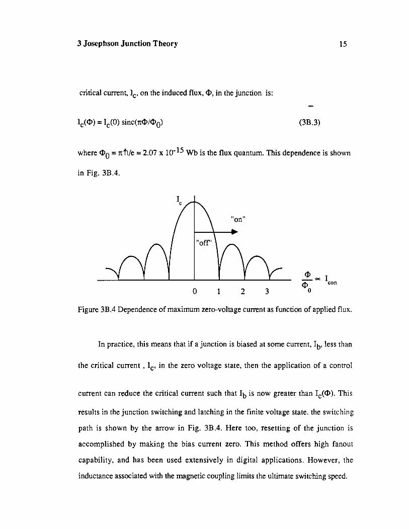
critical current, Ic, on the induced flux, 0, in the junction is: -
I,(@) = Ic(0) sin~(xQ>/Q>~) (3B. 3)
where OO = nfile = 2.07 x 10-l5 Wb is the flux quantum. This dependence is shown
in Fig. 3B.4.
Figure 3B.4 Dependence of maximum zero-voltage current as function of applied flux.
In practice, this means that if a junction is biased at some current, Ib, less than
the critical current , Ic, in the zero voltage state, then the application of a control
current can reduce the critical current such that Ib is now greater than Ic(Q>). This
results in the junction switching and latching in the finite voltage state. the switching
path is shown by the arrow in Fig. 3B.4. Here too, resetting of the junction is
accomplished by making the bias current zero. This method offers high fanout
capability, and has been used extensively in digital applications. However, the
inductance associated with the magnetic coupling limits the ultimate switching speed.

3 Josephson Junction Theory
In addition to applied magnetic fields, RF fields can be applied to a junction as
shown schematically in Fig. 3B.5. Here the junction is modeled as an ideal junction -
Figure 3B.5 Equivalent circuit for applied rf,
obeying Eqs. (3B.la) and (3B.lb), plus a shunt resistance, R, and capacitance, C.
For this circuit, the junction current, i.(t) can be expressed as : J 2eVs
i j t ) = I C z ( - 1 rJ[d sin [(m, - n o ~ t + Q0]
n=-m
where o. - ZVdC J-R and Q is a constant.
0
Equation (3B.5) is called the Josephson frequency - voltage relation and the
2e n fios quantity - is approximately 484 MHdpV. When w, = n y or Vdc =-
fi 2e
there will be current spikes in the junction dc I-V curve given by the dc part of
Eq. (3B.4). However, since real junctions are current biased (due to experimental
constraints), the curve actually shows a step like structure along the voltage direction.
The appearance of these Shapiro steps [14] under RF excitation and the modulation of
1, by an applied magnetic field are clear indications of the presence of the Josephson
effects.

3 Josephson Junction Theory
3C Circuit and Pendulum Models
- The standard CRSJ (Capacitively and Resistively Shunted Junction) equivalent
circuit for a real Josephson junction driven by a constant current, I, is shown in Fig.
Figure 3C. 1 Equivalent circuit for a real Josephson junction
In addition to an ideal element described by the Josephson relations ( Eqs. 3. la
and 3.1b), the circuit includes a junction capacitance, C, and a voltage dependent
conductance, G(V). The equation describing this circuit is the Stewart-McCumber
relation [15], [16]:
I = lCsin$ +VG(V) + CC ( 3 ~ . 1)
By substituting Eq. (3B.lb) into (3C.1) and taking G(V) as constant, the
voltage dependence can be eliminated:

3 Josephson Junction Theory
Compare this equation to that of a pendulum of mass m, swinging on a massless
rod of length 1, moving in a medium with damping c: - T = M ' ~ ; + C + + ~ ~ ~ sin+ (3c.3)
as shown in Fig. 3C.2. The total applied torque is T, and M is the moment of inertia of
the pendulum. A comparison of Eqs. (3C.2) and (3C.3) is given in table 3C.1. This
analog is useful for predicting junction behavior in many situations.
Figure 3C.2 Pendulum analog
Table 3C.1
Electrical: Eq. (3C.2) Mechanical Analog: Eq. (3C.3)
Phase Difference @
Voltage (= 6 )
Capacitance C
Conductance G
Critical Current I,
Source Current I
Angle @
Angular velocity 6 Moment of Inertia M
Damping c
Maximum Torque For No Rotation
Applied Torque T

3 Josephson Junction Theory
Potential Energy I
q 2x I- Phase -+
Figure 3C.3 Washboard analog
Another useful concept is the washboard analog. Here, as shown in Fig. 3C.3,
the junction is modeled as a ball of mass m, sitting in a "washboard" potential, which
is immersed in a viscous liquid. The comparison of this version of Eq. (3C.3) to
Eq. (3C.2) is given in Table 3C.2. Since the axes in Fig. 3C.3 are energy and phase,
this model is useful in considering current-phase relationships.
Table 3C.2
Elecmcal
Capacitance C
time constant l/(RC)
-I@ + Ic - Ic cos@
Washboard Analog [17]
Mass
Viscosity
Potential energy
Momentum

3 Josephson Junction Theory 20
Finally, it is possible to reformulate Eq. (3C.2) to make it more tractable for
numerical methods:
2e Ic where 0 r [T] t r normalized t h e and PC = [$][$I
Here the Stewart-McCumber parameter, PC , indicates the amount of hysteresis
in the junction , as shown in Fig. 3C.4. When PC = 0, no hysteresis appears, but for
PC >> 1, a large hysteretic region results.
It should be noted that all of the above analogies were formulated for a constant
Figure 3C.4 Normalized I-V characteristic.

3 Josephson Junction Theory
conductance. Real tunnel junctions exhibit the energy gap structure shown in Fig.
3B.2. However, for most purposes these models suffice for demonstrating general dc
behavior and functional relationships.

4 Single Shot Experiments
4A Purpose
The first set of experiments used a laser-driven photoconductive switch to excite
a Josephson tunnel junction. The laser available at the time was a low repetition rate,
relatively long-pulse system. However, since this was the first attempt to characterize a
junction using this technique, the experiment was designed to be as simple as possible:
large area tunnel junctions were used to insure that the junction response time would
be slow relative to the response of the system and the use of lead junctions allowed
junctions to be fabricated in house.
Due to the low repetition rate of the laser, the experiment was necessarily a
single shot one. However, by utilizing the hysteretic nature of the tunnel junction, a
successful switching event resulted in the latching of the junction into the voltage state.
The junction could then be reset by grounding the biasing supply between laser shots.
By adjusting the dc bias, the pulse width and the pulse height, the switching threshold
was mapped out.
This ability to set the bias, Ib , for each shot was an advantage of the single shot
system, as previously published simulations such as Ref. [17] had used current biased
junctions driven by a small overdrive.
The intent of these early experiments was to show the feasibility of using
laser-generated electrical pulses to measure the response of a Josephson junction.
The first section describes the fabrication and testing technique used to make
samples for these experiments. Next, the method of making short electrical pulses
from short optical pulses is presented. Section 4C(ii) presents details of the signal
measurement technique. The results of these experiments are described in section
4C(iii). Finally, the results are modeled using a theory based on flux flow, and in the
last section the limits of this theory are discussed.
4 Single Shot Experiments
4B Lead Junction Fabrication
Many superconducting metals have been used to construct tunnel junctions.
Since tin is easy to work with, it has been used in the past (both at University of
Rochester and elsewhere), for fabricating tunnel junctions [18],[19]. However, the
transition (or critical) temperature of tin, i.e. the temperature at which it becomes
superconducting, is 3.7 K, which is less than the boiling point of liquid helium (4.2 K
at atmospheric pressure). To the experimenter, this means that the liquid helium must
be transferred from the storage dewar into an experimental dewar, which is then
pumped on with a vacuum pump. The process of transferring and pumping on liquid
helium is wasteful of both time and helium.
At the beginning of these experiments it was decided that it would be useful to
develop an alternative to the tin junction, which had not been fabricated at the
university for some time. Lead was chosen since its transition temperature of 7.2 K is
greater than the boiling temperature of liquid helium at atmospheric pressure. This
meant that a lead junction could be tested by merely placing it in the storage dewar and
observing its dc I-V characteristic. Unfortunately, developing a usable, high-quality
junction proved to be a difficult proposition. While lead junctions are easily fabricated
and have been used by others in the past, lead has other properties which make
sandwich-type junctions with thermally grown oxides especially susceptible to
mechanical failure. Specifically, as the lead films are grown on an insulating substrate,
there are large differences in the coefficients of thermal expansion. When the junction
is heated, cooled, or for that matter just left lying around for a few hours, the metal
film becomes stressed and distorts.
One mechanism which can relieve this stress is shown in Fig. 4.B 1. As shown,
"hillocks" have grown on the surface and unfortunately, through the thin oxide layer

4 Single Shot Exper-iments 2 3
which fomw the junctit~n. In aticiiriot~ to hillocks, t iny \vhiskr.rs can form. growing
I~~rpcntticul:~rly from meti31 surf:~ce. These too, arc capntllc of puricruring the c,xitlr=
1, i t yz~ . - . : ~ t r i i tvhiIi: rl!e): \.L..cri. not ~!xer.vcil ir-I {hi:!;;: cspi.1-i11>eni:i., ~l:(:v !>,\LC bct.12 sctfrl
otlicr ~I:(:)L~;>s 1201.
0nc.c [tie oxide i:; ~)~!nc~t i l~c.d, [!It. juric~iot~ \ \ ? i l l t)ct~;ivc a!: il'sl,or.t~-d 1y ;I srn;!ll .. . ,
siipt.rcor~ductirig t i t ~ k . A jut~ct inn shol-ted in this ?yay t7>it!i stii! eicl1iI7,it i t ~ I I I I : ~
zc~-o-voltn~c c~rr.~-cn[, bat r ~ > r t!ac to the J o s c ~ ~ l i s c ~ ~ r.fi;:ct. I;ii_:i:tc ..1,1;2. zliov::; a:? I-\!
curve j'c~t n lc;:(,i jr~irc~ion, \ v f ~ i c . l l nl\las :pl'o!l;lt~l:t. !;lior:~.~l 1-)y i.>tit: of 1113' ;~ t : i ) \ ;~ :
~ ~ ~ c c l ~ : t r ~ ~ s i r ~ s ,

1"ig. ;l,[j:F %:ti; LC:, dis~,!;:~y 111c rlc I-V curvct O F the jur:cticil. I;roi11 1!1c 1-tJ c111.v~ i l
is Ix)ssibir to g:i\!gi: t.11:. r;u;ility uf' thc* jt:ni.ticw.
f..e;rd jij~c:tions \,vcl.c f:~l,sic;ited 03 0.25!'1 x s..j.5C)!) s O . 0 1 0 i t l . sni~i!!!irc
scibstr,ntt.s.
4 Single Shot Experiments 26
E l e c t r i c a l C o n n e c t i o n s
" D i p s t i c k " P r o b e -
Liquid Hel ium S t o r a g e Dewar
I .--j--i--- I I
I
I I T r i a n g l e Wave
I I
I I I L,- ------J
7.
Scope r d
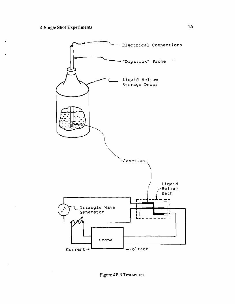
Figure 4B.3 Test set-up

4 Single Shot Experiments
Electric Heater
-Liquid Nitrogen
Metal t o be evaporated
Oxygen To Roughing Diffusion Pump Inlet Pump
Figure 4B.4 Vacuum system schematic.
4 Single Shot Experiments 28
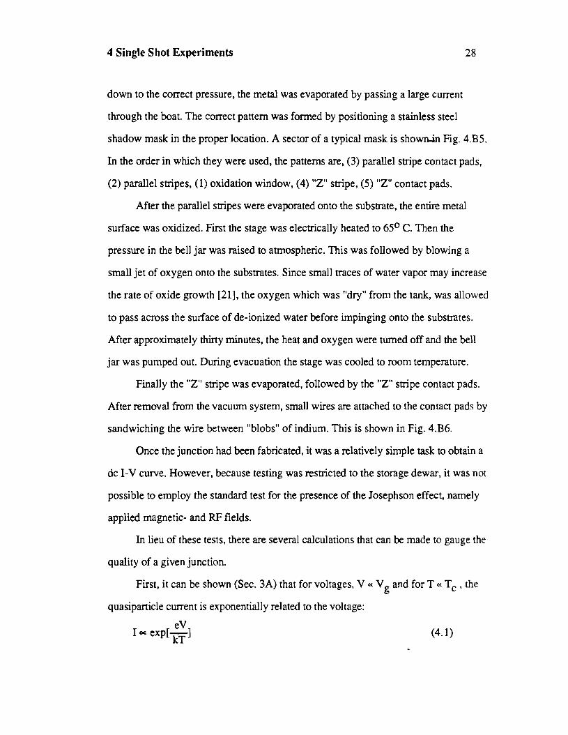
down to the correct pressure, the metal was evaporated by passing a large current
through the boat. The correct pattern was formed by positioning a stainless steel
shadow mask in the proper location. A sector of a typical mask is s h o d Fig. 4.B5.
In the order in which they were used, the patterns are, (3) parallel stripe contact pads,
(2) parallel stripes, (1) oxidation window, (4) "Z" stripe, (5) "Z" contact pads.
After the parallel stripes were evaporated onto the substrate, the entire metal
surface was oxidized. First the stage was electrically heated to 65O C. Then the
pressure in the bell jar was raised to atmospheric. This was followed by blowing a
small jet of oxygen onto the substrates. Since small traces of water vapor may increase
the rate of oxide growth [21], the oxygen which was "dry" from the tank, was allowed
to pass across the surface of de-ionized water before impinging onto the substrates.
After approximately thirty minutes, the heat and oxygen were turned off and the bell
jar was pumped out. During evacuation the stage was cooled to room temperature.
Finally the "2" stripe was evaporated, followed by the "Z" stripe contact pads.
After removal from the vacuum system, small wires are attached to the contact pads by
sandwiching the wire between "blobs" of indium. This is shown in Fig. 4.B6.
Once the junction had been fabricated, it was a relatively simple task to obtain a
dc I-V curve. However, because testing was restricted to the storage dewar, it was not
possible to employ the standard test for the presence of the Josephson effect, namely
applied magnetic- and RF fields.
In lieu of these tests, there are several calculations that can be made to gauge the
quality of a given junction.
First, it can be shown (Sec. 3A) that for voltages, V << V and for T << Tc , the g quasiparticle current is exponentially related to the voltage:

4 Single Shot Experiments
Figure 4B.5 Section of shadow mask (enlarged).
C o n t a c t Pad
' S u b s t r a t e
Figure 4B.6 Wire attachment method.

4 Single Shot Experiments 30
This relation is especially useful for lead junctions, because of their tendency to
form shorts. By plotting voltage versus log current for Vcc Vg one can determine the
linearity of equation 4.1. Also, if the plot is nonlinear, one can determinethe value of
the resistance shunting the junction by fitting an equation such as Eq. (4.1), but with
an additional resistive term. This procedure, then, gives an indication of the junction
quality.
Another important parameter useful in characterizing the quality of a junction is
the critical current density. For junctions where the magnetic field induced by the
currents in the junction is negligible, the critical current density, Jc , is just the critical
current, Ic , divided by the junction area.
After finding the critical current density, one can find the Josephson penetration
depth, hj , from:
where (2h + d) is the effective oxide thickness. If the Josephson penetration depth is
much greater than the junction dimensions, then the assumption made in calculating the
critical current density, namely, that the magnetic field induced by currents in the
junction is negligible, is justified. If however, the Josephson penetration depth is
significantly less than the junction dimensions, then the critical current density must be
recalculated using:
where P is the junction perimeter. The new value of critical current density must then
be justified against the value used in Eq. (4.2).
Another insight into large junction behavior can be seen by considering the . -
Displaced Linear Slope (DLS) effect [22] shown in Fig. 4B.7. The behavior can be


4 Single Shot Experiments 32
qualitatively explained by considering the flow of fluxons [8] which interact with a
current flowing in the same direction in the junction. For the one dimensional case,
current entering from one end of the junction forces fluxons towards the center, and
current entering from the other end forces antifluxons towards the center, where they
annihilate each other and form a "breather" region. The DLS effect arises from the
dissipative effect associated with the flow of the fluxons. This flux flow behavior in
large junctions will be discussed again in Sec. 4D.

4 Single Shot Experiments
4C(i) Pulse Generation
High speed electrical pulses, with rise times from picoseconds to fern toseconds,
can be generated using a semiconductor switch [23]. A typical layout of such a switch
is shown schematically in Fig. 4C.1. Switches have been fabricated in both
rnicrosmp- and coplanar transmission line geometries. Basically the switch consists of
a broken transmission line fabricated on a semiconductor substrate.
Microstrip Transmission Line
v+ v out
Semiconductor
Plane Substrate
Figure 4C. 1 a Microsmp transmission line switch geometry (side view)
Coplanar Transmission Line
Figure 4C. lb Coplanar transmission line switch geometry (top view)
4 Single Shot Experiments 34
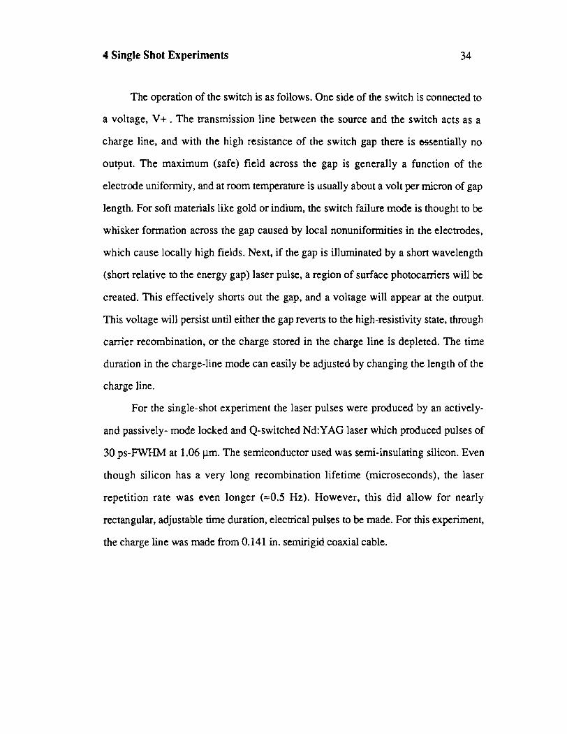
The operation of the switch is as follows. One side of the switch is connected to
a voltage, V+ . The transmission line between the source and the switch acts as a
charge line, and with the high resistance of the switch gap there is essentially no
output. The maximum (safe) field across the gap is generally a function of the
electrode uniformity, and at room temperature is usually about a volt per micron of gap
length. For soft materials like gold or indium, the switch failure mode is thought to be
whisker formation across the gap caused by local nonuniformities in the electrodes,
which cause locally high fields. Next, if the gap is illuminated by a short wavelength
(short relative to the energy gap) laser pulse, a region of surface photocarriers will be
created. This effectively shorts out the gap, and a voltage will appear at the output.
This voltage will persist until either the gap reverts to the high-resistivity state, through
carrier recombination, or the charge stored in the charge line is depleted. The time
duration in the charge-line mode can easily be adjusted by changing the length of the
charge line.
For the single-shot experiment the laser pulses were produced by an actively-
and passively- mode locked and Q-switched Nd:YAG laser which produced pulses of
30 ps-FWHM at 1.06 pm. The semiconductor used was semi-insulating silicon. Even
though silicon has a very long recombination lifetime (microseconds), the laser
repetition rate was even longer (=0.5 Hz). However, this did allow for nearly
rectangular, adjustable time duration, electrical pulses to be made. For this experiment,
the charge line was made from 0.141 in. semirigid coaxial cable.

4 Single Shot Experiments
4C(ii) Measurement Technique
Figure 4C.2 shows the apparatus used in this experiment. The hser [3] used
was an actively- and passively-mode locked and Q-switched Nd:YAG system, which
produced 30-ps FWHM pulses at 1.064 pm. Passive mode locking was achieved
through the use of a saturable absorber dye dissolved in di-chloro-ethane. The active
mode locking was accomplished with an RF-driven acousto-optic modulator. Single
pulses were picked out of the pulse train of = 20 pulses using a krytron driven tandem
electro-optic switchout. The repetition rate was something less than one Hertz, so this
was truly a single-shot experiment.
A coaxial charge line was used to control the length of the electrical pulse, and a
battery supply was used to control the amplitude. Different pulse widths could be
obtained by merely changing the length of charge line. The length of the pulse
corresponded to one round trip in the coaxial cable. This is due to the nature of the
photoconductive switch; even in the "on" state, the gap resistance is not zero. This
nonzero resistance gave rise to reflections which propagated back down the charge line
towards the charging resistor. Since the charging resistor was relatively large (10
k-ohm), the resistor behaved as an open circuit and the boundary condition at the
resistor was that of zero current. The second reflection was therefore a voltage pulse of
nearly equal magnitude, but opposite in sign, which effectively canceled the voltage on
the charge line. At the output of the switch, one observed the voltage pulse,
corresponding to one round trip in the cable, followed by several other reflections
which were very small in size, and were due to the non-ideal nature of the
terminations. The scope used to observe the high speed signals was a Tektronix
storage scope with sub-nanosecond resolution.

4 Single Shot Experiments 36
The high speed pulse was then conducted to the junction via 0.141 in. semirigid
coaxial cable and 18 GHz SMA connectors. Devices were placed in a glass helium
dewar with a liquid nitrogen outer dewar, so that the total propagation distance from
switch to device was about one meter. The end of the cable was pressed onto the
junction using a cross sectional slice of indium wire to make a cold weld.
Dye Flow Cell
0.141 in. coaxial cable
Figure 4C.2 Experimental setup.

4 Single Shot Experiments 37
Finally, another cable was attached to the output of the junction, and routed out of
the dewar to be terminated in a 50 R load at the storage scope. This allowed each laser shot - to be monitored, as the pulses arrived at the storage scope with very little degradation. A
laser shot with unusually low amplitude would result in a very small electrical pulse at the
scope and so could be ignored. Larger than normal pulses, however would not affect the
experiment as the Si switch was driven into saturation with this system.
The dc I-V curve for a particular junction was traced out using a home-built bias box
which operated at tens or hundreds of Hertz. DC biasing, as well as temporary device
grounding, could also be provided from the same circuit. Four-wire connections to the
junction were made using twisted pairs of wires inside the dewar, and twisted pairs of
coaxial cables outside.
In practice, assuming the liquid helium had been transferred in time to achieve a
functioning junction and that the laser was working, the experiment would be performed as
follows. First, a charge line length would be chosen and the bias voltage, Vdc, would be
set. Next, the bias current would be set to a particular value, and after the laser shot,
switching (or not switching) could be determined by checking the junction state using the
I-V scope. Finally the junction would need to be grounded (reset) using a push-button built
into the bias box for this purpose, provided the last laser shot had indeed resulted in the
junction switching into the voltage state.
After performing several runs using this procedure, it became apparent that the
junction could in fact be switched by the abundant RF noise present whenever the laser
fired. To cure this, all cables were wrapped in aluminum foil and then grounded. This
included the high-voltage lines for the laser flashlamps, as well as the cables associated
with the junction dc biasing network. Despite the fact that these cables were coaxial, it
appears that the sheath, which was stranded wire, behaved as a waveguide operated below

4 Single Shot Experiments 38
cutoff, but was simply too short to be effective. At the top of the cryostat, all bias wires
were fed through inductive femte beads. In addition, the dewars were enclosed in a double
mu-metal magnetic shield, and then grounded. Finally, the switch outpm was attenuated
using an 18-GHz 20 dB attenuator. This allowed the noise to be attenuated while the signal
amplitude was increased. The data presented in the next section were taken after these
precautions were taken.
4 Single Shot Experiments
4C(iii) Results
Experiments were performed using two different size junctions;large and small,
where the size was relative to the Josephson penetration depth, h. . The device parameters J
are given in Table 4C. 1. The mean free path for these lead films was 35 nm.
TABLE 4C.1 Large Area Junction Small Area Junction
Dimensions (1) 420 x 240 pm2 50 x 50 pm2
Area lo-7 m2 2.5 x 1 0 - 9 m 2
h. (approximately) J
3 0 0 p m ( $ < 1 ) 250pm ( h . > > l ) J
Critical Current Density 3.8 A/ cm2 5.2 A/ cm2
Critical Current 3.8 mA 0.12 mA
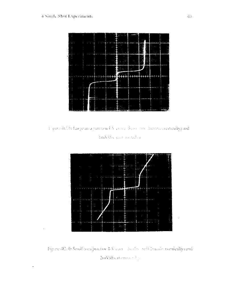
I-V curves for these same junctions are shown in Fig. 4C.3. The curves indicate
that these were indeed high quality junctions. Trapped flux could be freed in these
junctions by raising the entire experimental rig above the surface of the liquid helium
(and so raising T above Tc), so these curves truly represent the maximum critical
current.
Data were taken using a variety of pulse lengths as excitations, ranging from
less than one to several nanoseconds. A typical pulse showing very good signal to
noise is shown in Fig. 4C.4. The lower limit was defined physically by the smallest
charge-line which could be constructed. The nature of this experiment was such that
the result was a phase diagram. For values of the pulse width and amplitude which
were smaller than the critical value, no switching occurred, while those values which
were larger resulted in a switching event. The critical combinations of pulse widths

4 Singlc Shot 12upet.inlcnts
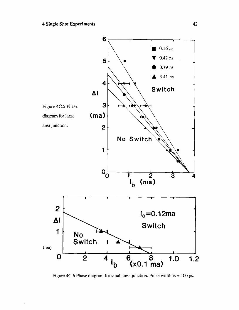
4 Single Shot Experiments 42
Figure 4C.5 Phase
diagram for large
area junction.
1, (ma)
m I
. . IO=0.12ma
1 * 2 4 6 8 1.0 1.2
lb (x0.1 ma) Figure 4C.6 Phase diagram for small area junction. Pulse-width is = 100 ps.

4 Single Shot Experiments
4D Flux Flow Theory
In order to model the results of these experiments, let us stan b p s i n g the the
equations proposed by Dhong and Van Duzer [17]. Using the pendulum analogy, the
minimum width control pulse, z , can be divided into two portions, z , the time
required to swing the pendulum to the critical point and, z 2 , the time required to
impart the necessary energy to the bob to overcome the damping. This situation is
shown schematically in Fig.4D. 1.
Figure 4D.1 Pendulum analog. €Ib is the applied bias torque.
The times zl and z2 are calculated to be (Ref. [17]):

4 Single Shot Experiments 44
For the large area junctions used in the experiment, C. = 16 pF, RN = 0.13 R, J
and IO = 9.0 ma. Using these values, one computes a value of r oFabout 4 ps.
Clearly, this is almost three orders of magnitude too small compared to the
experimentally determined values shown in Fig. 4C.5.
Given such a large disparity between the predicted and measured values, one
needs to seek another transient limiting mechanism. It has been known for some time
that large junctions exhibit flux flow behavior when the current bias is switched from
one value to another [24]. The origin of this flux is the self-induced edge field due to
the bias current. As the flux drags through the junction after a change in bias, the
viscosity it experiences results in a significant time delay. This viscosity is caused by
the finite junction resistance. To understand how flux is redistributed in a large area
tunnel junction, consider the diagram in Fig. 4D.2.
As shown in the figure, for a large area junction biased in the zero voltage state,
most of the current is conducted along the outside edges of the junction. After the
junction has switched into the voltage state however, the current becomes evenly
distributed, and so the magnetic field becomes linear. The location of the average field
is marked by the dots in each picture. After the switching event, the average location of
the field has moved a distance L.
To calculate the time required for the field to move this distance, we fust need to
know the Lorentz force:
f L = ~ v = J a B
The electric field is given by:

4 Single Shot Experiments
a
I (Before)
X
Figure 4D.2 Flux flow diagram. Note that it is the current distribution shown before
switching and magnetic field shown after switching to the voltage state. The average
value of magnetic field is shown as the shaded dot.
The energy dissipated is due to the normal current which extends one
penetration depth into the conductors, and so the flux flow resistivity is just the normal
state resistance:

4 Single Shot Experiments
and pf = PN
J P , L ~ ;. v=- L @B and so: z =- = - @B J ~ N L
To use equation (4D.7) to perform a sample calculation using the measured
values of the large area junction we need to calculate the current density:
I,, + A1 4 2 J =
A = 5 x 10 A/m
We can estimate L using the measured resistivity ratio (6.4): pl = 1.05 x 10-l5
!2m2 and p(300K)= 1.92 x lom5 Qcm, so the mean free path, 1 = p1 / p4K = 35 nrn.
Clearly, this calculation gives a much more reasonable result. In addition the
pulse width z is seen to be inversely proportional to the total current, so a plot of
inverse pulse width versus bias current should be linear. This is shown in Fig. 4D.3.
For all but small bias values, there is very good agreement with Eq. 4D.7.

4 Single Shot Experiments
A1 (ma)
Figure 4D.3 Large area junction results replotted.

4 Single Shot Experiments
4E Limitations Of The Theory
Given the somewhat surprising result that these junctions wereslower than
expected, some further experiments were immediately attempted. Namely, for a
material dependent phenomenon, it seemed reasonable to repeat the experiment with a
different material. This was attempted for junctions made with lead and varying
amounts of indium or bismuth. However, it soon became obvious, given the nature of
these lead films, that no useful devices could be produced.
In order to overcome this problem, two major decisions were made. First, it
was clear that a new source of devices was necessary. Devices, which were high
quality, fast, and even possibly recyclable were required to enable experiments to be
performed. Also, a laser system was required which would offer the speed, reliability
and ease of use that these new devices would require.
The first requirement was satisfied by the availability of lead alloy fabrication
facilities at the National Bureau of Standards (NBS) in Boulder, Colorado. I was
invited to make use of their facilities to produce virtually state-of-the-art Josephson
devices. This procedure is described in Chap. 6.
In order to be sure that the measurement system would be capable of
characterizing these faster devices, the Nd:YAG laser was replaced by the very much
faster (both in pulse width and repetition rate) laser described in the next chapter.

5 Electro-Optic Sampling
Electro-optic Sampling
This chapter opens with a brief introduction to the optics involved in these
experiments. Both the laser and the Pockels effect are described along with a new
detection scheme developed by the author for these experiments. This scheme was
required by the very small voltages produced by the junctions.
Next, the cryogenic implementation of the electro-optic sampler is described.
The development of this capability was essential to allow time resolved measurements
to be made on superconducting devices and circuits. This was accomplished by the
author in a series of steps, culminating in an unprecedented rise time measurement of
360 fs. Furthermore, it is shown that the frequency content of this signal exceeds the
energy gap frequency of the electrodes used in the transmission line.
Finally, a brief study of the propagation of these ultrafast rise time pulses is
presented. The purpose of these measurements was to insure that the pulses being
applied to the junctions were not distorted during the propagation from
photoconductive switch to device. The issue of signal propagation is an important
aspect of any high speed experiment and will be discussed further in Chap. 8.

5 Electro-Optic Sampling
5A(i) CPM Laser
The underlying speed of the electro-optic sampling technique is the direct result
of the laser used to make the measurement. This laser is the CollidingPulse Mode 1
Locked (CPM) system [3], and in its present form is capable of generating pulses as
short as 27-fs FWHM [25]. The CPM laser has been described in the literature, so
only a brief description of the version used in these experiments will be given.
A commercial Coherent ~ r + laser (Innova model 1-100-20) which produces
nearly 10 Watts of cw light at 514.5 nm is used as the pump for the CPM laser. The
argon laser is normally run in the range of a few watts and an optical feedback loop is
used to control precisely the output power and to limit the noise to about 0.3% RMS.
The CPM laser itself is a dye laser using both a gain medium, Rhodamine 6G
and a saturable absorber, DODCI (DiethylOxa-DicarboCyanine Iodide). These two
dyes are a well-matched set and are used together often in dye lasers. The CPM laser
however, is a somewhat different animal, as shown in Fig. 5A. 1. 1 5 14.5 nm Ar pump
DODCIodide Saturable Absorber Jet Rhodamine 6G Gain Jet
Figure 5A. 1 Colliding Pulse laser system.
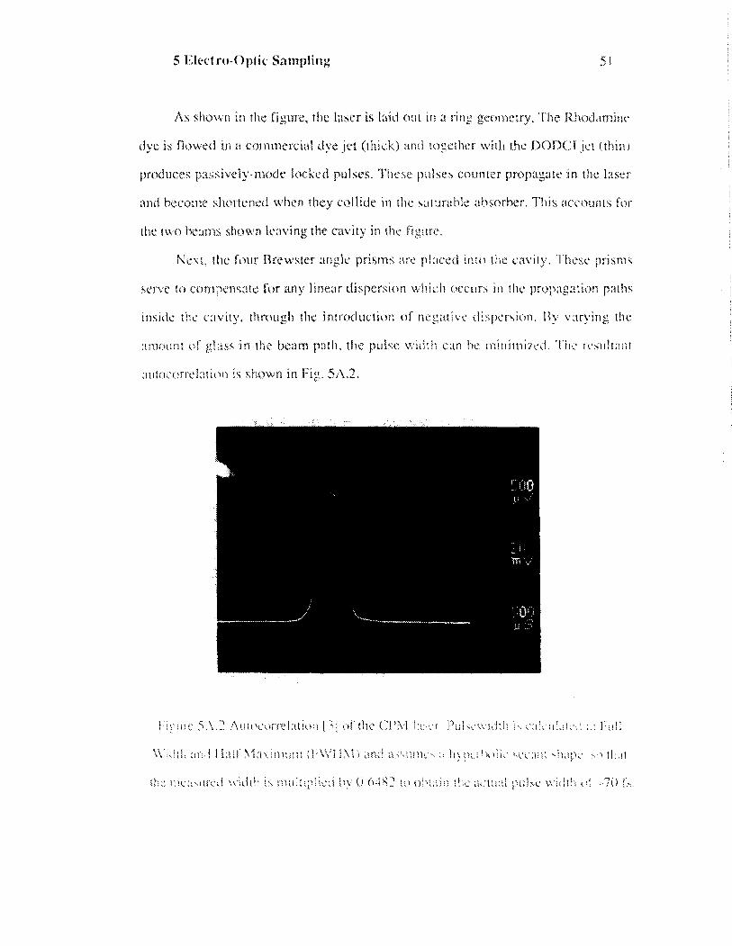
:IS ~lii>~v:i i t 1 the f'igr~1.2, t ! i ~ I ~ I S C ~ kiii! 0 ~ 1 1 i r I ririg $cc:)rfi::try. ' 1 . 1 1 ~ [<.hi:)~!ii~~:j~ir
tf>ve is flowed i.1) ii c ~ ~ i ~ l ' t ~ c r ~ i i i l dye jrt ( l l l i ik j and ~o;.cthi:i' witli thc 1:)01.)(:::1 j c t (t!lirli
proc!uces \!:tsivtl;).'.n-tc.ide 10cl :~d 171~1~~ 's . Ttli'sc pi11st.h i:oltnrcr 1zropag;lte i n ttic 1:ist.r
;inti bi.cori:e slii~rtcsnri'; when t1.1ey cc~lliclr ir~ tfie \a tur;~b!r: absorhi.:.. I'!iis ~Icci~!lll~s f \>r
ltic ti\'(, JV:1~:is stl!.!wu I.c:\t?ing rhe cavity in il-ic lig.:trc'.
Nest, tlic fitur I<~-ewster. :trigli pristns ;\re p'!;~cc.ci irlro t l i i : crnvily. 'I'I.rcst. prisms
srh!.v~ ti') cOnll>i'n<;iI< f ^ ( ~ itfly li17e;11- dispersion wP!i;.17 i.tccL:l.:, i!i !he ptc?~?:~~:i:ic!n p ~ t ! l j
ir1sii.1~ t!:c c:~vi:y. t l~ rc~ i~g!~ t 1 1 ~ iritrctc1~1ctio;i of' r~eg;~.r;\,c c l ispc~-~ior~. l3y v:~ryi~)g tlic
:I;?IOL::.I t {.>I. !!!;is i n lhe t x a m p ;~t l~ . t l ~ c ~ L I I S C ; v:,~t.::!: c;~tl !)c ~i~ : i~ i i~ i~ i~~ :c l , '171c I . ~ S I . I ~ ~ ; I ; . I I
:~ i~ t~ .~~ . :o r~ t : j : i : i i .~~ i is S!IO*+V~I 111 Fi;;. 5:\,2.

5 Electro-Optic Sampling 52
Although the record for this type of system is 27-fs FWHM, the stability is
much better for the longer pulse widths. The exposure time for Fig. 5A.2 was 1/2
second and there is virtually no deviation from a single trace. The reason more
laboratories do not make use of this very fast source is the dye system itself. Both
dyes have unknown health hazards, and in particular, the DODCI is very short lived.
If no particular precautions are taken, the DODCI has a useful life of about two weeks.
In order to extend the useful life of the dye, several factors were identified as
contributing to the dye dying prematurely. Basically, air (oxygen), water, heat, old
dye and light all have detrimental effects on the dye lifetime. To mitigate these effects
slightly, the following changes were made. A cooling network was placed into the dye
reservoir, although the temperature setting had to be warm enough to prevent
condensation (just below room temperature). All fittings and hoses were replaced with
either 3 16 stainless steel, or non-staining tubing. A non-staining tube is one that can be
completely cleaned after immersion in the dye: teflon is, tygon is not. The filter
assembly, which was used to remove air bubbles from the dye, was replaced by a
disposable cartridge type with a cleanable housing. Finally, some tubing was replaced
with a type that had a black outer tube. The result of these changes was an increase in
the average dye lifetime by a factor of two.
While the Rhodamine dye was considered relatively inert, it turned out that it too
suffered the same problems as the DODCI, although not to the same degree. In fact it
turned out that the brass fittings used were tinting the dye green. Many of the same
improvements have been applied to the Rhodamine system and the dye can now be
expected to last many months.

5 Electro-Optic Sampling
SA(ii) Pockels Effect
Once an electrical signal has been generated using a CPM laser pulse and the
photoconductive switch, it has to be detected using the second optical pulse from the - CPM laser. The transformation between the electrical regime and the optical regime is
accomplished through the use of the Pockels effect.
Basically, the Pockels effect alters the state of polarization of an electro-optic
medium in the presence of an electric field. If the medium is placed between crossed
polarizers, the birefringence results in a change in intensity. Since this change is due to
changes in the crystal on an atomic scale, the speed can be as fast as a few
femtoseconds.
Specifically, if polarized light is incident on an electro-optic material, the two
orthogonal polarizations will each see a different index of refraction. For small
distances, 1, the total phase shift. is:
where h i s the free space wavelength and An is the birefringence. The output beam
will have a net polarization change of 6. This change of polarization can be converted
to a change in intensity by placing the electro-optic modulator between crossed
polarizers. The change in intensity can be maximized if the input beam is oriented with
a 45 degree polarization. In that case the transmitted intensity, I, will be:
where IO is the intensity of the input beam. The transmission is just Q, and is plotted
in Fig. 5A. 1. The transfer function is most linear in the central region around the 50%
transmission point. However, the modulator will have a certain amount

5 Electro-Optic Sampling
0 v Voltage 7t -
2
Figure 5A.1 Modulator transmission function
of static birefringence, even in the absence of an applied field. By placing a variable
retardance device in the beam path, between the polarizers, it is possible to "optically
bias" the modulator to this 50% point. In these experiments this was accomplished
with a commercially available Soleil-Babinet compensator.
In practice, a given modulator can be calibrated by using the compensator to find
both the minimum and maximum transmission points. The 50% point is then defined
as the midpoint. Next the voltage scale can be calibrated by simply applying a known
voltage and measuring the resultant change in intensity. Since the half wave voltage,
V,, is usually in the kilovolt range for the modulators used in these experiments, the
assumed linearity is a very good approximation. Finally, the specific choice of
material, lithium tantalate, is based on previous experience, and is the best
compromise, among the competing qualities of sensitivity, robustness, ease of
processing, etc.

5 Electro-Optic Sampling
5B Microvolt Sampling
As shown in the previous section, one can change the transrniwd intensity
through a modulator by an applied voltage. The specific implementation used in these
experiments is shown in Fig. 5B.1.
Differential Input Amplifier
Figure 5B.1 Sampling system schematic. Excitation beam is omitted for clarity.
In absolute terms, the change is very small. Most electrical signals of interest are
in the volt or even millivolt range, whereas the halfwave voltage for most of the
modulators used was in the kilovolt range.


5 Electro-Optic Sampling 57
As shown in the figure, there are several features, which may be due to various
resonances inside the cavity (they are not present in the argon laser spectrum), but the
general behavior is l/f until the noise floor is reached at about 2 o r 3 MHz. The
spectrum was taken using an EG&G FND-100 photodiode which was used as a
detector for a Tektronix 7 104 spectrum analyzer (0 - 5 MHz).
From the preceding discussion, it would appear that the obvious solution would
be to operate the lock-in above this frequency. However, the limit for the PAR-124A
being used was only 100 kHz, so the improvement was not dramatic.
The next step was to change the lock-in. This is not quite so simple, as the only
commercially available lock-in which runs at high frequency (PAR-5202), had very
poor performance in our application. In addition to inadequate overall sensitivity, this
unit lacks the capability to perform a differential measurement. As shown in Fig.
5B.1, when the two polarizations are separated in the final polarizer, an analog
differential amplifier is used to cancel the noise partially, and to increase the signal
level (note that even in the absence of noise the signal level would be increased by a
factor of two).
However, as the frequency increases, this differential amplifier becomes a very
complex beast indeed. In conjunction with the 5202, an Analog Modules GaAs
differential amplifier was used, and much of the data reported in the following sections
used this scheme. For those experiments the modulation was limited to the 2-4 MHz
range, as some other link in the detection chain experienced a frequency roll-off,
probably the detector diodes themselves.
The next incremental improvement was made by replacing the 13-MHz Analog
Modules amplifier with a Tektronix oscilloscope. The particular scope, a 7000 series,
allowed two signals to be subtracted, as well as an upper bandwidth limit of 20 MHz.
This bandwidth limit helped to limit the noise presented to the lock-in outside the

5 Electro-Optic Sampling
passband.
Finally, an improved solution was found. On the one hand, the laser has a noise
floor at 5 MHz, and on the other hand, the best commercially availablelock-in only
runs to 100 kHz. Therefore, a mixer was constructed to mix down the high frequency
modulation to match the 124A lock-in. This method yielded improved signal to noise,
despite the =5 dB conversion loss of the mixers, due to the far superior sensitivity
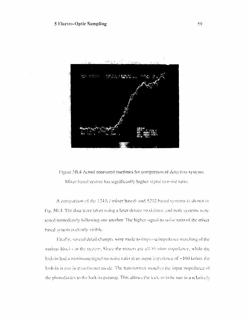
(two orders of magnitude) of the 124A. The layout is shown in Fig. 5B.3.
Signal source High Frequency Differential Input Amplifier L.O. Reference
b To Display
Detectors
(a) High frequency differential amplifier used with single mixer
Mixer
Mixer
(b) Individual mixer scheme using low frequency differential amplifier in lack-in.
Signal source
Figure 5B.3 Mixer schematics
Lock-In Reference + b
To Display

5 Electro-Optic Sampling 60
low noise regime, and still operate at a frequency above the usual noise sources such
as 60 Hz line noise.
In addition, matching of the diodes to the mixer inputs was addressed. The
diodes are rated at 350 MHz bandwidth into 50 ohms. Clearly, this bandwidth is
unnecessary, so the diodes were terminated into =1 kohm to increase the signal level
at the expense of the bandwidth. This practice may in fact be the reason for the upper
limit in bandwidth to the few megahertz frequency range.
The signal source used originally was an HP test oscillator which was in turn
used as a reference for a digital circuit which produced the lock-in reference, local
oscillator (L.O.) and modulation signals for the photoconductive switch. This system
had an upper limit of 2 MHz defined by the requirements placed on the digital
electronics. To overcome this limitation, an HP 3326A has been used. This system can
produce both the reference and L.O. signals, as well as the modulation signal. Even
with the bandwidth limitations elsewhere in the system, this mixing scheme has still
been run as high as 3.5 MHz.
5 Electro-Optic Sampling
5C Cryogenic Implementation
In order to characterize superconducting electronics on a picosecmd timescale,
the electro-optic sampling system had to be modified. For the initial experiments, the
modifications were minimal: a helium dewar was used for the experiment, and long
cables were used to route the signals into and out of the cryogenic environment.
However, it was always the intention to construct an integrated system, although this
was achieved in a series of steps.
First, a dewar had to be designed for such an integrated system. This was
accomplished by a special design with a total of four in-line windows (all neither
crystalline nor birefringent) to allow laser beams to pass through undistorted. The
inner windows were fused silica and the outer ones were generic optical quality glass
with no coatings. In addition, the liquid helium which is placed in the dewar must also
be non-distorting, so the temperature in the dewar must be reduced to the superfluid or
h point (by reducing the pressure in the dewar). At this temperature (2.18K), all
boiling stops in the liquid, except for a thin layer at the surface. This technique had the
added advantage of excellent thermal equilibration, as no temperature gradients are
allowed, which may help to prevent thennal birefringence in the sampling crystal.
The fust experimental step was to place one part of the sampling system into the
cryogenic environment at a time. The sampling geometry used was a coaxial type with
a microstrip geometry sampling crystal placed in a cut cable. This layout is shown in
Fig. 5C.1. Using 0.085 inch semirigid coaxial cable and 40 GHz connectors, a rise
time of 16.4 ps was measured, as shown in Fig. 32.2, in a cold (liquid helium level
just below the sampling crystal) dewar by placing the sampling crystal into the dewar
WI.

5 Elect ro-Optic Sampling
Figure 5C. 1 Coaxial sampler geometry. Sampler was built from 0.085 inch cable
Figure 5C.2 Cryogenic sampler rise time of 16.4 ps measured with cold crystal
and room temperature signal source.

5 Electro-Optic Sampling
The rather long rise time was a direct result of the long cables (several feet) required to
route the signal from the room temperature switch into the dewar. -
The next step was to integrate the switch and the sampling crystal into the same
structure. Several structures were considered, and the first choice was to use the
reflection mode geometry. In this geometry the sampling crystal is coated with a
nonconductive dielectric reflective coating. This geometry promised several
advantages. First, it had already been demonstrated at room temperature. The very
short propagation distances had led to a rise time of 0.75 ps at room temperature [27].
To improve on this basic structure, the geometry of Fig. 5C.3 was used.
Excitation Puire
Figure 5C.3 Gapless sampling structure. The high reflection coating was a dielecmc
stack, which provided both high reflectivity and electrical insulation. Both the probe
and excitation beams could be moved up and down the transmission line.

5 Electro-Optic Sampling 64
This gapless structure allowed the switch to be defined by the laser excitation
beam, and not a predefined gap. In addition to allowing even shorter propagation
distances, this structure allowed more flexibility in changing the propagation path
length. A sampler made in this geometry using lead electrodes had a measured rise
time of 1.8 ps at room temperature. However, it became apparent that several
problems were associated with this design, even at room temperature. Specifically, the
signal-to-noise ratio for this geometry was generally much worse than other, more
conventional layouts. This may have been due to the double pass geometry, stress
birefringence induced by the spring clips used to attach the sampling crystal, or
retro-reflections back into the laser cavity. In any event, after many attempts, the
decision was made to change to a more conventional geometry. However, this design
has been adapted recently by Duling, et a1 at IBM who are taking advantage of the
gapless structure [28].

-['he ;~i[~rr~:iii: geometry which was t.hosetl has also b e e . ~ used it( room
tirrl:i?r'sactlre, h;lvinc ., ;I nreastlreci rise tirvle of .IAO 1's (51. 1 1 1 dcsigrlir~g :i vel-sion f o r Ic:,w
I ( ; . I : I ~ ~ ~ I ~ ~ L ~ \ I I ~ c i!l?cr;~tii>r~, srt\;ttr;~l cfesi~ri criicri;t I;:~i.t to !.x r r ~ e t .
I'ir.;:, t l ~ s~n;tllsst gc.c.~rnctr\- curt~c1111y :tv;~il:ifnle wns ilscd. In t l~is design, the
swirch ar;cl s : ~ i ~ ~ j - ~ l i n g cryst;\! were. cdgc.pnli.xhcc! tinti1 ii 1:1:tlirlg st~ri'nce wits prod.\rcc.ll
\ : i t t l :nict.ort c~nilbnlri~y. 'I'hese \vc..r.c i:ticn glued L?OWI\ (.>II:o ti ~~licrosi 'ope S I hie, :tnd
~;~l-f:ize ~ ~ ~ ! l i ~ i . c t l , 'Ilhe rcsl.ilt;int str11i:tur'c w:~s sct iinift?rru tt131 r~lc:;tl elcctrr)cf es coulci ht.
i'\i:!jjr!r;~tr*<l ~~~r t t i r i t~o~is lp ;ICI+OSS the iri i t-~~*f ' t~c.c~. -TI-lis ;.-. ,a sIi;.tii1:~ i l l Fi?. 51::). 1.
Iqigu:.~ 5D. 1 F1l~oto~~-~i~hrngr~i~~l~ of i~ttegrritcil strucrure. I mcs arc 20 p.ni spncc.ll
by 2(1 ~ i m - Ttte gap in ihc upper cor-~cltlctc>r fon i~s the pho t ix t~nd~~~ t iv t : switch.

*I'J.ic s;:!ll;)i:li! ' : t i . t i i ' ~ , : ~ ! . ~ ~ ~ ~ 1 . c f : ! t > t . i ~ ; j 1 ~ ~ ! !f~ir:g !.;fInio!i\h~,rr;ti?hir.3]jy defilleil
' , 1ir;c.; ;!:lil I : i i l i r . i r~ l ~n~.k:iiliz,itio~;. I ' l i i~ srru:;:!iri. wns thz:~ char:tcterized usirlg ~ l \ c C7'.\,1
I L L S C ~ s;!~sI~)!cs : i ~ ~ d S ~ I ~ I ~ ~ S C ! I L ~ , . ~ Ii<:li\1111. 'I"\Ic : I~C: \<LI~C<I 1 . i ~ t i ~ v v 01. '360 f.s is ~t>i1\),:11 111
Fig. 511.3. 'l+t:e ji I tery I I : ! [ L I ~ ~ CI~' I tic ~I.:~cc' is (111~: to :I:e vc1.p ic.ru: ~ilr:i. c.ons!;llit ui:(?(.t (.)II
. , l l~e 1oc.k-ii.:, ts.t;;cI: \V:\< ~ie i . cb~ i ' \ ; i l t k t i)y ~!IC tiish ~xini inunl spced of 1216 c.~ptii;!i c!c.l:~>*
liiic.. In c!rllzr v:or.;ls, !;~!IL~C [tic. t n n s t ; t r i o r ~ ~ritgc rl:o~lc.c.i so rapitily, rht: lock-iri !,;:!i 10
l1 :,.t,c :, ,,.&,-,,: ,. , r<~l : : i \ \ ~ i r l ~ ; ~ ~ c~,,v>?;\:!r;[ I!) t:!ri:!?S ;:.I ~'csc)]\%c ihc. rise 1il:lc.

5 Electro-Optic Sampling
0 1 2 3 4
Distance (mm)
Figure 5D.3 Measured dispersion on superconducting transmission line.
electrodes. These results gave some startling information about the performance of
superconducting transmission lines.
Consider the energy gap of indium. This can be related to a frequency by E=hv,
which for indium is ~ 2 5 0 GHz. Clearly, a rise time of 360 fs has frequency

5 Electro-Optic Sampling
components close to 1 THz. What this means is that frequency components well above
the gap frequency are apparently still being conducted. By comparing the
superconducting structure to the same geometry with higher conductivity gold
electrodes, it is likely that strictly normal electrons are not the sole conduction
mechanism. A numerical calculation was made to simulate an experimental dispersion
curve using only modal dispersion to model the system, and excellent agreement was
achieved. A more detailed discussion of these simulations is presented in Chap. 8.
The importance of these results should not be understated. Namely, that
superconducting transmission lines can conduct frequencies well above the energy gap
frequency means that terahertz frequencies can now be conducted from one device to
another with little or no distortion. By using materials and geometries optimized for
minimal dispersion, circuits operating in the terahertz regime are clearly feasible. In
fact, for a "real" machine with finite propagation distances, the importance of a
theoretical "zero rise time" device is overshadowed by the need to propagate that signal
from place to place.

6 Cryogenic Results
6 Cryogenic Results
- This chapter opens with a review of the design requirements for the coplanar
strip transmission lines used in these experiments.
Next, the cryogenic probe is discussed. While based on an NBS design, the
author's version differs significantly in its usage of only one very high speed
transmission line to service all the circuits on a given chip. The advantage of this
design is a tremendous decrease in the thermal loading of the helium bath by reducing
the number of heat pathways to room temperature.
Two sets of experiments are described in this chapter, and they are divided into
sections: quasi static experiments (Secs. 6D and E) and integrated experiments (Secs.
6F and G).
In the quasi-static experiments, the sampler and photoconductive switch were
both in the room temperature environment. This placed a lower limit on the pulse
width that could be delivered to the junction due to the long signal paths into and out of
the dewar. These experiments provided a base line against which the integrated
experiments could be compared.
For the integrated experiments, the switch, junction and biasing line were all
integrated on a single substrate. In addition, the signal path between the switch and the
junction was minimized to insure an unprecedented rise-time pulse would be delivered
to the junction. The signal path length was in fact smaller than the path length which
resulted in the 360 fs rise time reported in the previous chapter. This experiment
represented the highest level of integration ever attempted using electro-optic sampling
-- at any temperature, and the first time a subpicosecond rise-time pulse had been used
as an excitation for a device of any kind at any temperature.

6 Cryogenic Results
6A Transmission Line Theory
For these experiments coplanar transmission lines were used-to facilitate
fabrication. In order to maintain a constant 50-ohm impedance through the entire
structure, the lines as well as the contact pads were designed for this impedance. A
quasi-static analysis was carried out by Wen [29], although this analysis neglects finite
substrate thickness.
The characteristic impedance, 20, for a transmission line is given by:
In the expression for the phase velocity, vph, an average value of the dielectric
%(substrate) constant is used, assuming an air superstrate, so that eeff=
2 + , I .
For coplanar waveguide the capacitance per unit length is:
where aland bl are the waveguide dimensions as shown in Fig. 6A.1 (zl-plane).
bl el
Metal
Figure 6A. 1 Coplanar waveguide geometry (zl -plane).

6 Cryogenic Results
Next, in order to find the characteristic impedance for a coplanar strip -
transmission line, a conformal transformation is made into a rectangle, such that the
dielectric fills the interior. This mapping is shown in Fig. 6A.2 (z-plane).
-a-jb a-j b
Figure 6A.2 Conformal map into z-plane.
In this mapping, the dielectric interfaces are now on the top and bottom
surfaces, and the electrodes are on the sides:
where A is a constant. The ratio of a/b can be found by using the integral:
"1
and the following formulae can then be found:
a h = K(k)/Kf(k)
where K(k) is the complete elliptic integral of the first kind and:
k = al/bl and K'(k) = K(kt)

6 Cryogenic Results
Substituting these expressions into equations 6A.1-3, the characteristic -
impedance becomes:
For a given impedance then, the tabulated values of K can be linearly
interpolated to yield a value for the line dimensions. As an example, for 20 = 49.82 $2;
k =0.037 and 8 = 2.12', K = 1.57137, K' = 4.69405 so that al/bl = .33476 and
and so a/b = 0.038.
For a minimum dimension of 5pm = 2a, then b = 63.29pm. In addition, to fit 5
contact pads on a 114 in. chip, pads were chosen to be 47.03 mils wide with
corresponding gaps of 3.72 mils. This maintained the 50-ohm impedance through the
entire structure.
While this strategy represents an optimization, it should be noted that it is, as
stated in the opening paragraph, a quasi-static approach. The reality of a high-speed,
broad-bandwidth structure, is that different frequencies will experience different
impedances. Furthermore, the abrupt change in dimensions in the transition between
the transmission lines and contact pads also represents a violation of the "gradual
change" rule of microwave design, namely that changes in structure should be gradual,
relative to a wavelength. Despite these shortcomings, this design, along with the probe
design discussed in this chapter, proved to be very workable.

6 Cryogenic Results
6B Sample Design
- Devices were constructed at NBS in Boulder, Colorado on two different
occasions, and the brief outline given here summarizes the procedure used.
The first devices constructed were subject to several design constraints. As
described earlier, the high speed signals were to be routed into and out of the
cryogenic environment. This required the entire structure to have as close to 50 ohm
impedance as possible to minimize reflections. To accomplish this, everything,
including the contact pads, was designed to have 50 ohm impedance. In addition, in
order to test any devices at NBS, a particular contact pad pattern had to be used in
order to mate to existing NBS probes [30]. Specifically, test devices were fabricated
around the perimeter which mated properly to the NBS test probes.
The basic fabrication technology is the IBM lead alloy type [31.]. In addition,
niobium ground planes were available, and this layer was patterned into a backing
layer for the contact pads. The basic layout is shown in Fig. 6A.l. Window Layer (300 nrn SiO)
Top View
Base Electrode (250nm Pb/ldAu)
Side View Silicon Substrate -
Figure 6A. 1 Tunnel Junction Fabrication

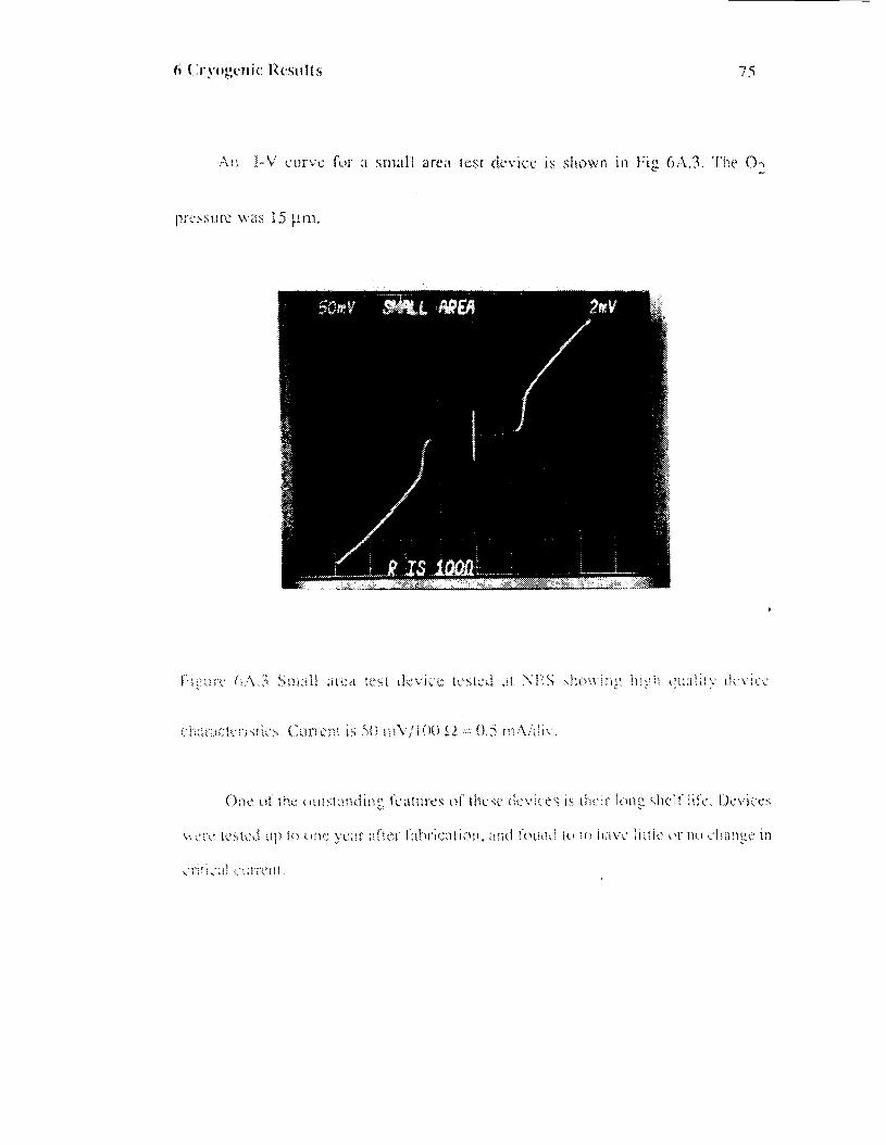

- 7 I he prt.)bt. for tliis t\perimcrlr was 1~;lscci (311 a desigtl tjy C.A. I-t;u~~il.ton (Iicf.
30) of KAS. 'I:'l~is \i.;ts tlotlc for: sever:rl reasons, First, suc:h a design i ~ l l o \ \ ~ c d testing
of tleviccs to Dc sccon~plishrd a t NBS during the t;it~ricntinn psoces. It ;ilso :~llt.~\\lcif
e:tsy cllangil~g ol'ctiips ns rhis \\;as ;t "drop ill" design. Firi:\lly, t l l c tlesig~l ~ t ~ u l i i easily
l,e nlodifjcd lo slli!fch [he cij(;'sign [!Ic'oI-~ ~?t*t's~rltt'(I it1 rllis i'h;lplcr.
S1snti;rt-d circuit board nir~terinl (Cj-. !I)) \?:as used its a st.~bsrr.;t:c f(l:- tllc cliip
c;trricr. U~r):l!iii l i l c..i?ppe~. il:;ts used k)r the ~~\c t a l l i i . a t i~~ t~ , as r l l i i tns~eri:il ~ x ~ t i . i ~ ~ t ; ~ i s ~ : : i f \ :
. . s;~!.:~ig,~t?c$s CI;CII a; . rr*,!~,x!~?.:ii(: .. I C I ? ~ ~ ~ L ? ~ ~ I ~ I ; Y ~ ~ S . -Y]I~: I i r l~ : , \3!et-t !Lik:ri~:;)l,cd :.1si112 ( \ I ? S;III:C
pr.cwcduscs as 51;. t i l e cl:ips t l~cn~se lves~ est:tlp~ tt:;~t rhc I-cticlcs wcse ~rscil as t!lc t l l ;~sks
(rstt~er ttlart bcing, ~.':d~.icc~i, QII :1 stel) nnii rrpcar c:t;nti.~.t\ Tor cfhil! 11:;t:). ' 1 9 1 ~ l;t\.t.ra~ i r i rhc
c;irrii_.r is shown in Fig. OC. 1.
Figure hC. 1 Chip carrier substsrt~e. (:hip i h 0.25 in. stlunrr.

:I< 2\10;? 11 ir l rl~z i:pti:-t, only orit* kct (IS tr:in\tui~sion lincs i;~bric:~reri on the
t,:lt)tll;~\c. sin;^' t l~c 1/( lint-, v.erc 0.11 1 iil. s(:~t~irisid c:tblc, tn\~ltil~le littcs woi~l,l 11:tvc
bccn ; i l l cxct.\\;\ c thcr:l::rl ;o:it1. ~ 1 1 x 0 shown i l l the fipurt i \ a flcsible co:txi;;l c:tt)lc
de:,tg~lt.cl :I) 1ut)vlt.l~ ii (1~. t>::t.: to the c~pc.rir~lt.r~r
l'hc ~~onta1.t p:rd t.a~.h line was li31nlt.d hy l~fting rtle cclgc o f tllc coj~pcr st1;p.
nrld instrring it stn:i11 rlian1t.rt.r wirc twr~cuth it. 'l'tle stnp w;is then rttllccl ()\el the ;\Ire
t i t i ! t i c I o r I I I In .~dditlolt. ttlc ~i~iituin \>lot> I ~ . C ' ! I I I I ~ ~ ~ I ~ *
\ \ ' I \ k:W\! t o ~ i i l l ' l l ! L t ! the c ~ ~ 1 l t : ~ c t ~ 0 1 1 tilt? ci11;> \IlO\~tl or1 111c ~\,111!;~lv 111 1Iw
l ~ t ~ ~ ~ l ~ ~ ; 2 r : ~ ; ? l l
I:\tr ti)<: c l l :~) L ' 3 J l ' l t r itw11 .̂ a not;t*l techntil~:e Wib\ t~\t!tl \vhi~.h . I [ ~ O \ L Z ( ~ , I ( : the
\ l ~ ~ l \ ~ ~ i l ' ~ ~ l i ~ : ~ ~ I I I L ' \ Oil : ! l ~ ~ I l l j J 1 0 f~ C : L ~ ~ I Y ~CL 'CSW~ \ ~ i ( h 0 1 1 1 ~ OIX st'! Of l!(j II?\C~.. '1
. ir t .~I~g~l;ict~t i j ~ I O \ V I I 1t1 1'1:. iK'2

6 Cryogenic Results
As shown in the figure, the two large thumbscrews were used to hold down a
movable fiberglass (G-10) chip holder. In this way, the chip holder could be moved
relative to the substrate, to allow each of the transmission line structures on the chip to
be aligned with the output lines.
After the chip had been positioned, a brass block and Be-Cu spring were placed
on the back of the chip to hold it in place. The brass block also contained a small
resistor, which was used as a heater to drive trapped flux out of the junction. Behind
the brass block was a plate and two threaded cylinders which held the block in place.
These are shown in the right side of the photo. The small square is the 0.25 in.2 chip.
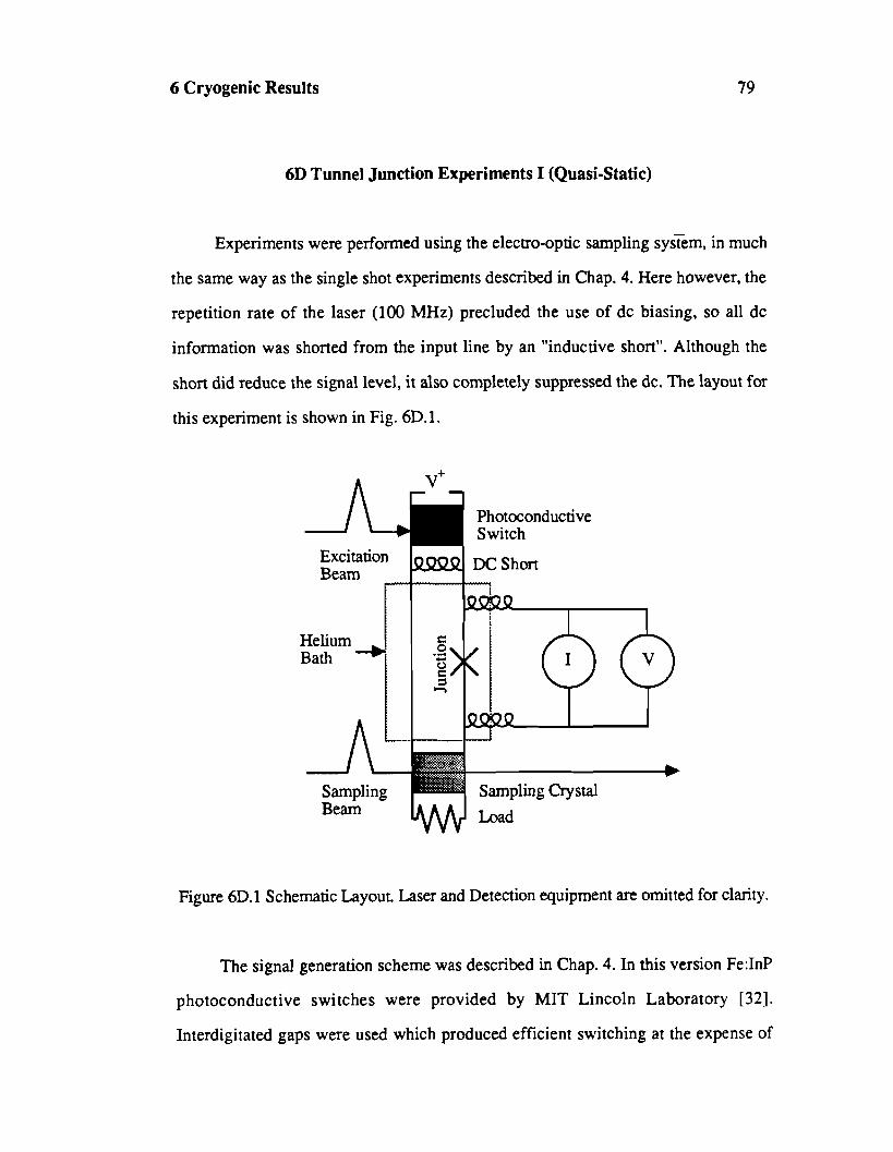
6 Cryogenic Results
6D Tunnel Junction Experiments I (Quasi-Static)
Experiments were performed using the electro-optic sampling system, in much
the same way as the single shot experiments described in Chap. 4. Here however, the
repetition rate of the laser (100 MHz) precluded the use of dc biasing, so all dc
information was shorted from the input line by an "inductive short". Although the
short did reduce the signal level, it also completely suppressed the dc. The layout for
this experiment is shown in Fig. 6D.1.
Excitation Dc Short Beam
Helium
Figure 6D.1 Schematic Layout. Laser and Detection equipment are omitted for clarity.
The signal generation scheme was described in Chap. 4. In this version Fe:lnP
photoconductive switches were provided by MIT Lincoln Laboratory [32].
Interdigitated gaps were used which produced efficient switching at the expense of

6 Cryogenic Results 80
some speed. These devices were mounted in an alumina microstrip carrier, and so the
charge lines were also constructed in this geometry. Charge lines of various lengths -
could be connected and disconnected in a matter of minutes using conductive silver
paint. An actual measured output signal from one of these charge lines is shown in
Fig. 6D.2.
Figure 6D.2 Measured Fe:InP switch output with charge line attached. The slower
portion of the rise time was due to reflections within the sampling crystal.
As shown in the figure, the rise time (80 ps) was limited by the propagation
distance. The detector used for these measurements was a coaxial design and nearly
identical to the one described in Chap. 5.
Switching thresholds were measured directly for these devices by noting the
- change in impedance that accompanied a change of state. As shown in Fig. 6D.3, this

6 Cryogenic Results 8 1
change in impedance or reflection coefficient, results in turn in a change in the
measured output voltage. This change in impedance is due to the change of the -
junction from the zero-resistance to the finite-resistance state. The results for various
pulse widths are shown in Fig. 6D.4.
applied switch voltage Vc (V)
Figure 6D.3 Output voltage as measured with the sampler, versus applied voltage. As
discussed above, the change in slope corresponds to the junction switching threshold.
The straight line behavior in Fig. 6D.4 is a clear indication that the junctions in
this experiment are still behaving in an essentially dc manner. This can be confirmed
by calculating the minimum pulse width for these devices using the model of Dhong
and Van Duzer (Ref. 17). In this model, the minimum pulse width consists of two
parts: a phase rotation time, TO. required to drive the phase across the junction by
approximately 7112, and a rise time, T ~ , required to initiate a nonzero asymptotic dc

6 Cryogenic Results
MAXIMUM BIAS CURRENT (mA)
Figure 6D.4 Threshold pulse height plotted versus bias current. The intercepts at both
the vertical and horizontal axes correspond to the dc critical current.
voltage. The term Z~ is determined by the capacitance and critical current of the
junction. In the pendulum analog, this is the time required for an impulse to push the
bob to just over the first half rotation. In the worst case analysis, where the bias
current, Ib, is zero and the pulse current, I is just equal to the critical current, 10, and P'
light junction damping, the minimum pulse width is (see section 4D):

6 Cryogenic Results
where CJ and cDo are the junction capacitance and flux quantum respectively.
The rise time, on the other hand, is determined by the time required for the
junction to overcome the damping and so it is da ted to the normal state resistance,
Rn. This additional time is:
The total pulse width required is T = 20 + f1 and for the case where Ib + I = P
10, T can be estimated using the experimental data of CJ = 50 pF, Rn = 0.13 f2, and
IO = 9 rnA to be approximately 6 ps. Since the shortest pulse available experimentally
was = 170 ps, the RSJ model would indicate that the junctions behaved with a
threshold essentially that of the dc behavior, as indicated in Fig. 6D.4.

6 Cryogenic Results
6E Indirect Measurements (I-V)
Using the I-V measurement apparatus, it was possible to measure the I-V curve
for a junction with and without the presence of the high-speed excitation. Essentially,
the junction would mix down the high-speed excitation to the frequency of the curve
tracer (normally tens of hertz). The advantage of this technique is that critical current
values could be directly determined in the presence of the excitation. Figure 6E.1
shows several I-V curves taken under varying levels of excitation.
Figure 6E.1 Series of oscillographs showing two wire I-V curves for a number of
increasing pulse heights (a to d), all having the same duration. The vertical scale is 5
W d i v and the horizontal scale is 5 mV/div.

6 Cryogenic Results
The entire I-V characteristic was slanted due to resistance of the wires used in
the two-probe I-V measurements. Two-wire measurements were made tominimize the
impact of the tracing apparatus on the high-speed signal paths. In the absence of
excitation (Fig. 6E.3a), the I-V curve was that of a high-quality hysteretic tunnel
junction with leakage less than 50 PA. The second switching in these curves was due
to the larger (shorting) junction described in Sec. B of this chapter. When current
pulses were applied, the entire I-V structure became asymmetrical (Fig. 6E.lb and c).
In the direction parallel to the pulsing current the junction switched at a bias less than
IO. This situation was experimentally found to correspond directly to the impedance
change shown in Fig. 6D.3, providing a separate measurement of the switching
threshold Finally, at large pulse amplitudes, the junction stayed in the resistive state,
as shown in Fig. 6E.ld.

6 Cryogenic Results
6F Tunnel Junction Experiments I1
- In order to time resolve the switching event, the integrated geometry of Sec. 5C
was adapted to the experiment with new devices fabricated at NBS, Boulder. In this
iteration, however, the substrate material was GaAs (undoped), which allowed
photoconductive switches to be fabricated in situ. The switch (50 pm gap) was
fabricated very close to the junction (about 70 pm). The measured 360-fs rise time
discussed in Chap. 5 corresponds to roughly the same propagation distance. The pulse
width was controlled by the length of charge line on the chip and for this design was
about 10 ps. In addition, an inductive (meander) line (10 pm) for I-V curve
characterization was fabricated directly on chip. A photomicrograph of an actual
sample is shown in Fig. 6F. 1.
The junction output was connected to a 50-Ohm gold coplanar stripline
fabricated on the sampling crystal through 18 pm gold wire bonds. In order to
minimize the propagation distance, the original output contact pads were cut off, using
a dicing saw, and bonds were made directly from the superconducting electrodes to the
gold lines. Bonding to the superconducting electrodes proved to be very difficult. The
Pb alloy is a soft material and was fabricated in a thin layer on the chip. Much worse
however, were the PbBi lines, as these were covered with a protective layer (100 nm)
of evaporated SiO. Bonds to this layer were made by ultrasonically "exploding"
through the SiO to reach the metal underneath. Very careful examination of Fig. 6F.1
shows the PbBi line to be flared out underneath the wire bond "foot", evidence of the
extreme conditions during the bonding event.

6 Cryogenic Results
Figure 6F.1 Micrograph of an actual sample. The inner square on the right hand side
of the meander line is a 30 x 30 pm2 tunnel junction.
Since all the high speed signals were restricted to the immediate vicinity of the
sample, a very simple probe structure was required. Individual chips were wire
bonded using 18 pm gold wire to gold covered alumina pads.
The entire structure was immersed in superfluid helium and operated as
discussed in Chap. 5.
This apparatus was designed to measure the difference in transient waveforms
propagating along the transmission line on the sampling crystal, depending on the state
(zero voltage or resistive) of the junction. The difficulty of this measurement lies in
discriminating the junction response of less than three millivolts from the much larger
excitation pulse. In addition to the excitation pulse there are various reflections and
radiated signals from the photoconductive switch. These reflections limited the useful

6 Cryogenic Results 8 8
temporal window to the arrival of the first major reflection. For the geometry used
here, the first major reflection is launched by the GaAs/LiTa03 discontinuity. This
reflected wave then propagates backwards through the circuit and reflects again off the
second discontinuity: the large input contact pads (not shown in Fig. 6F.1) at the end
of the sample. The time required for this signal to propagate twice across the GaAs
chip is at least 30 ps. This value gives a reflection-free temporal window for
time-domain measurements. Direct time-domain measurements were then made for
different dc bias conditions. One such data set is shown in Fig.6F.2. The top
waveform in the figure was measured with the junction biased in the linear resistive
Figure 6F.2 Junction voltage waveforms. Upper curve corresponds to the "no
junction" condition in the transmission line, and the lower curve is the unbiased
junction response.

6 Cryogenic Results 89
state, while the bottom curve corresponds to the dc unbiased junction. In both cases,
the input pulse amplitude remained the same. It is important to note that high, positive
dc bias is equivalent to a "no junction" condition in the transmission line, as the
junction exhibits strictly resistive behavior in this regime. In addition, the junction
could be driven into the normal state by illuminating it with laser light. This was
accomplished using a small fraction (few mW) of the cw argon ion laser pump, which
emits at 514.5 nm. The apparent contradiction of a normal state junction in a superfluid
helium bath may be explained by the fact that the PbBi counter electrode was insulated
from the superfluid by the SiO protective layer. This latter technique turned out to be
equivalent to the high bias condition -- the measured waveforms remained the same in
both cases.
The results of Fig. 6F.2 clearly indicate that the junction switching transient is a
small perturbation compared to the total measured signal. The bottom waveform in
Fig. 6F.2 shows that the signal experienced a reflection during the early stages of
propagation. This is the only portion of the waveform clearly attributable to the
junction switching from the zero-voltage to the nonzero-voltage state. It therefore
appears that the junction starts to respond when the input pulse reaches its maximum,
and the full voltage across the junction is developed at the time corresponding to the
input pulse duration. No significant delay is present in the junction response.
Based on these measurements, the response time of the junction was at most
12 ps, but it should be noted that virtually all the dispersion evident in Fig. 6F.2 was
incurred after the pulse had passed through the junction. As mentioned earlier, the
distance from the switch to the junction is only 70 pm, while the sampling point was
several hundred micrometers further away, most of the distance being in the much
more dispersive LiTa03 sampling crystal.

6 Cryogenic Results
6G Indirect Measurement (Chaos)
In this section, as in Sec. 6E, the technique of measuring the high speed
behavior through the use of the I-V curve is presented. Here, as in the previous
section, the extreme speed of the system enables new phenomena to be measured.
The I-V characteristics are those of the junction of Fig. 6F. 1. The I-V curves are
shown are in Fig. 6G. 1 for 8 levels of incident excitation. Although these are two wire
measurements, a differential output from the I-V driver allowed corrected curves to be
measured. In Fig. 6G.la, for small input pulses, only the critical current on the
positive branch was reduced (here "positive" is defined as the polarity of the excitation
signal). The negative branch was virtually unchanged (there was only a small decrease
in the value of the critical current). When the input pulse amplitude was increased to
just compensate the positive branch of the critical current (i.e. reduce the critical
current to zero on the I-V tracer), a switch bias of 1.2 V was required. For current
pulses above this threshold, (Figs. 6G.lc - f ) "noisy" (i.e. chaotic) behavior set in on
the negative branch, while the positive branch retained the typical quasipanicle
tunneling curve described in Chap. 3. Figures 6G.lc and d represent a situation where
the input pulse amplitude was too small to completely compensate the negative branch
of the critical current. In this instance (Fig. 6G.ld) the junction displayed a novel
"reentrance" process in which, with an increasing level of bias, the junction switched
from the oscillatory regime back to the stable, zero-voltage state. Finally, note that the
chaotic behavior was possible only for bias currents less than the critical current. For
larger bias, the junction always remained in the stable finite-voltage state.


6 Cryogenic Results
At very high values of the applied pulse (Figs. 6G.lg and h), chaotic behavior also
appeared on the positive branch of the I-V c w e . At the time of the measurements, the
data were clearly exhibiting new phenomena, although it was not until simulations
were performed and the oscillatory behavior was reproduced that a strong case for
chaos in these junctions could be made. However, it was immediately noted that the
gap voltages and quasiparticle structure of the junctions remained the same as for the
unperturbed junction. This implied that the entire behavior must be associated with the
junction itself, as the dc superconducting characteristics remained unchanged. These
results are presented in the next chapter. The absence of chaos on the positive branch
in simulations, suggests that the chaos evident in Fig. 6G.lg and h is in fact due to
reflections (negative) in the experimental apparatus. Reflections of this type are typical
and occur at any discontinuity (such as contact pads) in the transmission line structure.

7 Numerical Simulations
Numerical Simulations
The data of the previous chapter were taken under different experimental
conditions than those for which previous simulations were done. This required a new
set of simulations to be performed which took the actual conditions into account.
These simulations are therefore the first to show chaos in a periodically kicked
Josephson junction. In addition, the origin of the chaotic behavior was traced to the
sensitivity of the model to the rise time of the excitation pulse. This led the author to
introduce the concept of a critical rise time, which gives another parameter to use in
characterizing tunnel junctions in the picosecond-pulse regime.

7 Numerical Simulations
7A JSPICE Simulations
Numerical simulations of Josephson logic gate switching, based on the RCSJ
model, have been extensively studied, mostly at NBS Boulder [33] and at the
University of California, Berkeley [17]. Their studies covered a single junction gate as
well as multiple junction interferometers. The bulk of the results were obtained for
small overdrive (above the junction critical current) with rectangular, or step function
pulses, suitable for studying threshold switching and the corresponding turn-on delay
and rise time.
In the case of the chaos studies, however, the junction is in an unbiased
condition, and is excited by a stepped, picosecond input pulse. The RCSJ model for
this case, with no load conductance is:
where V(t) is the time dependent voltage across the junction, CJ is the junction
capacitance, RJ is the voltage dependent shunting resistance (it models the
quasi-panicle characteristics) , IC and $ are critical current and phase across the
junction, respectively. Following the experimental situation, it is assumed that I(t) is a
high amplitude, picosecond pulse, characterized by a subpicosecond rise time and total
duration tp -- a slightly simplified version of the original pulse presented in Sec. 5D.
The transient numerical calculations are based on Eq. (7A. 1) and implemented
using the JSPICE circuit simulation program [34], for the device parameters
corresponding to the measured junctions.
The model used in the origirial JSPICE program is based on the piecewise linear

7 Numerical Simulations
approximation shown in Fig. 7A.1. The variable DELV is the gap transition voltage,
which is 0.1 mV for these simulations. The more realistic model shown in Fig. 7A.2,
is the model actually used in this study and corresponds more closely to the measured
I-V curves shown elsewhere.
In this model a Fermi-like weighting function is used for values of the
resistance between Rg and RN:
where Go = l/Rg and GN = l/RN. The transition region is about six times as wide as

7 Numerical Simulations
the piecewise linear model. The smoothed model is shown in Fig. 7A.2.
.y
G Q) L L a U
Voltage
Figure 7A.2. Smoothed I-V curve used in JSPICE simulations.
The simulations presented here were run on a DEC VAX 111750. They were
performed under the control of a high-level DEC command language (DCL), which
took care of updating the various parameters which were then passed to the JSPICE
program, written in Foman. Although the DCL program was slow to execute, it
allowed the updating of the JSPICE data file as well as writing output files suitable for
plotting routines such as the RS1 plotting package, while at the same time updating
and testing the parameters used in the JSPICE simulations. In addition to the main
control program, several other subroutines were written which performed the specific
file manipulations such as updating a particular variable in a Fortran data file. The
programs are listed in the Appendix, along with the various subroutines.

7 Numerical Simulations 97
Basically, the program functioned as follows. After setting all the initial
conditions, and creating output files, the JSPICE program is called and executed. The
program then read each line of output which contained the calculated voltage value for
that time step. The sign of the voltage value was then extracted from the voltage, and if
the sign is negative, a no switch condition is inferred.
At this point, it is important to consider the conditions of the simulation. First
remember that the window in which the simulation is run is finite. This means that
even a subcritical current pulse can result in a switching event if the junction stays in
the voltage state beyond the time window chosen. For the purposes of simulation, a
switching event was defined as a positive value of the voltage which does not go
negative anytime during the simulation.
Next, the program either increments the value of the pulse duration, or returns to
the previous value and changes step size, depending on the result of the test for a
switching event. The program loops on pulse duration until the convergence criterion
is met, and then loops on pulse amplitude until the threshold curve has been mapped
out.
The results of several simulation runs are shown in Fig. 7A.3. For these
simulations the measured junction values of: Cj = 16 pF, Ic = 2.0 rnA, Rn = 1 R, and
Ro = 32 R were used. The calculated RC time constant, zRC, is then 512 ps. This is
clearly reflected in the figure. For values of the time window, w << z R C the results
do not change very much with the value of w: the simulations for w = 20 ps and w =
100 ps were essentially the same. In addition, the asymptotic value of the minimum
amplitude current pulse is significantly less than the dc value of the critical current.

7 Numerical Simulations

7 Numerical Simulations
None of the results, even for w > TRC approached the dc value of the critical
current. Clearly for w * w, the results should approach the dc value, however
simulations were not run for w >> T ~ C due to the long computation times required:
the run time for w = 700 ps was more than 15 hours (in batch mode).
These results indicate that the junction used in these experiments was very
different than the simulated junctions of Refs. [17] and [33]. In those simulations, the
excitation pulse was on the order of the RC time constant, and so the response of the
junction was very sensitive to the actual pulse dynamics. In this case, the RC time
constant is so long, that the pulse has come and gone before the junction has time to
react.
It is for this reason that the total charge in the pulse which is delivered to the
junction is the critical parameter. This same line of reasoning says that the exact shape
of the pulse is unimportant, as long the the area underneath the envelope (charge) is
known.

7 Numerical Simulations
7B Introduction To Chaos
It has been shown in recent years that many simple nonlinear systems, whose
dynamics are described by deterministic equations of motion, can show chaotic
behavior [35],[36]. Among these systems, Josephson junctions have received much
attention, because they (along with lasers) represent a small class of dissipative
quantum systems that exhibit deterministic chaos.
Josephson junctions have been simulated for the case of rf excitation [37]-[38],
which has an extensive historical precedent as Josephson junctions have been used as
rf detectors much longer than they have been thought of as digital switching elements.
Mathematically Eq. 3C.2 can be modified to include the periodic kicks of
amplitude, Ip, duration, b , and repetition rate ID ( b << T) to give the form:
where the normalized time T = coot, and coo = ( 2 e 1 d f i ~ ) ~ R . K = Iflo, r = l/coORC,
with 10, C and R corresponding to the junction critical current, capacitance and
voltage-dependent shunting resistance.
In order to rewrite Eq. 7B.1 as a system of fust-order nonlinear independent
difference equations, the substitution v = d+ /d~ (v is in units of IOR) is made. These
can be reduced to a two-dimensional map for + and v:

7 Numerical Simulations
under the assumption that sin@(') does not change during the applied excitation.
The resulting map is:
For an undamped ( r =+ 0) junction, Eqs. 7B.3 and 4 can be reduced to a
modified Chirikov map [39]:
'n +I = 'n - KT (7B.5)
@ n + 1 = @ n + T v n + 1 (7B.6)
For these equations, the resulting dynamics have been studied extensively,
including routes to chaos, types of intermittent behavior, and models using
phase-locked loops.
However there are two distinct differences between the actual experiment and
the Chirikov model. First, r # 0 so that the simple Chirikov map cannot be used.
In addition, the applied excitation is not a single frequency sinusoid, but a
current pulse such that T << 1K. That is, the pulse width is less than the plasma P
frequency of the junction and contains a broad spectrum of frequencies.
Due to the lack of a simple model to simulate the junction behavior, a computer
program is presented in the next section that was used to simulate the junction using
the full equations of motion.
Additional insight into the chaotic behavior can be obtained by computing the

7 Numerical Simulations 102
real time junction dynamics, illustrated in Fig. 7B.1. For the simulations presented
here, the electrical pulse duration was 8 ps, and the repetition rate was 600 ps. The
repetition rate rate is not critical, as long as it is longer than the RC time constant of the
junction, which was 460 ps using the subgap value of the resistance and 10 ps for the
normal state value. The normalized bias and pulse currents are ib = -0.18 and ip = 2.0
respectively; other parameters are the same as in the previous section. Note that the
excitation pulses have widths too short to be discerned in the figure.
In the example presented, the amplitude of the input pulse train was high enough
to sweep the bias point temporarily into the positive value voltage state. The pulse
repetition rate was long enough that the voltage across the junction had returned to one
of the two equilibrium values, zero or the gap voltage, depending on the instantaneous
phase value at the moment of the kick. Note that the bias is applied at t = 0 along with
the first pulse, so the response due to the first pulse should be ignored.
To see how the nature of the pulse affects the dynamics of the junction behavior,
consider the same simulation, but with longer rise-time pulses substituted for the short
ones (10 ps versus 0.1 ps). In this case, the onset of the pulse is not instantaneous
with respect to the evolution of the phase, and so the exact time of amval of the pulse
becomes less distinct. The result is that the junction loses its sensitivity to the pulse
arrival time as shown in Fig. 7B.2. All values are identical to those in Fig. 7B.1
except for the longer rise time. Here, the first two pulses were required to set the
junction into the negative voltage state.
From these studies it seems that an additional parameter that affects the junction
switching threshold is the rise time of the excitation pulse. In fact, it appears that the
rise time is an important parameter, as the rise time in Fig. 7B.2 was increased by a
factor of ten without decreasing the pulse m a proportionately.

7 Numerical Simulations
TIME (SECONDS)
Figure 7B.1 Numerical simulations of the voltage evolution for the first several pulses
applied to the junction (Rise time = 0.1 ps).

7 Numerical Simulations
TIME (SECONDS)
Figure 7B.2 Numerical simulations of the voltage evolution for the first several pulses
applied to the junction (Rise time = 10 ps).

7 Numerical Simulations
7C Numerical I-V Simulations
Simulations of the data presented in Sec. 6G were performed at IBM Yorktown
Heights, in collaboration with C.-C. Chi and C. Vanneste. They were performed on
an IBM mainframe computer and consumed as much as ten hours of CPU time per
run. The reason for the long computation times was the same as for those in the Sec.
7A, namely that the time scale of the electrical excitation is 0.1 ps, while the repetition
rate of the laser is nanoseconds. The form of the equation solved was the same as in
the previous section; Eq. 7B. 1. Here, however, a time average was performed to yield
a point on the I-V curve.
For these simulations, the quantitative correspondence between experimental
and numerical results was obtained by using the junction parameters and the shape of
the driving pulse current pulses extracted directly from the experimental data. The only
fitting parameter was the pulse amplitude at the threshold of complete suppression of
the positive critical current, b. The experimental threshold value of the voltage Vs =
1.2 V was fitted to the numerical threshold current of Ip = 0.82 IO.
The simulated I-V characteristics for several values of normalized current are
presented in Fig. 7C.1. The junction parameters are IO = 2.75 ma, and oo =
725 GHz. At a pulse value slightly above the threshold (Fig. 7C.la - corresponding
to a switch voltage of 1.4 V, somewhere between the values of Fig. 6G.lc and
6G.ld), two stable solutions exist on the negative branch. Figures 7C.lb and c
correspond almost directly to the experimental situation shown in Fig. 6G.le and f.
Chaotic behavior is present on the negative branch, while the positive part of the I-V
curve represents the quasiparticle branch. One phenomenon which is absent in the

7 Numerical Simulations

7 Numerical Simulations 107
simulated results is the reentrant behavior shown in Fig. 6G.ld. However, simulation
did show that such behavior is possible if there are substantial fluctuations in the value
of the applied current pulse (40% or more around the mean value), which are much
larger than the short term fluctuations in the CPM laser. It is possible that long-term
fluctuations or additional variations due to reflections of the current pulse may be
responsible for the reentrant behavior. The increase in C V > ~ ~ , in Figs. 7C. 1 b and c
also suggests that the reentrance may be due to excitation of self-resonant modes.
The experimental results of Chap. 6 and the numerical results presented here can
be summarized by introducing a threshold curve which describes the dependence of
the maximum zero-voltage dc current on pulse amplitude, for a given shape of the
input pulse. This is shown in Fig. 7C.2. The area inside the solid line corresponds to
the stable zero-voltage state. There is remarkable agreement between the experimental
points and the simulated (solid) line. The solid vertical lines correspond to the stable
region on the negative branch of IO in Figs. 6G.lc and d. The three regions are
indicated: stable (region I in Fig. 7C.2), chaotic (III), as well as an intermediate region
(11) where both solutions are allowed.
It is important to note that the corresponding numerical value of I = 0.82 IO for P
the threshold of switching an unbiased junction is less than 10. In fact the entire
threshold curve in Fig. 7C.2 deviates significantly from a straight line dependence
(dashed line) for the static limit [33], [40], where the chaotic behavior was not
observed. As was discussed in Sec. 7A, when the pulse width is comparable l/%,
where is the plasma frequency, the critical current is no longer a single threshold

Figure 7C.2. Threshold current dependence on the normalized amplitude of the picosecond input pulse.The dashed line is the linear (static) limit.

7 Numerical Simulations 109
parameter, and should be replaced by the new parameter "pulse charge" defined by the
time integral of the threshold current pulse and proportional to b/ %. In addition, the
rise time must also be included in considering the threshold of a given junction. This
approach differs from previous numerical studies and merits further study.
Finally, it should be noted that the frequency of the kicks was very much less
than was thought to be required (to induce chaos) previously [41], although
periodicities less than have been predicted as being capable of resulting in chaotic
behavior [37].

8 Work In Progress
8 Work In Progress
This chapter presents ongoing studies in new areas which have grown out of
this work. The cryogenic sampling techniques developed for these experiments have
been used to study other phenomena such as low-temperature spectroscopy and
dispersion in superconducting transmission lines. In addition, new geometries are
being investigated which hold the potential for even better sensitivity to the small
voltage changes which occur in Josephson junction switching.
Also included is a study performed on a room-temperature device which is
among the fastest now available; and it is presented as a comparison to
superconducting technology.

8A A1tcrn:itive Sampling (;eotnetries
Anotl~er geometry ~lsccl in the course of this work was the side-sampler or.
"voltmeter" cctt~figusittion 1421. As .dlown in Chap, 6, the snnight-througti geornctry
was insetisitive to thc rcaction of the junction, since this snlrtll cllange in signal was
su~~erin~j~oscl l on a 1;irge feedthrough signal. In c~rcler lo overcolnt: this proh1t.m thc
geanietry of I:ig 8A. i cvas ~ ~ s e d .
Figure 8A.1 Sitic-sampling geometry.
'l'his geomctry of'l;.rs the potcntlal t o k insenxitivc to the la[-ge fcedtl~rot~gl~
signal, as anly tt~c vo1t:igc drop ;icros\ the junction sht>~lld I 'CSUI~ i11 a sigri;~l txing
Iiiur~ctled in the ~rnnmission line. Early results indicate however. that otl~t'r xigr131j ;\re
still presctlt. I n addition to the inter~tletl signal, the t~-nns~nission line acts as an ;inrcnn:t

8 Work In Progress 112
for signals radiated from the nearby circuit. More important than that is the radiated
signal from the dipole which is created in the switch gap. This signal radiates in all
directions, and is sensed in the bulk sampling crystal by the sampling beam as it
traverses the length of the crystal. The signal is integrated during an interaction length,
which for the typical 1/2 rnm crystal can be many times the integration length of the
signal in the region of the transmission line.
To reduce the effect of the radiated dipole, several changes were made. As
shown in Fig. 8A 1, the wire bonds leading to the sampling crystal cross over the
ground line. In addition, the sampling point was moved away from the radiation point,
in the hope that the radiated signal would fall off faster than the guided one. To further
reduce the radiated signal strength, a grounded piece of gold foil was inserted between
the GaAs substrate and the sampling crystal. Finally the sampling crystal was replaced
by a crystal which was only some 50 pm thick. This reduced the interaction length of
the radiated signal with the sampling beam, while leaving the guided signal unaffected.
After all of these changes were made, the radiated signal persisted, although
much reduced in magnitude. The difficulty in making these structures can be seen in
Fig 8A.l: the small nicks in the transmission lines around each wire bond were caused
by the bonding tool itself, and resulted in numerous failures.
While the suppression of the radiated signal is still being pursued to isolate the
response of the junction, computer techniques to subtract out the feedthrough signal
are also being used. This technique has been used successfully on resonant tunneling
diodes [43].
Finally, it should be noted that the dipole radiation signal is not all bad. In
Sec. 8C an experiment which makes use of this dipole is presented.

8 Work In Progress
8B Dispersion On Superconducting Transmission Lines
The coplanar structures used in the experiments of Chap. 5 were dispersive, that
is, as a high speed signal propagates along the transmission line it will be stretched out
in time. There are several reasons for this behavior.
First, consider the geometry of the sampler shown in Fig. 5D.2. As shown
below in Fig. 8B.1, the electric field lines extend above and below the dielectric
interface.
Air or Superfluid Helium
Figure 8B. 1 Electric field line distribution
This results in the wave experiencing two propagation velocities, one above the
interface and one below. The result is that the wave is literally dragged apart as shown
in Fig. 8B.2. In that experiment the radiated waveform was sampled well away from
the conducting transmission lines in a sampling configuration like that of Fig. 5D.2.
The classic symptom of dispersion is shown in the figure: the rise time has become
longer than the fall time. This is due to the higher frequencies being delayed relative to
the lower frequencies.
In considering the effects of conducting current along the electrodes, one can
first consider the two-fluid model, which allows for some current being conducted by

8 \I.'ork In Progress
electrons in the supercorlducting strite, and the resr in the tionnal state. Ttle total culrcnt
density can be writter~ as [ X I :
J = J,, + J , = (a i ja7)I? I &
where E is assumed to have the fonzl E expljwr 1 allti
I t c:in be seer1 rhar tlie real p a t con~ains or~ly Ll~r not~nal fluid contribr~ticln, ivl~il t .
the irntiginary part cotlt:iinc both. The prtnhlenl with this analysis is that i t doe4 riot
consicier the real cortditions under which thc currenls actt~;illy flow. In aridition. ~ l l c '

8 Work In Progress
twefluid model fails to predict the proper behavior at the gap frequency [44].
In a real conductor, the penetration depth into the conductor can be very small,
on the order of tens of nanometers. The Mattis-Bardeen analysis takes this fact into
account when calculating the conductivities [45]. Normalized to the normal electron
conductivity, they are: 00
(3 2 I = - j' [ f ( ~ ) - f ( ~ + no)] ,@) d~
On fio A
(3 L=- I" [ I - 2f@ + fro)] [E2 +A2+ fioE]
d(E) (8B.5) On f i ~ A - fio,-a ,/a 4-
where f(q) is the Fexmi function, .
and
The first integral in Eq. (8B.4) represents the contribution due to the thermally excited
quasiparticles and the second part accounts for the phonon-excited quasiparticles and is
zero for fio < 2A. Equation (8B.5) is the contribution due to the paired electrons and
the lower limit of the integral is -A if fio > 2A.

8 Work In Progress
Next, the surface impedance of the conductor needs to be calculated [46]: I
where a = al - ja2 is the form of the conductance found earlier. In general this can be
converted to the form [47]: 7
where d is the thickness of the electrode.
Next, Eq. (8B.9) can be rewritten as the propagation constant y = a + jp. The real
and imaginary parts of a are shown in Fig. 8B.3 for indium at a temperature of
2.18 K.
Finally, the geometrical contributions to dispersion can be found. Using a
semi-empirical formula for the effective dielectric constant of a coplanar strip
transmission line [47] :
f C where F = - is the normalized frequency, fTE = is the cut-off frequency
fTE
for the lowest order TE mode, E is the effective permittivity at the quasi-static limit, 9
and a and b are geometrical constants. The effective e is used to modify the imaginary
part of the propagation constant:

8 Work In Progress
In order to follow the propagation of a signal, one can use the frequency-domain
representation of an input signal and operate on it using the propagation constant:
where E(a,l) is the Fourier transform of the time-domain waveform.
An example of how this can be applied to the experimental situation is shown in
Fig. 8B.4. The input signal was propagated along a real transmission line in the
experiment, and an imaginary one in the computer. This program has been used in the
past to predict propagation on microstrip transmission lines, and very good results
have been obtained [49]. In this case very good agreement was achieved by merely
considering the transmission line to be lossless, and only considering the dispersive
effects of the transmission line structure.
Considering that the dispersive effects are the least understood (i.e. empirical), it
seems that more study is needed in this area. One explanation for this behavior may be
the existence of a pair-breaking lifetime that could be measured with the present
arrangement using longer propagation distances, and comparing superconducting to
normal propagation.

8 Work In Progress 118
QTTENUQTION DUE TO ENERGY GQP
Figure 8B.3a and b. Real and imaginary parts of the attenuation constant a.
PHASE VELOCITY

8 Work In Progress
1 2 3
Propagation Distance (rnm)
Figure 8B.4 Measured and calculated dispersion versus distance for an example
coplanar strip transmission line with indium electrodes at 2.18 K.

8 Work In Progress
8C Spectroscopy in Superfluid Helium
In order to further study the properties of the radiated signal, the experimental
geometry of the previous section was changed in order to maximize the radiated
signal. This was achieved using the simple geometry of Fig. 8C.1.
Superfluid Helium Bath
1 Sampling Beam
Lithium Tantalate
Figure 8C.1 Radiated dipole geometry.
A spacing of 1 mm was used to insure that the detection site would be in the
far-field radiation regime. The expected result of this experiment would have been a
short pulse, just as was seen by Downey, et a1 [50]. The measured result, however,
was quite different. As shown in Fig. 8C.2, the rise time was more than 10 ps. When
the same geometry was measured at room temperature, with gold electrodes, the rise
time was on the order of 1 ps.

{ ' ! < ~ . , , ' . . :<. 1 ; , ; [ < ; ( > \ 1 ,. : >,::.Lb' ;; V. ' l ' b b . 3 !!I;;; l)::il L!l.i;!,l
. .. ?!ll+,; i l i . :; l .<>,,]:j<!.i i.p!c; : . . i . i . \ : i,,;: .... : . .,. ..? hi .: ~,<:.)! .,.;, ~~-~,~:.!,.!..i, $ ' a .. . I L !?i>y...;!:it. .. ..,. c.,y;:lc.lx~~ &; i , .~; , , , ..,. :(:;' {i:~.: 4 )l'>,:,'rt*~i,
, . ~ ~ c \ , ~ ~ ~ ~ ~ ~ ~ ~ ~ i b [!,;.l I{!<: L,;;!->;,;ri.i,:i,f , < $ , 1 i ~ ~ i i : ~ l l > ..I.: 1:; . ' l>['!>,l\ i!;: ?11::~.::3 i lkG.i-: !\:c ? ~ ! t ~ ~ ~ : ~ < . ( ) l > i \ ~ ! ~ l t t ' i ; ~
. >. . . .. . \ .
; i l i , \ : ( : l l ) t ~ ; ~ : l : ; ; ~ ; \ ~ ~ ; . : i : r : . :iilc.,., < ~ ~ I . : < : : ~ ~ / > ~ . . ~ { I!: (,,'!I;~::, 3 , :.<;;;;.;; [ l i t < l ; z : : i ; l r l . ; i < $..;:.I,$,: l.i!:;:r l t l i3
!..,, , 6 < i',;;lLi;L p - , i ! ~ I { * l ]? i :>: 9'2 ~{:~..<<!!..I?i:? ::I;<:j.;>>,? lr, ,;;-, t ; ;<. ; <i t { ; ; , iL ' \ : ~i?,?;;! M j l ; ' . j ) i< .i > 1 5 . L L - \ '
; i. <.,'.. 1 1 . 1 ~
. . . , ' ' < ~ \ ~ , ~ . ~ j : , \ ~ ., . i?,;li)" :.:!f :!~t,: ! ~ : c ~ ~ ~ : j ~ r ~ , i i i ! r ?I\\: ];i;.\,i;\<j;, ;?%;,il:~ ,,\f ; ~ : * ! l ; l ~ j ~ :.. ' 2 .1% b;. ;;;,I>
l ' : i ! c ] ~ ~ ~ > ' is ; l !~?r \ ( I t y i ' . S,:

8 Work In Progress
the various lifetimes that would be associated with such a phenomenon, and what is
the coupling mechanism?
An easy experiment to measure the response of the cryogen would be to
substitute a dielectric such as teflon. The response of the passive dielectric could then
be subtracted out to give the response of the superfluid. By performing an FFT on a
computer, the frequency response could easily be found from the time-domain
response of the system.

8 Work In Progress
8D Infrared Sampling
Another variation of the electro-optic technique became feasible with the
development of the short pulse infrared laser. The laser system used here is based on
a Nd:YAG laser which produces 100 ps FWHM pulses. These pulses are then
compressed using a standard fiberlgrating pulse compressor to about 1.5 ps. The
particular compressor used in this experiment consisted of a fiber some 1.4 km in
length. This insured that the compression process produced very little in the way of
"wings" on the pulses [51].
One advantage of the infrared wavelength is that other materials, besides lithium
tantalate, may now be used. Examples of such birefringent materials are GaAs and
InP. The laser produces a wavelength of 1.06 pm, which is below the band edge for
these materials. However, by frequency doubling in a second harmonic generation
(SHG) crystal, such as KTP, a frequency of 0.532 pm is produced which is above the
band gap. A schematic of the laser system is shown in Fig. 8D.1
With this laser, it is then simple to construct a sampling geometry in which the
GaAs substrate serves as both the photoconductive switch as well as the birefringent
Dichroic Beam Splitter
Compressor - 1.5 ps FWHM
I Nd:YAG Laser (loops FWHM) C
I I Frequency Doubled LRftover Pulse (Green) IR
Figure 8D. 1 Laser System schematic. Green pulse is used for excitation.

8 Work In Progress
I GaAs Substrate
(Green)
Figure 8D.2 GaAs sampler configuration
sampling crystal. As shown in Fig. 8D.2 the resulting sampler geometry is extremely
simple, compared with the hybrid structures presented in Chaps. 5 and 6.
In addition, the high dielectric constant of lithium tantalate (E, = 43) was
replaced by the much lower value of the semiconductor ( E ~ = 10). This eliminates the
dielectric mismatch between the switch and sampler which was present in the hybrid
structure and mitigates the effects of dispersion to some degree. Using the geometry
shown, a rise time of 5 ps was obtained. Even faster optical pulse widths (= 500 fs
FWHM) were obtained using double compression, but the SHG crystals available
lacked the bandwidth for efficient doubling.
One reason for the apparent lack of speed in this implementation was the wings
on the pulses mentioned above. The energy in the wings was convolved with the
electrical signal along with the main part of the pulse, and contributed to the result.
Even if the intensity in the wings was only 1 % of the peak value, there could be as
much as half of the energy in the wings as the main pulse, since the compressed pulse
is = 1 ps and original pulse is 100 ps long.
At present others are using this technique for sampling room temperature circuits
[52], although no cryogenic application has been attempted.

8 Work In Progress
8E Alternatives to Superconductivity
At the inception of the IBM Josephson computer program, the Josephson
junction held the promise of unmatched switching speeds. It was assumed that the
drawbacks of liquid helium cooling would be balanced by the increased speed of
operation.
By the time the project ended in 1983, GaAs technology had all but caught up to
Josephson technology in terms of switching speed, without the cooling requirements.
An example of such a device is the Permeable Base Transistor (PBT), which
was characterized on the electro-optic sampling system in a collaboration with the
device creators at the MIT Lincoln Laboratory. A description of the device and its
characterization is included here to give some insight into the state of the
"competition", as well as to show yet another geometry used in electmoptic sampling.
As switching speeds of conventional devices increase, new problems arise in
characterizing them. It is now typical for a device to be faster than direct, conventional
measurement techniques.
Some insight can still be gained from indirect measurements, however. One
such technique is the ring oscillator. With this technique, 10,20, or more devices are
fabricated in a ring configuration and the entire structure is made to oscillate at its
maximum frequency. The individual device response is then taken to be the period of
oscillation divided by the number of devices in the ring. In general, this results in a
sinusoidal output with the large number of devices tending to average out the
individual device characteristics. In addition, connections between the devices start
affecting the overall response. As the individual device response becomes faster, these

8 Work In Progress
effects become more pronounced.
Another technique commonly employed is gain measurement in the frequency
domain. Here a single device is used as an analog amplifier and the gain as a function
of frequency is measured. While this measurement is useful in analog applications of
transistors, the relationship between frequency response and time-domain response is
not exact. Here, too, the difficulties with increasing device speed become more
pronounced. Generally, measurements can be made from dc to about 26 GHz using
commercial connectors. Beyond this frequency, measurements are made in narrow
frequency bands, using a separate apparatus for each band. In addition, each apparatus
is optimized for operation in that particular frequency band. Eventually however, the
high-frequency response is linearly extrapolated from the highest measured
frequencies.
Using electro-optic sampling, several new types of devices such as the
two-dimensional electron gas field-effect transistor (TEGFET) and the metal
semiconductor field-effect transistor (MESFET) have been characterized previously
[53]. Although still tractable by the indirect techniques described above, device
risetimes of 16 and 25 ps, respectively, represent switching speeds beyond the
capacity of conventional direct measurement.
One new type of device, however, has proved resistant even to indirect attempts
at characterization: the PBT. Conceived at MIT Lincoln Laboratory in 1979 [54], the
PBT presents unique problems in its manufacture. As shown in Fig. 8E.1, a PBT is
arranged similar to a vacuum-tube triode, except that here the "grid" has
submicrometer dimensions. By interrupting the GaAs growth process to fabricate the
grating, contaminants are introduced which keep yields low. As of this writing, only
single devices have been fabricated. With only single discrete devices available, ring

8 Work In Progress 127
collector contact
emltter tungsten base contact gratlng
Figure 8E.1 PBT cross section
oscillators cannot be fabricated. In addition, the analog measurements have proven
very difficult because of the very high gain of the PBT .The device is now known to
oscillate at maximum frequencies above 200 GHz [55]. The speed of this device
results from advances in fabrication techniques which allow for extremely small
dimensions in both the horizontal and vertical directions. These advances have led to a
device which until now remained completely uncharacterized in the time domain.
For electro-optic characterization, the PBT was built into the sampling geometry
shown in Fig. 8E.2.
This geometry permits DC biasing as well as high speed operation. The CPM
laser-based sampling system measured the rise time as shown in Fig. 8E.3.
Electromagnetic radiation from the input connection is thought to cause the negative
prepulse. This feature did not scale in amplitude with PBT gain. It was also present in

8 Work In Progress
excitation beam
Figure 8E.2. Sampling geometry for PBT characterization. Looping wire bonds for
bias leads prevent loading of high speed signal paths.
4.75 ps/div Rise time = 5.3 ps
Figure 8E.3. Step response of PBT as measured by the electro-optic sampling system.
Vertical scale is in arbitrary units.

9 Conclusion
At the outset, the intent of this work was to probe the limits of performance of
the Josephson tunnel junction. What was most surprising perhaps, was not that the
limits were found, but that even at the limits the models still predicted the junction
behavior well. Not only was the deviation from the dc behavior predicted, but the
chaotic response to the periodic pulses was also predicted by the simulations.
In addition, all the technology necessary to obtain these results was developed
by the author. This included the ability to perform electro-optic sampling at cryogenic
temperatures, as well as new detection electronics to sense the small signal voltages
produced by the junctions.
These new techniques have opened the door to a host of new areas of study,
only a few of which have been touched on in the previous chapter. One imponant area
which has not been mentioned is the combination of semiconductor devices (such as
the PBT) with superconducting electrodes [56]. While these devices have yet to be
demonstrated in any real way, the potential speeds of operation hold much the same
promise that Josephson devices did at one time. In addition, with the development of
ever higher Tc superconductors, even higher speeds may yet be realized.

10 Appendix
10. Appendix
This section presents the program listing for the control program used in the
simulations of Chap. 7. The program was written in DEC Control Language (DCL),
which is a Foman-like language with several imponant differences.
First, DCL allows for the Vax editor to be called under program control. This
was used to make changes in the data file which was used as input to the JSPICE
program.
Next, the DCL file was used to create an output file which recorded the results
of the inspection of the JSPICE output file (also using the editor).
Finally it should be noted that this is a limited language, so that only integer
format numbers are allowed. This was overcome by the appropriate scaling of
numbers in the JSPICE data file.

10 Appendix 132
. . . . . . . . . . . . . . . . . . . . . . . . . . . . . . . . . . . . . . . . . . . . . . . . . . . . . . . . . . . . . . . . . . . . . . $!12/86 TAU. COM $ ! $ ! THIS FILE PASSES THE VARIABLES TAU AND I PULSE TO THE THE JSPICE $ 1 PROGRAM AND THEN SEARCHES THE OUTPUT FILE (DD.OUT) USING THE $ ! NUMBERS ONLY ROUTINE, THE FLAG SIGN IS USED TO INDICATE A NEGATIVE $ 1 VOLTAGE-NEXT, IF THE JUNCTION HAS NOT SWITCHED (SIGN NOT EQUAL $ ! TO "-@I), THE VALUE OF TAU IS INCREMENTED BY DELTA TAU AND PLACED $ ! INTO THE JSPICE INPUT DATA FILE, DD.DAT USING THE ROUTINE PULSE.COK $ ! WHICH IN TURN USES THE FILE PULSE.SPEC AS THE NEW DATA LINE FOR $ ! THE PULSE WIDTH. IF THE JUNCTION HAS SWITCHED (VOLTAGE >= 0) $ ! THEN THE VALUE OF DELTA TAU IS HALVED AND TAU IS RESET TO ITS $ ! LAST VALUE, TO "ZERO IN"-ON THE CORRECT VALUE. IF THE NEW VALUE $ ! OF DELTA TAU IS LESS THAN THE SPECIFIED LIMIT, THEN THE INNER LOOP $ ! (LOOP: ) YS DONE. THE VALUE OF I PULSE IS INCREMENTED, AND $ ! THE PROGRAM INCREMENTS TAU (LOOF PULSE:) . . . . . . . . . . . . . . . . . . . . . . . . . . . . . . . . . . . . . . . . . . . . . . . . . . . . . . . . . . . . . . . . . . . . . . . .
$ ! * * * * * * * * * * * * * * * * * * * * * * * * * * * * * $ ! CREATE THE OUTPUT DATA FILES $ ! * * * * * * * * * * * * * * * * * * * * * * * * * * * * *
$ OPEN/WRITE OUTPUT TAU.OUT $ OPEN/WRITE OUTPUT DATA TAU.DATA $ CLOSE OUTPUT-DATA-
$ ! WRITE VALUE OF TRANS INTO OUTPUT FILE . . . . . . . . . . . . . . . . . . . . . . . . . . . . . . . . . . . . . . . .
$ OPEN/READ TIME DD.DAT $ STEP = 0 $ START: $ STEP = STEP + 1 $ READ TIME TRANS $ IF STEP .LT. 15 THEN GOT0 START $ INTERVAL = F$EXTRACT(7,5,TRANS) $ TIME INTERVAL = F$EXTRACT(L2,6,TRANS) $ WRITE OUTPUT n * * * * * * * * * * * * * * * * * * * * * * * * * * * * * * * * * * * * * * * * * * * * * * * * * * * *
$ WRITE OUTPUT 'TIME INTERVAL IS = ",TIME INTERVAL $ WRITE OUTPUT "TIME STEP IS = ",INTERVAL- $ WRITE OUTPUT n * * * * * * * * * * * * * * * * * * * * * * * * * * * * * * * * * * * * * * * * * * * * * * * * * * * *
$ WRITE OUTPUT " " $ CLOSE TIME
. . . . . . . . . . . . . . . . . . . . . . . . . . . . . . . . . $ ! MORE INITIAL CONDITIONS TO SET . . . . . . . . . . . . . . . . . . . . . . . . . . . . . . . . .
$ LIMIT = 100 $ WRITE OUTPUT "LIMIT = ",LIMIT $ I-PULSE = 2000 $ TAU = 4000

10 Appendix
. . . . . . . . . . . . . . . . . . . . . . . . . . . . . . . . . . . . . . . . . . . . . . . . . . . . $ ! INCREMENT PULSE CURRENT IN MICROAMPERES (U = E-6) . . . . . . . . . . . . . . . . . . . . . . . . . . . . . . . . . . . . . . . . . . . . . . . . . . . .
$ LOOP PULSE: $ I PULSE = I - PULSE - 100 $ IF I PULSE .LT. 2000 THEN I - PULSE = I PULSE + 400 - $ WRITE OUTPUT "" $ WRITE OUTPUT " * * * * * * * * * * * * * * * * * * * " $ WRITE OUTPUT "I PULSE = ",I PULSE $ WRITE OUTPUT ***i***********i*****M
$ ! SET INITIAL CONDITIONS, VALUES ARE IN FEMTOSECONDS . . . . . . . . . . . . . . . . . . . . . . . . . . . . . . . . . . . . . . . . . . . . . . . . . . . . .
$ DELTA-TAU = 1500 $ MAX-TAU = 0 $ FIRST PASS = 0 $ WRITE-OUTPUT "DELTA - TAU = " ,DELTA - TAU
$ ! PROGRAM STARTS AT "LOOP" . . . . . . . . . . . . . . . . . . . . . . . . . . . . . . . . . . . . . . . . . . . . . . . . . . . .
$ LOOP: $ TAU = TAU + DELTA TAU $ IF ((TAU .GE. (MAZ-TAU-~)) .AND. (FIRST - PASS .EQ. 1)) THEN GOT0 UPDA
$ ! UPDATE THE VALUE OF TAU IN THE DATA FILE FOR JSPICE, DD.DAT . . . . . . . . . . . . . . . . . . . . . . . . . . . . . . . . . . . . . . . . . . . . . . . . . . . . . . . . . . . . . .
$ OPEN/WRITE DATA PULSE.SPEC $ WRITE DATA "IRS 0 1 PULSE(0MA ",I - PULSEtNUA OPS O.1PS O.1PS ",TAUfVFS 99US
$ CLOSE DATA $ PURGE PULSE.SPEC
$ ! * * * * * * * * * * * * * * * * * * * * * * * * * * * * * * * * * * * * * * * * * * * * * * * * * * * * * * * * * * * * $ ! WRITE NEW VALUE IN DD.DAT . . . . . . . . . . . . . . . . . . . . . . . . . . . . . . . . . . . . . . . . . . . . . . . . . . . . . . . . . . . . . .
$ @PULSE.COM $ PURGE DD.DAT

10 Appendix
. . . . . . . . . . . . . . . . . . . . . . . . . . . . . . . . . . . . . . . . . . . . . . . . . . . . . . . . . . . . . . $ 1 RUN JSPICE . . . . . . . . . . . . . . . . . . . . . . . . . . . . . . . . . . . . . . . . . . . . . . . . . . . . . . . . . . . . . .
$ DEF/USER SYSSOUTPUT NL: $ JSPICE
DD . DAT DD .OUT
$ WRITE OUTPUT " " $ WRITE OUTPUT " SPICE RAN, TAU = ",TAU $ WRITE OUTPUT " " $ PURGE DD.OUT
$ ! * * * * * * * * * * * * * * * * * * * * * * * * * * * * * * * * * * * * * * * * * * * * * * * * * * * * * * * * * * * * * * * * * * * V
$ ! DELETE ALL TEXT IN JSPICE OUTPUT FILE (DD.OUT) INCLUDING $ ! THE FIRST VOLTAGE VALUE WHICH MAY BE NEGATIVE $ ! * * * * * * * * * * * * * * * * * * * * * * * * * * * * * * * * * * * * * * * * * * * * * * * * * * * * * * * * * * * * * * * * * * * V
$ DEF/USER SYSSOUTPUT NL: $ @NUMBERS-0NLY.COM $ OPEN/READ INPUT - FILE DD.OUT $ SIGN = "0"
NEXT: READ/END OF FILE=MAIN LOOP INPUT - FILE VOLTAGE SIGN = FSEXTRACT(~S,~TVOLTAGE) IF SIGN .NES. "-" THEN GOT0 NEXT
$ MAIN LOOP: $ CLOSE INPUT - FILE
$! EXTRACT SIGN FROM VOLTAGE VALUE, NEGATIVE SIGN IMPLIES NO SWITCHINC . . . . . . . . . . . . . . . . . . . . . . . . . . . . . . . . . . . . . . . . . . . . . . . . . . . . . . . . . . . . . . . . . . . . . .
IF SIGN.EQS."-" THEN GOT0 LOOP UPDATE :
WRITE OUTPUT "CHECKS NOT CORRECT" FIRST PASS = 1 WRITE-OUTPUT "PRESENT TAU = ",TAU MAX TAU = TAU TAU-= TAU - DELTA TAU DELTA TAU = DELTA-TAU / 2 WRITE-OUTPUT "NEW-DELTA TAU = ",DELTA TAU WRITE OUTPUT "NEW MAX T ~ U = ",MAX TAU- IF DELTA - TAU .GT. LIMTT THEN GOTO-LOOP
$ TAU = TAU - DELTA TAU - $ WRITE OUTPUT " " $ WRITE OUTPUT w * * * * * * * * * * * * * * * * * * * * * * * * * * * * FINAL TAU = ",TAU," F $ PURGE DD.OUT

10 Appendix
$ ! UPDATE VALUES IN TAU.DATA FOR PLOTTING . . . . . . . . . . . . . . . . . . . . . . . . . . . . . . . . . . . . . . . . . . . . . . . . . . . . . . . . . . . . . . . . . . . . . .
$ OPEN/APPEND OUTPUT DATA TAU.DATA $ WRITE OUTPUT-DATA - I - PULSE," I# , TAU $ CLOSE OUTPUT DATA . . . . . . . . . . . . . . . . . . . . . . . . . . . . . . . . . . . . . . . . . . . . . . . . . . . . . . . . . . . . . . . . . . . . . .
$! CHECK FOR I PULSE LESS THAN EFFECTIVE CRITCAL CURRENT $ ! * * * * * * * * * * * * T * * * * * * * * * * * * * * * * * * * * * * * * * * * * * * * * * * * * * * * * * * * * * * * * * * * * * * T
$ IF I - PULSE .GT. 1500 THEN GOT0 LOOP - PULSE
$ ! WRAP THINGS UP: . . . . . . . . . . . . . . . . . . . . . . . . . . . . . . . . . . . . . . . . . . . . . . . . . . . . . . . . . . . . . . . . . . . . . .
$ END: $ WRITE OUTPUT " " $ WRITE OUTPUT " " $ WRITE OUTPUT "POST MORTEM:" $ WRITE OUTPUT "FINAL I PULSE = ",I - PULSE $ WRITE OUTPUT "FINAL TAU = ,TAU
$ CLOSE OUTPUT $ EXIT

10 Appendix
. . . . . . . . . . . . . . . . . . . . . . . . . . . . . . . . . . . . . . . . . . . . . . . . . . . . . . . . . . . . . . . . . . . $ ! 12/86 NUMBERS - ONLY.COM $! $ ! THIS ROUTINE DELETES ALL OUTPUT FROM A JSPICE OUTPUT FILE EXCEPT $! THE CALCULATED VALUES . . . . . . . . . . . . . . . . . . . . . . . . . . . . . . . . . . . . . . . . . . . . . . . . . . . . . . . . . . . . . . . . . . .
$ ED/EDT DD.OUT DEL 1:'X' DEL DEL DEL 'Y1:END
$ EXIT
. . . . . . . . . . . . . . . . . . . . . . . . . . . . . . . . . . . . . . . . . . . . . . . . . . . . . . . . . . . . . . . . . . $ ! 12/8/86 PULSE .COM $ ! $ ! THIS FILE WILL SUBSTITUTE THE FILE PULSE.SPEC FOR LINE NUMBER 5 $ ! (INCLUDING BLANK LINES) IN THE FILE DD.DAT . . . . . . . . . . . . . . . . . . . . . . . . . . . . . . . . . . . . . . . . . . . . . . . . . . . . . . . . . . . . . . . . . .
$! SET OUTPUT TO NULL DEVICE $ ! * * * * * * * * * * * * * * * * * * * * * * * * * *
$ DEF/USER SYSSOUTPUT NL:
$ ED/EDT DD. DAT INCLUDE PULSE.SPEC =TEMP =MAIN COPY 1 THRU 4 TO =TEMP =MAIN DEL 1 THRU 5 COPY =TEMP TO =MAIN
$ EXIT

11 References
11 References
[ 1 ] W. Anacker, "Josephson Computer Technology: An IBM Research Project, "
IBM J. Res. Develop., Vol. 24, No. 2, 107, (1980).
[ 2 ] A. Mukherjee, "High Performance Data Processing Unit In Josephson
Technology, " Elec. Dev. Lett., Vol. 3, No. 2,29, (1982).
[ 3 ] A.E. Siegman, Lasers, University Science Books, Mill Valley, Ca., (1986)
[ 4 ] J.A. Valdmanis, G.A. Mourou, and C.W. Gabel, Appl. Phys. Lett., Vol. 41,
No. 3,211, (1982).
[ 5 ] K.E. Meyer, and G.A. Mourou, Appl. Phys. Lett., Vol. 45, No. 5,492,
(1984).
[ 6 ] J.A. Valdrnanis,and G.A. Mourou,"Subpicosecond Electrooptic Sampling:
Principles and Applications, " IEEE J. Quantum Electronics, QE-22,69,
(1986).
[ 7 ] W .H. Knox, R.L. Fork, M.C. Downer, R.H. Stolen, C.V. Shank, and J.
Valdmanis, Appl. Phys. Lett., Vol. 46, 1120 (1985).

11 References
[ 8 ] All formulae introduced in Chap. 3 are explained in full in:
T. Van Duzer, and C.W. Turner, Principles of Superconductive Devices and
Circuits, Elsevier, New York, (1981).
see also : A. Barone, and G. Paternb, Physics and Applications of the
Josephson Effect, John Wiley and Sons, New York, (1982).
[ 9 ] C. Cohen-Tannoudji, B. Div, and F. Laloe, Ouantum Mechanics Volume 11,
John Wiley and Sons, New York, (1977).
[ 10 ] W.A. Harrison, "Tunneling From an Independent Particle Point of View, "
Phys. Rev., Vol. 123, No. 1, 85, (1961).
[ 11 ] J. Bardeen, L.N. Cooper, and J.R. Schrieffer, "Theory of Superconductivity, "
Phys. Rev., Vol. 108, 1175, (1957).
[ 12 ] I. Giaever, "Tunneling Between Superconductors, " in Tunneling Phenomena
in Solids, Plenum Press, New York, (1969).
[ 13 ] T.R. Gheewala, "Design of 2.5-Micrometer Josephson Current Injection Logic
(CIL), " IBM J. Res. Develop., Vol. 24, No. 2, 130, (1980).
[ 14 ] S. Shapiro, "Josephson Currents in Superconducting Tunneling: The effect of
Microwaves and Other Observations, " J. Appl. Phys., Vol. 38, 1879, (1963).

11 References 139
[ 15 ] W.C. Stewart, "Current Voltage Characteristics of Josephson Junctions, " App.
Phys. Lett., Vol. 12, No. 8,277, (1968).
[ 16 ] D.E. McCumber, "Effect of AC impedance on DC Voltage-Current
Characteristic of Superconductor Weak Links, " J. App. Phys., Vol. 39, No. 7,
31 13, (1968).
[ 17 ] S.H. Dhong, and T. Van Duzer, "Minimum Width Control-Current Pulse for
Josephson Logic Gates, " IEEE Trans. Electron. Dev., Vol 27, No. 10, 1965,
(1980).
[ 18 ] C.A. Hamilton, and S. Shapiro, "RF-Induced Effects in Josephson Tunnel
Junctions," Phys. Rev., B2,4494, (1970).
[ 19 ] J. Matisoo, Proc. Symp. Physics of Superconducting Devices, N-1, (1967).
[ 20 ] X. Meng, and W. Guo-Zhu, "Surface Observation and Failure Cause in PB
and Pb-alloy Josephson Junctions, " Physica, Vol. 107B, 729, (1981).
[ 21 ] J.M. Eldridge, and D.W. Dong, "The Growth of Thin PbO Layers on Lead
Films, I. Experiment, " Surface Science, Vol. 40,512, (1973).
[ 22 ] A.C. Scott, and WJ. Johnson, "Internal Flux Motion in Large Josephson
Junctions, " Appl. Phys. Lett., Vol. 14, 316, (1969).

11 References
[ 23 ] A. Johnson, and D. Auston, "Microwave Switching by Picosecond
Photoconductivity," J. Quan. Elec., Vol. 11, No. 6,283, (1975).
[ 24 ] G. Costabile, and R.D. Parmentier, "Analytic Solution for Fluxon Propagation
in Josephson Junctions With Bias and Loss, " LT-14, Vol. 4, 112, (1975).
For a general review see: M. Tinkham, Introduction to Superconductivity,
McGraw-Hill Inc., 161,(1975).
[ 25 ] J.A. Valdmanis, and R.L. Fork, "Design Consideration for a Femtosecond
Pulse Laser Balancing Self Phase Modulation, Group Velocity Dispersion,
Saturable Absorption, and Saturable Gain, " lEEE J. Quantum Electronics, Vol.
QE-22, NO. 1, 112, (1986).
[ 26 ] D.R. Dykaar, T.Y. Hsiang, and G.A. Mourou, "Development of a Picosecond
Cryo-Sampler," Picosecond Electronics and Opto-Electronics, Springer-Verlag,
249 (1985).
[ 27 ] K.E. Meyer, and G.A. Mourou, "Two Dimensional Field Mapping With
Subpicosecond Resolution, " Picosecond Electronics and Opto-Electronics,
Springer-Verlag, 46 (1985).
[ 28 ] M.B. Ketchen, D. Grischkowski, C-C. Chi, I.N. Duling 111, N.J. Halas, J-M,
Halbout, J.A. Kash, and G.P. Li, Appl. Phys. Lett., 48,751, (1986).

11 References 141
[ 29 ] C.P. Wen, "Coplanar Waveguide: A Surface Strip Transmission Line Suitable
for Non-Reciprocal Device Application, " IEEE Trans. on Magn., Vol.
MTT-17, 1087, (1969).
[ 30 ] C.A. Hamilton, "High-Speed, Low-Crosstalk Chip Holder for Josephson
Integrated Circuits, " IEEE Trans. on Inst. and Meas., Vol. IM-31, No. 2,
129, (1982).
[ 31 ] J.H. Greiner, C.J. Kircher, S.P. Klepner, S.K. Lahiri, A.J. Warnecke, S.
Basavaiah, E.T. Yen, J.M. Baker, P.R. Brosius, H.-C. Huang, M. Murakami,
and I. Ames, "Fabrication Process for Josephson Integrated Circuits, " IBM I
Res. Develop., Vol. 24, No. 2, 195, (1980).
[ 32 ] A.G. Foyt, F.J. Leonberg, and R.C. Williams, SPIE, Vol. 269, 169, (1981).
[ 33 ] D.G. McDonald, R.L. Peterson, C.A. Hamilton, R.E. Harris, and R.L. Kautz,
"Picosecond Applications of Josephson Junctions, " IEEE Trans. Electron
Devices, Vol. ED-27, 1945, (1980).
[ 34 ] R.E. Jewett, "Josephson Junctions in SPICE 2G5, " Provided by the
Electronics Research Laboratory and the Department of Electrical Engineering
and Computer Sciences, University of California at Berkeley.
see also:
A. Vladirnirescu, K. Zhang, A.R. Newton, D.O. Pederson and A.
Sangiovanni-Vincentelli, "SPICE Version 2G User's Guide, " Ibid, (198 1).