Photoluminescence Imaging for Photovoltaic Applications · bCentre of Excellence for Photovoltaic...
12
Energy Procedia 15 (2012) 135 – 146 1876-6102 © 2011 Published by Elsevier Ltd. Selection and/or peer-review under responsibility of the organizing committee of International Conference on Materials for Advanced Technologies. doi:10.1016/j.egypro.2012.02.016 Available online at www.sciencedirect.com International Conference on Materials for Advanced Technologies 2011, Symposium O Photoluminescence Imaging for Photovoltaic Applications T. Trupke a,b,* , B. Mitchell b , J.W. Weber a , W. McMillan a , R.A. Bardos a and R. Kroeze a a BT Imaging Pty Ltd, Surry Hills, 2010, NSW, Australia b Centre of Excellence for Photovoltaic Engineering, University of New South Wales, Sydney 2052, Australia Abstract Photoluminescence (PL) imaging is a versatile technique for the characterisation of silicon samples across almost the entire photovoltaic (PV) value chain. Within only a few years after the first demonstration of PL imaging on large- area silicon wafers at the University of New South Wales in 2005, this measurement principle has quickly evolved into a standard method for process monitoring in R&D and is now being used at most PV research institutes and leading wafer and solar cell manufacturers. The first part of this paper provides a brief overview on PL imaging and discusses some specific applications and quantitative analysis methods, including spatially resolved calibrated minority carrier lifetime and series resistance measurements. The high resolution and short measurement time of PL imaging also allow a range of applications for inline process monitoring in production. Emphasis is given in the second part of this paper to PL imaging applications in solar cell manufacturing at an early stage of the PV value chain, specifically the characterisation of silicon bricks and ingots prior to wafer cutting and of as-cut wafers prior to solar cell processing. Keywords: Photoluminescence imaging; silicon 1. Introduction A continuous aim of research and development in photovoltaics (PV) is cost reduction, with the goal of making PV a real alternative to fossil fuel based energy sources, without the need for government funded incentive schemes. Across the entire value chain increasing resources are devoted by companies and * Corresponding author. Tel.:+61 2 9043 3451; fax: +61 2 9280 0110 E-mail address: [email protected] © 2011 Published by Elsevier Ltd. Selection and/or peer-review under responsibility of the organizing committee of International Conference on Materials for Advanced Technologies. Open access under CC BY-NC-ND license. Open access under CC BY-NC-ND license.
Transcript of Photoluminescence Imaging for Photovoltaic Applications · bCentre of Excellence for Photovoltaic...
Energy Procedia 15 (2012) 135 – 146
1876-6102 © 2011 Published by Elsevier Ltd. Selection and/or peer-review under responsibility of the organizing committee of International Conference on Materials for Advanced Technologies.doi:10.1016/j.egypro.2012.02.016
Available online at www.sciencedirect.com
Energy
Procedia Energy Procedia 00 (2011) 000–000
www.elsevier.com/locate/procedia
International Conference on Materials for Advanced Technologies 2011, Symposium O
Photoluminescence Imaging for Photovoltaic Applications T. Trupkea,b,*, B. Mitchellb, J.W. Webera, W. McMillana, R.A. Bardosa
and R. Kroezea
a BT Imaging Pty Ltd, Surry Hills, 2010, NSW, Australia bCentre of Excellence for Photovoltaic Engineering, University of New South Wales, Sydney 2052, Australia
Abstract
Photoluminescence (PL) imaging is a versatile technique for the characterisation of silicon samples across almost the entire photovoltaic (PV) value chain. Within only a few years after the first demonstration of PL imaging on large-area silicon wafers at the University of New South Wales in 2005, this measurement principle has quickly evolved into a standard method for process monitoring in R&D and is now being used at most PV research institutes and leading wafer and solar cell manufacturers. The first part of this paper provides a brief overview on PL imaging and discusses some specific applications and quantitative analysis methods, including spatially resolved calibrated minority carrier lifetime and series resistance measurements. The high resolution and short measurement time of PL imaging also allow a range of applications for inline process monitoring in production. Emphasis is given in the second part of this paper to PL imaging applications in solar cell manufacturing at an early stage of the PV value chain, specifically the characterisation of silicon bricks and ingots prior to wafer cutting and of as-cut wafers prior to solar cell processing. © 2011 Published by Elsevier Ltd. Selection and/or peer-review under responsibility of Solar Energy Research Institute of Singapore (SERIS) – National University of Singapore (NUS). Keywords: Photoluminescence imaging; silicon
1. Introduction
A continuous aim of research and development in photovoltaics (PV) is cost reduction, with the goal of making PV a real alternative to fossil fuel based energy sources, without the need for government funded incentive schemes. Across the entire value chain increasing resources are devoted by companies and
* Corresponding author. Tel.:+61 2 9043 3451; fax: +61 2 9280 0110 E-mail address: [email protected]
© 2011 Published by Elsevier Ltd. Selection and/or peer-review under responsibility of the organizing committee of International Conference on Materials for Advanced Technologies. Open access under CC BY-NC-ND license.
Open access under CC BY-NC-ND license.

136 T. Trupke et al. / Energy Procedia 15 (2012) 135 – 1462 T. Trupke et al. / Energy Procedia 00 (2011) 000–000
research organisations towards the development of new materials and processes, new device designs or approaches to transfer high efficiency solar cell concepts, such as selective emitters or rear point contacts, from the lab into large scale production in a cost effective manner. This effort has allowed a continuous cost reduction over several years, spot prices for crystalline silicon PV modules recently reaching values as low as < 1.40 €/W [1].
Advanced characterisation techniques play an important role in the “quest” for further cost reduction.
Firstly, offline characterisation of samples at different processing stages is indispensible for efficient process development, optimisation and debugging. At least as important as achieving and reporting high efficiencies for champion cells or modules is the ability to manufacture cells and modules in large-scale production consistently with similar high efficiencies and yield. Therefore, characterisation tools also play a crucial role when applied inline in production. Combined with statistical process control, potentially embedded in manufacturing execution systems (MES), advanced metrology tools accelerate process optimisation and allow effective monitoring of production processes and production with higher yield. They therefore represent a key enabling technology for further cost reduction in PV manufacturing. Photoluminescence (PL), specifically PL imaging, is ideal for such applications.
Theoretical and experimental work in the late 1980s and 1990s, particularly by Peter Würfel’s research
group at the University of Karlsruhe, established luminescence to be a highly suitable technique for the characterisation of silicon, especially in the context of PV applications [2-4]. However, until recently luminescence was not a mainstream method in PV-related R&D. Apart from the lack of commercially available tools, one reason may have been the perceived difficulty of interpreting luminescence intensities or spectral luminescence data quantitatively in terms of relevant physical parameters. In 2004 quasi-steady-state photoluminescence was demonstrated as a quantitative method for measuring the injection dependent minority carrier lifetime of silicon wafers [5], a technique that is now used routinely at the University of New South Wales (UNSW) for process monitoring. The main driver for the adoption of luminescence was caused, however, by the introduction of luminescence imaging techniques. Electro-luminescence (EL) imaging of silicon solar cells [6] and photoluminescence (PL) imaging of solar cells and wafers [7] were demonstrated in 2005. Since then these techniques have seen rapid development and growth. After only a few years both methods are used extensively to date as standard methods in PV research laboratories and by silicon wafer, solar cell, and module manufacturers worldwide. They are also currently in the process of being adopted for inline process monitoring in production.
A number of specific luminescence imaging applications have been developed that allow extracting
material and device parameters from single luminescence images or from several luminescence images taken under different operating and/or measurement conditions. The first part of this paper presents a short overview of some of those applications. Given the large number of recent publications in this field we make no claims of this short overview being complete, but rather focus on minority carrier lifetime imaging and series resistance imaging, i.e. those applications for which we believe PL imaging to be particularly suitable as a reliable quantitative measurement technique. In the second part of the paper we review PL imaging applications on silicon bricks and for inline quality control on as-cut wafers and present some recent PL imaging data on so-called cast monocrystalline wafers.
2. Luminescence imaging
In luminescence imaging of silicon samples, the surface of the sample is excited to emit luminescence and a camera is used to acquire an image of the luminescent emission. Electroluminescence imaging
137T. Trupke et al. / Energy Procedia 15 (2012) 135 – 146 T. Trupke et al. / Energy Procedia 00 (2011) 000–000 3
requires electrical contacts and is therefore applicable only on fully processed solar cells and modules. Due to its simplicity, EL imaging is widely used for module inspection. PL imaging uses optical excitation, which is advantageous, since it allows application to a wider range of samples, including bricks, as-cut wafers and partially processed wafers. PL imaging avoids contacting the sample, an important practical aspect for inline applications in terms of measurement throughput and in terms of the reduced risk of mechanical damage to the sample. The applications that will be discussed here are based on imaging the band-to-band emission from crystalline silicon at room temperature, which is a broad spectrum with a peak at about 1140 nm. That emission band can be detected partially with silicon CCD cameras and almost completely with InGaAs detectors. It is particularly interesting for PV applications, since the rate of spontaneous emission via band-band transitions is directly linked to physical quantities such as the product of electron and hole densities, the minority carrier lifetime, the splitting of the quasi-Fermi energies, and the diode voltage.
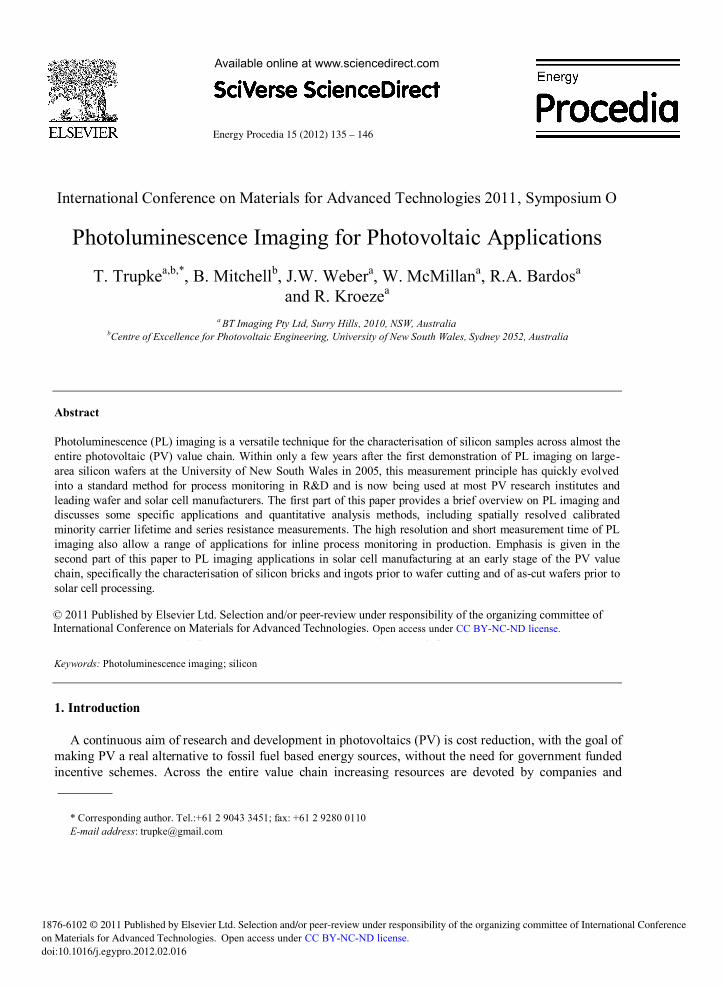
2.1. Minority carrier lifetime imaging
The proportionality of the rate of spontaneous emission to the np product has important implications. In contrast to most other measurement techniques, luminescence measurements are not significantly affected by minority carrier trapping or by artifacts caused by excess carriers accumulated in space charge regions [8, 9]. This is relevant since the minority carrier lifetime is a strong function of the excess carrier density (i.e., of the injection level). Lifetime information that is relevant for the operation of the solar cell should therefore be measured under conditions that are equivalent to the operation conditions of the cell in the sun. Typical industrial solar cells operate at excess carrier densities on the order 1013 to 1014 cm-3. PL allows carrier lifetime measurements at these and much lower excess carrier densities, where other techniques are either not sensitive or affected by the above artifacts. PL imaging was therefore initially proposed and demonstrated as a fast technique to measure the minority carrier lifetime with high spatial resolution [7]. Using PL imaging, effective minority carrier lifetime images on passivated or diffused wafers can be acquired with megapixel resolution within a second or less, orders of magnitude faster than is possible e.g. with microwave photoconductance decay mapping tools that are commonly used for this purpose. An example of a calibrated lifetime image is shown in Fig. 1.
Fig. 1. Effective minority carrier lifetime from a PL image on a 6-inch SiN passivated multicrystalline silicon wafer. Calibration was achieved using a Sinton Instruments WCT120 QSSPC system integrated into the BT Imaging LIS-R1 PL imaging system.

138 T. Trupke et al. / Energy Procedia 15 (2012) 135 – 1464 T. Trupke et al. / Energy Procedia 00 (2011) 000–000
A complication with interpreting PL signal in terms of carrier lifetime arises from the fact that the rate of spontaneous emission rsp and thereby the measured PL signal is not only determined by the excess minority carrier density n, but also by the net background doping ND/A,net:
rsp =Bn(ND/A,net+n) , (1)
with B the radiative recombination coefficient. In addition, the fraction of the rate of spontaneous emission that escapes and can therefore be measured as PL signal also depends strongly on the optical properties of the sample. A separate calibration is therefore required for each distinct type of sample. A number of calibration approaches have been demonstrated in the literature, including correlation of PL imaging data with non-spatially resolved data from quasi steady state photoconductance (QSSPC) [10, 11] or with self consistently calibrated quasi-steady-state photoluminescence [7, 12]. Various variations of so-called dynamic calibration methods, which all rely in one way or the other on a direct or implicit comparison between steady-state and transient measurement conditions, were proposed and demonstrated for both non-spatially resolved PL measurements [13, 14] and for PL images [15, 16]. All these approaches have specific benefits and limitations in terms of their applicability, the latter specifically on samples with low carrier lifetime. Some fundamental limitations of these calibration methods, particularly for poorly passivated samples and for samples with large lateral variations in carrier lifetime, were recently pointed out [17].
The QSSPC technique [18] is well established and represents a benchmark within the PV community for quantitative measurements of the injection level dependent minority carrier lifetime (see e.g. SEMI standard SEMI PV13-0211). Calibration by comparison with QSSPC is therefore the most accurate calibration approach in our view. A Sinton Instruments WCT120 QSSPC system is integrated into the BT Imaging LIS-R1 luminescence imaging tool used for all PL images shown in this paper.
2.2. Series resistance imaging
Both the np-product and the luminescence signal IPL are exponentially related to the diode voltage Vd: IPL~ rsp =Cnp=Cni
2exp(eVd/kT) (2)
with ni is the intrinsic carrier density, rsp the total rate of spontaneous emission across the thickness of the
device, kT the thermal voltage and C a proportionality factor that accounts for the optical properties of the sample. Lateral variations in Vd caused by lateral variations in the series resistance RS under operating conditions that cause current flow into the device or current being extracted from the device can therefore be quantified from luminescence images. First experimental data showing a comparison of a PL image, an EL image and a PL image with current extraction taken on a cell with strong local series resistance variations were presented in [20], suggesting the use of luminescence imaging for spatially resolved series resistance measurements. A quantitative method for measuring the series resistance in units of cm2, based on comparing PL images taken under different illumination and bias conditions was demonstrated shortly thereafter [21]. As in the case of lifetime measurements, the main advantage of the PL imaging approach is measurement speed and spatial resolution. A megapixel image of the series resistance can be measured in a matter of seconds. For comparison Corescan [22], a mapping technique, that specifically measures the front contact resistance between the metal grid and the emitter, is orders of magnitude slower and destructive.
Series resistance information is contained in principle in any luminescence image taken with current
flow over the contacts. A particularly accurate PL-based method allowing very accurate separation of Rs
139T. Trupke et al. / Energy Procedia 15 (2012) 135 – 146 T. Trupke et al. / Energy Procedia 00 (2011) 000–000 5
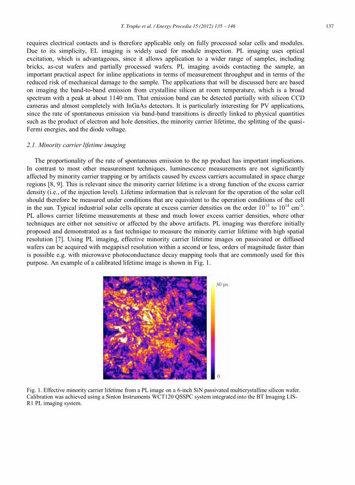
effects from minority carrier lifetime variations was introduced by Kampwerth et al. [19]. The method is implemented in the BT Imaging LIS-R1 tool that was used for the series resistance image of Fig. 2.
Fig. 2. Series resistance image of a multicrystalline Si cell. The color bar represents the series resistance in cm2. The measurement was performed on a BT Imaging LIS-R1, which incorporates the RS analysis presented in [19].
A number of additional luminescence based series resistance imaging techniques have been proposed, including EL based techniques [23-26] and the comparison of luminescence images with lock in thermography data [27]. PL based RS-imaging methods are advantageous compared to EL based methods, primarily since they allow a significantly more accurate separation of series resistance effects from lateral variations in the minority carrier lifetime, and secondly because they allow measuring the series resistance under operating conditions equivalent to the maximum power point. The latter is important point since the series resistance itself depends on the operating point of the solar cell. Given the short measurement times required for luminescence images, inline measurements of the series resistance become feasible. Compared to global RS data, as can be obtained from I-V data, RS images have the advantage, that even subtle variations in RS, that are too small to be identified in global RS measurements, which can however have a noticeable impact on average cell efficiency, can be identified earlier in production. In addition the spatial fingerprint of specific RS problems, such as the belt pattern shown in Fig. 2, often provides easy to interpret clues on the origin of the problem.
2.3. Other applications
A range of other applications have been demonstrated or are under current investigation. EL images with different spectral filters have been used to measure the diffusion length in finished solar cells [28]. The equivalent method was also applied with some success to PL imaging on silicon wafers [29]. An ideal applications of this so-called “PL intensity ratio method” (PLIR) is the measurement of bulk lifetime (or bulk diffusion length) on silicon bricks [30, 31], as discussed in more detail below.
Shunt detection from luminescence images has also been investigated [32-34]. Combining the
localisation of shunts from luminescence images with laser shunt isolation was proposed and demonstrated in [35]. While most work on shunt detection so far has been largely qualitative, progress with a quantitative analysis of luminescence images in terms of shunt currents was reported [36].
140 T. Trupke et al. / Energy Procedia 15 (2012) 135 – 1466 T. Trupke et al. / Energy Procedia 00 (2011) 000–000
The quantitative evaluation of luminescence images in terms of the concentration of specific lifetime limiting impurities is another active field of research. PL images can be used to measure images of the concentration of interstitial iron in boron doped silicon [37], allowing detailed spatial information to be gained about the dynamics of defect formation under specific processing conditions [38]. PL imaging based images of the chromium concentration were also reported [39]. A recent polarisation analysis of luminescence images showed strong correlations with specific structural defects within silicon solar cells such as dislocations [40]. Progress has also been made with the analysis of reverse bias luminescence imaging on solar cells [41, 42].
3. PL imaging on silicon bricks
3.1. Qualitative analysis
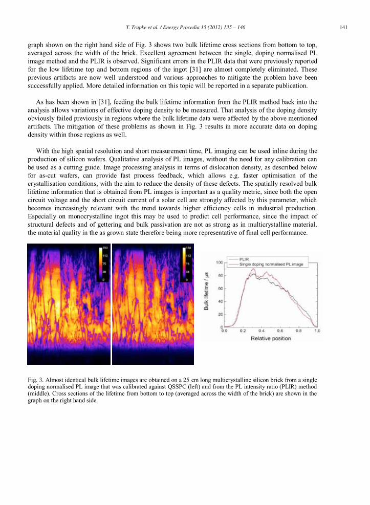
Figure 3 (left) shows a calibrated PL image taken on the side face of a typical 25 cm high 6x6 inch boron doped cast multicrystalline silicon brick prior to wafer slicing (data taken from [31]). Dark bands with strongly reduced PL count rate are seen near the bottom and top of the brick and also near the left hand edge. These bands represent regions that have severely reduced bulk lifetime due to high impurity concentrations (e.g. oxygen, carbon, transition metals), which is a result of diffusion of impurities from the crucible walls into the ingot, segregation from bottom to top during crystallisation and back diffusion from the top during cooling. The image also shows the distribution of efficiency limiting structural defects such as dislocation networks. An area of high dislocation density is seen in the top right hand corner of this brick. These dislocation networks are of particular relevance, since they remain as efficiency limiting defects in the finished cells, as discussed in more detail below.
3.2. Bulk lifetime
The measured PL signal is determined by the effective lifetime eff, which is generally affected by both bulk and surface recombination and which can be expressed in simplified form as:
surfacebulkeff 111
. (3)
Effective lifetime measurements on as as-cut wafers can be strongly affected or completely dominated by the surface recombination component for bulk lifetimes exceeding about 10 s. In contrast, effective lifetimes in a brick show significant variation up to very large bulk lifetime values of several milli-seconds, allowing a transfer function to be calculated that converts measured effective lifetime to bulk lifetime [43-45]. A single PL image can be converted into bulk lifetime using that method (see Fig. 3, left). Complications with that approach are associated with the fact that the variations in effective doping density must be accounted for, which requires a separate doping measurement.
The PL intensity ratio method (PLIR), described in detail in the context of diffusion length imaging on
fully processed silicon solar cells in Ref. [26], is a suitable alternative approach for the calibration of PL images taken on silicon bricks [30, 31], and as a way to avoid the need for a separate doping measurement. With effectively infinite thickness and polished surfaces, silicon bricks are ideal for that method, since inaccuracies that are associated with thickness variations, surface texture and the impact of the rear reflectance are avoided. The key point of the PL intensity ratio method is that variations in background doping density cancel out in the intensity ratio and that no absolute PL intensity is needed. The right hand side of Fig. 3 shows a bulk lifetime image obtained from the PLIR methodology. The
141T. Trupke et al. / Energy Procedia 15 (2012) 135 – 146 T. Trupke et al. / Energy Procedia 00 (2011) 000–000 7
graph shown on the right hand side of Fig. 3 shows two bulk lifetime cross sections from bottom to top, averaged across the width of the brick. Excellent agreement between the single, doping normalised PL image method and the PLIR is observed. Significant errors in the PLIR data that were previously reported for the low lifetime top and bottom regions of the ingot [31] are almost completely eliminated. These previous artifacts are now well understood and various approaches to mitigate the problem have been successfully applied. More detailed information on this topic will be reported in a separate publication.
As has been shown in [31], feeding the bulk lifetime information from the PLIR method back into the
analysis allows variations of effective doping density to be measured. That analysis of the doping density obviously failed previously in regions where the bulk lifetime data were affected by the above mentioned artifacts. The mitigation of these problems as shown in Fig. 3 results in more accurate data on doping density within those regions as well.
With the high spatial resolution and short measurement time, PL imaging can be used inline during the
production of silicon wafers. Qualitative analysis of PL images, without the need for any calibration can be used as a cutting guide. Image processing analysis in terms of dislocation density, as described below for as-cut wafers, can provide fast process feedback, which allows e.g. faster optimisation of the crystallisation conditions, with the aim to reduce the density of these defects. The spatially resolved bulk lifetime information that is obtained from PL images is important as a quality metric, since both the open circuit voltage and the short circuit current of a solar cell are strongly affected by this parameter, which becomes increasingly relevant with the trend towards higher efficiency cells in industrial production. Especially on monocrystalline ingot this may be used to predict cell performance, since the impact of structural defects and of gettering and bulk passivation are not as strong as in multicrystalline material, the material quality in the as grown state therefore being more representative of final cell performance.
Fig. 3. Almost identical bulk lifetime images are obtained on a 25 cm long multicrystalline silicon brick from a single doping normalised PL image that was calibrated against QSSPC (left) and from the PL intensity ratio (PLIR) method (middle). Cross sections of the lifetime from bottom to top (averaged across the width of the brick) are shown in the graph on the right hand side.
142 T. Trupke et al. / Energy Procedia 15 (2012) 135 – 1468 T. Trupke et al. / Energy Procedia 00 (2011) 000–000
4. Quality control on as-cut wafers
4.1. Measuring PL images at line speed
Total recombination (and thus effective lifetime) in as-cut wafers is strongly affected by the surface recombination. Luminescence quantum efficiencies of as-cut wafers are therefore extremely low, typically on the order 10-7-10-8. This makes the complete separation of the PL signal from stray light and other artifacts an experimental challenge and also requires generally longer exposure times. Data acquisition times of 30s to 100s have been reported in the literature. Commercial systems that allow measurement of full megapixel PL images on silicon wafers at line speed have recently been introduced [46]. These tools now allow for the first time inline quality monitoring of as-cut wafers and correlation of defect features with cell performance, as described below.
4.2. Analysing PL images on as cut wafers
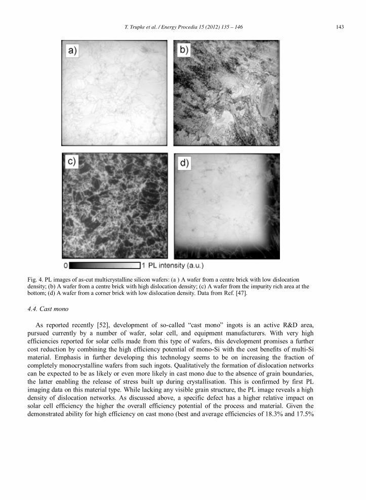
As has been reported previously [47-51] various defect related spatial features are commonly observed in PL images on mc-Si as-cut wafers. Figure 4 shows four typical examples, (a) a wafer from a center brick with low dislocation density, (b) a wafer from a brick cut from the centre of an ingot containing high dislocation density, (c) a wafer from the impurity rich area at the bottom and (d) a wafer from a corner brick with low dislocation density. Image processing can be used to extract quality metrics from PL images on as-cut wafers such as a dislocation area fraction, extension of low-lifetime regions from corner/edge or top/bottom wafers or other crystallisation-induced material defects [48, 49, 51].
4.3. Correlation with cell performance
Previous studies have shown a strong correlation of the dislocation density metrics extracted from PL images taken on as cut wafers with I-V parameters measured on finished cells. An ~8% relative variation in cell efficiency with dislocation density (equivalent to about 1.3% absolute efficiency variation) was reported in [48], a similar strong correlation of cell efficiency with a defect metric obtained from PL images on as-cut wafers was reported recently [51]. Dislocations affect both Isc and Voc. A variation of ~25 mV in Voc with dislocation density was reported in [48], a 5% relative reduction in Isc with increasing dislocation density in [48]. The details of these correlations, i.e. the specific impact of dislocations and other defects on cell performance depends strongly on the cell process, specifically the ability of the process to remove or passivate defects via gettering and hydrogenation. PL imaging offers the unique possibility to obtain the relevant defect information without any sample preparation. Thus, a standardised wafer rating based on PL images can be introduced. Wafer manufacturers can use these metrics to sort wafers into different quality bins. Bin specific extra processing steps, sorting of wafers to high- and low-efficiency processing lines or to specifically tuned production lines, outright rejection of wafers and wafer quality based pricing are some possible outcomes of such wafer quality rating.
High-efficiency cell concepts such as selective emitter structures and cells with rear point contacts,
which will increasingly be adopted in the industry in the next few years, will allow solar cell efficiencies exceeding 18% to be reached on mc-Si wafers. The impact of defects on cell efficiency can be expected to be even higher than the variations discussed above, which were obtained from conventional screen printed cell lines. Another appealing aspect of wafer pre-sorting is that much more efficient statistical process optimisation and fine tuning of production equipment is enabled with pre-sorted wafers, since the substantial variations in cell performance that are caused by the wafer quality can be eliminated.
143T. Trupke et al. / Energy Procedia 15 (2012) 135 – 146 T. Trupke et al. / Energy Procedia 00 (2011) 000–000 9
Fig. 4. PL images of as-cut multicrystalline silicon wafers: (a ) A wafer from a centre brick with low dislocation density; (b) A wafer from a centre brick with high dislocation density; (c) A wafer from the impurity rich area at the bottom; (d) A wafer from a corner brick with low dislocation density. Data from Ref. [47].
4.4. Cast mono
As reported recently [52], development of so-called “cast mono” ingots is an active R&D area, pursued currently by a number of wafer, solar cell, and equipment manufacturers. With very high efficiencies reported for solar cells made from this type of wafers, this development promises a further cost reduction by combining the high efficiency potential of mono-Si with the cost benefits of multi-Si material. Emphasis in further developing this technology seems to be on increasing the fraction of completely monocrystalline wafers from such ingots. Qualitatively the formation of dislocation networks can be expected to be as likely or even more likely in cast mono due to the absence of grain boundaries, the latter enabling the release of stress built up during crystallisation. This is confirmed by first PL imaging data on this material type. While lacking any visible grain structure, the PL image reveals a high density of dislocation networks. As discussed above, a specific defect has a higher relative impact on solar cell efficiency the higher the overall efficiency potential of the process and material. Given the demonstrated ability for high efficiency on cast mono (best and average efficiencies of 18.3% and 17.5%

144 T. Trupke et al. / Energy Procedia 15 (2012) 135 – 14610 T. Trupke et al. / Energy Procedia 00 (2011) 000–000
were reported by JA Solar, even higher average efficiencies of 18.8% by GT Solar [52]), dislocations networks will have an even bigger impact on absolute cell efficiency than reported above for multi-Si wafers. The above 0.8% absolute efficiency spread between best and average efficiency seems to confirm this point. If this type of wafer is adopted by the PV industry in large-scale production, then the need for efficient quality control using PL imaging is even larger than for conventional multi-Si. Process optimisation of the casting process is an immediate application for PL imaging within this context.
Fig. 5. PL image of an as-cut “cast-mono” silicon wafer, measured on a BT Imaging LIS-R1 PL imaging system. The line shaped defects represent areas with high local dislocation density. Previous studies at BT Imaging on cast mono cells indicate that these defects remain recombination active in finished cells and therefore have a strong impact on solar cell efficiency.
5. Summary
The growing pressure in PV production to achieve higher cell efficiencies with high yield and at low cost will result in an increasing need for and adoption of improved quality control and process monitoring tools. With its contactless non-destructive nature, its short measurement time and high repeatability PL Imaging is perfectly suited to be used for such inline monitoring across the entire PV value chain. In this paper we reviewed some specific PL imaging applications to be used both offline in R&D and in-line in production. Particularly promising is the application of PL imaging at an early stage of production. PL imaging on silicon bricks allows early detection of production problems and removal of complete bricks or parts of bricks from further processing. Spatially resolved data on bulk lifetime, impurity rich low lifetime regions and dislocation density are highly relevant parameters that can be extracted from PL images. The data can be correlated with cell performance and can also be used for fast feedback in production on feedstock quality and the impact of processing conditions on the material quality.
PL imaging on as-cut wafers can be used for incoming quality control and wafer sorting by both wafer
and cell makers. It allows the detection of efficiency limiting impure regions near the wafer edges, the identification of top and bottom wafers with low bulk lifetime and the extraction of a dislocation area density, which strongly correlates with final cell performance. The metrics derived from PL images can be used for quality grading and assigning an efficiency entitlement (and thus a “$ value”) to each wafer, which will lead to wafer pricing based on standardised metrics, as done in similar form today in semiconductor manufacturing. Increasing adoption of PL imaging in cell and wafer manufacturing will be a driver for this development.

145T. Trupke et al. / Energy Procedia 15 (2012) 135 – 146 T. Trupke et al. / Energy Procedia 00 (2011) 000–000 11
Acknowledgements
The authors thank Tianwei Solar for providing cast monocrystalline wafers for this study.
References [1] Knoll B. Modules price index. Photon International 2011; 5:124. [2] Würfel P, Finkbeiner S, Daub E. Generalized Planckʼs radiation law for luminescence via indirect transitions. Appl. Phys.
A: Materials Science & Processing 1995; A60:67-70. [3] Schick K, Daub E, Finkbeiner S, Würfel P. Verification of a generalized Planck law for luminescence radiation from
silicon solar cells. Appl. Phys. A: Solids and Surfaces 1992; A54: 109-14. [4] Würfel P. Physik der Solarzellen, Berlin: Spektrum Akademischer Verlag, 2000. [5] Trupke T, Bardos RA, Hudert F, Würfel P, Wang A, Zhao J, Green MA. Effective excess carrier lifetimes exceeding
100ms in float zone silicon determined from photoluminescence. Proc. 19th European Photovoltaic Solar Energy Conf., Paris, France; 2004.
[6] Fuyuki T, Kondo H, Yamazaki T, Takahashi Y, Uraoka Y. Photographic surveying of minority carrier diffusion length in polycrystalline silicon solar cells by electroluminescence. Appl. Phys. Lett. 2005; 86: 262108.
[7] Trupke T, Bardos RA, Schubert MC, Warta W. Photoluminescence imaging of silicon wafers. Appl. Phys. Lett. 2006; 89: 44107.
[8] Bardos RA, Trupke T, Schubert MC, Roth R. Trapping artifacts in quasi-steady-state photoluminescence and photoconductance lifetime measurements on silicon wafers. Appl. Phys. Lett. 2006; 88: 53504.
[9] Trupke T, Bardos R. Photoluminescence: a surprisingly sensitive lifetime technique. Proc. 31st IEEE Photovoltaic Specialists Conf., Orlando, Florida; 2005, p. 903-6.
[10] Trupke T, Bardos RA, Nyhus J. Photoluminescence characterisation of silicon wafers and solar cells. Proc. 18th Workshop on Crystalline Silicon Solar Cells & Modules, Vail, Colorado; 2008.
[11] Herlufsen S, Schmidt J, Hinken D, Bothe K, Brendel R. Photoconductance-calibrated photoluminscence lifetime imaging of crystalline silicon. Phys.Stat.Solidi RRL 2008; 2: 245-7.
[12] Giesecke JA, Warta W, Schubert MC, Michl B, Schindler F. Minority carrier lifetime imaging of silicon wafers calibrated by quasi-steady-state photoluminescence. Sol. Energy Mat. Sol. Cells 2011; 95: 1011-8.
[13] Trupke T, Bardos RA, Abbott MD. Self Consistent Calibration of photoluminescence and photoconductance lifetime measurements. Appl. Phys. Lett. 2005; 87: 184102.
[14] Giesecke JA, Walter D, Kopp F, Rosenits P, Schubert MC, Warta W, Institut F. Simultaneous determination of carrier lifetime and net dopant concentration of silicon wafers from photoluminescence. Proc. 35th IEEE Photovoltaic Specialists Conf., Honolulu, USA; 2010, p. 847-51.
[15] Herlufsen S, Ramspeck K, Hinken D, Schmidt A, Müller J, Bothe K, Schmidt J, Brendel R. Dynamic lifetime imaging based on photoluminescene measurements. Proc. 25th European PV Solar Energy Conf., Valencia, Spain; 2010, p. 2369.
[16] Kiliani D, Micard G, Raabe B, Hahn G. Time resolved photoluminescence imaging for carrier lifetime mapping of silicon wafers. Proc. 25th European Photovoltaic Solar Energy Conf., Valencia, Spain; 2010, p.1363.
[17] Sinton RA, Trupke T. Limitations on dynamic excess carrier lifetime calibration methods. Prog. Photovolt.: 2011; in press. [18] Sinton RA, Cuevas A, Stuckings M. Quasi-steady-state photoconductance, a new method for solar cell material and device
characterisation. Proc. 25th IEEE Photovoltaic Specialists Conf., Washington, USA; 1996, p. 457. [19] Kampwerth H, Trupke T, Weber J, Augarten Y. Advanced luminescence based effective series resistance imaging of
silicon solar cells. Appl. Phys. Lett. 2008; 93: 202102. [20] Trupke T, Bardos RA, Abbott MD, Chen FW, Cotter JE, Lorenz A. Fast photoluminescence imaging of silicon wafers.
Proc. 4th World Conf. on Photovoltaic Energy Conversion, Waikoloa, USA; 2006, p. 928. [21] Trupke T, Pink E, Bardos RA, Abbott MD. Spatially resolved series resistance of silicon solar cells obtained from
luminescence imaging. Appl. Phys. Lett. 2007; 90: 93506. [22] van der Heide ASH, Bultmann JH, Hoornstra J, Schönecker A. Contact resistance measured using the Corescan: relations
with cell processing. Proc. 17th European Photovoltaic Solar Energy Conf., Munich, Germany; 2001, p. 1531. [23] Hinken D, Ramspeck K, Bothe K, Fischer B, Brendel R. Series resistance imaging of solar cells by voltage dependent
electroluminescence. Appl. Phys. Lett. 2007; 91: 182104. [24] Breitenstein O, Khanna A, Augarten Y, Bauer J, Wagner JM, Iwig K. Quantitative evaluation of electro-luminescence
images of solar cells. Phys. Stat.Solidi RRL 2010; 4: 7- 9. [25] Haunschild J, Glatthaar M, Kasemann M, Rein S, Weber ER. Fast series resistance imaging for silicon solar cells using
electroluminescence. Phys. Stat. Solidi RRL 2009; 3; 227-29.

146 T. Trupke et al. / Energy Procedia 15 (2012) 135 – 14612 T. Trupke et al. / Energy Procedia 00 (2011) 000–000
[26] Glatthaar M, Haunschild J, Kasemann M, Giesecke J, Warta W, Rein S. Spatially resolved determination of dark saturation current and series resistance of silicon solar cells. Phys. Stat. Solidi RRL 2010; 4: 13 5.
[27] Ramspeck K, Bothe K, Hinken D, Fischer B, Schmidt J, Brendel R. Recombination current and series resistance imaging of solar cells by combined luminescence and lock-in thermography. Appl. Phys. Lett. 2007; 90: 153502.
[28] Würfel P, Trupke T, Puzzer T, Schäffer E, Warta W, Glunz S. Diffusion lengths of silicon solar cells obtained from luminescence images. J. Appl. Phys. 2007; 101: 123110.
[29] Giesecke JA, Kasemann M, Schubert MC, Würfel P, Warta W. Separation of local bulk and surface recombination in crystalline silicon from luminescence reabsorption. Prog. Photovolt.: Res. Appl. 2009; 18: 10-19.
[30] Trupke T, Mitchell B, Weber JW, Nyhus J. Bulk minority carrier lifeitme from luminescence intensity ratios measured on silicon bricks.Proc. 25th European Photovoltaic Solar Energy Conf., Valencia, Spain; 2010, p. 1307.
[31] Mitchell B, Trupke T, Nyhus J, Weber JW. Bulk minority carrier lifetimes and doping of silicon bricks from photo-luminescence intensity ratios. J. Appl.Phys. 2011; 109: 083111.
[32] Trupke T, Bardos RA, Abbott MD, Fisher K, Bauer J, Breitenstein O. Luminescence imaging for fast shunt localisation in silicon solar cells and silicon wafers. Proc. Internat'l Workshop on Science and Technology of Crystalline Silicon Solar Cells, Sendai, Japan; 2006.
[33] Kasemann M, Grote D, Walter B, Trupke T, Augarten Y, Bardos RA, Pink E, Abbott MD, Warta W. Shunt detection capabilities of luminescence imaging on silicon solar cells. Proc. 22nd European PV Solar Energy Conf., Milan, Italy; 2007.
[34] Breitenstein O, Bauer J, Trupke T, Bardos RA. On the detection of shunts in silicon solar cells by photo- and electro-luminescence imaging. Prog. Photovolt.: Res. Appl. 2008; 16: 325.
[35] Abbott MD, Trupke T, Hartmann HP, Gupta R, Breitenstein O. Laser isolation of shunted regions in industrial soalr cells. Prog. Photovolt.: Res. Appl. 2007; 15: 613.
[36] Augarten Y, Trupke T, Lenio M, Bauer J, Breitenstein O, Weber J, Bardos RA. Luminescence shunt imaging: qualitative and quantitative shunt images using photoluminesccence imaging. Proc. 24th European PV Solar Energy Conf., Hamburg, Germany; 2009, p. 27.
[37] Macdonald D, Tan J, Trupke T. Imaging interstitial iron concentration in boron-doped crystalline silicon using photo-luminescence. J. Appl. Phys. 2008; 103: 73710.
[38] Liu A, Fan YC, Macdonald D. Interstitial iron concentrations across multicrystalline silicon wafers via photoluminescence imaging. Prog. Photovolt.: Res. Appl. 2011; vol. online.
[39] Habenicht H, Schubert MC, Warta W. Imaging of chromium point defects in p-type silicon. J. Appl. Phys. 2010; 034909. [40] Peloso MP, Hoex B, Aberle AG. Polarization analysis of luminescene for the characterization of silicon wafer solar cells.
Appl. Phys. Lett. 2011; 98: 171914. [41] Lausch D, Petter K, von Wenckstern H, Grundmann M. Correlation of pre-breakdown sites and bulk defects in
multicrystalline silicon solar cells. Phys. Stat. Solidi RRL 2009; 3: 702. [42] Schneemann M, Helbig A, Kirchartz T, Carius R, Rau U. Reverse biased electroluminescence spectroscopy of crystalline
silicon solar cells with high spatial resolution. phys. stat. solidi (a) 2010; 207: 2597. [43] Bowden S, Sinton RA. Determining lifetime in silicon blocks and wafers with accurate expressions for carrier density. J.
Appl. Phys. 2007; 102: 124501. [44] Swirhun JS, Sinton RA, Forsyth MK, Mankad T. Contactless measurement of minority carrier lifetime in silicon ingots and
bricks. Prog. Photovolt.: Res. Appl. 2011; 19: 313-19. [45] Trupke T, Nyhus J, Sinton RA, Weber J. Photoluminescence imaging on silicon bricks. Proc. 24th European Photovoltaic
Solar Energy Conf., Hamburg, Germany; 2009, p. 1029. [46] Chunduri SK. No Place to hide - market survey on luminescence imaging systems and cameras. Photon International 2011;
1: 158. [47] Trupke T, Nyhus J, Haunschild J. Luminescence imaging for inline characterisation in silicon photovoltaics. Phys. Stat.
Solidi RRL 2011; 5: 131-37. [48] McMillan W, Trupke T, Weber J, Wagner M, Mareck U, Chou YC, Wong J. In-line monitoring of electrical wafer quality
using photoluminescence imaging. Proc. 25th European Photovoltaic Solar Energy Conf., Valencia, Spain; 2010, p. 1347. [49] Haunschild J, Glatthaar M, Demant M, Nievendick J, Motzko M, Rein S, Weber E. Quality control of as-cut multicrystal-
line silicon wafers using photoluminescene imaging for solar cell production. Sol. En. Mat. Sol. Cells 2010; 94: 2007-2012. [50] Demant M, Glatthaar M, Haunschild J, Rein S. Analysis of luminescence images applying pattern recognition techniques.
Proc. 25th European Photovoltaic Solar Energy Conf., Valencia, Spain; 2010, p. 1078. [51] Johnston S, Yan FY, Zaunbrecher K, Al-jassim M, Sidelkheir O, Blosse A. Imaging study of multi-crystalline silicon
wafers throughout the manufacturing process. Proc. 37th IEEE Photovoltaic Specialists Conf., Seattle, USA; 2011. [52] Chunduri SK. The quest for quasi. Photon International - The Solar Power Magazine 2011; 6: 260.