Overview of Lithography: Challenges and Metrologies Harry J
40
Overview of Lithography: Challenges and Metrologies Harry J. Levinson
Transcript of Overview of Lithography: Challenges and Metrologies Harry J

Overview of Lithography: Challenges and Metrologies
Harry J. Levinson

4/3/2003 Harry J. Levinson 2
Progress in Lithography
•Progress in lithography has been the result of many advances.
–Better lenses, resists, chemical-mechanical polishing (CMP), etc.
•The largest impacts have been made by changes in wavelength.
g-line → i-line → KrF → ArF → F2
436 nm → 365 nm → 248 nm → 193 nm → 157 nm
1 µm 360 nm

4/3/2003 Harry J. Levinson 3
Shorter wavelengths
•Shorter wavelengths make a number of problems easier.
–Improved depth-of-focus.
–Smaller mask error factor.
–Larger image log-slope.
•Improves exposure latitude, sensitivity to resist thickness, and increases resist side-wall slope.
•We are running out of wavelengths.

4/3/2003 Harry J. Levinson 4
Why are we running out of wavelengths?
•Optical lithography is defined as a lithographic technology that:
–Uses photons to induce chemical reactions in a photoresist.
–Has the potential for image reduction using projection optics.
–Involves a transmission photomask.

4/3/2003 Harry J. Levinson 5
Why are we running out of wavelengths?
•Optical lithography is defined as a lithographic technology that:
–Uses photons to induce chemical reactions in a photoresist.
–Has the potential for image reduction using projection optics.
–Involves a transmission photomask.
No solution is apparent for wavelengths < 157 nm.

4/3/2003 Harry J. Levinson 6
What goes wrong at λ < 157 nm?
•Photomasks today are made from fused silica.
•Fused silica has a number of advantageous properties.
–Chemical stability.
–Transparency for ultraviolet light.
–No intrinsic birefringence.
–A low coefficient of thermal expansion.

4/3/2003 Harry J. Levinson 7
What goes wrong at λ < 157 nm?
•A low coefficient of thermal expansion.
•0.5 ppm/oC.
–If a mask changes temperature by 0.1oC, then the distance between two features separated by 50 mm will change by 2.5 nm.
–This change in registration can be absorbed into overlay budgets.
•After reduction by 4×.
Year of Production 2010 2013 2016DRAM ½ Pitch (nm) = node 45 32 22Overlay 18 13 9

4/3/2003 Harry J. Levinson 8
What goes wrong at λ < 157 nm?
•The transparency of fused silica must be modified by fluorine doping to have adequate transparency for use as substrates for photomasks at 157 nm.
–The transmission falls off sharply for smaller wavelengths.
•An alternative material must be used.
–CaF2.
• The coefficient of thermal expansion of CaF2 is 19 ppm/oC.
–Versus 0.5 ppm/oC for fused silica.
•The 2.5 nm of mask registration error becomes nearly 50 nm.

4/3/2003 Harry J. Levinson 9
What goes wrong at λ < 157 nm?
There will be no optical lithography for wavelengths
< 157 nm.
(Maybe. More later.)

4/3/2003 Harry J. Levinson 10
What are our choices?
•We will need to operate very close to the resolution limit of the optics.
or
•We need to adopt a radically new approach to lithography.
•Either of these will be hard to do.

4/3/2003 Harry J. Levinson 11
International Technology Roadmap for Semiconductors (ITRS)
I will talk about three of the most difficult challenges going forward in lithography:
–Gate CD control.
–The introduction of completely new lithographic technologies.
•Extreme Ultraviolet (EUV) lithography, for example.
–The escalating costs of lithography.

4/3/2003 Harry J. Levinson 12
What will be the hardest problems?
•As one looks at the ITRS today, the biggest lithographychallenges involve critical dimension (CD) control.
–Particularly for microprocessors.
2002 2003 2004 2005 2006 2007115 nm 100 nm 90 nm 80 nm 70 nm 65 nm
Gate length (nm, in resist) 75 65 53 45 40 35
Gate length (nm, post-etch) (physical length)
53 45 37 32 28 25
Gate CD control (nm, 3 sigma, post-etch, 10% of CD, litho only)
4.3 3.7 3.0 2.6 2.3 2.0
Year of Production
MPU/ASIC

4/3/2003 Harry J. Levinson 13
What will be the hardest problems?
95 0397 0199 05 07 09 11 13
Year
Fina
l gat
e di
men
sion
(nm
)
100705035251813
1994
2001
9 year acceleration!
500350250180130

4/3/2003 Harry J. Levinson 14
What will be the hardest problems?
•CD variation results from a number of factors.
–Reticles.
–Exposure tools.
•Stepper lenses.
•Focus variation.
•Dose control.
–Resist processing.
•Bakes, for example.
–Line-edge roughness (LER).
–Metrology.

4/3/2003 Harry J. Levinson 15
What will be the hardest problems?

4/3/2003 Harry J. Levinson 16
What will be the hardest problems?
•Suppose metrology accuracy needs to be 10% of requirements.
2002 2003 2004 2005 2006 2007115 nm 100 nm 90 nm 80 nm 70 nm 65 nm
Gate length (nm, post-etch) (physical length)
53 45 37 32 28 25
Gate CD control (nm, 3 sigma, post-etch, 10% of CD, litho only)
4.3 3.7 3.0 2.6 2.3 2.0
Metrology accuracy (nm, 3 sigma) 0.43 0.37 0.30 0.26 0.23 0.20
Year of Production
•Improvement will require attention to contributions that are a fraction of the total requirement.
–Metrology will need to be capable of dealing with individual contributions.

4/3/2003 Harry J. Levinson 17
What will be the hardest problems?
•Fortunately, we do not always need to measure resist features or CDs directly on the wafer to prove to ourselves that things have been improved.
–Reticles can be measured at 4×.
–Hotplates temperatures can be measured.
–Lens aberrations can be measured by interferometry.
•It will still be hard!
4/3/2003 Harry J. Levinson 18
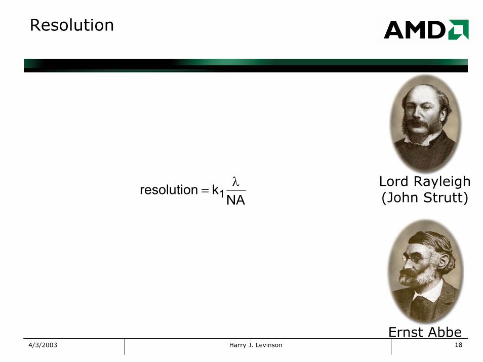
Resolution
Lord Rayleigh(John Strutt)NA
kresolution 1λ
=
Ernst Abbe
4/3/2003 Harry J. Levinson 19
What will be the hardest problems?
•As we make features smaller, everything must be controlled better.
–This becomes increasingly difficult the smaller k1 becomes.
•We are reaching practical limits.
•We are also reaching physical limits.

4/3/2003 Harry J. Levinson 20
How far can optical lithography go?
NAkresolution 1
λ=
≥ 0.25
≥ 157 nm
?

4/3/2003 Harry J. Levinson 21
Resolution
Lord Rayleigh(John Strutt)
NAkresolution 1
λ=
Ernst Abbe
2θ
aperture
bottom lens elements
exposure field
NA = n sinθ

4/3/2003 Harry J. Levinson 22
Immersion lithography
•One way to increase the numerical aperture is to employ immersion imaging.
lens
wafer
•Immersion can potentially enable NA > 1.
–This technology will have its own challenges.

4/3/2003 Harry J. Levinson 23
Immersion lithography
•Immersion lithography challenges:
–Moving wafers in and out of the fluid.
–Scanning.
–Bubbles.
–Immersion fluid transparency at 157 nm.
•Work on this has begun only recently.
–Time and money are needed for proof-of-principle and development.

4/3/2003 Harry J. Levinson 24
What is the resolution limit of immersionlithography?
NAkresolution 1
λ=
• Assume
• k1 > 0.25 theoretically, but k1 ≥ 0.3 is more realistic.
• λ = 157 nm
• NA = 1.3
• Resolution of optical immersion lithography > 36 nm.

4/3/2003 Harry J. Levinson 25
Next Generation Lithography
•To overcome the limits of optical lithography, a different approach to lithography will be required.
–EUV lithography.
–Electron projection lithography (EPL).
–Maskless lithography
•Any one of these will require significant advances in exposure tools, resists, masks (except maskless) and metrology.
•We have invested 25 years in learning about projection optics, optical resists, and optical masks.
•With a change in technology type, we need to start over.

4/3/2003 Harry J. Levinson 26
EUV Lithography
•EUV lithography involves reflection optics and masks.
NA = 0.14λ = 13.4 nm
M1 M2
M3
M4
Mask
Wafer

4/3/2003 Harry J. Levinson 27
EUV Lithography
•High reflectivity is achieved through the use of multi-layer Bragg reflectors.
Absorber
Multilayer reflector

4/3/2003 Harry J. Levinson 28
EUV Lithography
•Multilayers will need to have well controlled peak wavelengths.
New metrology capabilities will be required.

4/3/2003 Harry J. Levinson 29
EUV Lithography
•Mask flatness is required well beyond anything required currently.
Spec for flatness = 45 nm P-V at the 32 nm node.

4/3/2003 Harry J. Levinson 30
EUV Lithography
For EUV (λ = 13.4 nm),33 Å =180o out of phase
Multilayer reflector
Absorber
How do we detect this?

4/3/2003 Harry J. Levinson 31
EUV Lithography
•Examples of new metrology capabilities required for EUV lithography.
–Flatness measurements for masks.
•10’s of nanometers of accuracy.
–Reflectance at EUV wavelengths.
–Mask defect detection.
•< 50 nm in width and only a few nm high.
–Surface roughness < 1 nm (rms).

4/3/2003 Harry J. Levinson 32
The next big step lithography
•There are a number of options for the next step in lithographic technology.–EUV Lithography.–Electron Projection Lithography.–Maskless lithography.
•All of these require major advances in technology.–Tools.•Light sources.
–Resists.–Masks.–Process control.
•Major advances are hard to do.

4/3/2003 Harry J. Levinson 33
Lithography costs
$0
$10,000,000
$20,000,000
$30,000,000
$40,000,000
$50,000,000
1980 1985 1990 1995 2000 2005Year
Expo
sure
tool
pric
e
Historical tool prices

4/3/2003 Harry J. Levinson 34
Lithography costs
$0
$10,000,000
$20,000,000
$30,000,000
$40,000,000
$50,000,000
1980 1985 1990 1995 2000 2005Year
Expo
sure
tool
pric
e
Historical tool prices

4/3/2003 Harry J. Levinson 35
Lithography costs
0
2
4
6
8
10
1980 1990 2000 2010 2020Year
Tool
pric
e/si
licon
are
a/hr
(arb
. uni
ts)
lower is better

4/3/2003 Harry J. Levinson 36
Lithography costs
0
2
4
6
8
10
1980 1990 2000 2010 2020Year
Tool
pric
e/si
licon
are
a/hr
(arb
. uni
ts)
lower is better

4/3/2003 Harry J. Levinson 37
Lithography costs
•The problem may not be just which lithographic technology is cheaper.
•The problem may turn out to be:
What lithographic technology will enable the semiconductor industry to continue to produce higher performance PCs for less than $1000?

4/3/2003 Harry J. Levinson 38
How do we pay for the R&D?
• The semiconductor industry made money when there were three years between nodes.
• I have seen no economic analysis that says two years per node maximizes profits for our industry.
• The worst downturn in the history of our industry has occured with a two year/mode pace.
• I do not think that one year per node is the answer.
• Innovation is needed.
• Slow down and think!

4/3/2003 Harry J. Levinson 39
Summary
•The end of optical lithography is finally approaching.
–But not immediately!
•Introducing new lithographic technologies will be hard and expensive.
•The speed at which the semiconductor industry travels over the roadmap will slow down.

4/3/2003 Harry J. Levinson 40
Trademark Attribution
AMD, the AMD Arrow logo and combinations thereof are trademarks of Advanced Micro Devices, Inc. Other product names used in this presentation are for identification purposes only and may be trademarks of their respective companies.