Outsourced CMP for Accelerated Process Development · Why Outsource CMP? • Faster Execution - Tap...
30
Semi Semi - - ECS Technical Symposium ECS Technical Symposium - - March 2005 March 2005 Outsourced CMP for Accelerated Process Development by Robert L. Rhoades, Ph.D. Presented to Semi-ECS Technical Symposium Shanghai, China March 2005
Transcript of Outsourced CMP for Accelerated Process Development · Why Outsource CMP? • Faster Execution - Tap...

SemiSemi--ECS Technical Symposium ECS Technical Symposium -- March 2005March 2005
Outsourced CMP for Accelerated Process Development
by
Robert L. Rhoades, Ph.D.
Presented to Semi-ECS Technical SymposiumShanghai, China
March 2005

SemiSemi--ECS Technical Symposium ECS Technical Symposium -- March 2005March 2005
Outline
• Why Outsource CMP?- Background- Expanding applications- Economic drivers
• CMP Process Development- Internal vs outsourced development- Technology issues and financial impact- Examples
• Comments and conclusions

SemiSemi--ECS Technical Symposium ECS Technical Symposium -- March 2005March 2005
Background
• CMP is now recognized a necessary process for most advanced IC process flows.
- Initially guarded as trade secret, now a mainstream process- Still high cost and long implementation time- Requires extensive process and integration expertise- Mainstream on oxide, W, STI, Cu … others in development- Critical to achieving acceptable yield on many device flows
• Many other applications are also in development to leverage CMP for applications beyond traditional CMOS integrated circuits.
SemiSemi--ECS Technical Symposium ECS Technical Symposium -- March 2005March 2005
Who Needs CMP?
CMP
Packaging
ICs
EmergingDevices
Photonics
SpecialtySubstrates
CMPConsumables
MEMS

SemiSemi--ECS Technical Symposium ECS Technical Symposium -- March 2005March 2005
IC Economics: Yield and Die Output
NOTE: Chart is conservative in estimations as many use CMP at or below 0.5 µm due to dramatic yield improvement
Drive to increase output per wafer device & geometry shrinks more CMP
• Higher device output per wafer result from feature size shrinks utilizing CMP
• CMP also significantly increases electrical device yields per wafer
• Competition compels manufacturers to reduce unit costs by utilizing CMP on an increasing percentage of wafer starts

SemiSemi--ECS Technical Symposium ECS Technical Symposium -- March 2005March 2005
New Materials Drive Expansion of CMP
Source: Cabot Microelectronics Corporation
• Chip designers are continually exploring the use of new materials to increase performance, lower power consumption, etc.
• Manufacturing chips with these materials requires new complex CMP processing step.
New materials new manufacturing requirements new polish steps more CMP

SemiSemi--ECS Technical Symposium ECS Technical Symposium -- March 2005March 2005
CMP Process Complexity
• Wafer Parameters- Size / Shape / Flatness- Film Stack Composition
» Metals (Al, Cu, W, Pt, etc.)» Oxide (TEOS, PSG, BPSG, etc.)» Other (polysilicon, low-k polymers, etc.)
- Film Quality Issues» Stress (compressive or tensile)» Inclusions and other defects» Doping or contaminant levels
- Final Surface Requirements» Ultralow surface roughness» Extreme planarization, esp. Copper» Low defectivity at <0.12 um defect size
• Pad Issues- Appropriate materials selection (polyurethane, felt, foam,
etc.)- Conditioning method often not optimal- Lot-to-lot inconsistency from suppliers
• Slurry Issues- Chemistry optimization often required- Mixing and associated inconsistency- Shelf life and pot life sometimes very short- Slurry distribution system (design, cost, upkeep)
» Agglomeration and gel formation» Filtration is often required
- Cleaning method specific to slurry and film- Waste disposal and local regulations
Few companies can afford the luxury of in-house expertise required to address the increasing complexity of CMP processes
• Process Issues- Long list of significant input variables
» Downforce (polish and conditioning)» Platen speed» Carrier speed» Slurry flow» Conditioning method
‧ Disk used (material, diamond size, spacing, etc)‧ Force‧ Speed‧ Sweep profile
- Highly sensitive to local pattern variation- Must maintain consistency at high throughput- Must optimize for variation of incoming films
• Integration Issues- Materials Compatibility
» Electrochemical interactions with two or more metals» Film integrity and delamination, esp. low-k» Film stack compressibility
- Interactions with adjacent process modules» Photolithography» Metal deposition and metal etch» Dielectric deposition and etch
- Electrical design interactions» Feature size constraints» Interactions with local pattern density» Line resistance variation, esp. damascene copper» Dielectric thickness variation » Contact resistance variation

SemiSemi--ECS Technical Symposium ECS Technical Symposium -- March 2005March 2005
Pieces of the Development Puzzle
Expertise:- Highly trained and experienced
technical staff- Understanding of materials science,
chemistry, tribology, and more- Support staff for infrastructure,
maintenance, etc.
Equipment:- Major capital investment- Process tools: Polisher & Cleaner- Metrology: film thickness, defect
inspection, surface topography, etc.- Ongoing expense to maintain
Cleanroom:- Minimum of Class 100, preferably
Class 10 or Class 1- Required support systems include:
DI water, compressed air, wastewater treatment, nitrogen, etc.
- Substantial overhead cost evenwhen idle or unused
Consumables and Test Wafers:- New materials require new slurries- Pad optimization can be difficult- Requires in-depth expertise- Access to large supply base is
extremely helpful in early testing
SemiSemi--ECS Technical Symposium ECS Technical Symposium -- March 2005March 2005
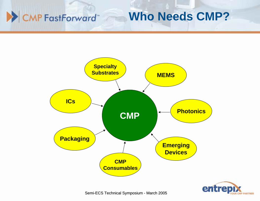
Why Outsource CMP?
• Faster Execution- Tap into existing facility, equipment, and process technology- Reduce implementation time by 12 months or more
• Lower Risk- Leverage technical expertise and known baseline processes
• Lower Cost- Zero capital required- Low unit costs even for low to moderate volume production

SemiSemi--ECS Technical Symposium ECS Technical Symposium -- March 2005March 2005
Typical Internal CMP Development Project
Internal Development:• Project Team:
- Project manager, several members of technical staff from Process, Equipment and Facilities Engineering,
- Most companies then supplement with outside construction contractors- Ongoing staff required for daily operation, maintenance, etc.
• Capital investment:- Equipment:
» CMP, post-CMP Clean, and Metrology- Facilities:
» Site prep, Isolation, Slurry Distribution, DI water, Waste Treatment, Compressed Air, Process Vacuum, and possibly Emissions Control.
• Timing: - Minimum project timing of 12 to 18 months after decision to commit and
funding available- May encounter construction or startup delays if issues with local
permits

SemiSemi--ECS Technical Symposium ECS Technical Symposium -- March 2005March 2005
Typical Outsourced Development Project
Outsourced Development:• Project Team:
- Typically one technologist (may include more if desired)- Outsource staff provide technical consulting throughout the project- Outsource staff maintain the facility and the equipment- Leverages access to advanced processes and expertise
• Capital investment:- Zero: Eliminates capital investment for equipment and facilities
• Timing: - Available immediately

SemiSemi--ECS Technical Symposium ECS Technical Symposium -- March 2005March 2005
CMP Development Project Comparison
Typical Internal Development Lab Project:
Begin
Install and Startup
Lab Design & Layout
Typical Development Project with TFS:
Go
3 mos 6 mos 9 mos 12 mos 15 mos 18 mos
Time
Total Time Savings: 12 months or more
Construction & Equipment Purchase
Internal Development:• Capital Invest: $ 1.5 M• Several Engrs + Staff: $ 1.0 M/Yr• Time to Develop: 18-24 mo.• Multiple learning cycles
Outsourced Development:• Capital Invest: $ 0• One Sr. Engineer: $150K/Yr• Time to Develop: 6-9 mo.• Leverage existing processes, staff,
experience, and consulting
Time to Implement:

SemiSemi--ECS Technical Symposium ECS Technical Symposium -- March 2005March 2005
Bottom Line
As shown in the previous comparisons, outsourcedCMP development accomplishes the following:
1. Simplifies the internal project team (saves headcount)and leverages the expertise of the provider.
2. Substantially shortens the timeline for projectexecution, especially for those who are new to CMPor for fabs that are looking at adding polishers.
3. Zero capital outlay which allows the customer to buyonly tool time necessary to execute each project(avoids adding excess capacity).

SemiSemi--ECS Technical Symposium ECS Technical Symposium -- March 2005March 2005
Outsourced Development Projects:
• Consumables Development- Technology issues and financial impact- Example customer: psiloQuest, Inc.* (CMP pad supplier)
• Integration and Device Qualification- Technology issues and financial impact- Example customer: Medtronics, Inc.* (Medical device supplier)
* Company names used with permission. All other names of Entrepix customers are withheld.

SemiSemi--ECS Technical Symposium ECS Technical Symposium -- March 2005March 2005
Consumables Developer:
• psiloQuest, Inc.- CMP pad supplier trying to penetrate mainstream market- Previously invested in their own internal apps lab- Needed additional capability, esp. for cleans and defectivity
• Results- Improved product characterization (verified by customers)- Through joint efforts, pad was qualified for use with 3rd party
mainstream production wafers- Recent decision to shut down internal lab and outsource all
applications work through Entrepix

SemiSemi--ECS Technical Symposium ECS Technical Symposium -- March 2005March 2005
psiloQuest Tungsten Baseline Data
1000
2000
3000
4000
5000
6000
Start 5 10 15 20 25 30 35 40 45 50
Rem
oval
Rat
e (A
ng/m
in)
0%
5%
10%
15%
20%
25%
Uni
form
ity (%
1-s
igm
a)
Date: March 2004Polisher: IPEC 472Pad: psiloQuestSlurry: Cabot SSW-2000 (diluted 1:1 + 4% H2O2)Conditioning: None
Note: Rate offset due to difference in test wafer lots

SemiSemi--ECS Technical Symposium ECS Technical Symposium -- March 2005March 2005
CMP Integration and Qual:
• Typical needs for CMP integration and qual:- Technical inputs into composition and thickness of layers- Feedback to design team on CMP module sensitivities- Guidance on consumables choices- Starting point CMP processes- Short process runs for prototype devices- Honest technical feedback from an independent perspective- Optimized CMP processes with ability to ramp when needed
All of these can be obtained from aproperly equipped CMP outsource provider

SemiSemi--ECS Technical Symposium ECS Technical Symposium -- March 2005March 2005
CMP Integrationand Qual of New Users
Typical Internal Integration Project (first pass):
Typical Integration Project with TFS:
RampQual.
Develop.
3 mos 6 mos 9 mos 12 mos 15 mos 18 mos 21 mos 24 mos 27 mos 30 mos
Qual.Prod. Ramp
Proj
ect P
hase
s
Time
Total Time Savings: 12-24+ months
Equip. PurchaseDelivery & Qual.
Development
Internal:• Capital Investment: $2.2-3.3M• Multiple Engrs + Staff: $ 1.0 M/Yr• Time to Develop: 18-24 mo.• Multiple learning cycles
Outsourced:• Capital Investment: $ 0• One Sr. Engineer: $150K/Yr• Time to Develop: 6-9 mo.• Leverage existing processes, staff,
experience, and consulting to reduce risk and learning cycles.Time to Implement:

SemiSemi--ECS Technical Symposium ECS Technical Symposium -- March 2005March 2005
CMP Integration and Qual:
• Medtronics, Inc.- Small production fab for medical devices- Unique device integration, including thin CrSi resistor layer- Running 0.6-0.8 um and desires to shrink to 0.35 um- Extreme focus on reliability
• Results- Straight to 3-level CMP integration with both ILD and W CMP- Debugged on existing mask set using < 50 product wafers- Less than 8 months total from concept to first silicon out- First lot to reach probe floor yielded working devices- Design team now working on new masks and qual plans

SemiSemi--ECS Technical Symposium ECS Technical Symposium -- March 2005March 2005
Integration: Reflow BPSG Contact
• BPSG Reflow- Smooth step but not
planar
• Hot Metal Dep.- Acceptable metal
step coverage at 50%
• SOG Gap Fill- Acceptable planar
surface, but not good enough to shrink
SemiSemi--ECS Technical Symposium ECS Technical Symposium -- March 2005March 2005
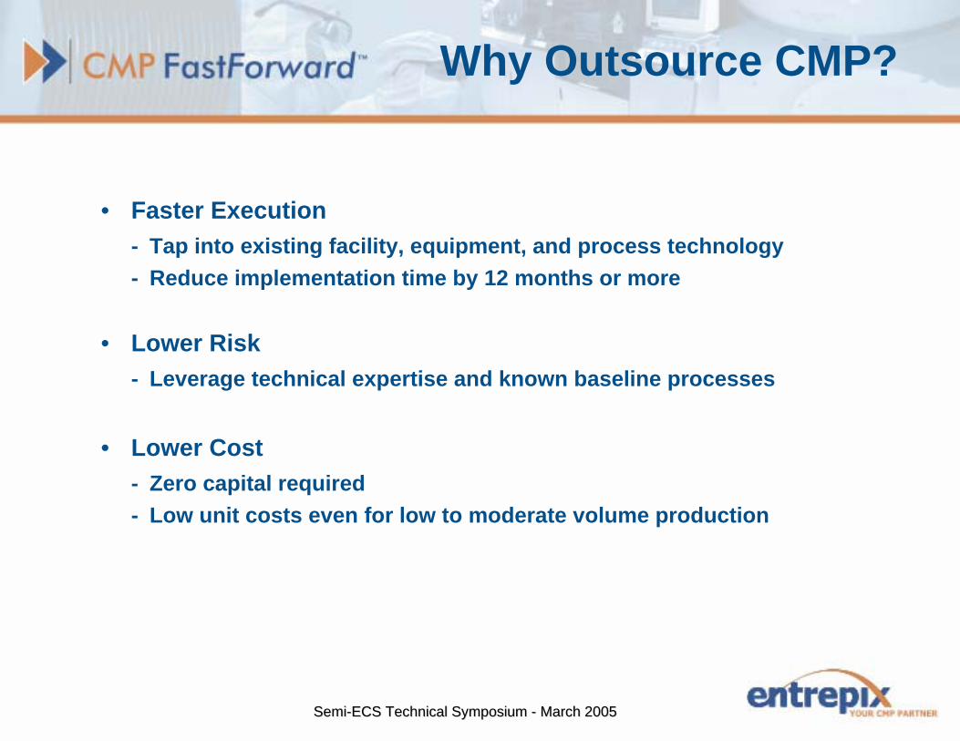
Integration: CMP Planarized Contact
• Good Contact to Substrate
• Ultra Flat BPSG- Photolithography is
improved.- Planarization is
improvedTung sten
Plug
Me tal 1
BPSG
Me tal 1 Co ntact t o Silico n
Titan ium TiWARCL ayer
TEOS T iNBar rier

SemiSemi--ECS Technical Symposium ECS Technical Symposium -- March 2005March 2005
Integration: Non-planarized M1-M2
• Thinning over step.- Less than 20% coverage
on corners
• Poor ILD Planarization.- Has negative impact for
photolithography.- Limits design flexibility.

SemiSemi--ECS Technical Symposium ECS Technical Symposium -- March 2005March 2005
Integration: CMP Planarized M1-M2
• Step coverage no longer an issue.
• Ultra flat surface.- Enhances
photolithography.- More flexibility in
design.

SemiSemi--ECS Technical Symposium ECS Technical Symposium -- March 2005March 2005
Cost Per Wafer comparison:
$-
$500.00
$1,000.00
$1,500.00
$2,000.00
$2,500.00
$3,000.00
$3,500.00
10 15 20 25 35 50 75 100
150
200
250
300
350
400
450
500
550
600
650
700
800
900
1000
1250
1500
1750
2000
Wafers
$ pe
r w
afer
Internal Cost/wfr
TFS Cost/wfr
Total Fab Solutions CONFIDENTIAL Oct. 20
Bottom Line: Low volume cost differential is enormousHigh volume cost differential is minimal
SemiSemi--ECS Technical Symposium ECS Technical Symposium -- March 2005March 2005
Impact of Development Cycles
• Internal development requires additional investments for each node :- Dedicated development teams for each node- Increasing investment in new equipment and facilites dedicated to
new materials: Oxide, W, STI, Cu…
Or...
• Outsourcing development leverages processes and integration expertise of the outsource provider:- Reduces time to qualify new process by 6-18 months- Eliminates capital investment- Reduces risks by using proven solutions

SemiSemi--ECS Technical Symposium ECS Technical Symposium -- March 2005March 2005
Impact of Repeated Development Cycles
NodeKey
Technology
45 nm High-K, Ir & Pt,...
65 nm Cu CMP w/UL-k
90 nm Cu CMP w/CDO or Low-k
130 nm Cu w/ FSG
180 nm STI/ PMD/ Cu CMP
0.25 um W-CMP
0.35 um TEOS-CMP
0.5 um Lmt'd Oxide & W-CMP
0.8 um Pre-CMP
Legend:Prototype
DevelopmentQualificationProd. Ramp
Minim
um Fea
ture Size
Time
Potential Time Savings of 3-6 months per Node using
Outsourced CMP Development

SemiSemi--ECS Technical Symposium ECS Technical Symposium -- March 2005March 2005
Available Outsourced CMP Processes
* Other sizes (2", 3", etc.) and custom shapes can be accommodated with advanced notice
Custom bulk materials
Custom thin films
Backside stress relief polish
N/ASilicon Carbide, Sapphire, DLC
Si, Ge, and various III-V materials
Polysilicon
Copper
Tungsten
Shallow Trench CMP
Doped Oxide (PSG, BPSG, etc.)
Oxide (TEOS, thermal, LTO, etc.)
100 mm125 mm150 mm200 mmProven Processes

SemiSemi--ECS Technical Symposium ECS Technical Symposium -- March 2005March 2005
Summary: Reasons to outsource CMP
• Lower Risk- Immediate access to proven process technology and expertise- Minimize complexity associated with polishers, cleaners,
chemical delivery, filtration, metrology, consumables, etc.• Faster Execution
- Rapid prototyping, development projects or process qualification
- Reduce implementation time an average of 12 to 18 months• Substantial Cost Benefits
- Reduce or eliminate capital expenditures- Lower unit costs
• Production Impact- Perform engineering trials without taking your polishers off line- Flexible manufacturing capacity when you need it
SemiSemi--ECS Technical Symposium ECS Technical Symposium -- March 2005March 2005
Acknowledgements
• Entire staff at Entrepix, with specific thanks to the following individuals:- Jeanie Simmons- Patrick Grimes- Donna Grannis- Terry Pfau- Michael Leone- Mike Bowman- Roy McCoy- Jim Dekarske- Tim Knippa
• psiloQuest, Inc.- Tony Clark, Ed Atkinson,
John Bare, and Dan Marks
• Medtronics, Inc.- Ralph Danzl
• Many other customers who, though unnamed here, have helped us prove that CMP outsourcing is a viable and cost-effective business model.

SemiSemi--ECS Technical Symposium ECS Technical Symposium -- March 2005March 2005
Contact Information
Bob TuckerVice President & General Manager
Tel: 602 426-8675Fax: 602 426-8678
Rob RhoadesChief Technology Officer
Tel: 602 426-8668Fax: 602 426-8678