
Optimization of low temperature GaN buffer layers for ...
21
Optimization of low temperature GaN buffer layers for halide vapor phase epitaxy growth of bulk GaN Carl Hemmingsson and Galia Pozina Linköping University Post Print N.B.: When citing this work, cite the original article. Original Publication: Carl Hemmingsson and Galia Pozina, Optimization of low temperature GaN buffer layers for halide vapor phase epitaxy growth of bulk GaN, 2013, Journal of Crystal Growth, (366), 61- 66. http://dx.doi.org/10.1016/j.jcrysgro.2012.12.016 Copyright: Elsevier http://www.elsevier.com/ Postprint available at: Linköping University Electronic Press http://urn.kb.se/resolve?urn=urn:nbn:se:liu:diva-90144
Transcript of Optimization of low temperature GaN buffer layers for ...

Optimization of low temperature GaN buffer
layers for halide vapor phase epitaxy growth of
bulk GaN
Carl Hemmingsson and Galia Pozina
Linköping University Post Print
N.B.: When citing this work, cite the original article.
Original Publication:
Carl Hemmingsson and Galia Pozina, Optimization of low temperature GaN buffer layers for
halide vapor phase epitaxy growth of bulk GaN, 2013, Journal of Crystal Growth, (366), 61-
66.
http://dx.doi.org/10.1016/j.jcrysgro.2012.12.016
Copyright: Elsevier
http://www.elsevier.com/
Postprint available at: Linköping University Electronic Press
http://urn.kb.se/resolve?urn=urn:nbn:se:liu:diva-90144

1
Optimization of low temperature GaN buffer layers for halide vapour phase
epitaxy growth of bulk GaN
Carl Hemmingsson and Galia Pozina
Department of Physics, Chemistry and Biology (IFM), Linköping University, S-581 83
Linköping, Sweden
Corresponding author: Carl Hemmingsson
Phone: +46 13 282627
Mobile: +46 73 0651264
Fax: +46 13 142337
Email: [email protected]
Abstract
We have studied growth and self-separation of bulk GaN on c-oriented Al2O3 using low
temperature (LT) GaN buffer layers. By studying the X-ray diffraction (XRD) signature for the
asymmetric and symmetric reflections versus the LT-GaN thickness and V/III precursor ratio,
we observe that the peak width of the reflections is minimized using a LT buffer thickness of
~100 -300 nm. It was observed that the V/III precursor ratio has a strong influence on the
morphology. In order to obtain a smooth morphology, the V/III precursor ratio has to be more
than 17 during the growth of the buffer layer. By using an optimized LT buffer layer for
growth of a 20 µm thick GaN layer, we obtain a XRD peak with a full width at half maximum
of ~400 and ~250 arcsec for (002) and (105) reflection planes, respectively, and with a dark pit
density of ~2.2 108 cm
-2. For layers thicker than 1 mm, the GaN was spontaneously separated
and by utilizing this process, thick free freestanding 2’’ GaN substrates were manufactured.
Keywords: A1: Crystal morphology, Interfaces, Roughening; A2. Growth from vapour; A3
Hydride vapour phase epitaxy; B1. Nitrides; B2. Semiconducting III-V materials
PACS classification codes: 81.05.Ea; 81.10.Bk; 81.15.Cd; 68.35.Ct; 78.55.-m; 78.60.Hk
2
1. INTRODUCTION
The development of devices based on III-V nitrides has been hampered due to the
difficulties in fabrication of large native single crystal substrates and today, still most of the III-
V nitride based devices are grown on substrates such as Al2O3 or 6H-SiC. Heteroepitaxial
growth results in stressed layers with high density of defects and problems with cracking due to
the large lattice mismatch and difference in thermal expansion coefficient between the
substrate and the layer. Due to the large defect density the operating lifetime and the internal
quantum efficiency drops with higher current density, thus for more demanding devices such
as visible or UV laser diodes (LDs), high brightness power light emitting diodes (LED) for
white light illumination, and possibly for high performance high power transistors, epitaxial
lateral overgrowth techniques (ELOG) or native GaN substrates with a dislocation density
below 106 cm
-2 are necessary. There are few companies today that can offer GaN substrates
commercially grown by halide vapour phase epitaxy (HVPE), ammonothermal growth (an
analogue of hydrothermal growth used for production of quartz) or high nitrogen pressure
solution (HNPS) growth (for example, see Ref. [1-5]), however, the production cost is still too
high for a broader commercialization. Thus, there is still a strong need to develop growth
techniques for manufacturing of low cost GaN substrates.
In case of GaN bulk growth using HVPE, the growth is started in most cases on c-
oriented Al2O3 substrates. Due to the heteroepitaxial substrate mismatch, a high density of
threading dislocations (TD) is formed. However, with increasing thickness of the GaN layer,
the TD density decreases significantly due to dislocation annihilation processes. In order to
minimize the stress, facilitate the removal of the substrate and reduce the dislocation density a
number of different techniques based on buffer layers have been explored such as growth on
AlN [6], ZnO [7], AlInN [8], InGaN/GaN [9], TiN [10], and GaN nanorods [11] as well as
epitaxial lateral overgrowth (ELOG) [12-14]. These techniques require several growth steps

3
using different types of growth equipment, and in case of ELOG, deposition of a dielectric
such as silicon nitride or silicon oxide and photolithography is necessary. One alternative
method, which does not require photolithography, is the two step deposition process involving
growth of a low temperature (LT) GaN buffer layer. This technique has been used in both
metal organic chemical vapor deposition (MOCVD) [15, 16] and HVPE [17]. Using this
technique, it has been shown that for thicker GaN layers (> 600 µm) the bulk GaN layer is
spontaneously separated from the substrate which means that many time-consuming or
complicated process steps such as mechanical lapping of sapphire [18], chemical etching [19],
laser lift-off [20], ELOG [21, 22] and void assisted separation [23] can be avoided. Thus, there
are several advantages using LT-GaN buffers since the number of process steps, and hence, the
manufacturing cost can be reduced. However, the role of LT-GaN layer on sapphire substrates
has not yet been fully understood [24].
In this paper, we have investigated growth of bulk GaN on Al2O3 substrates with LT-
GaN buffer layers utilizing HVPE method. A number of thick (up to 2 mm) GaN layers were
fabricated on LT buffer layers of various thicknesses grown at different V/III precursor ratios.
Using an optimized LT-GaN layer, we have demonstrated the feasibility to produce free-
standing GaN substrates. To study the morphology, structural and optical properties of the GaN
layers, X-ray diffraction (XRD), scanning electron microscopy (SEM), atomic force
microscopy (AFM), cathodoluminiscence (CL), white light reflectance spectroscopy (WLRS)
and optical microscopy have been used. The study has shown that both the V/III ratio used for
the growth and the thickness of the LT-GaN buffer layer strongly influence the quality of the
subsequent thick GaN layer.

4
2. EXPERIMENTAL
The growth was done in a vertical HVPE reactor at atmospheric pressure where the carrier
gases and precursors are delivered from the bottom. GaCl, NH3 and N2 or a mixture of N2 and
H2 is used as gallium source, nitrogen source and carrier gas, respectively. The GaCl is
synthesized in-situ by flowing HCl over a quartz boat containing liquid gallium held at 700-
750oC. A more detailed description of the growth equipment is given in Ref. 25. In order to
estimate partial pressure of process gases at the substrate surface and assure laminar flow
conditions, numerical simulations using the commercial software CFD-ACE were done. For
additional details about the simulations, see Ref. 26. In the experiments, Al2O3 (0 0 0 1)
substrates were used.
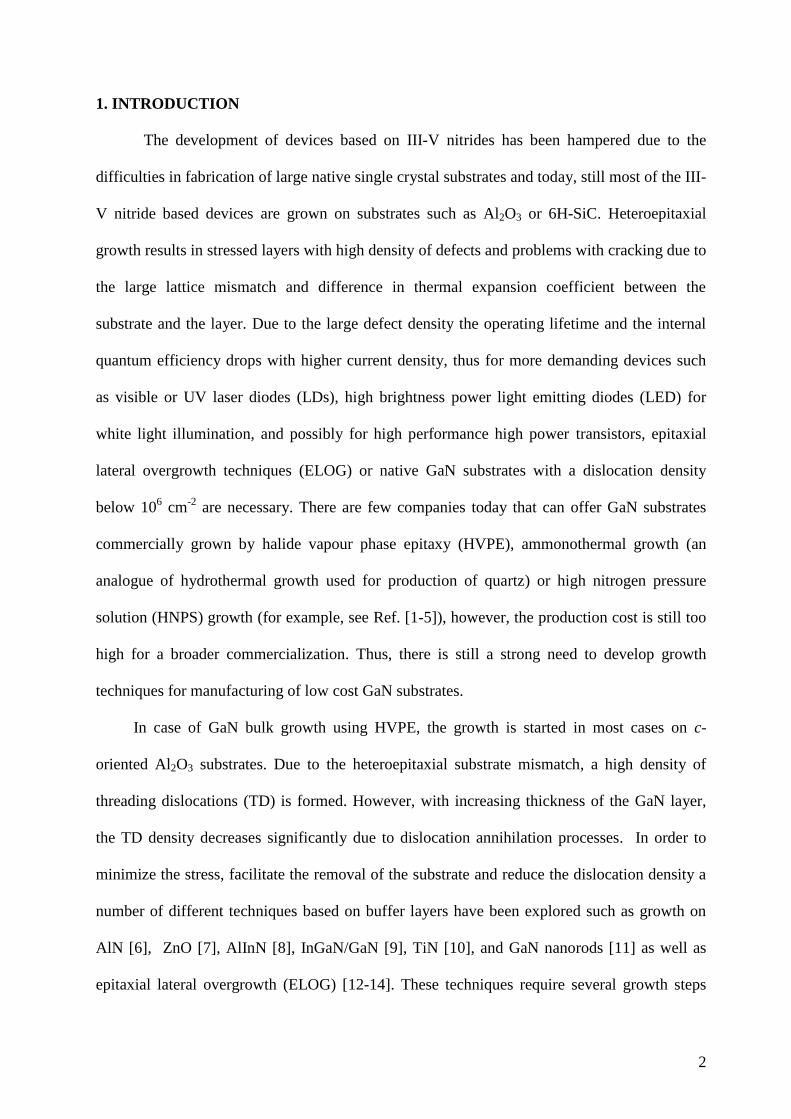
Figure 1 illustrates the different growth steps. Before growth of the LT-GaN buffer layer,
the sapphire substrate was exposed to NH3 during 10 min at 1050 oC. Thereafter, the
temperature was lowered to 600 oC and the LT-GaN buffer was grown. The V/III ratio at the
substrate was varied in the range 6-70 with a constant GaCl partial pressure of 2.8 mbar.
Within this range of V/III ratio the thickness of the buffer layers were varied in the range of 30
- 370 nm. N2 was used as a carrier gas in this step. After the deposition of the buffer layer, the
temperature was increased in presence of NH3 to 1050 o
C and the layer was annealed for 10
min in order to improve the crystallinity of the layers. Finally, the temperature was lowered to
1000oC where the thick high temperature GaN (HT-GaN) layer was grown. The growth was
done with a GaCl partial pressure at the substrate of ~20 mbar and a V/III ratio of 4. As carrier
gas, a mixture of H2 and N2 was used. With these process parameters, the typical growth rate
was ~200 µm/hr. The thickness of the HT-GaN was varied in the range between 20 µm and 2
mm.
The SEM and CL images were done with a Leo 1500 Gemini scanning electron
microscope equipped with a MonoCL system from Oxford Instruments using a 1200 lines/mm

5
grating blazed at 500 nm and detected by a Peltier-cooled photomultiplier. Structural
characterization was carried out with a Philips MRD XRD system with K1 (=1.54Å)
radiation source operating at 45 kV and 40 mA. A 11 mm2 point source and a parallel plate
collimator were used to analyze the diffracted radiation. The AFM measurements were
performed with a Veeco Dimension 3100 SPM system in tapping mode. The thickness of the
LT-GaN buffer layers were determined by white light reflectance spectroscopy (WLRS)
measurements. For very thin layers (<80 nm) when this technique cannot be used, the thickness
was estimated from the growth time.
3. RESULTS AND DISCUSSION
Figure 2 shows SEM images of the morphology as a function of LT-buffer layer thickness
grown with a V/III ratio of 37, before annealing [Fig.2 (a-d)], after annealing at 1050 oC for 10
min [Fig.2 (e-h)] and optical microscopy images after the buffer layers have been overgrown
with a 20 µm thick HT-GaN layer [Fig.2 (i-l)] .
For LT-buffer layers before annealing with a thickness of 100 nm or more [Fig.2 (b)-(d)],
we observe a continuous film consisting of GaN nanocrystallites with some inclusions of larger
crystallites. With increasing thickness, the size of the crystallites is decreasing. For the thinnest
film [Fig.2 (a)], large crystallites are dominating the surface and a continuous layer of GaN has
not been formed.
The subsequent annealing step [Fig.2 (e)-(h)] recrystallizes the layer and in case of LT-
buffers with a thickness of 100 nm or thicker, a continuous film consisting of hillocks with
some pits has been formed. We have also observed that with increasing thickness larger pits
and hillocks appear. For the thinnest buffer (Fig. 2(e)), some of the isolated crystallites become
larger at the expenses of the smaller ones due to Ostwald ripening.

6
Figure. 2 (i-l) shows the result when we grow a 20 µm thick HT-GaN film on the annealed
LT-GaN buffer layer. For the thinnest one (Fig. 2(i)), the morphology of the overgrown GaN
layer becomes poor since the substrate is only partially covered with LT-GaN. By using thicker
and fully coalesced buffer layers, we can grow single crystalline material (Fig. 2(j)-(l)).
However, we do observe a degradation of the morphology with increasing LT-buffer thickness
which we attribute to the increase of the pit size with increasing thickness of the LT-buffer
layer after annealing. Thus, the optimal morphology of the overgrown GaN layer is achieved
using a LT- GaN buffer layer with a thickness about 100-300 nm.
The influence of V/III-ratio on the morphology for LT buffer layers with a thickness of
~100 nm is illustrated before and after annealing at 1050oC for 10 min in Fig. 3 (a-d) and (e-h),
respectively. After annealing, these LT-buffers were overgrown with a 20 µm thick HT-GaN
layer and the morphology was studied by optical microscopy as shown in Fig.3 (i-l). All
studied LT-GaN films with an optimal thickness of ~100 nm were uniform for all studied V/III
ratios (Fig.3 (a-d)). However, with reduction of the V/III-ratio, the density of larger GaN
crystallites increases. After annealing at 1050oC (Fig. 3(e-h)), a rather dramatic change of the
morphology was observed. For high V/III ratio, a surface mainly consisted of hillocks was
observed, while for the lower V/III ratio the surface appeared to have crater-like features. The
morphology of the LT-GaN film after annealing has a strong influence on the quality of the
HT-GaN, as can be seen in Fig. 3(i-l). Thus, in order to obtain a smooth surface with a low pit
density, the growth should be performed on buffer layers synthesized in a nitrogen rich
environment, i.e. with a V/III ratio exceeding 17. However, in these films cracking formation
has been observed. This is a common problem of heteroepitaxy of GaN on Al2O3, when tensile
stress is generated by an island coalescence mechanism in the beginning of the growth on
substrates with large lattice mismatch [27, 28]. For HT-GaN layers grown on non-optimized

7
LT buffers, i.e. obtained with too low V/III ratio or which are too thin or too thick, no cracking
due to tensile stress was detected.
In order to find out how the surface roughness of the buffer layer influences the HT-GaN
quality, AFM measurements where done. The roughness of 100 nm thick LT-GaN buffer
layers before annealing is shown as a function of V/III ratio in Fig. 4(a). Fig. 4(b) shows how
the surface roughness develops with the LT-buffer thickness grown with a fixed V/III ratio of
37. As can be seen in Fig. 4(a) the roughness of the buffer layer increases step-like for samples
grown with a V/III ratio less than 37. The surface also became rougher with increasing LT
buffer thickness, although the tendency is less. The step-like increase in roughness for low
V/III ratios correlates with the drastic change from a hillock-like to a crater-like morphology
for LT buffers after annealing as was shown in Fig. 3 (e-h). The rougher surface of LT buffers
grown with low V/III ratios might prevent an efficient diffusion of species, lowering the
surface mobility during annealing, and hence, prevent formation of hillocks.
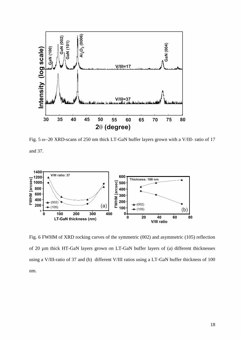
To determine crystallographic properties of the GaN buffer layers, XRD 2 scans were
done. Figure 5 shows the results for two LT-GaN layers with a thickness of ~250 nm grown
with a V/III-ratio of 17 and 37, respectively. The position of the peaks corresponds to wurtzite
GaN confirming that the LT-GaN buffer is wurtzite. Samples grown with a V/III ratio of 17
show except the main (001) peak additional features related to (100) and (101) reflections
indicating formation of misoriented domains. However, for LT-buffers obtained with a V/III-
ratio of 37 only peaks related to the c-planes (001) are observed.
Fig. 6 shows the results of XRD measurements for 20 µm thick HT-GaN layers grown on
different LT-GaN buffer layers. Fig. 6 (a) shows full width half maxima (FWHM) of XRD
rocking curves of the symmetric (002) and asymmetric (105) reflections versus thickness of the
LT-GaN buffer layers grown with a fixed V/III-ratio of 37. FWHM of the rocking curve for
both the asymmetric and symmetric reflections shows a non-monotonic behavior with a

8
minimum in the range of ~100-300 nm. Thus, according to these measurements, an optimal
buffer thickness is confirmed to be in the range of ~100-300 nm. The FWHM for a 20 µm thick
HT-GaN grown on such LT-buffers was about 400 and 250 arcsec for the symmetric (002) and
for the asymmetric (105) reflections, respectively. The increasing FWHM in case of the
thinnest LT-buffer layer is probably associated with the poor film coverage as shown in Fig.
2(a) while for the thicker buffers the broadening of the XRD peaks is likely related to increased
pit density in LT-buffers as was illustrated in Fig. 2(h).
We have also studied the XRD FWHM for the HT-GaN samples with a thickness of 20
µm grown on LT-GaN buffers obtained at different V/III ratio. With increasing V/III ratio, the
FWHM of the asymmetric (105) reflection dropped while the FWHM of the symmetric (002)
reflection is slightly increased as shown in Fig. 6(b).
The rocking curve FWHM has been associated with the TD density as the dislocations
distort particular reflection planes. The symmetric reflection such as the (002) reflection is
insensitive to pure edge type TD while scans related to the asymmetric planes like (105) are
progressively more sensitive to the edge-type TD [29]. Using this interpretation, our results
indicate that with increasing V/III-ratio, there is a decrease in the density of TD with an edge
component, but no significant change in the density of TD with screw components. It has been
shown in Ref. [30] that edge type threading dislocations are localized at grain boundaries.
Thus, a reduction in the density of edge type TD indicates larger diameter of the grains in the
film and, consequently, the grain diameter is increased in the HT-GaN films grown on LT-
buffer layers fabricated with higher V/III ratios.
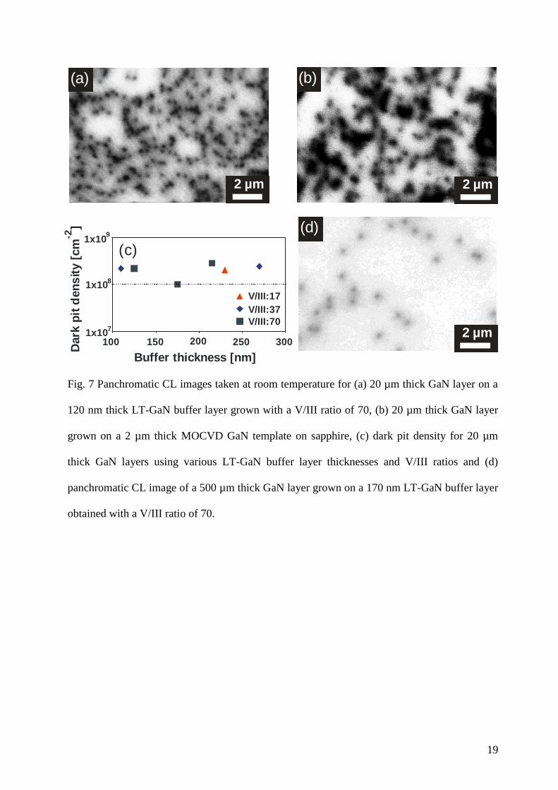
To further investigate the nature of the TD, additional characterization by CL was
performed. Fig. 7 (a) shows a panchromatic CL image of a 20 µm thick HT-GaN layers grown
on a 120 nm thick LT buffer layer, which was produced using a V/III ratio of 70. For
comparison we show in Fig. 7(b) a CL image of a 20 µm thick HT-GaN layer grown on a 2 µm
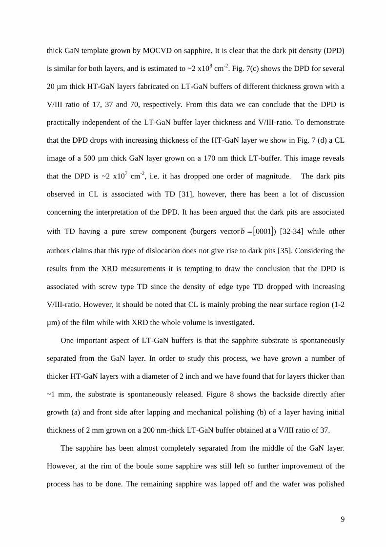
9
thick GaN template grown by MOCVD on sapphire. It is clear that the dark pit density (DPD)
is similar for both layers, and is estimated to ~2 x108 cm
-2. Fig. 7(c) shows the DPD for several
20 µm thick HT-GaN layers fabricated on LT-GaN buffers of different thickness grown with a
V/III ratio of 17, 37 and 70, respectively. From this data we can conclude that the DPD is
practically independent of the LT-GaN buffer layer thickness and V/III-ratio. To demonstrate
that the DPD drops with increasing thickness of the HT-GaN layer we show in Fig. 7 (d) a CL
image of a 500 µm thick GaN layer grown on a 170 nm thick LT-buffer. This image reveals
that the DPD is ~2 x107 cm
-2, i.e. it has dropped one order of magnitude. The dark pits
observed in CL is associated with TD [31], however, there has been a lot of discussion
concerning the interpretation of the DPD. It has been argued that the dark pits are associated
with TD having a pure screw component (burgers vector 0001b ) [32-34] while other
authors claims that this type of dislocation does not give rise to dark pits [35]. Considering the
results from the XRD measurements it is tempting to draw the conclusion that the DPD is
associated with screw type TD since the density of edge type TD dropped with increasing
V/III-ratio. However, it should be noted that CL is mainly probing the near surface region (1-2
µm) of the film while with XRD the whole volume is investigated.
One important aspect of LT-GaN buffers is that the sapphire substrate is spontaneously
separated from the GaN layer. In order to study this process, we have grown a number of
thicker HT-GaN layers with a diameter of 2 inch and we have found that for layers thicker than
~1 mm, the substrate is spontaneously released. Figure 8 shows the backside directly after
growth (a) and front side after lapping and mechanical polishing (b) of a layer having initial
thickness of 2 mm grown on a 200 nm-thick LT-GaN buffer obtained at a V/III ratio of 37.
The sapphire has been almost completely separated from the middle of the GaN layer.
However, at the rim of the boule some sapphire was still left so further improvement of the
process has to be done. The remaining sapphire was lapped off and the wafer was polished

10
from both sides. After polishing, it was revealed that the crystal had some cracks though they
have not penetrated the whole wafer so it still remains a diameter of 2 inch. The origin of the
cracks is unknown but there are several likely reasons such as cracking during cooling after the
growth and/or due to a non-optimized polishing process.
4. SUMMARY
We have studied growth of HT-GaN on LT-GaN buffers using different V/III ratios and
buffer growth times. The HT-GaN layers grown on LT-GaN buffers obtained with a V/III ratio
of 35 or 70 and a thickness of 100-300 nm demonstrate the smoothest surface morphology and
structural quality. The DPD of ~2108 cm
-2 measured on 20 µm thick HT-GaN layers were
found to be similar to DPD in HT-GaN layers grown on 2 µm-thick MOCVD fabricated GaN
templates. For a 500 µm-thick HT-GaN layer, DPD has dropped about one order of magnitude.
By using an optimized LT-GaN buffer layer, thick free freestanding 2’’ GaN substrates were
manufactured by spontaneous partial self-separation.

11
ACKNOWLEDGMENTS
This work was supported by the Swedish Research Science Council and the Swedish
Energy Agency.
12
REFERENCES
[1] Kyma Technologies www.kymatech.com, (2012, Aug. 21).
[2] Lumilog, France www.lumilog.com, (2012, Aug. 21).
[3] TopGan Ltd, www.topgan.fr.pl, (2012, Aug. 21).
[4] Ammono S.A., ammono.com, (2012, Dec. 11).
[5] T. Hashimoto, F. Wu, J.S. Speck, S. Nakamura, Nature Materials, 6 (8), (2007), 568
[6] E. Valcheva, T. Paskova, S. Tungasmita, P.O.A. Persson, J. Birch, E.B. Svedberg, L.
Hultman and B. Monemar, Appl. Phys. Lett., 76 (2000), 1860
[7] T. Detchprohm, K. Hiramatsu, H. Amano and I. Akasaki. Appl. Phys. Lett., 61 (1992),
2688.
[8] C. Hemmingsson, M. Boota, R. O. Rahmatalla, M. Junaid, G. Pozina, J. Birch, and B.
Monemar, J. Cryst. Growth, 311 (2009), 292
[9] D. Gogova, D. Siche, A. Kwasniewski, M. Schmidbauer, R. Fornari, C. Hemmingsson,
R. Yakimova and B. Monemar, Phys. Status Solidi C, 7 (2010), 1756
[10] Y. Oshima, T. Eri, M. Shibata, H. Sunakawa and A. Usui, Phys. Status Solidi A,
194 (2002), 554
[11] C. L. Chao, C. H. Chiu, Y. J. Lee, H. C. Kuo, P.-C. Liu, J. D. Tsay, and S. J. Cheng,
Appl. Phys. Lett., 95 (2009), 051905
[12] A. Usui, H. Sunakawa, A. Sakai, and A.A. Yamaguchi, Jpn. J. Appl. Phys., 36 (1997),
L899
[13] G. Nataf, B. Beaumont, A. Bouillé, S. Haffouz, M. Vaille, and P. Gibart J. Cryst.
Growth, 192 (1998), 73
[14] F. Lipski, T. Wunderer, S. Schwaiger and F. Scholz, Phys. Status Solidi A, 207
(2010), 128

13
[15] I. Akasaki, H. Amano, Y. Koide, K. Hiramatsu and N. Sawaki, J. Cryst. Growth, 98
(1989), 209
[16] M. Sumiya, N. Ogusu, Y. Yotsuda, M. Itoh, S. Fuke, T. Nakamura, S. Mochizuki, T.
Sano, S. Kamiyama, H. Amano, and I. Akasaki, J. Appl. Phys., 93 (2003), 1311
[17] P.R. Tavernier, E.V. Etzkorn, Y. Wang and D.R. Clarke, Appl. Phys. Lett., 77 (2000),
1804
[18] H. M. Kim, J. E. Oh and T. W. Kang , H. M. Kim, J. E. Oh and T. W. Kang, Mater.
Lett., 47 (2001), 276
[19] K. Motoki, T. Okahisa, S. Nakahata, N. Matsumoto, H. Kimura, H. Kasai, K.
Takemoto, K. Uematsu, M. Ueno, Y. Kumagai, A. Koukitu and H. Seki, Mater. Sci. Eng.,
B 93 (2002), 123
[20] M.K. Kelly, R.P. Vaudo, V.M. Phanse, L. Gorgens, O. Ambacher and M. Stutzmann,
Jpn. J. Appl. Phys., 38 (1999), L217
[21] D. Gogova, A. Kasic, H. Larsson, C. Hemmingsson, B. Monemar, F. Toumisto, K
Saarinen, L. Dobos, B. Pécs, P. Gibart and B. Beaumont, J. Appl. Phys., 96 (2004), 799
[22] P. Gibart, B. Beaumont, and P. Vennegues, in “Nitride Semiconductors, Handbook on
Materials and Devices, Eds P Ruterana, M Albrecht and J Neugebauer, Wiley-VCH (2003),
45.
[23] Y. Oshima, T. Eri, M. Shibata, H. Sunakawa, K. Kobayashi, T. Ichihashi, and A. Usui,
Jpn. J. Appl. Phys., 42 (2003), L1
[24] M. Sumiya, N. Ogusu, Y. Yotsuda, M. Itoh, S. Fuke, T. Nakamura, S. Mochizuki, T.
Sano, S. Kamiyama, H. Amano, and I. Akasaki, J. Appl. Phys., 93 (2003), 1311
[25] C. Hemmingsson, P.P. Paskov, G. Pozina, M. Heuken, B. Schineller and B. Monemar,
Superlattices Microstruct., 40 (2006), 205
[26] C. Hemmingsson, G. Pozina, M. Heuken, B. Schineller and B. Monemar

14
J. Crystal Growth , 310 (2008), 906
[27] E.V. Etzkorn and D.R. Clarke, J. Appl. Phys., 89 (2001), 1025
[28] W.D. Nix and B.M. Clemens, J. Mater. Res., 14 (1999), 3467
[29] B. Heying, X.H Wu,, S. Keller, Y. Li, D. Kapolnek, B.P. Keller, S.P. Denbaars and
J.S. Speck, Appl. Phys. Lett., 68 (1996), 643
[30] R. Chierchia, T. Böttcher, H. Heinke, S. Einfeldt, S. Figge and D. Hommel, J. Appl.
Phys., 93 (2003), 8918
[31] S.J. Rosner, E.C. Carr, M. J. Ludowise, G. Girolami, and H.I. Erikson, Appl. Phys.
Lett., 70 ( 1997), 420
[32] E.G. Braze, M.A. Chin and V. Narayanamurti, Appl. Phys. Lett., 74 (1999), 2367
[33] G. Koley and M.G. Spencer, Appl. Phys. Lett., 78 (2001), 2873
[34] T. Hino, S. Tomiya, T. Miyajima, K. Yanashima, S. Hashimoto and M. Ikeda, Appl.
Phys. Lett., 76 (2000), 3421
[35] M. Albrecht, J.L. Weyher, B. Lucznik, I. Grzegory and S. Porowski, Appl. Phys. Lett.,
92 (2008), 231909
15
Figure captions
Fig. 1 Schematic diagram of the growth process.

16
Fig. 2 SEM images of the morphology as a function of buffer layer thickness for LT-GaN
layers grown with a V/III ratio of 37, before annealing (a-d), after annealing at 1050 oC for 10
min (e-h) and microscopy images after they have been overgrown with a 20 µm thick HT-GaN
layer (i-l) .

17
Fig. 3 SEM images of the morphology as a function of V/III-ratio for LT buffer layers with a
thickness of ~100nm, before annealing (a-d), after annealing at 1050 oC for 10 min (e-h) and
microscopy images after they have been overgrown with a 20 µm thick HT-GaN layer (i-l).
Fig. 4 (a) Roughness (RMS) for a 100 nm thick LT-GaN before annealing using various V/III
ratios and (b) roughness of LT-GaN buffers before annealing versus thicknesses using a V/III
ratio of 37. The line is guidance for the eye.
18
Fig. 5 2 XRD-scans of 250 nm thick LT-GaN buffer layers grown with a V/III- ratio of 17
and 37.
Fig. 6 FWHM of XRD rocking curves of the symmetric (002) and asymmetric (105) reflection
of 20 µm thick HT-GaN layers grown on LT-GaN buffer layers of (a) different thicknesses
using a V/III-ratio of 37 and (b) different V/III ratios using a LT-GaN buffer thickness of 100
nm.
19
Fig. 7 Panchromatic CL images taken at room temperature for (a) 20 µm thick GaN layer on a
120 nm thick LT-GaN buffer layer grown with a V/III ratio of 70, (b) 20 µm thick GaN layer
grown on a 2 µm thick MOCVD GaN template on sapphire, (c) dark pit density for 20 µm
thick GaN layers using various LT-GaN buffer layer thicknesses and V/III ratios and (d)
panchromatic CL image of a 500 µm thick GaN layer grown on a 170 nm LT-GaN buffer layer
obtained with a V/III ratio of 70.
1x10⁷
100 150 200 250
Dark
pit
den
sit
y [
cm
]-2
Buffer thickness [nm]
V/III:17
V/III:37
V/III:70
1x10⁸
1x10⁹
300
(c)
2 µm
(d)
2 µm
(b)
2 µm
(a)

20
Fig. 8 Images of a 2 mm thick GaN layer grown on a LT-buffer layer (thickness=200nm, V/III-
ratio=37). (a) backside (nitrogen side) with some remaining sapphire and (b) front side
(gallium side) after removal of sapphire and polishing.