NPIC6C595 Power logic 8-bit shift register; open-drain outputs · NPIC6C595 All information...
20
1. General description The NPIC6C595 is an 8-bit serial-in/serial or parallel-out shift register with a storage register and open-drain outputs. Both the shift and storage register have separate clocks. The device features a serial input (DS) and a serial output (Q7S) to enable cascading and an asynchronous reset input (MR ). A LOW on MR resets both the shift register and storage register. Data is shifted on the LOW-to-HIGH transitions of the SHCP input. The data in the shift register is transferred to the storage register on a LOW-to-HIGH transition of the STCP input and to the Q7S output on a LOW-to-HIGH transition of the SHCP input. If both clocks are connected together, the shift register is always one clock pulse ahead of the storage register. Data in the storage register drives the gate of the output extended-drain NMOS transistor whenever the output enable input (OE ) is LOW. A HIGH on OE causes the outputs to assume a high-impedance OFF-state. Operation of the OE input does not affect the state of the registers. The open-drain outputs are 33 V/100 mA continuous current extended-drain NMOS transistors designed for use in systems that require moderate load power such as LEDs. Integrated voltage clamps in the outputs provide protection against inductive transients. This feature makes the device suitable for power driver applications such as relay, solenoids and other low-current or medium-voltage loads. 2. Features and benefits Specified from 40 C to +125 C Low R DSon Eight Power EDNMOS transistor outputs of 100 mA continuous current 250 mA current limit capability Output clamping voltage 33 V 30 mJ avalanche energy capability All registers cleared with single input Low power consumption ESD protection: HBM JDS-001 Class 2 exceeds 2500 V CDM JESD22-C101E exceeds 1000 V 3. Applications LED sign Graphic status panel Fault status indicator NPIC6C595 Power logic 8-bit shift register; open-drain outputs Rev. 1 — 20 August 2012 Product data sheet
Transcript of NPIC6C595 Power logic 8-bit shift register; open-drain outputs · NPIC6C595 All information...
1. General description
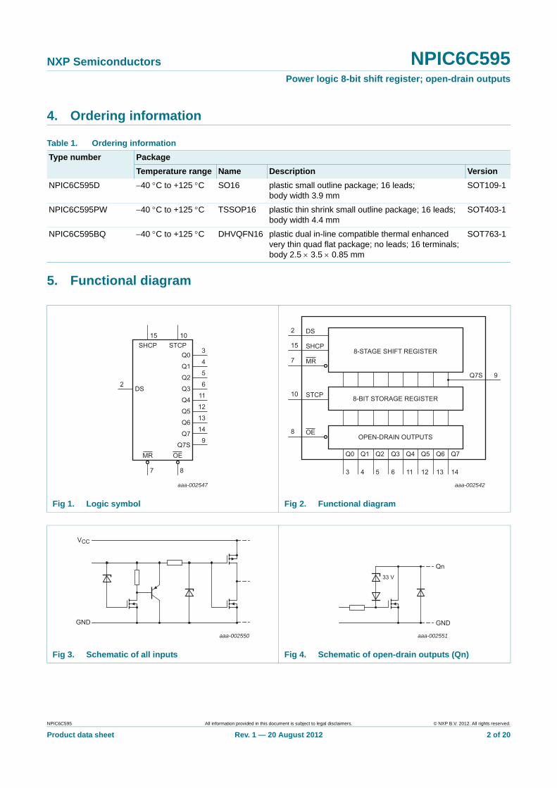
The NPIC6C595 is an 8-bit serial-in/serial or parallel-out shift register with a storage register and open-drain outputs. Both the shift and storage register have separate clocks. The device features a serial input (DS) and a serial output (Q7S) to enable cascading and an asynchronous reset input (MR). A LOW on MR resets both the shift register and storage register. Data is shifted on the LOW-to-HIGH transitions of the SHCP input. The data in the shift register is transferred to the storage register on a LOW-to-HIGH transition of the STCP input and to the Q7S output on a LOW-to-HIGH transition of the SHCP input. If both clocks are connected together, the shift register is always one clock pulse ahead of the storage register. Data in the storage register drives the gate of the output extended-drain NMOS transistor whenever the output enable input (OE) is LOW. A HIGH on OE causes the outputs to assume a high-impedance OFF-state. Operation of the OE input does not affect the state of the registers. The open-drain outputs are 33 V/100 mA continuous current extended-drain NMOS transistors designed for use in systems that require moderate load power such as LEDs. Integrated voltage clamps in the outputs provide protection against inductive transients. This feature makes the device suitable for power driver applications such as relay, solenoids and other low-current or medium-voltage loads.
2. Features and benefits
Specified from 40 C to +125 C Low RDSon
Eight Power EDNMOS transistor outputs of 100 mA continuous current
250 mA current limit capability
Output clamping voltage 33 V
30 mJ avalanche energy capability
All registers cleared with single input
Low power consumption
ESD protection:
HBM JDS-001 Class 2 exceeds 2500 V
CDM JESD22-C101E exceeds 1000 V
3. Applications
LED sign
Graphic status panel
Fault status indicator
NPIC6C595Power logic 8-bit shift register; open-drain outputsRev. 1 — 20 August 2012 Product data sheet
NXP Semiconductors NPIC6C595Power logic 8-bit shift register; open-drain outputs
4. Ordering information
5. Functional diagram
Table 1. Ordering information
Type number Package
Temperature range Name Description Version
NPIC6C595D 40 C to +125 C SO16 plastic small outline package; 16 leads; body width 3.9 mm
SOT109-1
NPIC6C595PW 40 C to +125 C TSSOP16 plastic thin shrink small outline package; 16 leads; body width 4.4 mm
SOT403-1
NPIC6C595BQ 40 C to +125 C DHVQFN16 plastic dual in-line compatible thermal enhanced very thin quad flat package; no leads; 16 terminals; body 2.5 3.5 0.85 mm
SOT763-1
Fig 1. Logic symbol Fig 2. Functional diagram
Q0
DS
SHCP
MR
STCP
Q1
3
15 10
2
4
5
6
11
12
13
14
9
7 8
Q2
Q3
Q4
Q5
Q6
Q7
Q7SOE
aaa-002547
3
Q0
4
Q1
5
Q2
6
Q3
OPEN-DRAIN OUTPUTS
8-BIT STORAGE REGISTER
8-STAGE SHIFT REGISTER
11
Q4
12
Q5
13
Q6
14
Q7
OE
STCP
MR
SHCP
Q7S
DS2
15
9
7
10
8
aaa-002542
Fig 3. Schematic of all inputs Fig 4. Schematic of open-drain outputs (Qn)
aaa-002550
GND
VCC
aaa-002551
GND
Qn33 V
NPIC6C595 All information provided in this document is subject to legal disclaimers. © NXP B.V. 2012. All rights reserved.
Product data sheet Rev. 1 — 20 August 2012 2 of 20

NXP Semiconductors NPIC6C595Power logic 8-bit shift register; open-drain outputs
Fig 5. Logic diagram
aaa-002543
GND
QD D Q
Q7S
Q7
STAGE 7STAGE 1 TO 6STAGE 0
0CP
D QR
R
CP
D QDS
SHCP
MR
STCP
OE
CPR
LATCH7
LATCH
LATCH
D QR
CP
LATCH
Q6Q5Q4Q3Q2Q1Q0
GND
Fig 6. Timing diagram
aaa-002553
7 6 5 4 3 2 15 VGND
SHCP
OE
DS
5 VGND
5 VGND
5 VGND
5 VGND
VOHVOL
0
STCP
MR
Q1
NPIC6C595 All information provided in this document is subject to legal disclaimers. © NXP B.V. 2012. All rights reserved.
Product data sheet Rev. 1 — 20 August 2012 3 of 20
NXP Semiconductors NPIC6C595Power logic 8-bit shift register; open-drain outputs
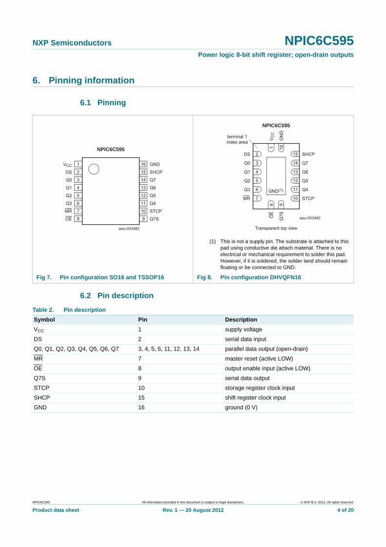
6. Pinning information
6.1 Pinning
6.2 Pin description
(1) This is not a supply pin. The substrate is attached to this pad using conductive die attach material. There is no electrical or mechanical requirement to solder this pad. However, if it is soldered, the solder land should remain floating or be connected to GND.
Fig 7. Pin configuration SO16 and TSSOP16 Fig 8. Pin configuration DHVQFN16
NPIC6C595
VCC GND
DS SHCP
Q0 Q7
Q1 Q6
Q2 Q5
Q3 Q4
MR STCP
OE Q7S
aaa-003482
1
2
3
4
5
6
7
8
10
9
12
11
14
13
16
15
aaa-003483
NPIC6C595
MR STCP
Q3 Q4
Q2
GND(1)
Q5
Q1 Q6
Q0 Q7
DS SHCP
OE
Q7S
VC
C
GN
D
Transparent top view
7 10
6 11
5 12
4 13
3 14
2 15
8 9
1 16
terminal 1index area
Table 2. Pin description
Symbol Pin Description
VCC 1 supply voltage
DS 2 serial data input
Q0, Q1, Q2, Q3, Q4, Q5, Q6, Q7 3, 4, 5, 6, 11, 12, 13, 14 parallel data output (open-drain)
MR 7 master reset (active LOW)
OE 8 output enable input (active LOW)
Q7S 9 serial data output
STCP 10 storage register clock input
SHCP 15 shift register clock input
GND 16 ground (0 V)
NPIC6C595 All information provided in this document is subject to legal disclaimers. © NXP B.V. 2012. All rights reserved.
Product data sheet Rev. 1 — 20 August 2012 4 of 20
NXP Semiconductors NPIC6C595Power logic 8-bit shift register; open-drain outputs
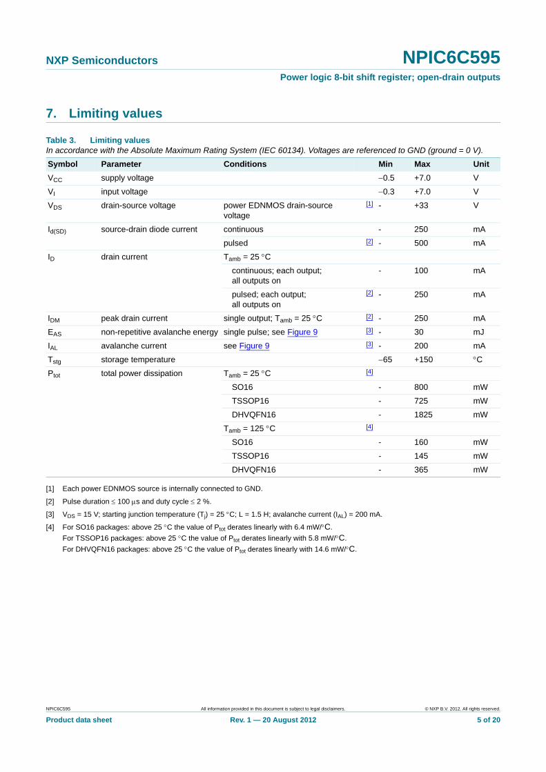
7. Limiting values
[1] Each power EDNMOS source is internally connected to GND.
[2] Pulse duration 100 s and duty cycle 2 %.
[3] VDS = 15 V; starting junction temperature (Tj) = 25 C; L = 1.5 H; avalanche current (IAL) = 200 mA.
[4] For SO16 packages: above 25 C the value of Ptot derates linearly with 6.4 mW/C.
For TSSOP16 packages: above 25 C the value of Ptot derates linearly with 5.8 mW/C.
For DHVQFN16 packages: above 25 C the value of Ptot derates linearly with 14.6 mW/C.
Table 3. Limiting valuesIn accordance with the Absolute Maximum Rating System (IEC 60134). Voltages are referenced to GND (ground = 0 V).
Symbol Parameter Conditions Min Max Unit
VCC supply voltage 0.5 +7.0 V
VI input voltage 0.3 +7.0 V
VDS drain-source voltage power EDNMOS drain-source voltage
[1] - +33 V
Id(SD) source-drain diode current continuous - 250 mA
pulsed [2] - 500 mA
ID drain current Tamb = 25 C
continuous; each output; all outputs on
- 100 mA
pulsed; each output; all outputs on
[2] - 250 mA
IDM peak drain current single output; Tamb = 25 C [2] - 250 mA
EAS non-repetitive avalanche energy single pulse; see Figure 9 [3] - 30 mJ
IAL avalanche current see Figure 9 [3] - 200 mA
Tstg storage temperature 65 +150 C
Ptot total power dissipation Tamb = 25 C [4]
SO16 - 800 mW
TSSOP16 - 725 mW
DHVQFN16 - 1825 mW
Tamb = 125 C [4]
SO16 - 160 mW
TSSOP16 - 145 mW
DHVQFN16 - 365 mW
NPIC6C595 All information provided in this document is subject to legal disclaimers. © NXP B.V. 2012. All rights reserved.
Product data sheet Rev. 1 — 20 August 2012 5 of 20

NXP Semiconductors NPIC6C595Power logic 8-bit shift register; open-drain outputs
7.1 Test circuit and waveform
8. Recommended operating conditions
[1] Pulse duration 100 s and duty cycle 2 %.
[2] This technique should limit Tj Tamb to 10 C maximum.
9. Static characteristics
(1) The word generator has the following characteristics: tr, tf 10 ns; ZO = 50 .
(2) The input pulse duration (tW) is increased until peak current IAL = 200 mA. Energy test level is defined as: EAS = IAL V(BR)DSS tAL/2 = 30 mJ.
Fig 9. Test circuit and waveform for measuring single-pulse avalanche energy
aaa-002556
WORDGENERATOR(1)
DUT
7 1
5 V
15 V
5 V
min
0 VlAL = 200 mA
V(BR)DSS = 33 V
ID
VDS
30 Ω
1.5 mH
16GNDOE
STCP
DS
SHCP
MR
VCC
VDS
lD
Qn
15
2
10
3-6,11-14
8
tw(2) tAL
Table 4. Recommended operating conditions
Symbol Parameter Conditions Min Typ Max Unit
VCC supply voltage 4.5 - 5.5 V
VI input voltage 0 - 5.5 V
ID drain current pulsed drain output current; VCC = 5 V; Tamb = 25 C; all outputs on
[1][2] - - 250 mA
Tamb ambient temperature 40 - +125 C
Table 5. Static characteristicsAt recommended operating conditions. Voltages are referenced to GND (ground = 0 V).
Symbol Parameter Conditions VCC = 5.0 V; Tamb = 25 C Unit
Min Typ Max
VIH HIGH-level input voltage
VCC = 4.5 V to 5.5 V 0.85VCC - - V
VIL LOW-level input voltage
VCC = 4.5 V to 5.5 V - - 0.15VCC V
VOH HIGH-level output voltage
serial data output Q7S; VI = VIH or VIL
IO = 20 A; VCC = 4.5 V 4.4 4.49 - V
IO = 4 mA; VCC = 4.5 V 4.0 4.2 - V
NPIC6C595 All information provided in this document is subject to legal disclaimers. © NXP B.V. 2012. All rights reserved.
Product data sheet Rev. 1 — 20 August 2012 6 of 20
NXP Semiconductors NPIC6C595Power logic 8-bit shift register; open-drain outputs
[1] This technique should limit Tj Tamb to 10 C maximum.
[2] These parameters are measured with voltage-sensing contacts separate from the current-carrying contacts.
[3] Nominal output current is defined for a consistent comparison between devices from different sources. It is the current that produces a
voltage drop of 0.5 V at Tamb = 85 C.
VOL LOW-level output voltage
serial data output Q7S; VI = VIH or VIL
IO = 20 A; VCC = 4.5 V - 0.005 0.1 V
IO = 4 mA; VCC = 4.5 V - 0.3 0.5 V
IIH HIGH-level input current
VCC = 5.5 V; VI = VCC - - 1 A
IIL LOW-level input current
VCC = 5.5 V; VI = 0 V - - 1 A
V(BR)DSS drain-source breakdown voltage
ID = 1 mA 33 37 - V
VSD source-drain voltage
diode forward voltage; IF = 100 mA - 0.85 1.2 V
ICC supply current logic supply current; VCC = 5.5 V; VI = VCC or GND
all outputs off - 0.004 200 A
all outputs on - 0.006 500 A
all outputs off; SHCP = 5 MHz; CL = 30 pF; see Figure 14 and Figure 16
- 0.75 5 mA
IO(nom) nominal output current
VDS = 0.5 V; Tamb = 85 C; Iout = ID [1][2][3] - 140 - mA
IDSX drain cut-off current
VCC = 5.5 V; VDS = 30 V - 0.002 0.2 A
VCC = 5.5 V; VDS = 30 V; Tamb = 125 C - 0.15 0.3 A
RDSon drain-source on-state resistance
see Figure 17 and Figure 18 [1][2]
VCC = 4.5 V; ID = 50 mA - 3.0 9
VCC = 4.5 V; ID = 50 mA; Tamb = 125 C 5.4 12
VCC = 4.5 V; ID = 100 mA - 3.1 10
Table 5. Static characteristics …continuedAt recommended operating conditions. Voltages are referenced to GND (ground = 0 V).
Symbol Parameter Conditions VCC = 5.0 V; Tamb = 25 C Unit
Min Typ Max
NPIC6C595 All information provided in this document is subject to legal disclaimers. © NXP B.V. 2012. All rights reserved.
Product data sheet Rev. 1 — 20 August 2012 7 of 20
NXP Semiconductors NPIC6C595Power logic 8-bit shift register; open-drain outputs
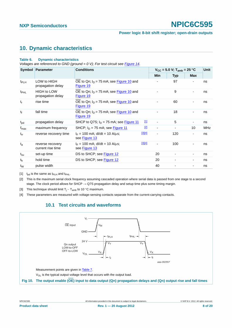
10. Dynamic characteristics
[1] tpd is the same as tPLH and tPHL.
[2] This is the maximum serial clock frequency assuming cascaded operation where serial data is passed from one stage to a second
stage. The clock period allows for SHCP → Q7S propagation delay and setup time plus some timing margin.
[3] This technique should limit Tj Tamb to 10 C maximum.
[4] These parameters are measured with voltage-sensing contacts separate from the current-carrying contacts.
10.1 Test circuits and waveforms
Table 6. Dynamic characteristicsVoltages are referenced to GND (ground = 0 V); For test circuit see Figure 14.
Symbol Parameter Conditions VCC = 5.0 V; Tamb = 25 C Unit
Min Typ Max
tPLH LOW to HIGH propagation delay
OE to Qn; ID = 75 mA; see Figure 10 and Figure 19
- 97 - ns
tPHL HIGH to LOW propagation delay
OE to Qn; ID = 75 mA; see Figure 10 and Figure 19
- 9 - ns
tr rise time OE to Qn; ID = 75 mA; see Figure 10 and Figure 19
- 60 - ns
tf fall time OE to Qn; ID = 75 mA; see Figure 10 and Figure 19
- 18 - ns
tpd propagation delay SHCP to Q7S; ID = 75 mA; see Figure 11 [1] - 5 - ns
fmax maximum frequency SHCP; ID = 75 mA; see Figure 11 [2] - - 10 MHz
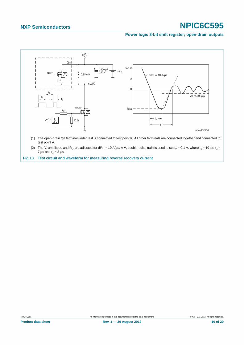
trr reverse recovery time IF = 100 mA; dI/dt = 10 A/s; see Figure 13
[3][4] - 120 - ns
ta reverse recovery current rise time
IF = 100 mA; dI/dt = 10 A/s; see Figure 13
[3][4] - 100 - ns
tsu set-up time DS to SHCP; see Figure 12 20 - - ns
th hold time DS to SHCP; see Figure 12 20 - - ns
tW pulse width 40 - - ns
Measurement points are given in Table 7.
VOL is the typical output voltage level that occurs with the output load.
Fig 10. The output enable (OE) input to data output (Qn) propagation delays and (Qn) output rise and fall times
GND
24 V
tPLH
tr
VM
VI
VOLVX VX
VY
tPHL
tf
VYQn outputLOW-to-OFFOFF-to-LOW
OE input
aaa-002557
NPIC6C595 All information provided in this document is subject to legal disclaimers. © NXP B.V. 2012. All rights reserved.
Product data sheet Rev. 1 — 20 August 2012 8 of 20
NXP Semiconductors NPIC6C595Power logic 8-bit shift register; open-drain outputs
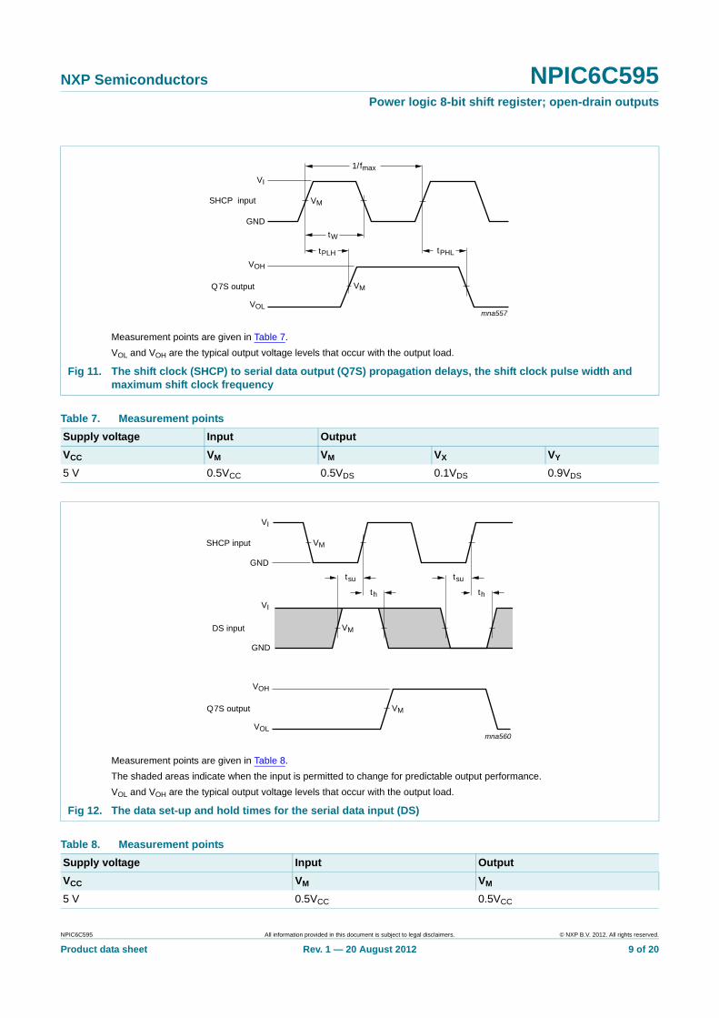
Measurement points are given in Table 7.
VOL and VOH are the typical output voltage levels that occur with the output load.
Fig 11. The shift clock (SHCP) to serial data output (Q7S) propagation delays, the shift clock pulse width and maximum shift clock frequency
mna557
SHCP input
Q7S output
tPLH tPHL
tW
1/fmax
VM
VOH
VI
GND
VOL
VM
Table 7. Measurement points
Supply voltage Input Output
VCC VM VM VX VY
5 V 0.5VCC 0.5VDS 0.1VDS 0.9VDS
Measurement points are given in Table 8.
The shaded areas indicate when the input is permitted to change for predictable output performance.
VOL and VOH are the typical output voltage levels that occur with the output load.
Fig 12. The data set-up and hold times for the serial data input (DS)
mna560
GND
GND
th
tsu
th
tsu
VM
VM
VM
VI
VOH
VOL
VI
Q7S output
SHCP input
DS input
Table 8. Measurement points
Supply voltage Input Output
VCC VM VM
5 V 0.5VCC 0.5VCC
NPIC6C595 All information provided in this document is subject to legal disclaimers. © NXP B.V. 2012. All rights reserved.
Product data sheet Rev. 1 — 20 August 2012 9 of 20
NXP Semiconductors NPIC6C595Power logic 8-bit shift register; open-drain outputs
(1) The open-drain Qn terminal under test is connected to test point K. All other terminals are connected together and connected to test point A.
(2) The VI amplitude and RG are adjusted for dI/dt = 10 A/s. A VI double-pulse train is used to set IF = 0.1 A, where t1 = 10 s, t2 = 7 s and t3 = 3 s.
Fig 13. Test circuit and waveform for measuring reverse recovery current
aaa-002560
IF
DUT
Qn
15 V
driverRG
G 50 Ω
2500 μF250 V
0.85 mH
K(1)
A(1)
t1
t2
t3
VI(2)
0.1 A
di/dt = 10 A/μsIF
ta
trr
0
25 % of lRM
IRM
NPIC6C595 All information provided in this document is subject to legal disclaimers. © NXP B.V. 2012. All rights reserved.
Product data sheet Rev. 1 — 20 August 2012 10 of 20
NXP Semiconductors NPIC6C595Power logic 8-bit shift register; open-drain outputs
(1) The word generator has the following characteristics: tr, tf 10 ns; tW = 300 ns; pulsed repetition rate (PRR) = 5 kHz; ZO = 50 .
(2) CL includes probe and jig capacitance.
Test data is given in Table 9. Definitions for test circuit:
VDS = External voltage for Power EDNMOS drain-source voltage.
RL = Load resistance.
CL = Load capacitance including jig and probe capacitance.
Fig 14. Test circuit for measuring switching times
7
15
2
10
16
GND
1
tW
tW
90 %VM
10 %0 V
positivepulse
negativepulse
VI
0 V
VI
VM
VM
VM
90 %
tf
tr
tr
tf
10 %
WORDGENERATOR (1)
8
VCC
5 V
Qn
3, 4, 5, 611, 12,13, 14
aaa-002561
VDS = 15 V
RL
CL (2)
MR
DS
OE
SHCP
STCP
Table 9. Test data
Supply voltage Input Load
VI tr, tf VM CL RL
5 V 5 V 10 ns 50 % 30 pF 200
NPIC6C595 All information provided in this document is subject to legal disclaimers. © NXP B.V. 2012. All rights reserved.
Product data sheet Rev. 1 — 20 August 2012 11 of 20
NXP Semiconductors NPIC6C595Power logic 8-bit shift register; open-drain outputs
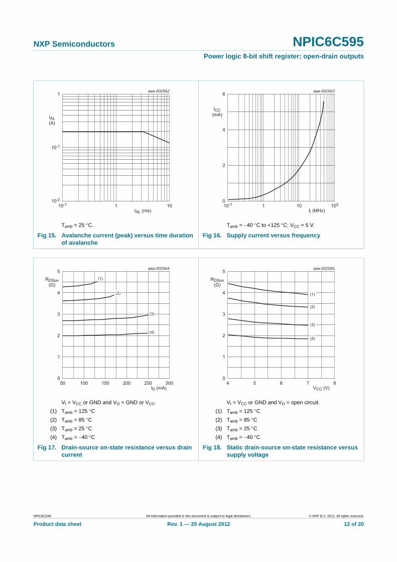
Tamb = 25 C. Tamb = 40 C to +125 C; VCC = 5 V.
Fig 15. Avalanche current (peak) versus time duration of avalanche
Fig 16. Supply current versus frequency
tAL (ms)10-1 101
aaa-002562
10-1
1
IAL(A)
10-2
aaa-002563
2
4
6
lCC(mA)
0
fi (MHz)10-1 102101
VI = VCC or GND and VO = GND or VCC.
(1) Tamb = 125 C
(2) Tamb = 85 C
(3) Tamb = 25 C
(4) Tamb = 40 C
VI = VCC or GND and VO = open circuit.
(1) Tamb = 125 C
(2) Tamb = 85 C
(3) Tamb = 25 C
(4) Tamb = 40 C
Fig 17. Drain-source on-state resistance versus drain current
Fig 18. Static drain-source on-state resistance versus supply voltage
lD (mA)50 300250150 200100
aaa-002564
2
3
1
4
5
RDSon(Ω)
0
(4)
(3)
(1)
(2)
VCC (V)4 875 6
aaa-002565
2
3
1
4
5
RDSon(Ω)
0
(1)
(2)
(3)
(4)
NPIC6C595 All information provided in this document is subject to legal disclaimers. © NXP B.V. 2012. All rights reserved.
Product data sheet Rev. 1 — 20 August 2012 12 of 20
NXP Semiconductors NPIC6C595Power logic 8-bit shift register; open-drain outputs
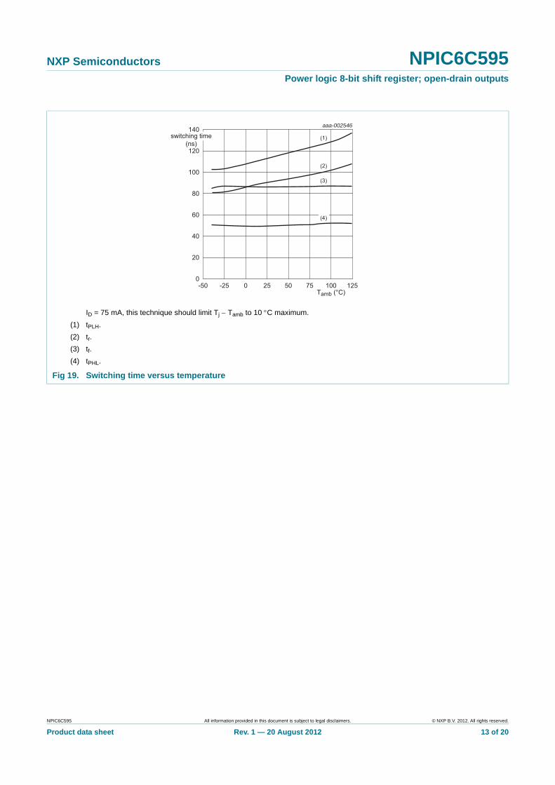
ID = 75 mA, this technique should limit Tj Tamb to 10 C maximum.
(1) tPLH.
(2) tr.
(3) tf.
(4) tPHL.
Fig 19. Switching time versus temperature
aaa-002546
Tamb (°C)-50 0 50 100 1257525-25
140switching time
(ns)
0
20
40
60
80
100
120
(1)
(2)
(3)
(4)
NPIC6C595 All information provided in this document is subject to legal disclaimers. © NXP B.V. 2012. All rights reserved.
Product data sheet Rev. 1 — 20 August 2012 13 of 20
NXP Semiconductors NPIC6C595Power logic 8-bit shift register; open-drain outputs
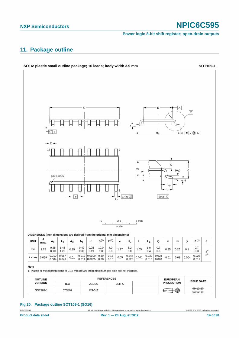
11. Package outline
Fig 20. Package outline SOT109-1 (SO16)
X
w M
θ
AA1
A2
bp
D
HE
Lp
Q
detail X
E
Z
e
c
L
v M A
(A )3
A
8
9
1
16
y
pin 1 index
UNITA
max. A1 A2 A3 bp c D(1) E(1) (1)e HE L Lp Q Zywv θ
REFERENCESOUTLINEVERSION
EUROPEANPROJECTION ISSUE DATE
IEC JEDEC JEITA
mm
inches
1.750.250.10
1.451.25
0.250.490.36
0.250.19
10.09.8
4.03.8
1.276.25.8
0.70.6
0.70.3 8
0
o
o
0.25 0.1
DIMENSIONS (inch dimensions are derived from the original mm dimensions)
Note
1. Plastic or metal protrusions of 0.15 mm (0.006 inch) maximum per side are not included.
1.00.4
SOT109-199-12-2703-02-19
076E07 MS-012
0.0690.0100.004
0.0570.049
0.010.0190.014
0.01000.0075
0.390.38
0.160.15
0.05
1.05
0.0410.2440.228
0.0280.020
0.0280.012
0.01
0.25
0.01 0.0040.0390.016
0 2.5 5 mm
scale
SO16: plastic small outline package; 16 leads; body width 3.9 mm SOT109-1
NPIC6C595 All information provided in this document is subject to legal disclaimers. © NXP B.V. 2012. All rights reserved.
Product data sheet Rev. 1 — 20 August 2012 14 of 20

NXP Semiconductors NPIC6C595Power logic 8-bit shift register; open-drain outputs
Fig 21. Package outline SOT403-1 (TSSOP16)
UNIT A1 A2 A3 bp c D (1) E (2) (1)e HE L Lp Q Zywv θ
REFERENCESOUTLINEVERSION
EUROPEANPROJECTION ISSUE DATE
IEC JEDEC JEITA
mm 0.150.05
0.950.80
0.300.19
0.20.1
5.14.9
4.54.3
0.656.66.2
0.40.3
0.400.06
80
o
o0.13 0.10.21
DIMENSIONS (mm are the original dimensions)
Notes
1. Plastic or metal protrusions of 0.15 mm maximum per side are not included.
2. Plastic interlead protrusions of 0.25 mm maximum per side are not included.
0.750.50
SOT403-1 MO-15399-12-2703-02-18
w Mbp
D
Z
e
0.25
1 8
16 9
θ
AA1
A2
Lp
Q
detail X
L
(A )3
HE
E
c
v M A
XA
y
0 2.5 5 mm
scale
TSSOP16: plastic thin shrink small outline package; 16 leads; body width 4.4 mm SOT403-1
Amax.
1.1
pin 1 index
NPIC6C595 All information provided in this document is subject to legal disclaimers. © NXP B.V. 2012. All rights reserved.
Product data sheet Rev. 1 — 20 August 2012 15 of 20
NXP Semiconductors NPIC6C595Power logic 8-bit shift register; open-drain outputs
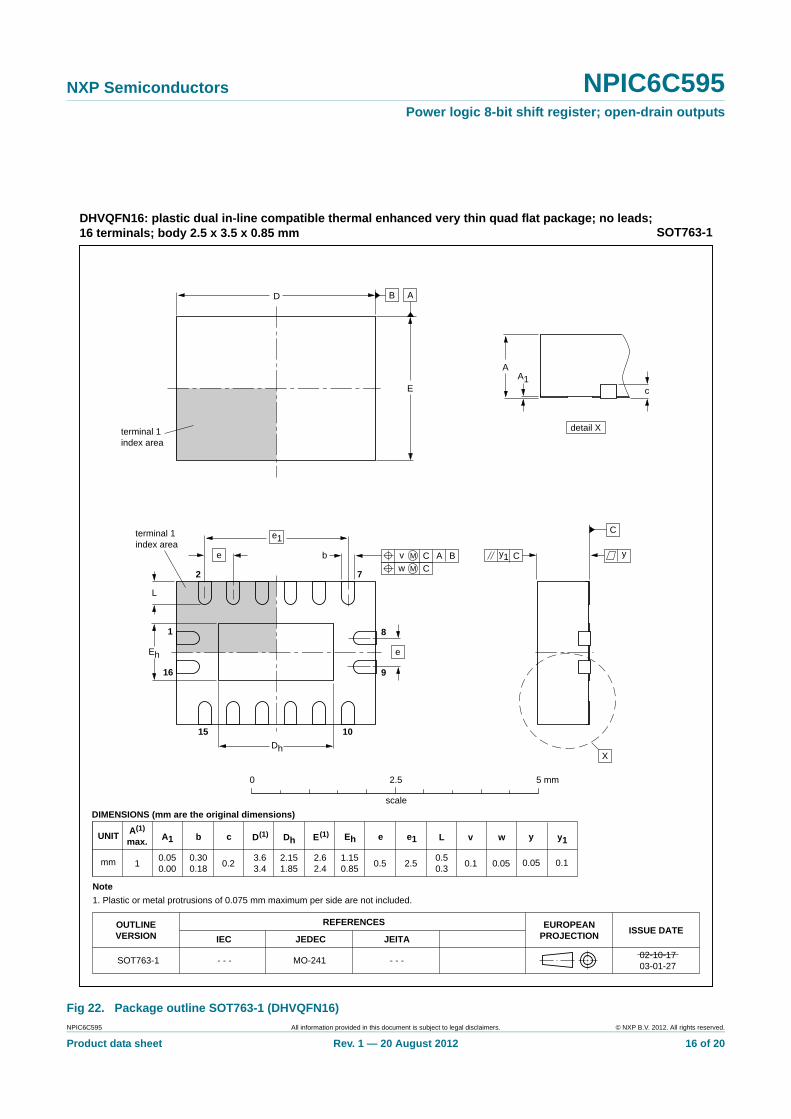
Fig 22. Package outline SOT763-1 (DHVQFN16)
terminal 1index area
0.51
A1 EhbUNIT ye
0.2
c
REFERENCESOUTLINEVERSION
EUROPEANPROJECTION ISSUE DATE
IEC JEDEC JEITA
mm 3.63.4
Dh
2.151.85
y1
2.62.4
1.150.85
e1
2.50.300.18
0.050.00
0.05 0.1
DIMENSIONS (mm are the original dimensions)
SOT763-1 MO-241 - - -- - -
0.50.3
L
0.1
v
0.05
w
0 2.5 5 mm
scale
SOT763-1DHVQFN16: plastic dual in-line compatible thermal enhanced very thin quad flat package; no leads;16 terminals; body 2.5 x 3.5 x 0.85 mm
A(1)
max.
AA1
c
detail X
yy1 Ce
L
Eh
Dh
e
e1
b
2 7
15 10
9
81
16
X
D
E
C
B A
terminal 1index area
ACC
Bv M
w M
E(1)
Note
1. Plastic or metal protrusions of 0.075 mm maximum per side are not included.
D(1)
02-10-1703-01-27
NPIC6C595 All information provided in this document is subject to legal disclaimers. © NXP B.V. 2012. All rights reserved.
Product data sheet Rev. 1 — 20 August 2012 16 of 20

NXP Semiconductors NPIC6C595Power logic 8-bit shift register; open-drain outputs
12. Abbreviations
13. Revision history
Table 10. Abbreviations
Acronym Description
CDM Charged Device Model
CMOS Complementary Metal Oxide Semiconductor
DUT Device Under Test
EDNMOS Extended Drain Negative Metal Oxide Semiconductor
ESD ElectroStatic Discharge
HBM Human Body Model
TTL Transistor-Transistor Logic
Table 11. Revision history
Document ID Release date Data sheet status Change notice Supersedes
NPIC6C595 v.1 20120820 Product data sheet - -
NPIC6C595 All information provided in this document is subject to legal disclaimers. © NXP B.V. 2012. All rights reserved.
Product data sheet Rev. 1 — 20 August 2012 17 of 20
NXP Semiconductors NPIC6C595Power logic 8-bit shift register; open-drain outputs
14. Legal information
14.1 Data sheet status
[1] Please consult the most recently issued document before initiating or completing a design.
[2] The term ‘short data sheet’ is explained in section “Definitions”.
[3] The product status of device(s) described in this document may have changed since this document was published and may differ in case of multiple devices. The latest product status information is available on the Internet at URL http://www.nxp.com.
14.2 Definitions
Draft — The document is a draft version only. The content is still under internal review and subject to formal approval, which may result in modifications or additions. NXP Semiconductors does not give any representations or warranties as to the accuracy or completeness of information included herein and shall have no liability for the consequences of use of such information.
Short data sheet — A short data sheet is an extract from a full data sheet with the same product type number(s) and title. A short data sheet is intended for quick reference only and should not be relied upon to contain detailed and full information. For detailed and full information see the relevant full data sheet, which is available on request via the local NXP Semiconductors sales office. In case of any inconsistency or conflict with the short data sheet, the full data sheet shall prevail.
Product specification — The information and data provided in a Product data sheet shall define the specification of the product as agreed between NXP Semiconductors and its customer, unless NXP Semiconductors and customer have explicitly agreed otherwise in writing. In no event however, shall an agreement be valid in which the NXP Semiconductors product is deemed to offer functions and qualities beyond those described in the Product data sheet.
14.3 Disclaimers
Limited warranty and liability — Information in this document is believed to be accurate and reliable. However, NXP Semiconductors does not give any representations or warranties, expressed or implied, as to the accuracy or completeness of such information and shall have no liability for the consequences of use of such information. NXP Semiconductors takes no responsibility for the content in this document if provided by an information source outside of NXP Semiconductors.
In no event shall NXP Semiconductors be liable for any indirect, incidental, punitive, special or consequential damages (including - without limitation - lost profits, lost savings, business interruption, costs related to the removal or replacement of any products or rework charges) whether or not such damages are based on tort (including negligence), warranty, breach of contract or any other legal theory.
Notwithstanding any damages that customer might incur for any reason whatsoever, NXP Semiconductors’ aggregate and cumulative liability towards customer for the products described herein shall be limited in accordance with the Terms and conditions of commercial sale of NXP Semiconductors.
Right to make changes — NXP Semiconductors reserves the right to make changes to information published in this document, including without limitation specifications and product descriptions, at any time and without notice. This document supersedes and replaces all information supplied prior to the publication hereof.
Suitability for use — NXP Semiconductors products are not designed, authorized or warranted to be suitable for use in life support, life-critical or safety-critical systems or equipment, nor in applications where failure or malfunction of an NXP Semiconductors product can reasonably be expected to result in personal injury, death or severe property or environmental damage. NXP Semiconductors and its suppliers accept no liability for inclusion and/or use of NXP Semiconductors products in such equipment or applications and therefore such inclusion and/or use is at the customer’s own risk.
Applications — Applications that are described herein for any of these products are for illustrative purposes only. NXP Semiconductors makes no representation or warranty that such applications will be suitable for the specified use without further testing or modification.
Customers are responsible for the design and operation of their applications and products using NXP Semiconductors products, and NXP Semiconductors accepts no liability for any assistance with applications or customer product design. It is customer’s sole responsibility to determine whether the NXP Semiconductors product is suitable and fit for the customer’s applications and products planned, as well as for the planned application and use of customer’s third party customer(s). Customers should provide appropriate design and operating safeguards to minimize the risks associated with their applications and products.
NXP Semiconductors does not accept any liability related to any default, damage, costs or problem which is based on any weakness or default in the customer’s applications or products, or the application or use by customer’s third party customer(s). Customer is responsible for doing all necessary testing for the customer’s applications and products using NXP Semiconductors products in order to avoid a default of the applications and the products or of the application or use by customer’s third party customer(s). NXP does not accept any liability in this respect.
Limiting values — Stress above one or more limiting values (as defined in the Absolute Maximum Ratings System of IEC 60134) will cause permanent damage to the device. Limiting values are stress ratings only and (proper) operation of the device at these or any other conditions above those given in the Recommended operating conditions section (if present) or the Characteristics sections of this document is not warranted. Constant or repeated exposure to limiting values will permanently and irreversibly affect the quality and reliability of the device.
Terms and conditions of commercial sale — NXP Semiconductors products are sold subject to the general terms and conditions of commercial sale, as published at http://www.nxp.com/profile/terms, unless otherwise agreed in a valid written individual agreement. In case an individual agreement is concluded only the terms and conditions of the respective agreement shall apply. NXP Semiconductors hereby expressly objects to applying the customer’s general terms and conditions with regard to the purchase of NXP Semiconductors products by customer.
No offer to sell or license — Nothing in this document may be interpreted or construed as an offer to sell products that is open for acceptance or the grant, conveyance or implication of any license under any copyrights, patents or other industrial or intellectual property rights.
Document status[1][2] Product status[3] Definition
Objective [short] data sheet Development This document contains data from the objective specification for product development.
Preliminary [short] data sheet Qualification This document contains data from the preliminary specification.
Product [short] data sheet Production This document contains the product specification.
NPIC6C595 All information provided in this document is subject to legal disclaimers. © NXP B.V. 2012. All rights reserved.
Product data sheet Rev. 1 — 20 August 2012 18 of 20
NXP Semiconductors NPIC6C595Power logic 8-bit shift register; open-drain outputs
Export control — This document as well as the item(s) described herein may be subject to export control regulations. Export might require a prior authorization from competent authorities.
Non-automotive qualified products — Unless this data sheet expressly states that this specific NXP Semiconductors product is automotive qualified, the product is not suitable for automotive use. It is neither qualified nor tested in accordance with automotive testing or application requirements. NXP Semiconductors accepts no liability for inclusion and/or use of non-automotive qualified products in automotive equipment or applications.
In the event that customer uses the product for design-in and use in automotive applications to automotive specifications and standards, customer (a) shall use the product without NXP Semiconductors’ warranty of the product for such automotive applications, use and specifications, and (b) whenever customer uses the product for automotive applications beyond
NXP Semiconductors’ specifications such use shall be solely at customer’s own risk, and (c) customer fully indemnifies NXP Semiconductors for any liability, damages or failed product claims resulting from customer design and use of the product for automotive applications beyond NXP Semiconductors’ standard warranty and NXP Semiconductors’ product specifications.
Translations — A non-English (translated) version of a document is for reference only. The English version shall prevail in case of any discrepancy between the translated and English versions.
14.4 TrademarksNotice: All referenced brands, product names, service names and trademarks are the property of their respective owners.
15. Contact information
For more information, please visit: http://www.nxp.com
For sales office addresses, please send an email to: [email protected]
NPIC6C595 All information provided in this document is subject to legal disclaimers. © NXP B.V. 2012. All rights reserved.
Product data sheet Rev. 1 — 20 August 2012 19 of 20

NXP Semiconductors NPIC6C595Power logic 8-bit shift register; open-drain outputs
16. Contents
1 General description . . . . . . . . . . . . . . . . . . . . . . 1
2 Features and benefits . . . . . . . . . . . . . . . . . . . . 1
3 Applications . . . . . . . . . . . . . . . . . . . . . . . . . . . . 1
4 Ordering information. . . . . . . . . . . . . . . . . . . . . 2
5 Functional diagram . . . . . . . . . . . . . . . . . . . . . . 2
6 Pinning information. . . . . . . . . . . . . . . . . . . . . . 46.1 Pinning . . . . . . . . . . . . . . . . . . . . . . . . . . . . . . . 46.2 Pin description . . . . . . . . . . . . . . . . . . . . . . . . . 4
7 Limiting values. . . . . . . . . . . . . . . . . . . . . . . . . . 57.1 Test circuit and waveform . . . . . . . . . . . . . . . . . 6
8 Recommended operating conditions. . . . . . . . 6
9 Static characteristics. . . . . . . . . . . . . . . . . . . . . 6
10 Dynamic characteristics . . . . . . . . . . . . . . . . . . 810.1 Test circuits and waveforms . . . . . . . . . . . . . . . 8
11 Package outline . . . . . . . . . . . . . . . . . . . . . . . . 14
12 Abbreviations. . . . . . . . . . . . . . . . . . . . . . . . . . 17
13 Revision history. . . . . . . . . . . . . . . . . . . . . . . . 17
14 Legal information. . . . . . . . . . . . . . . . . . . . . . . 1814.1 Data sheet status . . . . . . . . . . . . . . . . . . . . . . 1814.2 Definitions. . . . . . . . . . . . . . . . . . . . . . . . . . . . 1814.3 Disclaimers . . . . . . . . . . . . . . . . . . . . . . . . . . . 1814.4 Trademarks. . . . . . . . . . . . . . . . . . . . . . . . . . . 19
15 Contact information. . . . . . . . . . . . . . . . . . . . . 19
16 Contents . . . . . . . . . . . . . . . . . . . . . . . . . . . . . . 20
© NXP B.V. 2012. All rights reserved.
For more information, please visit: http://www.nxp.comFor sales office addresses, please send an email to: [email protected]
Date of release: 20 August 2012
Document identifier: NPIC6C595
Please be aware that important notices concerning this document and the product(s)described herein, have been included in section ‘Legal information’.