
1 COMBINATIONAL LOGIC One or more digital signal inputs One or more digital signal outputs Outputs...
26
1 COMBINATIONAL LOGIC • One or more digital signal inputs • One or more digital signal outputs • Outputs are only functions of current input values (ideal) plus logic propagation delays Combination al Logic I 1 I m O 1 O n
-
Upload
clarence-hodges -
Category
Documents
-
view
217 -
download
0
Transcript of 1 COMBINATIONAL LOGIC One or more digital signal inputs One or more digital signal outputs Outputs...

1
COMBINATIONAL LOGIC
• One or more digital signal inputs• One or more digital signal outputs• Outputs are only functions of current input values
(ideal) plus logic propagation delays
Combinational Logic
I1
Im
O1
On
2
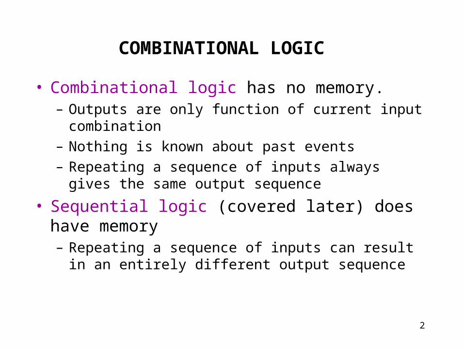
COMBINATIONAL LOGIC
• Combinational logic has no memory.– Outputs are only function of current input combination
– Nothing is known about past events
– Repeating a sequence of inputs always gives the same output sequence
• Sequential logic (covered later) does have memory– Repeating a sequence of inputs can result in an entirely
different output sequence
3
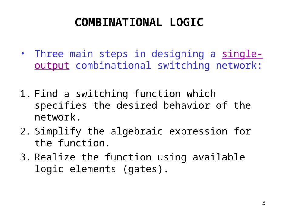
COMBINATIONAL LOGIC
• Three main steps in designing a single-output combinational switching network:
1. Find a switching function which specifies the desired behavior of the network.
2. Simplify the algebraic expression for the function.
3. Realize the function using available logic elements (gates).
4
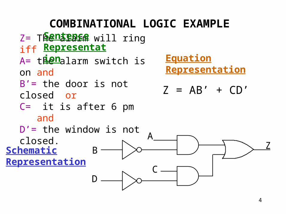
COMBINATIONAL LOGIC EXAMPLE
B
D
ZSchematicRepresentation
Z= The alarm will ring iffA= the alarm switch is on andB’= the door is not closed orC= it is after 6 pm andD’= the window is not closed.
Sentence Representation
A
C
EquationRepresentation
Z = AB’ + CD’

5
DESIGN USING TRUTH TABLE
Example:
ABC represents a 3-bit binary number e.g. 011 = 3, 101 = 5
Output F is 1 if ABC >= 011 and is 0 if ABC < 011
A B C F 0 0 0 0 0 0 1 0 0 1 0 0 0 1 1 1 1 0 0 1 1 0 1 1 1 1 0 1 1 1 1 1
The ‘1’s represent F(A,B,C).
The ‘0’s represent F’(A,B,C)

6
EXAMPLE Cont’d: TRUTH TABLE TO SOP FORM
Can write SOP form of equation directly from truth table.
A B C F 0 0 0 0 0 0 1 0 0 1 0 0 0 1 1 1 1 0 0 1 1 0 1 1 1 1 0 1 1 1 1 1
A’BCAB’C’AB’CABC’ABC
F(A,B,C) = A’BC + AB’C’ + AB’C + ABC’ + ABC
= A’BC + AB’ + AB = A’BC + A = A + BC
Note that each term in F has ALL variables present. If a product term has ALL
variables present, it is a MINTERM.
FB
CA

7
TRUTH TABLE TO POS FORM
To get POS form of F, write SOP form of F’, then use DeMorgan’s Law.
A B C F 0 0 0 0 0 0 1 0 0 1 0 0 0 1 1 1 1 0 0 1 1 0 1 1 1 1 0 1 1 1 1 1
A’B’C’A’B’CA’BC’
F’(A,B,C) = A’B’C’ + A’B’C + A’BC’ Take complement of both sides:
(F’(A,B,C))’ = (A’B’C’ + A’B’C + A’BC’)’
Apply DeMorgan’s Law to right side. Left side is (F’)’ = F.
F(A,B,C) = (A’B’C’)’ (A’B’C)’ (A’BC’)’
Apply DeMorgan’s Law to each term F(A,B,C) = (A+B+C)(A+B+C’)(A+B’+C)
which is in POS Form.

8
MINTERMS, MAXTERMSWe saw that:
F(A,B,C) = (A+B+C) (A+B+C’)(A+B’+C)
F(A,B,C) = A’BC + AB’C’ + AB’C + ABC’ + ABC’ + ABC
SOP form. If a product term has all variables present (each occurring exactly once, in complemented or uncomplemented form, but not both), it is a MINTERM.
POS form. If a sum term has all variables present (each occurring exactly once, in complemented or uncomplemented form, but not both), it is a MAXTERM.
All Boolean functions can be written in terms of either Minterms or Maxterms.
9
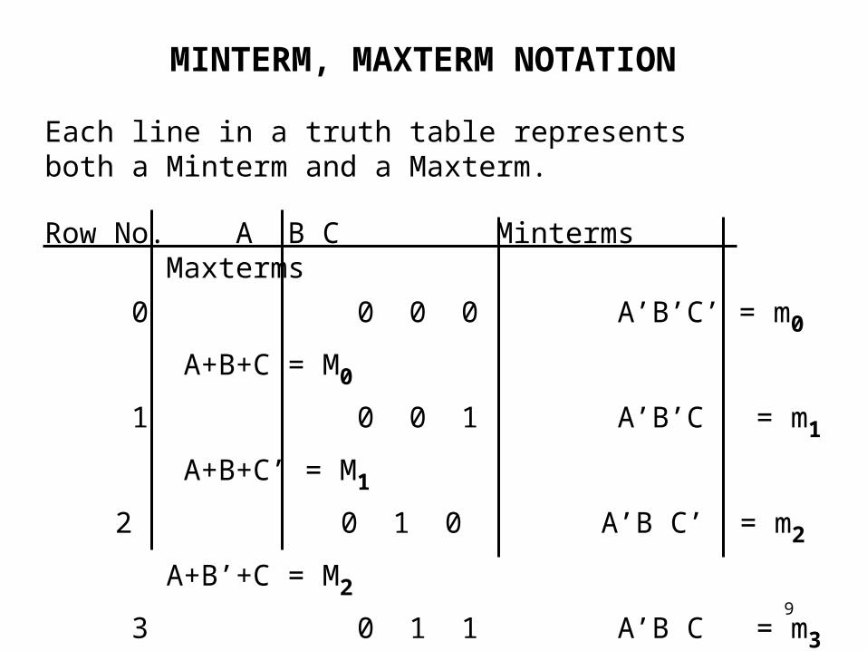
MINTERM, MAXTERM NOTATION
Each line in a truth table represents both a Minterm and a Maxterm.
Row No. A B C Minterms Maxterms
0 0 0 0 A’B’C’ = m0 A+B+C = M0
1 0 0 1 A’B’C = m1 A+B+C’ = M1
2 0 1 0 A’B C’ = m2 A+B’+C = M2
3 0 1 1 A’B C = m3 A+B’+C’ = M3
4 1 0 0 A B’C’ = m4 A’+B+C = M4
5 1 0 1 A B’C = m5 A’+B+C’= M5
6 1 1 0 A B C’ = m6 A’+B’+C = M6
7 1 1 1 A B C = m7 A’+B’+C’= M7

10
USING MINTERMS, MAXTERMS
A boolean function can be written in terms of Minterm or Maxterm notation as a shorthand method of specifying the function.
F(A,B,C) = A’BC + AB’C’ + AB’C + ABC’ + ABC’ + ABC
= m3 + m4 + m5 + m6 + m7
= m(3,4,5,6,7)
F(A,B,C) = (A+B+C) (A+B+C’)(A+B’+C)
= M0 M1 M2
= M(0,1,2)
Minterms correspond to ‘1’s of F, Maxterms correspond to ‘0’s of F in truth table.

11
FROM MINTERMS TO TRUTH TABLE
Minterms correspond to ‘1’s in Truth table
F(A,B,C) = m(1,2,6) = m1 + m2 + m6
= A’B’C + A’BC’ + ABC’ A B C F 0 0 0 0 0 0 1 1 0 1 0 1 0 1 1 0 1 0 0 0 1 0 1 0 1 1 0 1 1 1 1 0
m1m2
m6
12
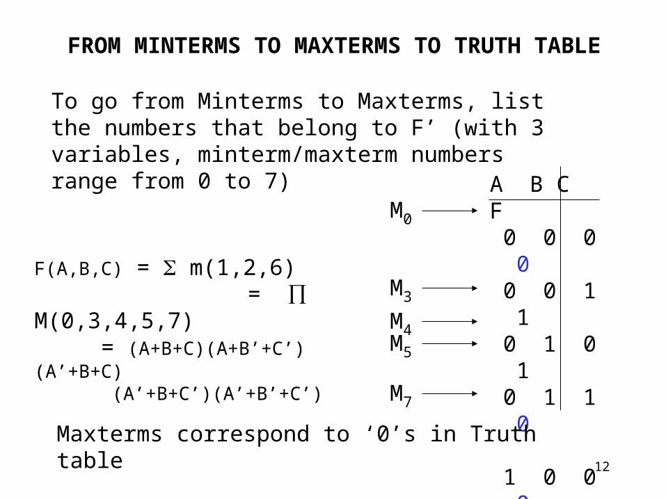
FROM MINTERMS TO MAXTERMS TO TRUTH TABLE
To go from Minterms to Maxterms, list the numbers that belong to F’ (with 3 variables, minterm/maxterm numbers range from 0 to 7)
F(A,B,C) = m(1,2,6) = M(0,3,4,5,7) = (A+B+C)(A+B’+C’)(A’+B+C) (A’+B+C’)(A’+B’+C’)
A B C F 0 0 0 0 0 0 1 1 0 1 0 1 0 1 1 0 1 0 0 0 1 0 1 0 1 1 0 1 1 1 1 0
M0
M3
M4M5
M7
Maxterms correspond to ‘0’s in Truth table
13
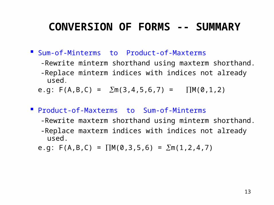
CONVERSION OF FORMS -- SUMMARY
Sum-of-Minterms to Product-of-Maxterms
-Rewrite minterm shorthand using maxterm shorthand.
-Replace minterm indices with indices not already used.
e.g: F(A,B,C) = m(3,4,5,6,7) = M(0,1,2)
Product-of-Maxterms to Sum-of-Minterms
-Rewrite maxterm shorthand using minterm shorthand.
-Replace maxterm indices with indices not already used.e.g: F(A,B,C) = M(0,3,5,6) = m(1,2,4,7)
14
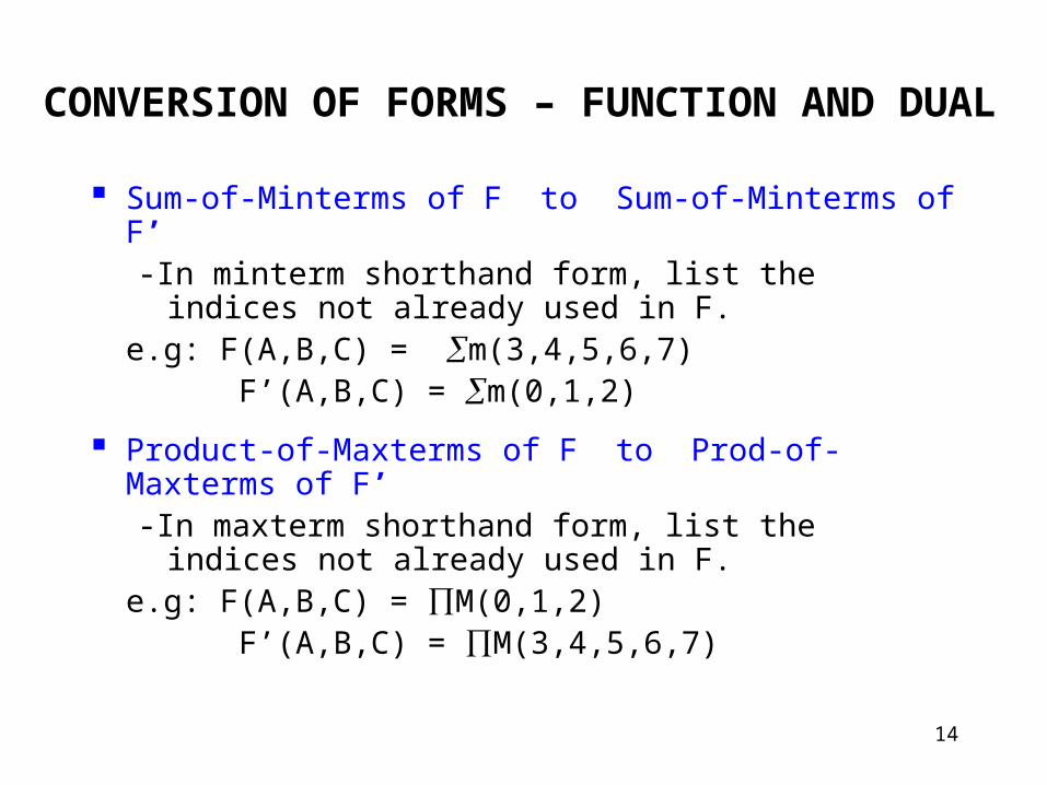
CONVERSION OF FORMS – FUNCTION AND DUAL
Sum-of-Minterms of F to Sum-of-Minterms of F’ -In minterm shorthand form, list the indices not already
used in F.e.g: F(A,B,C) = m(3,4,5,6,7) F’(A,B,C) = m(0,1,2)
Product-of-Maxterms of F to Prod-of-Maxterms of F’-In maxterm shorthand form, list the indices not already
used in F.e.g: F(A,B,C) = M(0,1,2) F’(A,B,C) = M(3,4,5,6,7)

15
Sum-of-Minterms of F to Product-of-Maxterms of F’-Rewrite in maxterm shorthand form, using the same
indices as in F.e.g: F(A,B,C) = m(3,4,5,6,7) F’(A,B,C) = M(3,4,5,6,7)
Product-of-Maxterms of F to Sum-of-Minterms of F’-Rewrite in minterm shorthand form, using the same
indices as in F.
e.g: F(A,B,C) = M(0,1,2) F’(A,B,C) = m(0,1,2)
CONVERSION OF FORMS – FUNCTION AND DUAL
16
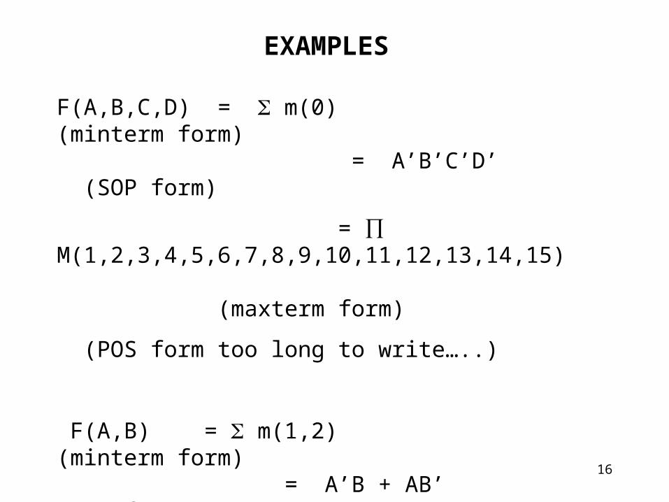
EXAMPLES
F(A,B,C,D) = m(0) (minterm form) = A’B’C’D’ (SOP form)
= M(1,2,3,4,5,6,7,8,9,10,11,12,13,14,15) (maxterm form)
(POS form too long to write…..)
F(A,B) = m(1,2) (minterm form) = A’B + AB’ (SOP form) = M(0,3) (maxterm form) = (A+B)(A’+B’) (POS form)
17
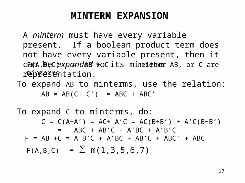
MINTERM EXPANSION
A minterm must have every variable present. If a boolean product term does not have every variable present, then it can be expanded to its minterm representation.F(A,B,C) = AB + C neither AB, or C are minterms
To expand AB to minterms, use the relation:AB = AB(C+ C’) = ABC + ABC’
To expand C to minterms, do:C = C(A+A’) = AC+ A’C = AC(B+B’) + A’C(B+B’) = ABC + AB’C + A’BC + A’B’C
F = AB +C = A’B’C + A’BC + AB’C + ABC’ + ABC
F(A,B,C) = m(1,3,5,6,7)

18
MAXTERM EXPANSION
A maxterm must have every variable present. If a boolean sum term does not have every variable present, then it can be expanded to its maxterm representation.
F(A,B,C) = (A+B) (C) neither (A+B), or C are maxterms
To expand (A+B) to maxterms, use the relation:(A+B) = (A+B+C’C) = (A+B+C’)(A+B+C)
To expand C to maxterms, do:C = C+A’A = (A’+C)(A+C) = (A’+C +BB’)(A+C+BB’) = (A’+B’+C)(A’+B+C)(A+B’+C)(A+B+C)
F = (A+B)(C) = (A+B+C)(A+B+C’)(A+B’+C)(A’+B+C)(A’+B’+C)
F(A,B,C) = M(0,1,2,4,6)
19
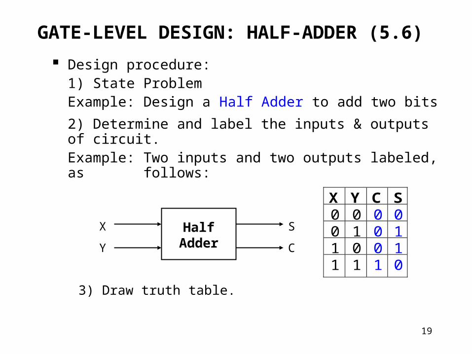
Design procedure:1) State Problem
Example: Design a Half Adder to add two bits
2) Determine and label the inputs & outputs of circuit.Example: Two inputs and two outputs labeled, as
follows:
HalfAdder
X
Y
S
C
3) Draw truth table.
X Y C S 0 0 0 0 0 1 0 1 1 0 0 1 1 1 1 0
GATE-LEVEL DESIGN: HALF-ADDER (5.6)

20
GATE-LEVEL DESIGN: HALF-ADDER (Cont’d)
4) Obtain simplified Boolean function.
Example: C = XY S = X'Y + XY' = XY
XY
S
C
Half Adder
5) Draw logic diagram.
X Y C S 0 0 0 0 0 1 0 1 1 0 0 1 1 1 1 0

21
GATE-LEVEL DESIGN: FULL-ADDER
Half-adder adds up only two bits.
To add two binary numbers, we need to add 3 bits (including the carry).
Example: 1 1 1 carry0 0 1 1 X
+ 0 1 1 1 Y1 0 1 0 S
Need Full Adder (so called as it can be made from two half-adders).
FullAdder
XYZ
S
C
Z - carry in (to the current position) C - carry out (to the next position)

22
GATE-LEVEL DESIGN: FULL-ADDER (Cont’d)
Truth table:
X Y Z C S 0 0 0 0 0 0 0 1 0 1 0 1 0 0 1 0 1 1 1 0 1 0 0 0 1 1 0 1 1 0 1 1 0 1 0 1 1 1 1 1
S = m(1,2,4,7)
= X'Y'Z + X'YC' + XY'Z' + XYZ
= X'(Y'Z + YZ') + X(Y'Z' + YZ)= X'(YZ) + X(YZ)'= X(YZ) = (XY)Z
C = m(3,5,6,7) = X'YZ+XY'Z+XYZ'+ XYZ
= X'YZ+XY'Z+XYZ'+XYZ +XYZ+XYZ
=(X'YZ+XYZ)+(XY'Z+XYZ)+(XYZ'+XYZ)
= YZ + XZ + XY (adjacency) = XY + XZ + YZ = XY + (X + Y)Z = XY + ((XY) + XY)Z = XY + (XY)Z + XYZ = XY + (XY)Z
23
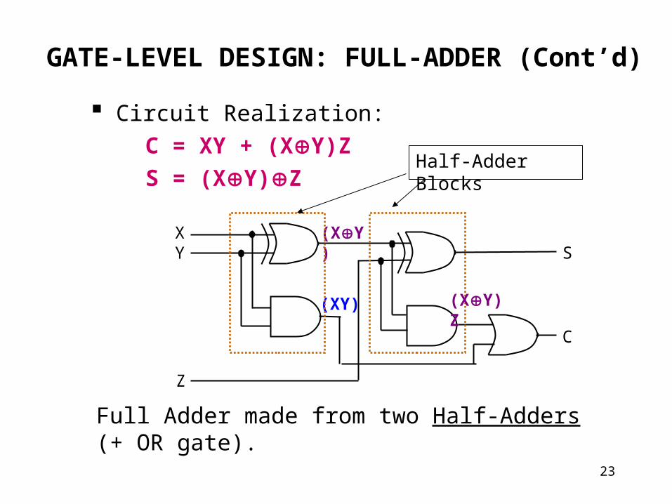
GATE-LEVEL DESIGN: FULL-ADDER (Cont’d)
Circuit Realization:
C = XY + (XY)Z
S = (XY)Z
Full Adder made from two Half-Adders (+ OR gate).
(XY)XY S
C
Z
(XY) (XY)Z
Half-Adder Blocks
24
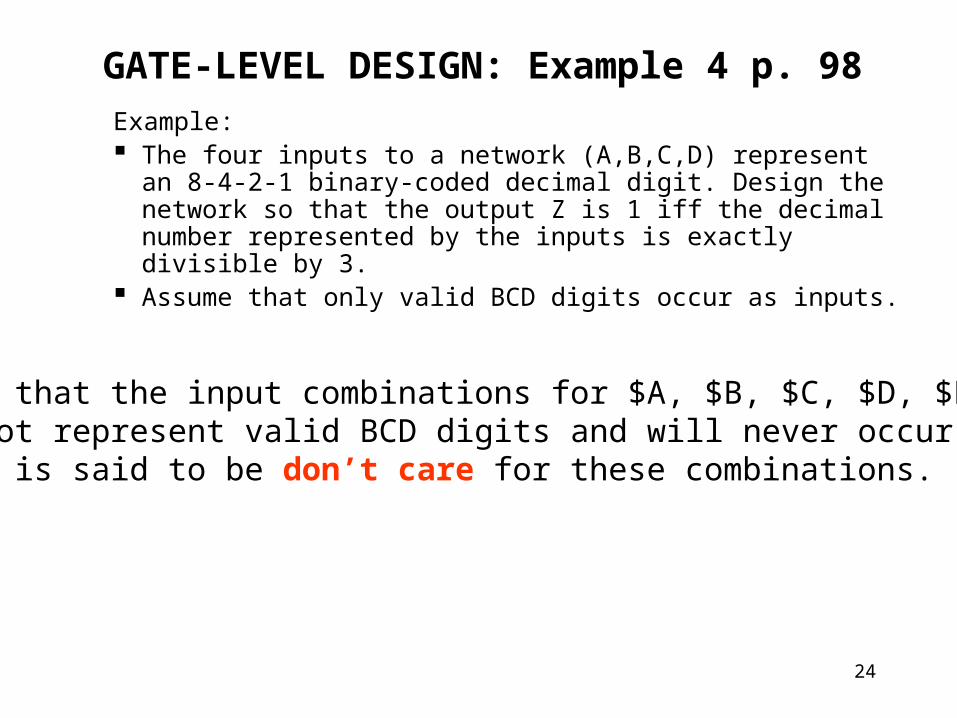
GATE-LEVEL DESIGN: Example 4 p. 98
Example: The four inputs to a network (A,B,C,D) represent an 8-4-
2-1 binary-coded decimal digit. Design the network so that the output Z is 1 iff the decimal number represented by the inputs is exactly divisible by 3.
Assume that only valid BCD digits occur as inputs.
Note that the input combinations for $A, $B, $C, $D, $E, $Fdo not represent valid BCD digits and will never occur.-- Z is said to be don’t care for these combinations.

25
GATE-LEVEL DESIGN: Example 4 p.98
A0000000011111111
B0000111100001111
C0011001100110011
D0101010101010101
Z1001001010XXXXXX
#0123456789ABCDEF
Z = m(0,3,6,9)
+ d(10,11,12,13,14,15)
In order to find the simplest network which will realize Z, we must choose some of the don’t cares (X’s) to be 0 and someto be 1.The easiest way to do this is with aKarnaugh map …… next chapter.
26
What do you need to Know?
Combinational Network Design -- Problem Statement to Truth Table to Boolean Eqn. to
Gate Network• Minterm, Maxterm definitions• Truth table to Minterms, vice versa• Truth table to Maxterms, vice versa• Conversion of Standard Forms SOP to POS vice versa• Minterm, Maxterm Expansions• Gate-Level Design using Truth Table e.g. Full Adder• Incompletely Specified Functions i.e. don’t care conditions


![ECE-V-DIGITAL SIGNAL PROCESSING [10EC52] …vtusolution.in/.../digital-signal-processing-10ec52.pdfDigital vtusolution.in Signal Processing 10EC52 TEXT BOOK: 1. DIGITAL SIGNAL PROCESSING](https://static.fdocuments.in/doc/165x107/5afe42bb7f8b9a256b8ccd2e/ece-v-digital-signal-processing-10ec52-signal-processing-10ec52-text-book.jpg)


