NI 6229 Device Specifications - National · PDF fileDEVICE SPECIFICATIONS NI 6229 M Series...
22
DEVICE SPECIFICATIONS NI 6229 M Series Data Acquisition: 16-Bit, 250 kS/s, 32 AI, 48 DIO, 4 AO The following specifications are typical at 25 °C, unless otherwise noted. For more information about the NI 6229, refer to the M Series User Manual available at ni.com/ manuals. Analog Input Number of channels 16 differential or 32 single ended ADC resolution 16 bits DNL No missing codes guaranteed INL Refer to the AI Absolute Accuracy section Sample rate Single channel maximum 250 kS/s Multichannel maximum (aggregate) 250 kS/s Minimum No minimum Timing accuracy 50 ppm of sample rate Timing resolution 50 ns Input coupling DC Input range ±0.2 V, ±1 V, ±5 V, ±10 V Maximum working voltage for analog inputs (signal + common mode) ±11 V of AI GND CMRR (DC to 60 Hz) 92 dB Input impedance Device on AI+ to AI GND >10 GΩ in parallel with 100 pF AI- to AI GND >10 GΩ in parallel with 100 pF
Transcript of NI 6229 Device Specifications - National · PDF fileDEVICE SPECIFICATIONS NI 6229 M Series...
DEVICE SPECIFICATIONS
NI 6229M Series Data Acquisition: 16-Bit, 250 kS/s, 32 AI, 48 DIO, 4 AO
The following specifications are typical at 25 °C, unless otherwise noted. For moreinformation about the NI 6229, refer to the M Series User Manual available at ni.com/manuals.
Analog InputNumber of channels 16 differential or 32 single ended
ADC resolution 16 bits
DNL No missing codes guaranteed
INL Refer to the AI Absolute Accuracy section
Sample rate
Single channel maximum 250 kS/s
Multichannel maximum (aggregate) 250 kS/s
Minimum No minimum
Timing accuracy 50 ppm of sample rate
Timing resolution 50 ns
Input coupling DC
Input range ±0.2 V, ±1 V, ±5 V, ±10 V
Maximum working voltage for analoginputs (signal + common mode)
±11 V of AI GND
CMRR (DC to 60 Hz) 92 dB
Input impedance
Device on
AI+ to AI GND >10 GΩ in parallel with 100 pF
AI- to AI GND >10 GΩ in parallel with 100 pF
Device off
AI+ to AI GND 820 Ω
AI- to AI GND 820 Ω
Input bias current ±100 pA
Crosstalk (at 100 kHz)
Adjacent channels -75 dB
Non-adjacent channels -90 dB
Small signal bandwidth (-3 dB) 700 kHz
Input FIFO size 4,095 samples
Scan list memory 4,095 entries
Data transfers
PCI/PXI DMA (scatter-gather), interrupts,programmed I/O
USB USB Signal Stream, programmed I/O
Overvoltage protection for all analog input and sense channels
Device on ±25 V for up to two AI pins
Device off ±15 V for up to two AI pins
Input current during overvoltage condition ±20 mA maximum/AI pin
Settling Time for Multichannel MeasurementsAccuracy, full-scale step, all ranges
±90 ppm of step (±6 LSB) 4 μs convert interval
±30 ppm of step (±2 LSB) 5 μs convert interval
±15 ppm of step (±1 LSB) 7 μs convert interval
2 | ni.com | NI 6229 Device Specifications
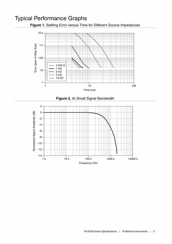
Typical Performance GraphsFigure 1. Settling Error versus Time for Different Source Impedances
1
10
100
1 k
10 k
110 100
1 kΩ2 kΩ5 kΩ10 kΩ
≤100 Ω
Err
or (
ppm
of S
tep
Siz
e)
Time (ms)
Figure 2. AI Small Signal Bandwidth
1 k 10 k 100 k 1000 k 10000 k
Frequency (Hz)
Nor
mal
ized
Sig
nal A
mpl
itude
(dB
)
–14
–12
–10
–8
–6
–4
–2
0
2
NI 6229 Device Specifications | © National Instruments | 3
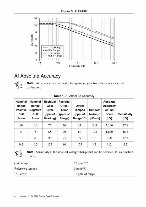
Figure 3. AI CMRR
0
20
40
60
80
100
120
10 100 1 k 10 k 100 kFrequency (Hz)
CM
RR
(dB
)
10 V Range5 V Range1 V Range0.2 V Range
AI Absolute AccuracyNote Accuracies listed are valid for up to one year from the device externalcalibration.
Table 1. AI Absolute Accuracy
NominalRange
PositiveFull
Scale
NominalRange
NegativeFull
Scale
ResidualGainError
(ppm ofReading)
ResidualOffsetError
(ppm ofRange)
OffsetTempco(ppm of
Range/°C)
RandomNoise, σ(μVrms)
AbsoluteAccuracy
at FullScale(μV)
Sensitivity(μV)
10 -10 75 20 57 244 3,100 97.6
5 -5 85 20 60 122 1,620 48.8
1 -1 95 25 79 30 360 12.0
0.2 -0.2 135 80 175 13 112 5.2
Note Sensitivity is the smallest voltage change that can be detected. It is a functionof noise.
Gain tempco 25 ppm/°C
Reference tempco 5 ppm/°C
INL error 76 ppm of range
4 | ni.com | NI 6229 Device Specifications
AI Absolute Accuracy EquationAbsoluteAccuracy = Reading · (GainError) + Range · (OffsetError) + NoiseUncertainty
GainError = ResidualAIGainError + GainTempco · (TempChangeFromLastInternalCal)+ ReferenceTempco · (TempChangeFromLastExternalCal)OffsetError = ResidualAIOffsetError + OffsetTempco ·(TempChangeFromLastInternalCal) + INLError
NoiseUncertainty = RandomNoise ⋅ 3100 for a coverage factor of 3 σ and averaging
100 points.
AI Absolute Accuracy ExampleAbsolute accuracy at full scale on the analog input channels is determined using the followingassumptions:• TempChangeFromLastExternalCal = 10 °C• TempChangeFromLastInternalCal = 1 °C• number_of_readings = 100• CoverageFactor = 3 σ
For example, on the 10 V range, the absolute accuracy at full scale is as follows:GainError = 75 ppm + 25 ppm · 1 + 5 ppm · 10 = 150 ppmOffsetError = 20 ppm + 57 ppm · 1 + 76 ppm = 153 ppm
NoiseUncertainty = 244 µ� ⋅ 3100 = 73 µV
AbsoluteAccuracy = 10 V · (GainError) + 10 V · (OffsetError) + NoiseUncertainty =3,100 µV
Analog OutputNumber of channels 4
DAC resolution 16 bits
DNL ±1 LSB
Monotonicity 16 bit guaranteed
Maximum update rate
1 channel 833 kS/s
2 channels 740 kS/s per channel
3 channels 666 kS/s per channel
4 channels 625 kS/s per channel
Timing accuracy 50 ppm of sample rate
NI 6229 Device Specifications | © National Instruments | 5
Timing resolution 50 ns
Output range ±10 V
Output coupling DC
Output impedance 0.2 Ω
Output current drive ±5 mA
Overdrive protection ±25 V
Overdrive current 10 mA
Power-on state ±20 mV1
Power-off glitch 400 mV for 200 ms
Output FIFO size 8,191 samples shared among channels used
Data transfers
PCI/PXI DMA (scatter-gather), interrupts,programmed I/O
USB USB Signal Stream, programmed I/O
AO waveform modes Non-periodic waveform, periodic waveformregeneration mode from onboard FIFO,periodic waveform regeneration from hostbuffer including dynamic update
Settling time, full-scale step,15 ppm (1 LSB)
6 µs
Slew rate 15 V/µs
Glitch energy
Magnitude 100 mV
Duration 2.6 µs
AO Absolute AccuracyAbsolute accuracy at full-scale numbers is valid immediately following internal calibrationand assumes the device is operating within 10 °C of the last external calibration.
Note Accuracies listed are valid for up to one year from the device externalcalibration.
1 When the USB Screw Terminal device is powered on, the analog output signal is not defined untilafter USB configuration is complete.
6 | ni.com | NI 6229 Device Specifications
Table 2. AO Absolute Accuracy
NominalRange
PositiveFull Scale
NominalRange
NegativeFull Scale
ResidualGain Error
(ppm ofReading)
GainTempco(ppm/°C)
ResidualOffset
Error (ppmof Range)
OffsetTempco(ppm of
Range/°C)
AbsoluteAccuracy
at FullScale (μV)
10 -10 90 10 40 5 3,230
Reference tempco 5 ppm/°C
INL error 128 ppm of range
AO Absolute Accuracy EquationAbsoluteAccuracy = OutputValue · (GainError) + Range · (OffsetError)
GainError = ResidualGainError + GainTempco · (TempChangeFromLastInternalCal) +ReferenceTempco · (TempChangeFromLastExternalCal)OffsetError = ResidualOffsetError + AOOffsetTempco ·(TempChangeFromLastInternalCal) + INLError
Digital I/O/PFI
Static CharacteristicsNumber of channels 48 total, 32 (P0.<0..31>),
16 (PFI <0..7>/P1, PFI <8..15>/P2)
Ground reference D GND
Direction control Each terminal individually programmable asinput or output
Pull-down resistor 50 kΩ typical, 20 kΩ minimum
Input voltage protection ±20 V on up to two pins2
Waveform Characteristics (Port 0 Only)Terminals used Port 0 (P0.<0..31>)
Port/sample size Up to 32 bits
Waveform generation (DO) FIFO 2,047 samples
Waveform acquisition (DI) FIFO 2,047 samples
2 Stresses beyond those listed under Input voltage protection may cause permanent damage to thedevice.
NI 6229 Device Specifications | © National Instruments | 7
DI or DO Sample Clock frequency 0 MHz to 1 MHz, system and bus activitydependent
Data transfers
PCI/PXI DMA (scatter-gather), interrupts,programmed I/O
USB USB Signal Stream, programmed I/O
DI or DO Sample Clock source3 Any PFI, RTSI, AI Sample or Convert Clock,AO Sample Clock, Ctr n Internal Output, andmany other signals
PFI/Port 1/Port 2 FunctionalityFunctionality Static digital input, static digital output,
timing input, timing output
Timing output sources Many AI, AO, counter, DI, DO timing signals
Debounce filter settings 125 ns, 6.425 µs, 2.56 ms, disable; high andlow transitions; selectable per input
Recommended Operating Conditions
Table 3. PCI/PXI
Level Minimum Maximum
Input high voltage (VIH) 2.2 V 5.25 V
Input low voltage (VIL) 0 V 0.8 V
Output high current (IOH) P0.<0..31> — -24 mA
Output high current (IOH) PFI <0..15>/P1/P2 — -16 mA
Output low current (IOL) P0.<0..31> — 24 mA
Output low current (IOL) PFI <0..15>/P1/P2 -— 16 mA
Table 4. USB Devices
Level Minimum Maximum
Input high voltage (VIH) 2.2 V 5.25 V
Input low voltage (VIL) 0 V 0.8 V
3 The digital subsystem does not have its own dedicated internal timing engine. Therefore, a sampleclock must be provided from another subsystem on the device or an external source.
8 | ni.com | NI 6229 Device Specifications
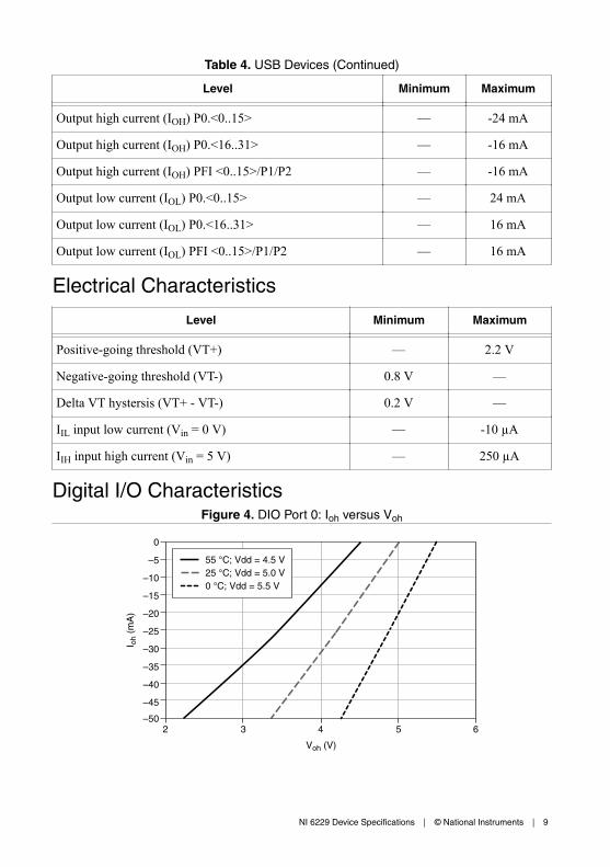
Table 4. USB Devices (Continued)
Level Minimum Maximum
Output high current (IOH) P0.<0..15> — -24 mA
Output high current (IOH) P0.<16..31> — -16 mA
Output high current (IOH) PFI <0..15>/P1/P2 — -16 mA
Output low current (IOL) P0.<0..15> — 24 mA
Output low current (IOL) P0.<16..31> — 16 mA
Output low current (IOL) PFI <0..15>/P1/P2 — 16 mA
Electrical Characteristics
Level Minimum Maximum
Positive-going threshold (VT+) — 2.2 V
Negative-going threshold (VT-) 0.8 V —
Delta VT hystersis (VT+ - VT-) 0.2 V —
IIL input low current (Vin = 0 V) — -10 µA
IIH input high current (Vin = 5 V) — 250 µA
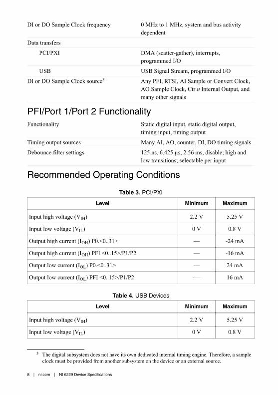
Digital I/O CharacteristicsFigure 4. DIO Port 0: Ioh versus Voh
–50
–45
–40
–35
–30
–25
–20
–15
–10
–5
0
2 3 4 5 6
Voh (V)
I oh
(mA
)
55 °C; Vdd = 4.5 V25 °C; Vdd = 5.0 V0 °C; Vdd = 5.5 V
NI 6229 Device Specifications | © National Instruments | 9
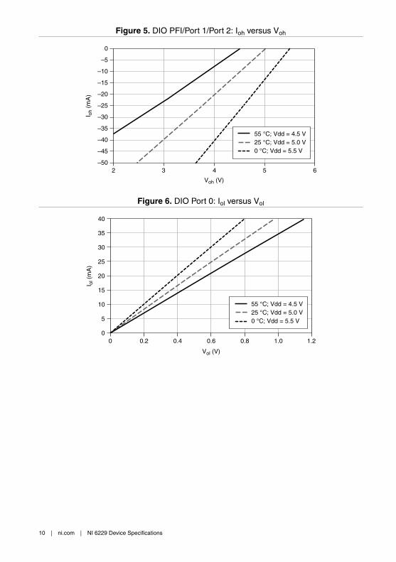
Figure 5. DIO PFI/Port 1/Port 2: Ioh versus Voh
–50
–45
–40
–35
–30
–25
–20
–15
–10
–5
0
2 3 4 5 6
Voh (V)
I oh
(mA
)
55 °C; Vdd = 4.5 V25 °C; Vdd = 5.0 V0 °C; Vdd = 5.5 V
Figure 6. DIO Port 0: Iol versus Vol
0
5
10
15
20
25
30
35
40
0 0.2 0.4 0.6 0.8 1.0 1.2
Vol (V)
I ol (
mA
)
55 °C; Vdd = 4.5 V25 °C; Vdd = 5.0 V0 °C; Vdd = 5.5 V
10 | ni.com | NI 6229 Device Specifications
Figure 7. DIO PFI/Port 1/Port 2: Iol versus Vol
0
5
10
15
20
25
30
35
40
0 0.2 0.4 0.6 0.8 1.0 1.2
Vol (V)
I ol (
mA
)
55 °C; Vdd = 4.5 V25 °C; Vdd = 5.0 V0 °C; Vdd = 5.5 V
General-Purpose Counters/TimersNumber of counter/timers 2
Resolution 32 bits
Counter measurements Edge counting, pulse, semi-period, period,two-edge separation
Position measurements X1, X2, X4 quadrature encoding withChannel Z reloading; two-pulse encoding
Output applications Pulse, pulse train with dynamic updates,frequency division, equivalent time sampling
Internal base clocks 80 MHz, 20 MHz, 0.1 MHz
External base clock frequency 0 MHz to 20 MHz
Base clock accuracy 50 ppm
Inputs Gate, Source, HW_Arm, Aux, A, B, Z,Up_Down
Routing options for inputs Any PFI, RTSI, PXI_TRIG, PXI_STAR,analog trigger, many internal signals
FIFO 2 samples
Data transfers
PCI/PXI Dedicated scatter-gather DMA controller foreach counter/timer; interrupts, programmed I/O
USB USB Signal Stream, programmed I/O
NI 6229 Device Specifications | © National Instruments | 11
Frequency GeneratorNumber of channels 1
Base clocks 10 MHz, 100 kHz
Divisors 1 to 16
Base clock accuracy 50 ppm
Output can be available on any output PFI or RTSI terminal.
Phase-Locked Loop (PLL)Note PCI/PXI devices only.
Number of PLLs 1
Reference signal PXI_STAR, PXI_CLK10, RTSI <0..7>
Output of PLL 80 MHz Timebase; other signals derived from80 MHz Timebase including 20 MHz and100 kHz Timebases
External Digital TriggersSource Any PFI, RTSI, PXI_TRIG, PXI_STAR
Polarity Software-selectable for most signals
Analog input function Start Trigger, Reference Trigger,Pause Trigger, Sample Clock, Convert Clock,Sample Clock Timebase
Analog output function Start Trigger, Pause Trigger, Sample Clock,Sample Clock Timebase
Counter/timer function Gate, Source, HW_Arm, Aux, A, B, Z,Up_Down
Digital waveform generation (DO)function
Sample Clock
Digital waveform acquisition (DI)function
Sample Clock
12 | ni.com | NI 6229 Device Specifications
Device-to-Device Trigger BusPCI RTSI <0..7>4
PXI PXI_TRIG <0..7>, PXI_STAR
USB source None
Output selections 10 MHz Clock, frequency generator output,many internal signals
Debounce filter settings 125 ns, 6.425 μs, 2.56 ms, disable; high andlow transitions; selectable per input
Bus InterfacePCI/PXI 3.3 V or 5 V signal environment
USB USB 2.0 Hi-Speed or full-speed5, 6
DMA channels (PCI/PXI) 6, can be used for analog input, analog output,digital input, digital output, counter/timer 0,counter/timer 1
USB Signal Stream 4, can be used for analog input, analog output,counter/timer 0, counter/timer 1
The PXI device supports one of the following features:• May be installed in PXI Express hybrid slots• Or, may be used to control SCXI in PXI/SCXI combo chassis
Table 5. PXI/SCXI Combo and PXI Express Chassis Compatibility
M Series Part NumberSCXI Control in PXI/SCXI
Combo ChassisPXI Express Hybrid Slot
Compatible
191332B-01 No Yes
191332B-11 Yes No
191322A-0x Yes No
4 In other sections of this document, RTSI refers to RTSI <0..7> for the PCI devices orPXI_TRIG <0..7> for PXI devices.
5 If you are using an USB M Series device in full-speed mode, device performance will be lower andyou will not be able to achieve maximum sample/update rates.
6 Operating on a full-speed bus may result in lower performance.
NI 6229 Device Specifications | © National Instruments | 13
Power RequirementsCurrent draw from bus during no-load condition7
+5 V 0.02 A
+3.3 V 0.25 A
+12 V 0.15 A
Current draw from bus during AI and AO overvoltage condition7
+5 V 0.02 A
+3.3 V 0.25 A
+12 V 0.25 A
Caution USB devices must be powered with an NI offered AC adapter or aNational Electric Code (NEC) Class 2 DC source that meets the power requirementsfor the device and has appropriate safety certification marks for country of use.
USB power supply requirements 11 to 30 VDC, 20 W, locking or non-lockingpower jack with 0.080 in. diameter center pin,5/16-32 thread for locking collars
Current LimitsCaution Exceeding the current limits may cause unpredictable behavior by thedevice and/or PC/chassis.
PCI
+5 V terminal (connector 0) 1 A maximum8
+5 V terminal (connector 1) 1 A maximum8
PXI
+5 V terminal (connector 0) 1 A maximum8
+5 V terminal (connector 1) 1 A maximum8
P0/PFI/P1/P2 and +5 V terminalscombined
2 A maximum
7 Does not include P0/PFI/P1/P2 and +5 V terminals.8 Older revisions have a self-resetting fuse that opens when current exceeds this specification. Newer
revisions have a traditional fuse that opens when current exceeds this specification. This fuse is notcustomer-replaceable; if the fuse permanently opens, return the device to NI for repair.
14 | ni.com | NI 6229 Device Specifications
USB
+5 V terminal 1 A maximum8
P0/PFI/P1/P2 and +5 V terminalscombined
2 A maximum
Power supply fuse 2 A, 250 V
Physical CharacteristicsDimensions
PCI printed circuit board 10.6 cm × 15.5 cm (4.2 in. × 6.1 in.)
PXI printed circuit board Standard 3U PXI
USB Screw Terminal enclosure(includes connectors)
26.67 cm × 17.09 cm × 4.45 cm(10.5 in. × 6.73 in. × 1.75 in.)
USB BNC enclosure(includes connectors)
28.6 cm × 17 cm × 6.9 cm(11.25 in. × 6.7 in. × 2.7 in.)
USB OEM Refer to the NI USB-622x/625x/628x OEMUser Guide
Weight
PCI 101 g (3.5 oz)
PXI 171 g (6.0 oz)
USB Screw Terminal 1.24 kg (2 lb 11 oz)
USB OEM 162 g (5.7 oz)
I/O connectors
PCI/PXI 2 68-pin VHDCI
USB Screw Terminal 128 screw terminals
USB BNC 30 BNCs and 60 screw terminals
USB Screw Terminal/BNC screw terminalwiring
16 to 28 AWG
CalibrationRecommended warm-up time
PCI/PXI 15 minutes
USB 30 minutes
Calibration interval 1 year
NI 6229 Device Specifications | © National Instruments | 15
Maximum Working VoltageMaximum working voltage refers to the signal voltage plus the common-mode voltage.
Channel-to-earth 11 V, Measurement Category I
Measurement Category I is for measurements performed on circuits not directly connected tothe electrical distribution system referred to as MAINS voltage. MAINS is a hazardous liveelectrical supply system that powers equipment. This category is for measurements of voltagesfrom specially protected secondary circuits. Such voltage measurements include signal levels,special equipment, limited-energy parts of equipment, circuits powered by regulated low-voltage sources, and electronics.
Caution Do not use for measurements within Categories II, III, or IV.
Note Measurement Categories CAT I and CAT O (Other) are equivalent. These testand measurement circuits are not intended for direct connection to the MAINSbuilding installations of Measurement Categories CAT II, CAT III, or CAT IV.
EnvironmentalOperating temperature
PCI/PXI 0 ºC to 55 ºC
USB 0 ºC to 45 ºC
Storage temperature -20 ºC to 70 ºC
Humidity 10% RH to 90% RH, noncondensing
Maximum altitude 2,000 m
Pollution Degree (indoor use only) 2
Indoor use only.
Shock and Vibration (PXI Only)Operational shock 30 g peak, half-sine, 11 ms pulse (Tested in
accordance with IEC 60068-2-27. Test profiledeveloped in accordance withMIL-PRF-28800F.)
16 | ni.com | NI 6229 Device Specifications
Random vibration
Operating 5 Hz to 500 Hz, 0.3 grms
Nonoperating 5 Hz to 500 Hz, 2.4 grms (Tested in accordancewith IEC 60068-2-64. Nonoperating testprofile exceeds the requirements ofMIL-PRF-28800F, Class 3.)
SafetyThis product is designed to meet the requirements of the following electrical equipment safetystandards for measurement, control, and laboratory use:• IEC 61010-1, EN 61010-1• UL 61010-1, CSA 61010-1
Note For UL and other safety certifications, refer to the product label or the OnlineProduct Certification section.
Electromagnetic CompatibilityThis product meets the requirements of the following EMC standards for electrical equipmentfor measurement, control, and laboratory use:• EN 61326-1 (IEC 61326-1): Class A emissions; Basic immunity• EN 55011 (CISPR 11): Group 1, Class A emissions• EN 55022 (CISPR 22): Class A emissions• EN 55024 (CISPR 24): Immunity• AS/NZS CISPR 11: Group 1, Class A emissions• AS/NZS CISPR 22: Class A emissions• FCC 47 CFR Part 15B: Class A emissions• ICES-001: Class A emissions
Note In the United States (per FCC 47 CFR), Class A equipment is intended foruse in commercial, light-industrial, and heavy-industrial locations. In Europe,Canada, Australia and New Zealand (per CISPR 11) Class A equipment is intendedfor use only in heavy-industrial locations.
Note Group 1 equipment (per CISPR 11) is any industrial, scientific, or medicalequipment that does not intentionally generate radio frequency energy for thetreatment of material or inspection/analysis purposes.
Note For EMC declarations and certifications, and additional information, refer tothe Online Product Certification section.
NI 6229 Device Specifications | © National Instruments | 17
CE Compliance This product meets the essential requirements of applicable European Directives, as follows:• 2014/35/EU; Low-Voltage Directive (safety)• 2014/30/EU; Electromagnetic Compatibility Directive (EMC)• 2011/65/EU; Restriction of Hazardous Substances (RoHS)
Online Product CertificationRefer to the product Declaration of Conformity (DoC) for additional regulatory complianceinformation. To obtain product certifications and the DoC for this product, visit ni.com/certification, search by model number or product line, and click the appropriate link in theCertification column.
Environmental ManagementNI is committed to designing and manufacturing products in an environmentally responsiblemanner. NI recognizes that eliminating certain hazardous substances from our products isbeneficial to the environment and to NI customers.
For additional environmental information, refer to the Minimize Our Environmental Impactweb page at ni.com/environment. This page contains the environmental regulations anddirectives with which NI complies, as well as other environmental information not included inthis document.
Waste Electrical and Electronic Equipment (WEEE)EU Customers At the end of the product life cycle, all NI products must bedisposed of according to local laws and regulations. For more information abouthow to recycle NI products in your region, visit ni.com/environment/weee.
电子信息产品污染控制管理办法(中国 RoHS)中国客户 National Instruments 符合中国电子信息产品中限制使用某些有害物
质指令(RoHS)。关于 National Instruments 中国 RoHS 合规性信息,请登录
ni.com/environment/rohs_china。(For information about China RoHScompliance, go to ni.com/environment/rohs_china.)
18 | ni.com | NI 6229 Device Specifications
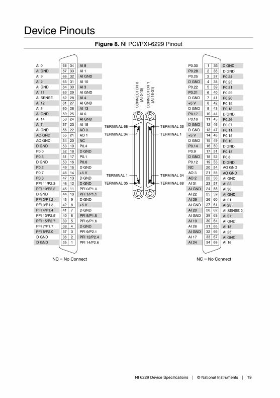
Device PinoutsFigure 8. NI PCI/PXI-6229 Pinout
D GND
D GND
PFI 8/P2.0
PFI 7/P1.7
PFI 15/P2.7
PFI 13/P2.5
PFI 4/P1.4
PFI 3/P1.3
PFI 2/P1.2
D GND
PFI 10/P2.2
PFI 11/P2.3
P0.3
P0.7
P0.2
D GND
P0.5
P0.0
D GND
AO GND
AO GND
AI GND
AI 7
AI 14
AI GND
AI 5
AI 12
AI SENSE
AI 11
AI GND
AI 2
AI 9
AI GND
AI 0
PFI 14/P2.6
PFI 9/P2.1
D GND
PFI 5/P1.5
D GND
+5 V
D GND
PFI 12/P2.4
PFI 6/P1.6
PFI 1/P1.1
PFI 0/P1.0
D GND
D GND
+5 V
D GND
P0.6
P0.1
D GND
P0.4
NC
AO 1
AO 0
AI 15
AI GND
AI 6
AI 13
AI GND
AI 4
AI GND
AI 3
AI 10
AI GND
AI 1
AI 868 34
67 33
66 32
65 31
64 30
63 29
62 28
61 27
60 26
59 25
58 24
57 23
56 22
55 21
54 20
53 19
52 18
51 17
50 16
49 15
48 14
47 13
46 12
45 11
44 10
43 9
42 8
41 7
40 6
39 5
38 4
37 3
36 2
35 1 AI 24
AI 17
AI GND
AI 26
AI 19
AI GND
AI 20
AI GND
AI 29
AI 22
AI GND
AI 31
AO 2
AO 3
NC
P0.12
D GND
P0.9
P0.14
D GND
+5 V
D GND
D GND
P0.16
P0.17
D GND
+5 V
D GND
P0.21
P0.22
D GND
P0.25
P0.28
P0.30
AI 16
AI 25
AI 18
AI 27
AI SENSE 2
AI 28
AI 21
AI GND
AI GND
AI GND
AI 30
AI 23
AI GND
AO GND
AO GNDD GND
P0.8
P0.13
D GND
P0.10
P0.15
P0.11
P0.27
P0.26
D GND
P0.18
P0.19
P0.20
P0.29
P0.31
P0.23
P0.24
D GND
D GND1 35
2 36
3 37
4 38
5 39
6 40
7 41
8 42
9 43
10 44
11 45
12 46
13 47
14 48
15 49
16 50
17 51
18 52
19 53
20 54
21 55
22 56
23 57
24 58
25 59
26 60
27 61
28 62
29 63
30 64
31 65
32 66
33 67
34 68
CO
NN
EC
TOR
0(A
I 0-1
5)
CO
NN
EC
TOR
1(A
I 16-
31)
TERMINAL 34
TERMINAL 68
TERMINAL 35
TERMINAL 1
TERMINAL 35
TERMINAL 1
TERMINAL 34
TERMINAL 68
NC = No Connect NC = No Connect
NI 6229 Device Specifications | © National Instruments | 19
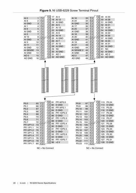
Figure 9. NI USB-6229 Screw Terminal Pinout
17181920212223242526272829303132
AI 4AI 12AI GNDAI 5AI 13AI GNDAI 6AI 14AI GNDAI 7AI 15AI GNDNCAI GNDAO 1AO GND
AI 0AI 8AI GNDAI 1AI 9AI GNDAI 2AI 10AI GNDAI 3AI 11AI GNDAI SENSEAI GNDAO 0AO GND
123456789
10111213141516
49505152535455565758596061626364
AI 20AI 28AI GNDAI 21AI 29AI GNDAI 22AI 30AI GNDAI 23AI 31AI GNDNCAI GNDAO 3AO GND
AI 16AI 24AI GNDAI 17AI 25AI GNDAI 18AI 26AI GNDAI 19AI 27AI GNDAI SENSE 2AI GNDAO 2AO GND
33343536373839404142434445464748
81828384858687888990919293949596
PFI 8/P2.0D GNDPFI 9/P2.1D GNDPFI 10/P2.2D GNDPFI 11/P2.3D GNDPFI 12/P2.4D GNDPFI 13/P2.5D GNDPFI 14/P2.6D GNDPFI 15/P2.7+5 V
P0.0P0.1P0.2P0.3P0.4P0.5P0.6P0.7PFI 0/P1.0PFI 1/P1.1PFI 2/P1.2PFI 3/P1.3PFI 4/P1.4PFI 5/P1.5PFI 6/P1.6PFI 7/P1.7
65666768697071727374757677787980
113114115116117118119120121122123124125126127128
P0.24D GNDP0.25D GNDP0.26D GNDP0.27D GNDP0.28D GNDP0.29D GNDP0.30D GNDP0.31D GND
P0.8P0.9P0.10P0.11P0.12P0.13P0.14P0.15P0.16P0.17P0.18P0.19P0.20P0.21P0.22P0.23
979899
100101102103104105106107108109110111112
NC = No Connect NC = No Connect
20 | ni.com | NI 6229 Device Specifications
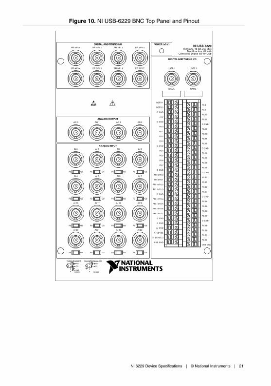
Figure 10. NI USB-6229 BNC Top Panel and Pinout
NI 6229 Device Specifications | © National Instruments | 21

Refer to the NI Trademarks and Logo Guidelines at ni.com/trademarks for information on NI trademarks. Other product andcompany names mentioned herein are trademarks or trade names of their respective companies. For patents covering NIproducts/technology, refer to the appropriate location: Help»Patents in your software, the patents.txt file on your media, or theNational Instruments Patent Notice at ni.com/patents. You can find information about end-user license agreements (EULAs)and third-party legal notices in the readme file for your NI product. Refer to the Export Compliance Information at ni.com/legal/export-compliance for the NI global trade compliance policy and how to obtain relevant HTS codes, ECCNs, and otherimport/export data. NI MAKES NO EXPRESS OR IMPLIED WARRANTIES AS TO THE ACCURACY OF THE INFORMATIONCONTAINED HEREIN AND SHALL NOT BE LIABLE FOR ANY ERRORS. U.S. Government Customers: The data contained inthis manual was developed at private expense and is subject to the applicable limited rights and restricted data rights as set forthin FAR 52.227-14, DFAR 252.227-7014, and DFAR 252.227-7015.
© 2015—2016 National Instruments. All rights reserved.
375204C-01 Jun16