DEVICE SPECIFICATIONS NI PXIe-4339 SPECIFICATIONS NI PXIe-4339 8 Ch, 24-bit, 25.6 kS/s Universal...
23
DEVICE SPECIFICATIONS NI PXIe-4339 8 Ch, 24-bit, 25.6 kS/s Universal Bridge Input Module This document lists specifications for the NI PXIe-4339 universal bridge module. All specifications are subject to change without notice. Visit ni.com/manuals for the most current specifications and product documentation. Note To maintain forced air cooling in the PXIe system, refer to the Maintain Forced-Air Cooling Note to Users. Terminology Maximum and minimum specifications characterize the warranted performance of the instrument within the recommended calibration interval and under the stated operating conditions. These specifications are subject to production verification or guaranteed by design. Typical specifications are specifications met by the majority of the instruments within the recommended calibration interval and under the stated operating conditions, based on measurements taken during production verification and/or engineering development. The performance of the instrument is not warranted. Supplemental specifications describe the basic function and attributes of the instrument established by design and are not subject to production verification. They provide information that is relevant for the adequate use of the instrument that is not included in the previous definitions. All performance specifications are typical unless otherwise noted. These specifications are valid within the full operating temperature range. Accuracy specifications are valid within ±5 °C of the calibration or over the full operating range as specifically noted. Input Characteristics Number of channels .......................................... 8 analog input channels ADC resolution ................................................. 24 bits Type of ADC..................................................... Delta-sigma Sampling mode ................................................. Simultaneous ni.com/manuals Deutsch Français
Transcript of DEVICE SPECIFICATIONS NI PXIe-4339 SPECIFICATIONS NI PXIe-4339 8 Ch, 24-bit, 25.6 kS/s Universal...
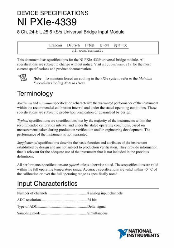
DEVICE SPECIFICATIONS
NI PXIe-43398 Ch, 24-bit, 25.6 kS/s Universal Bridge Input Module
This document lists specifications for the NI PXIe-4339 universal bridge module. All specifications are subject to change without notice. Visit ni.com/manuals for the most current specifications and product documentation.
Note To maintain forced air cooling in the PXIe system, refer to the Maintain Forced-Air Cooling Note to Users.
TerminologyMaximum and minimum specifications characterize the warranted performance of the instrument within the recommended calibration interval and under the stated operating conditions. These specifications are subject to production verification or guaranteed by design.
Typical specifications are specifications met by the majority of the instruments within the recommended calibration interval and under the stated operating conditions, based on measurements taken during production verification and/or engineering development. The performance of the instrument is not warranted.
Supplemental specifications describe the basic function and attributes of the instrument established by design and are not subject to production verification. They provide information that is relevant for the adequate use of the instrument that is not included in the previous definitions.
All performance specifications are typical unless otherwise noted. These specifications are valid within the full operating temperature range. Accuracy specifications are valid within ±5 °C of the calibration or over the full operating range as specifically noted.
Input CharacteristicsNumber of channels.......................................... 8 analog input channels
ADC resolution................................................. 24 bits
Type of ADC..................................................... Delta-sigma
Sampling mode ................................................. Simultaneous
ni.com/manuals
DeutschFrançais

2 | ni.com | NI PXIe-4339 Device Specifications
Voltage mode input ranges................................±100 mV, ±200 mV, ±500 mV, and ±10 V
Ratiometric mode input ranges
Vex ≤ 2.5 V................................................±40 mV/V, ±80 mV/V, ±200 mV/V, and ±4 V/V
Vex ≥ 2.75 V..............................................±10 mV/V, ±20 mV/V, ±50 mV/V, and ±1 V/V
Maximum working voltage(signal + common mode) ..................................±10.5 V for ±10 V, ±1 V/V, and ±4 V/V ranges
±6 V for all other ranges
CMRR (DC to 60 Hz) .......................................72 dB
FIFO buffer size................................................1,023 samples
Data transfers ....................................................Direct memory access (DMA), Programmed I/O
Sample rates (fs)Range ........................................................1 S/s to 25.6 kS/s
Resolution .................................................≤181.9 µS/s
Fault Protection (powered On or Off)
Bridge CompletionHalf-bridge completion
Offset tolerance.........................................±1000 µV/V max, 150 µV/V typ
Stability .....................................................1.25 µV/V per °C max, 0.75 µV/V per °C typ
Quarter-bridge completion................................Surface mount resistor inside the TB-4339 terminal block. Varies by terminal block.Refer to the NI PXIe-4339 and TB-4339/B/C Installation Guide and Terminal Block Specifications for more information.
Signal Level
AI ±<0..7> 30 V between any two pins
RS ±<0..7>
T ±<0..7>
EX ±<0..7>
AO ±<0..7>
SCA <0..7>
PFI0
RSVD 24 V to GND

NI PXIe-4339 Device Specifications | © National Instruments | 3
Shunt CalibrationType .................................................................. Single shunt switch per channel
Resistor ............................................................. Surface mount resistor inside the TB-4339 terminal block. Varies by terminal block. Refer to the NI PXIe-4339 and TB-4339/B/C Installation Guide and Terminal Block Specifications for more information.
Shunt cal switch
Switch resistance ...................................... 10,025 Ω ±0.20% max at 23CStability..................................................... 65 ppm/°C max
Excitation CharacteristicsSelection ........................................................... Software selectable, per channel
Excitation type.................................................. Constant differential voltage (balanced)
Values (Vex)....................................................... 0.625 V, 1 V, 1.5 V, 2 V, 2.5 V,2.75 V, 3.3 V, 5 V, 7.5 V, 10 V
Maximum current ............................................. 30 mA per channel
Maximum fault current ..................................... 38 mA per channel
Maximum Voltage Excitation Settings versus Bridge Configuration
Excitation noise ................................................ 250 µVrms (bandwidth = 11.5 kHz)
Continuous short-circuit protection .................. EX+ to GND,EX- to GND,EX+ to EX-
Bridge Resistance (individual element) Bridge Configuration Vex (max)
120 Ω Full 3.3 V
Half and Quarter 5 V
350 Ω Full 10 V
Half and Quarter
1 kΩ Full
Half and Quarter

4 | ni.com | NI PXIe-4339 Device Specifications
Accuracy1
1 Accuracies listed are warranted for the conditions described in the tables and for up to one year from the module external calibration.
Measurement Conditions
Range: ±100 mV
Gain Error (% of Reading) Offset Error (µV)*
typ (23 °C ±5 °C) 0.02 19
max (23 °C ±5 °C) 0.06 74
max (0 °C to 55 °C) 0.18 133
* Offset error excludes noise. Refer to the Input Noise specifications.
Measurement Conditions
Range: ±200 mV
Gain Error (% of Reading) Offset Error (µV)*
typ (23 °C ±5 °C) 0.02 22
max (23 °C ±5 °C) 0.06 89
max (0 °C to 55 °C) 0.18 165
* Offset error excludes noise. Refer to the Input Noise specifications.
Measurement Conditions
Range: ±500 mV
Gain Error (% of Reading) Offset Error (µV)*
typ (23 °C ±5 °C) 0.02 27
max (23 °C ±5 °C) 0.06 133
max (0 °C to 55 °C) 0.18 252
* Offset error excludes noise. Refer to the Input Noise specifications.
Measurement Conditions
Range: ±10 V
Gain Error (% of Reading) Offset Error (µV)*
typ (23 °C ±5 °C) 0.02 273
max (23 °C ±5 °C) 0.06 1561
max (0 °C to 55 °C) 0.18 3073
* Offset error excludes noise. Refer to the Input Noise specifications.

NI PXIe-4339 Device Specifications | © National Instruments | 5
Measurement Conditions*
Range: ±10 mV/V
Gain Error (% of Reading) Offset Error (µV/V)†
typ (23 °C ±5 °C) 0.02 19/Vex
max (23 °C ±5 °C) 0.1 74/Vex
max (0 °C to 55 °C) 0.2 133/Vex
* Before offset null or shunt calibration, -0.1 V≤ Vcm ≤ 0.1 V. Vcm is the common-mode voltage.† Offset error excludes noise. Refer to the Input Noise specifications.Note: Vex is the excitation voltage. For example: With Vex = 10 V, Offset Error is calculated as19/Vex = 19 µV/10 V = 1.9 µV/V.
Measurement Conditions*
Range: ±20 mV/V
Gain Error (% of Reading) Offset Error (µV/V)†
typ (23 °C ±5 °C) 0.02 22/Vex
max (23 °C ±5 °C) 0.1 89/Vex
max (0 °C to 55 °C) 0.2 165/Vex
* Before offset null or shunt calibration, -0.1 V≤ Vcm ≤ 0.1 V. Vcm is the common-mode voltage.† Offset error excludes noise. Refer to the Input Noise specifications.Note: Vex is the excitation voltage. For example: With Vex = 10 V, Offset Error is calculated as22/Vex = 22 µV/10 V = 2.2 µV/V.
Measurement Conditions*
Range: ±50 mV/V
Gain Error (% of Reading) Offset Error (µV/V)†
typ (23 °C ±5 °C) 0.02 27/Vex
max (23 °C ±5 °C) 0.1 133/Vex
max (0 °C to 55 °C) 0.2 252/Vex
* Before offset null or shunt calibration, -0.1 V≤ Vcm ≤ 0.1 V. Vcm is the common-mode voltage.† Offset error excludes noise. Refer to the Input Noise specifications.Note: Vex is the excitation voltage. For example: With Vex = 10 V, Offset Error is calculated as27/Vex = 27 µV/10 V = 2.7 µV/V.

6 | ni.com | NI PXIe-4339 Device Specifications
Measurement Conditions*
Range: ±1 V/V
Gain Error (% of Reading) Offset Error (µV/V)†
typ (23 °C ±5 °C) 0.02 273/Vex
max (23 °C ±5 °C) 0.1 1561/Vex
max (0 °C to 55 °C) 0.2 2073/Vex
* Before offset null or shunt calibration, -0.1 V≤ Vcm ≤ 0.1 V. Vcm is the common-mode voltage.† Offset error excludes noise. Refer to the Input Noise specifications.Note: Vex is the excitation voltage. For example: With Vex = 10 V, Offset Error is calculated as273/Vex = 273 µV/10 V = 27.3 µV/V.
Measurement Conditions*
Range: ±40 mV/V
Gain Error (% of Reading) Offset Error (µV/V)†
typ (23 °C ±5 °C) 0.02 19/Vex
max (23 °C ±5 °C) 0.1 74/Vex
max (0 °C to 55 °C) 0.2 133/Vex
* Before offset null or shunt calibration, -0.1 V≤ Vcm ≤ 0.1 V. Vcm is the common-mode voltage.† Offset error excludes noise. Refer to the Input Noise specifications.Note: Vex is the excitation voltage. For example: With Vex = 2.5 V, Offset Error is calculated as19/Vex = 19 µV/2.5 V = 7.6 µV/V.
Measurement Conditions*
Range: ±80 mV/V
Gain Error (% of Reading) Offset Error (µV/V)†
typ (23 °C ±5 °C) 0.02 22/Vex
max (23 °C ±5 °C) 0.1 89/Vex
max (0 °C to 55 °C) 0.2 165/Vex
* Before offset null or shunt calibration, -0.1 V≤ Vcm ≤ 0.1 V. Vcm is the common-mode voltage.† Offset error excludes noise. Refer to the Input Noise specifications.Note: Vex is the excitation voltage. For example: With Vex = 2.5 V, Offset Error is calculated as22/Vex = 22 µV/2.5 V = 8.8 µV/V.

NI PXIe-4339 Device Specifications | © National Instruments | 7
Absolute AccuracyAbsolute Accuracy = Reading × Gain Error + Offset Error + Noise Uncertainty,
where Random Noise is the Input noise for the Sample Rate used,3 converts the RMS value to peak value,# samples is the number of samples averaged
If the operating ambient temperature is outside the range of 23 °C ±5 °C, include additional gain error of ΔT × Gain Stability and additional offset error of ΔT × Offset Stability
where ΔT is the temperature difference between the ambient temperature and 18 °C or 28 °C,whichever is smaller.
Measurement Conditions*
Range: ±200 mV/V
Gain Error (% of Reading) Offset Error (µV/V)†
typ (23 °C ±5 °C) 0.02 27/Vex
max (23 °C ±5 °C) 0.1 133/Vex
max (0 °C to 55 °C) 0.2 252/Vex
* Before offset null or shunt calibration, -0.1 V≤ Vcm ≤ 0.1 V. Vcm is the common-mode voltage.† Offset error excludes noise. Refer to the Input Noise specifications.Note: Vex is the excitation voltage. For example: With Vex = 2.5 V, Offset Error is calculated as27/Vex = 27 µV/2.5 V = 10.8 µV/V.
Measurement Conditions*
Range: ±4 V/V
Gain Error (% of Reading) Offset Error (µV/V)†
typ (23 °C ±5 °C) 0.02 273/Vex
max (23 °C ±5 °C) 0.1 1561/Vex
max (0 °C to 55 °C) 0.2 3073/Vex
* Before offset null or shunt calibration, -0.1 V≤ Vcm ≤ 0.1 V. Vcm is the common-mode voltage.† Offset error excludes noise. Refer to the Input Noise specifications.Note: Vex is the excitation voltage. For example: With Vex = 2.5 V, Offset Error is calculated as273/Vex = 273 µV/2.5 V = 109.2 µV/V.
Noise Uncertainty 3Random Noise
# samples-----------------------------------=

8 | ni.com | NI PXIe-4339 Device Specifications
Temperature Stability
Voltage ModeRange: ±100 mV
Gain stability.............................................25 ppm/°C max5 ppm/°C typ
Offset stability...........................................2.2 µV/°C max0.3 µV/°C typ
Range: ±200 mV
Gain stability.............................................25 ppm/°C max5 ppm/°C typ
Offset stability...........................................2.8 µV/°C max0.4 µV/°C typ
Range: ±500 mV
Gain stability.............................................25 ppm/°C max5 ppm/°C typ
Offset stability...........................................4.4 µV/°C max0.64 µV/°C typ
Range: ±10 V
Gain stability.............................................20 ppm/°C max4 ppm/°C typ
Offset stability...........................................56 µV/°C max11.5 µV/°C typ
Ratio ModeRange: ±10 mV/V and ±40 mV/V
Gain stability.............................................25 ppm/°C max5 ppm/°C typ
Offset stability...........................................2.2 µV/Vex per °C max0.3 µV/Vex per °C typ
Range: ±20 mV/V and ±80 mV/V
Gain stability.............................................25 ppm/°C max5 ppm/°C typ
Offset stability...........................................2.8 µV/Vex per °C max0.4 µV/Vex per °C typ
Range: ±50 mV/V and ±200 mV/V
Gain stability.............................................25 ppm/°C max5 ppm/°C typ
Offset stability...........................................4.4 µV/Vex per °C max0.64 µV/Vex per °C typ

NI PXIe-4339 Device Specifications | © National Instruments | 9
Range: ±1 V/V and ±4 V/V
Gain stability............................................. 20 ppm/°C max4 ppm/°C typ
Offset stability .......................................... 56 µV/Vex per °C max11.5 µV/Vex per °C typ
Input NoiseTable 1. Total (µV/Vrms)*, fs = 25.6 kS/s, 350 Ω Full Bridge
Excitation Voltage
Range (±mV/V)
10 20 50 1000 40 80 200 4000
0.625 V — — — — 3.54 3.74 4.66 54.72
1 V — — — — 2.21 2.34 2.91 34.20
1.5 V — — — — 1.47 1.56 1.94 22.80
2 V — — — — 1.11 1.17 1.46 17.10
2.5 V — — — — 0.88 0.94 1.16 13.68
2.75 V 0.80 0.85 1.06 12.44 — — — —
3.3 V 0.67 0.71 0.88 10.36 — — — —
5 V 0.44 0.47 0.58 6.84 — — — —
7.5 V 0.29 0.31 0.39 4.56 — — — —
10 V 0.22 0.23 0.29 3.42 — — — —
* For lower sample rates multiply by , 1 kS/s ≤ fs < 25.6 kS/s.
Table 2. Total (µVrms)*, fs = 25.6 kS/s
Range (±mV)
100 200 500 1000
2.21 2.34 2.91 34.2
* For lower sample rates multiply by , 1 kS/s ≤ fs < 25.6 kS/s.
fs25.6 kS/s----------------------
fs25.6 kS/s----------------------

10 | ni.com | NI PXIe-4339 Device Specifications
Channel-to-channel matching1
Input signal frequency (fin)........................DC to 11.5 kHz
Gain...........................................................0.3%
Phase .........................................................
Phase linearity(fin = DC to 11.5 kHz) .......................................±0.3°
Spurious free dynamic range (SFDR)
1 kHz, -60 dB FS ......................................100 dB
Total harmonic distortion (THD)
1 kHz, -1 dB FS ........................................-88 dB
Filter Group DelayAnalog input delay
1 Identical channel configurations.
Crosstalk (µVrms @ 1 kHz)
Other Channels Operating atFull Scale
Other Channels Operating atHalf Scale
4 2
Input Range Delay (μs)
10 V, 1 V/V, and 4 V/V 6.1
0.5 V, 0.05 V/V, and 0.2 V/V 6.6
0.2 V, 0.02 V/V, and 0.08 V/V 7.1
0.1 V, 0.01 V/V, and 0.04 V/V 7.9
0.035kHz
---------------- fin

NI PXIe-4339 Device Specifications | © National Instruments | 11
Digital filter group delay1, 2 .............................. 1.90976 ms + Variable Filter Delay
Bandwidth and Alias RejectionPassband
Frequency (for 1 S/s ≤ fs < 25 S/s)............ 0.1 × fsFrequency(for 25 S/s ≤ fs ≤ 25.6 kS/s)....................... 0.45 × fsFlatness ..................................................... 0.18 dB for ±100 mV,
±10 mV/V, and ±40 mV/V ranges0.1 dB for all other ranges
1 Digital filter group delay defines the maximum amount of time required after the digitization of a sample begins until the sample is available to be read. The Sample Clock generated by this device for exporting across the PXIe backplane is not affected by the Digital Filter Group Delay.
2 Total digital filter group delay is the total of the fixed portion and the variable delay. For example, the total digital filter group delay for a 10,000 S/s sample rate would be
.
Sample Rate* (fs) Variable Filter Delay (Samples)
1 S/s ≤fs< 25 S/s 3.99
25 S/s ≤fs≤ 47.7 S/s 58.00
47.7 S/s <fs≤ 95.4 S/s 57.99
95.4 S/s <fs≤ 190.7 S/s 57.97
190.7 S/s <fs≤ 381.5 S/s 57.93
381.5 S/s <fs≤ 762.9 S/s 57.86
762.9 S/s <fs≤ 1525.9 S/s 57.71
1525.9 S/s <fs ≤ 3051.8 S/s 57.41
3051.8 S/s <fs≤ 6103.5 S/s 56.82
6103.5 S/s <fs≤ 12207.0 S/s 55.63
12207.0 S/s <fs≤ 24414.1 S/s 53.25
24414.1 S/s <fs≤ 25600 S/s 48.50
* Sample rate range shown is rounded to 0.1 S/s.Precise numbers can be calculated as 100,000,000 ÷ 2n where n is in the range of 12 to 21.For example, the full number for 24414.1 is 100,000,000 ÷ 212 = 24414.0625.
1.90976 ms55.63 S
10,000 S/s-------------------------+ 7.47276 ms=

12 | ni.com | NI PXIe-4339 Device Specifications
Stopband
Frequency (for 1 S/s ≤ fs < 25 S/s)............≥0.9 × fsFrequency(for 25 S/s ≤ fs ≤ 25.6 kS/s).......................≥0.55 × fsRejection ...................................................100 dB
Alias-free bandwidth
(for 1 S/s ≤ fs < 25 S/s)..............................0.1 × fs
Alias-free bandwidth(for 25 S/s ≤ fs ≤ 25.6 kS/s)...............................0.45 × fs
Minimum frequencyfor ADC alias hole ............................................3.125 MHz
Rejection at alias hole .......................................90 dB
Hardware-Timed Single Point Sample ModeAcquisition rate1
Minimum ..................................................1 Hz
Maximum..................................................25.6 kHz
Noise (rms)
±10 V range ..............................................25 Vrms voltage mode
±500 mV range .........................................1.53 Vrms voltage mode
±200 mV range .........................................1.05 Vrms voltage mode
±100 mV range .........................................950 nVrms voltage mode
Hardware-Timed Single Point FilteringFilter type ..........................................................Fourth order, elliptic filter
Stopband attenuation.........................................-120 dB
Passband ripple .................................................0.2 dB
1 Depends on the system setup and application time. Refer to the NI PXIe-4339 User Manual for more information.

NI PXIe-4339 Device Specifications | © National Instruments | 13
Figure 1. Filter Magnitude Response
Figure 2. Passband Ripple
Mag
nitu
de (
dB)
–90
–80
–70
–150
–160–170
–140
–120
–130
–110
–100
–60
–50
0
10
–40
–20
–10
–30
Frequency (Hz)
1M101 100 1k 10k 100k
200 Hz Filter500 Hz Filter1 kHz Filter2 kHz Filter
100 Hz Filter
Mag
nitu
de (
dB)
–0.1
0.075
0.01
0
0.175
–0.075
–0.05
–0.025
0.025
0.05
0.125
0.15
0.275
0.3
0.2
0.25
0.225
Frequency (Hz)
1 10010 10k1k
200 Hz Filter500 Hz Filter1 kHz Filter2 kHz Filter
100 Hz Filter

14 | ni.com | NI PXIe-4339 Device Specifications
Figure 3. Filter Phase Response
Figure 4. Filter Group Delay
Pha
se (
Deg
rees
)
–360
–220
–200
–180
–280
–120
–340
–320
–300
–260
–240
–160
–140
0
–100
–60
–40
–20
–80
Frequency (Hz)
1 k10010 100 k10 k1
200 Hz Filter500 Hz Filter1 kHz Filter2 kHz Filter
100 Hz Filter
Gro
up D
elay
(s)
1 n
10 µ
10 n
100 n
1 µ
100 µ
10 m
1 m
Frequency (Hz)
1 10 k1 k10010 100 k
200 Hz Filter500 Hz Filter1 kHz Filter2 kHz Filter
100 Hz Filter
NI PXIe-4339 Device Specifications | © National Instruments | 15
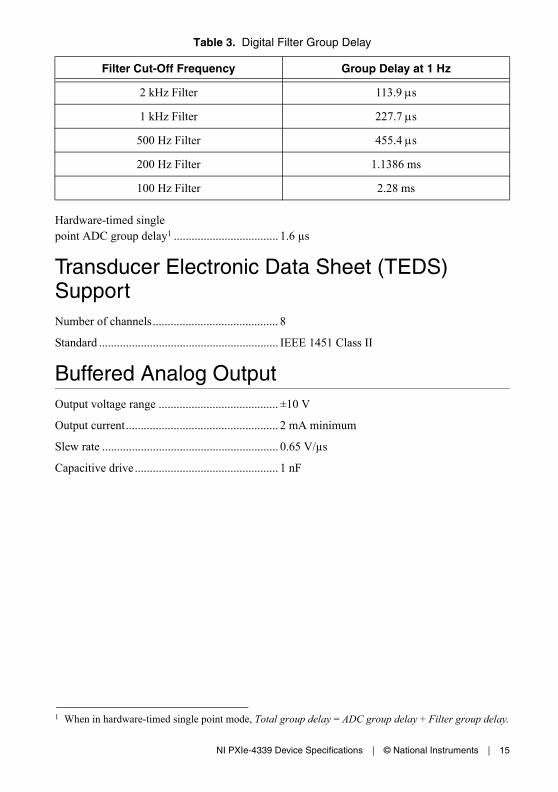
Hardware-timed singlepoint ADC group delay1 ................................... 1.6 µs
Transducer Electronic Data Sheet (TEDS) SupportNumber of channels.......................................... 8
Standard ............................................................ IEEE 1451 Class II
Buffered Analog OutputOutput voltage range ........................................ ±10 V
Output current................................................... 2 mA minimum
Slew rate ........................................................... 0.65 V/µs
Capacitive drive ................................................ 1 nF
Table 3. Digital Filter Group Delay
Filter Cut-Off Frequency Group Delay at 1 Hz
2 kHz Filter 113.9 s
1 kHz Filter 227.7 s
500 Hz Filter 455.4 s
200 Hz Filter 1.1386 ms
100 Hz Filter 2.28 ms
1 When in hardware-timed single point mode, Total group delay = ADC group delay + Filter group delay.

16 | ni.com | NI PXIe-4339 Device Specifications
Output Noise
Gain error ..........................................................0.6% max
Output Offset Error
Internal Frequency Timebase CharacteristicsFrequency..........................................................100 MHz
Accuracy ...........................................................±50 ppm
Front-End Gain(Ranges)
Output Noise(µVrms, Measurement Bandwidth = 10 kHz)
1(±10 V, ±1 V/V, ±4 V/V)
9.5
20(±0.5 V, ±50 mV/V, ±200 mV/V)
48
50(±0.2 V, ±20 mV/V, ±80 mV/V)
112
100(±0.1 V, ±10 mV/V, ±40 mV/V)
220
Front-End Gain (Ranges) Output Offset Error (mV), max
1(±10 V, ±1 V/V, ±4 V/V)
0.6
20(±0.5 V, ±50 mV/V, ±200 mV/V)
5.6
50(±0.2 V, ±20 mV/V, ±80 mV/V)
13.3
100(±0.1 V, ±10 mV/V, ±40 mV/V)
26.4

NI PXIe-4339 Device Specifications | © National Instruments | 17
SynchronizationReference clock source ..................................... Onboard 100 MHz clock, Backplane
PXIe_CLK100
TriggersAnalog trigger
Purpose ..................................................... Reference trigger only
Source ....................................................... AI <0..7>
Level ......................................................... Full scale (depending on input range), programmable
Mode......................................................... Rising-edge, Rising-edge with hysteresis,Falling-edge, Falling-edge with hysteresis, Entering Window, Leaving Window
Resolution................................................. 24 bits
Digital trigger
Purpose ..................................................... Start or reference trigger
Source ....................................................... PFI0, PXI_TRIG<0..7>, PXI_STAR, PXIe_DSTAR<A..B>
Polarity...................................................... Software-selectable
Minimum pulse width............................... 100 ns for PXI_TRIG<0..7>,20 ns for others
Output Timing SignalsSources.............................................................. Sample Clock, Start Trigger Out, Reference
Trigger Out
Destinations ...................................................... PFI0, PXI_TRIG<0..7>, PXIe_DSTARC
Polarity.............................................................. Software-selectable

18 | ni.com | NI PXIe-4339 Device Specifications
PFI CharacteristicsInput
Absolute input voltage range ....................-0.5 V to 6.0 V
Recommended input voltage range...........0 V to 5.5 V
VIH.............................................................2.43 V
VIL .............................................................0.94 V
Input impedance........................................10 kΩ typical, internal pull down resistor
Output
VOH............................................................3 V with IOH = 100 µA2.8 V with IOH = 5 mA
VOL............................................................0.1 V with IOL = -100 µA0.33 V with IOL = -5 mA
Output range .............................................0 V to 3.465 V
Output current ...........................................±5 mA
Output impedance .....................................50 Ω
Bus InterfaceForm factor .......................................................x1 PXI Express peripheral module,
Specification rev 1.0 compliant
Slot compatibility..............................................x1 and x4 PXI Express or PXI Express hybrid slots
DMA channels ..................................................1, analog input
CalibrationYou can obtain the calibration certificate and information about calibration services for the NI PXIe-4339 at ni.com/calibration.
Recommended warm-up time...........................15 minutes
Calibration interval ...........................................1 year

NI PXIe-4339 Device Specifications | © National Instruments | 19
Power Requirements+12 V ................................................................ 1.5 A max
+3.3 V ............................................................... 2.5 A max
Physical RequirementsDimensions ....................................................... Standard 3U PXIe,
16 cm × 10 cm (6.3 in. × 3.9 in.)
Weight............................................................... 186 g (6.6 oz)
I/O connector .................................................... 96-pin male DIN 41612/IEC 60603-2 connector
Caution Clean the hardware with a soft, nonmetallic brush. Make sure that the hardware is completely dry and free from contaminants before returning it to service.
Environmental SpecificationsMaximum altitude............................................. 2,000 m (800 mbar)
Pollution Degree ............................................... 2
Indoor use only.
Operating EnvironmentAmbient temperature range .............................. 0 °C to 55 °C
(Tested in accordance with IEC 60068-2-1 and IEC 60068-2-2. Meets MIL-PRF-28800F Class 3 low temperature limit and MIL-PRF-28800F Class 2 high temperature limit.)
Relative humidity range.................................... 10% to 90%, noncondensing (Tested in accordance with IEC 60068-2-56.)
Storage EnvironmentAmbient temperature range .............................. -40 °C to 71 °C
(Tested in accordance with IEC 60068-2-1 and IEC 60068-2-2. Meets MIL-PRF-28800F Class 3 limits.)
Relative humidity range.................................... 5% to 95%, noncondensing (Tested in accordance with IEC 60068-2-56.)
20 | ni.com | NI PXIe-4339 Device Specifications
Shock and VibrationOperating shock ................................................30 g peak, half-sine, 11 ms pulse
(Tested in accordance with IEC 60068-2-27. Meets MIL-PRF-28800F Class 2 limits.)
Random vibration
Operating ..................................................5 Hz to 500 Hz, 0.3 grms
Non-operating ...........................................5 Hz to 500 Hz, 2.4 grms
(Tested in accordance with IEC 60068-2-64. Non-operating test profile exceeds the requirements of MIL-PRF-28800F, Class 3.)
SafetyThis product meets the requirements of the following standards of safety for electrical equipment for measurement, control, and laboratory use:
• IEC 61010-1, EN 61010-1
• UL 61010-1, CSA 61010-1
Note For UL and other safety certifications, refer to the product label or the Online Product Certification section.
Caution The protection provided by the NI PXIe-4339 can be impaired if it is used in a manner not described in this documents.
Electromagnetic CompatibilityThis product meets the requirements of the following EMC standards for electrical equipment for measurement, control, and laboratory use:
• EN 61326-1 (IEC 61326-1): Class A emissions; Basic immunity
• EN 55011 (CISPR 11): Group 1, Class A emissions
• EN 55022 (CISPR 22): Class A emissions
• EN 55024 (CISPR 24): Immunity
• AS/NZS CISPR 11: Group 1, Class A emissions
• AS/NZS CISPR 22: Class A emissions
• FCC 47 CFR Part 15B: Class A emissions
• ICES-001: Class A emissions
Note In the United States (per FCC 47 CFR), Class A equipment is intended for use in commercial, light-industrial, and heavy-industrial locations. In Europe, Canada, Australia and New Zealand (per CISPR 11) Class A equipment is intended for use only in heavy-industrial locations.

NI PXIe-4339 Device Specifications | © National Instruments | 21
Note Group 1 equipment (per CISPR 11) is any industrial, scientific, or medical equipment that does not intentionally generate radio frequency energy for the treatment of material or inspection/analysis purposes.
Note For EMC declarations and certifications, and additional information, refer to the Online Product Certification section.
CE ComplianceThis product meets the essential requirements of applicable European Directives as follows:
• 2014/35/EU; Low-Voltage Directive (safety)
• 2014/30/EU; Electromagnetic Compatibility Directive (EMC)
Online Product CertificationRefer to the product Declaration of Conformity (DoC) for additional regulatory compliance information. To obtain product certifications and the DoC for this product, visit ni.com/certification, search by model number or product line, and click the appropriate link in the Certification column.
Environmental ManagementNI is committed to designing and manufacturing products in an environmentally responsible manner. NI recognizes that eliminating certain hazardous substances from our products is beneficial to the environment and to NI customers.
For additional environmental information, refer to the Minimize Our Environmental Impact web page at ni.com/environment. This page contains the environmental regulations and directives with which NI complies, as well as other environmental information not included in this document.
Waste Electrical and Electronic Equipment (WEEE)EU Customers At the end of the product life cycle, all products must be sent to a WEEE recycling center. For more information about WEEE recycling centers, National Instruments WEEE initiatives, and compliance with WEEE Directive 2002/96/EC on Waste and Electronic Equipment, visit ni.com/environment/weee.
RoHSNational Instruments
(RoHS) National Instruments RoHS ni.com/environment/rohs_china (For information about China RoHS compliance, go to ni.com/environment/rohs_china.)

22 | ni.com | NI PXIe-4339 Device Specifications
World Wide Support and ServicesThe National Instruments website is your complete resource for technical support. At ni.com/support you have access to everything from troubleshooting and application development self-help resources to email and phone assistance from NI Application Engineers.
Visit ni.com/services for NI Factory Installation Services, repairs, extended warranty, and other services.
Visit ni.com/register to register your National Instruments product. Product registration facilitates technical support and ensures that you receive important information updates from NI.
National Instruments corporate headquarters is located at 11500 North Mopac Expressway, Austin, Texas, 78759-3504. National Instruments also has offices located around the world. For telephone support in the United States, create your service request at ni.com/support or dial 1 866 ASK MYNI (275 6964). For telephone support outside the United States, visit the Worldwide Offices section of ni.com/niglobal to access the branch office websites, which provide up-to-date contact information, support phone numbers, email addresses, and current events.

© 2014–2016 National Instruments. All rights reserved.
376022D-01 May16
Refer to the NI Trademarks and Logo Guidelines at ni.com/trademarks for more information on NI trademarks. Other product and company names mentioned herein are trademarks or trade names of their respective companies. For patents covering NI products/technology, refer to the appropriate location: Help»Patents in your software, the patents.txt file on your media, or the National Instruments Patents Notice at ni.com/patents. You can find information about end-user license agreements (EULAs) and third-party legal notices in the readme file for your NI product. Refer to the Export Compliance Information at ni.com/legal/export-compliance for the NI global trade compliance policy and how to obtain relevant HTS codes, ECCNs, and other import/export data. NI MAKES NO EXPRESS OR IMPLIED WARRANTIES AS TO THE ACCURACY OF THE INFORMATION CONTAINED HEREIN AND SHALL NOT BE LIABLE FOR ANY ERRORS. U.S. Government Customers: The data contained in this manual was developed at private expense and is subject to the applicable limited rights and restricted data rights as set forth in FAR 52.227-14, DFAR 252.227-7014, and DFAR 252.227-7015.