Nanosecond Laser Treatment of a-Si Thin Films for...
8
JLMN-Journal of Laser Micro/Nanoengineering Vol. 12, No. 3, 2017 222 Nanosecond Laser Treatment of a-Si Thin Films for Enhanced Light Trapping and Minority Carrier Lifetime in Photovoltaic Cells Esther Blesso Vidhya Y and Nilesh J Vasa Department of Engineering Design, Indian Institute of Technology, Chennai,600036,India E-mail: [email protected] For thin film solar cells, the efficient collection of light is a challenge, therefore an efficient light-trapping scheme, such as the textures, is required for achieving high light conversion efficien- cies. Laser texturing with a Q-switched, nanosecond pulsed Nd 3+ :YAG laser is used to create nano scale surface roughness in a-Si thin films that enhances light-trapping with simultaneous crystalliza- tion. Changes in surface morphology due to laser assisted texturing in air and water environments on 1-μm thick n-type amorphous silicon film deposited on p-type c-Si is observed using Optical profilometer and Atomic Force Microscopy. The light-trapping properties of textures are analyzed by optical reflectance measurements and compared with theoretical analysis. The extent of crystal- linity and the influence of structural characteristics on electronic properties are studied using I-V characterization and open circuit voltage decay method. Reduction in reflection is observed com- pared to planar surface indicating dependence of reflectance on surface textures which is in agree- ment with the theoretical analysis. After underwater annealing, efficiency of n-aSi/p-cSi solar cells is found to be increased (∼ 2% to 3%) when compared to that in air and diffusion lengths of minori- ty carriers above 1-μm after laser treatment indicates the reduction in the probability of recombina- tion before crossing the junction. Keywords: laser annealing, amorphous silicon, texturing, thin films, solar cells, light trapping, mi- nority carrier life time, diffusion length, finite element method 1. Introduction Crystalline silicon is the most commonly used material for industrial bulk solar-cells due to its efficiency, stability and availability. Thin film solar cells are gaining im- portance because of the reduction in the amount of active material and formation of tandem junctions [1]. Amorphous silicon is a low cost material which is used for electronic devices like thin film transistors [TFTs] and photo voltaic devices. It has high absorption coefficient and the energy gap can be modified to improve the light conversion effi- ciency; tandem junctions can be formed with other ele- ments like carbon and germanium. It can be deposited on a variety of materials at low temperature, over large areas, and on flexible substrates like plastics and polymers [2]. However in amorphous silicon, the absence of crystalline structure and the random network of atoms causes anoma- lous electronic behaviour resulting in low photovoltaic ef- ficiency. Efficiency can be improved by crystallizing the a- Si film by thermal annealing method, such as laser anneal- ing technique [3]. Light trapping is important for thin film solar cells where a single light-pass through the absorber is not suffi- cient to capture the weakly absorbed red and near-infrared photons. The amount of light absorbed depends on the op- tical path length and the absorption coefficient. Textured surface reduces the reflections and increases the optical path length and enhances the optical absorption by light- trapping. This can be achieved by simultaneous formation of laser induced surface texture while annealing [4]. Conventionally, excimer lasers, such as XeCl (308 nm), KrF (248 nm) lasers have been used for annealing of thin film solar cell [5,6]. Due to strong absorption at the surface, they can only be used for the annealing of thin film of few tens of nanometers. Laser-induced crystallization and tex- turing of the film of few hundreds of nm to ≈1000 nm needed for solar applications is a difficult task with excim- er lasers. In addition, they have certain limitations, such as high operational cost and environmental problems due to its toxic nature. Alternatively, Nd 3+ :YAG laser with the fundamental wavelength (1064 nm), the second (532 nm) and the third (355 nm) harmonics can be considered for the treatment of a-Si films [7]. Laser surface texturing of crystalline silicon has been reported [8,9], however, there are limited work on simulta- neous annealing and texturing of a-Si thin films in air and water[10]. Most of the studies reported use femtosecond lasers, which involve ablation induced surface structuring. Simultaneous wide-area annealing and texturing of thick (> few hundred nm) a-Si films in air and water ambience us- ing laser-assisted melting and re-solidification approach without ablation is a challenging task. This approach in- duces the texture formation via capillary action in molten silicon without ablating the material [4]. In our earlier works, we reported the effect of laser flu- ence, beam profile, laser wavelength and ambience on the surface morphology of the thin film and the extent of crys- tallinity with various characterization techniques [11,12]. In this paper, the formation of light trapping structures and DOI: 10.2961/jlmn.2017.03.0009
Transcript of Nanosecond Laser Treatment of a-Si Thin Films for...
JLMN-Journal of Laser Micro/Nanoengineering Vol. 12, No. 3, 2017
222
Nanosecond Laser Treatment of a-Si Thin Films for Enhanced Light Trapping and Minority Carrier Lifetime in Photovoltaic Cells
Esther Blesso Vidhya Y and Nilesh J Vasa
Department of Engineering Design, Indian Institute of Technology, Chennai,600036,India
E-mail: [email protected]
For thin film solar cells, the efficient collection of light is a challenge, therefore an efficient light-trapping scheme, such as the textures, is required for achieving high light conversion efficien-cies. Laser texturing with a Q-switched, nanosecond pulsed Nd3+:YAG laser is used to create nano scale surface roughness in a-Si thin films that enhances light-trapping with simultaneous crystalliza-tion. Changes in surface morphology due to laser assisted texturing in air and water environments on 1-μm thick n-type amorphous silicon film deposited on p-type c-Si is observed using Optical profilometer and Atomic Force Microscopy. The light-trapping properties of textures are analyzed by optical reflectance measurements and compared with theoretical analysis. The extent of crystal-linity and the influence of structural characteristics on electronic properties are studied using I-V characterization and open circuit voltage decay method. Reduction in reflection is observed com-pared to planar surface indicating dependence of reflectance on surface textures which is in agree-ment with the theoretical analysis. After underwater annealing, efficiency of n-aSi/p-cSi solar cells is found to be increased (∼ 2% to 3%) when compared to that in air and diffusion lengths of minori-ty carriers above 1-μm after laser treatment indicates the reduction in the probability of recombina-tion before crossing the junction.
Keywords: laser annealing, amorphous silicon, texturing, thin films, solar cells, light trapping, mi-nority carrier life time, diffusion length, finite element method
1. Introduction Crystalline silicon is the most commonly used material
for industrial bulk solar-cells due to its efficiency, stability and availability. Thin film solar cells are gaining im-portance because of the reduction in the amount of active material and formation of tandem junctions [1]. Amorphous silicon is a low cost material which is used for electronic devices like thin film transistors [TFTs] and photo voltaic devices. It has high absorption coefficient and the energy gap can be modified to improve the light conversion effi-ciency; tandem junctions can be formed with other ele-ments like carbon and germanium. It can be deposited on a variety of materials at low temperature, over large areas, and on flexible substrates like plastics and polymers [2]. However in amorphous silicon, the absence of crystalline structure and the random network of atoms causes anoma-lous electronic behaviour resulting in low photovoltaic ef-ficiency. Efficiency can be improved by crystallizing the a-Si film by thermal annealing method, such as laser anneal-ing technique [3].
Light trapping is important for thin film solar cells where a single light-pass through the absorber is not suffi-cient to capture the weakly absorbed red and near-infrared photons. The amount of light absorbed depends on the op-tical path length and the absorption coefficient. Textured surface reduces the reflections and increases the optical path length and enhances the optical absorption by light-trapping. This can be achieved by simultaneous formation of laser induced surface texture while annealing [4].
Conventionally, excimer lasers, such as XeCl (308 nm), KrF (248 nm) lasers have been used for annealing of thin film solar cell [5,6]. Due to strong absorption at the surface, they can only be used for the annealing of thin film of few tens of nanometers. Laser-induced crystallization and tex-turing of the film of few hundreds of nm to ≈1000 nm needed for solar applications is a difficult task with excim-er lasers. In addition, they have certain limitations, such as high operational cost and environmental problems due to its toxic nature. Alternatively, Nd3+:YAG laser with the fundamental wavelength (1064 nm), the second (532 nm) and the third (355 nm) harmonics can be considered for the treatment of a-Si films [7].
Laser surface texturing of crystalline silicon has been reported [8,9], however, there are limited work on simulta-neous annealing and texturing of a-Si thin films in air and water[10]. Most of the studies reported use femtosecond lasers, which involve ablation induced surface structuring. Simultaneous wide-area annealing and texturing of thick (> few hundred nm) a-Si films in air and water ambience us-ing laser-assisted melting and re-solidification approach without ablation is a challenging task. This approach in-duces the texture formation via capillary action in molten silicon without ablating the material [4].
In our earlier works, we reported the effect of laser flu-ence, beam profile, laser wavelength and ambience on the surface morphology of the thin film and the extent of crys-tallinity with various characterization techniques [11,12]. In this paper, the formation of light trapping structures and
DOI: 10.2961/jlmn.2017.03.0009

JLMN-Journal of Laser Micro/Nanoengineering Vol. 12, No. 3, 2017
223
crystallization characteristics of a-Si thin film annealed and textured using the solid-state Nd3+:YAG laser in air and water environment is studied. The dependence of properties like reflectance, transmittance and absorptance on surface textures are analyzed by numerical simulations based on Maxwell’s wave equations with periodic surface textures with different dimensions and density. The extent of crys-tallinity and the influence of structural characteristics on electronic properties are studied using I-V characterization and the calculation of minority carrier life time and diffu-sion length using the open circuit voltage decay method.
2. Experiment Experiments are performed in different ambience such
as in air and water to determine appropriate conditions for annealing and texturing of a-Si films. P-type (Boron doped) crystalline silicon wafers of 275 ± 25 µm thick-ness coated with n-type (Phosphorous doped) amorphous silicon films of 0.4 µm and 1 µm thickness by plasma-enhanced chemical vapor deposition technique (Hind High Vacuum Co., India) using silane (SiH4), Hydrogen and 1% phosphine in silane at 1 torr pressure and 40 mW/cm2 pow-er density are used in these experiments.
Figure 1 shows the schematic of the experimental setup. Laser annealing is performed using a solid-state, pulsed Nd3+:YAG laser (Brilliant b, Quantel) with a wavelength of 532 nm and 355 nm, pulse duration of 5 ns (FWHM) and pulse repetition rate of 1 Hz. A plano-convex Lens with a focal length of 200 mm is used to form a 2 mm laser spot size on a-Si film. Distance between the lens and sample was adjusted to obtain the same laser spot size in air and water. The laser beam with a Gaussian and a flat-top beam profile were used in the experiments. The Gaussian beam profile was changed into the flat-top beam profile using a dispersion based beam shaper (π Shaper 12_12_532_HP, AdlOptica). To determine the fluence range for laser melt-ing, surface reflectivity measurements are performed with a red diode laser (635 nm) as a probe laser as reported in our earlier work[4]. For under water experiments samples are kept at 3 mm depth in the deionized water. 10 mm × 10 mm samples are scanned with laser spot overlapping for simultaneous crystallization and texturization of wide area a-Si, with 30%, 50% and 90% of the spot diameter as an overlap as shown in figure 1(b).
The formation light trapping textures are studied by a
scanning electron microscope (SEM), optical profilometry (Bruker, 3D Non-contact Profiler, Contour GT-I) and the
Fig. 1 (a) Experimental setup for nanosecond Laser annealing (b) Laser spot overlap.
Fig. 2 Surface Profile of a-Si/c-Si sample showing regions of untreated and treated with ns-laser at 532 nm with 150 mJ/cm2 (a),(b) 2D image and its roughness profile (c) 3D profile (The left region in each image is untreated region).

JLMN-Journal of Laser Micro/Nanoengineering Vol. 12, No. 3, 2017
224
atomic force microscopy (AFM) (Bruker, Dimension edge) to analyze the texturing effect. The effect of light trapping textures on optical reflectance is analyzed using a broad-band light source and a monochromator system (Bentham PVE 300). The effect of crystallization on the electronic properties are studied using I-V characterization and the open circuit voltage decay method using a white light Xe lamp and an AM 1.5 filter with a digital storage oscillo-scope (Lecroy, wave runner, 250 MHz) and electrical source/ measurement unit (B2901A, Keysight).
3. Theoretical analysis
In this numerical analysis, geometrical structures are theoretically investigated on a nanometer scale to improve the optical properties of the textured surface of Si solar cells. Maxwell's equations, are solved to model the optical properties of surfaces that have been textured. This em-ploys full wave finite element method to simulate the inter-action of the incident light with nanostructure, which is realized by infinitely extending the unit texture using peri-odic boundary conditions. Then the electromagnetic field distribution can be obtained through resolving Maxwell’s equations. Thereby, the spatial distribution of the energy flux, and thus the optical characteristics such as reflection, transmission, and absorption spectra, can be obtained by integrating the calculated electromagnetic field [13].
The simulations are carried out using the RF module of COMSOL 5.2 Multiphysics software package. The optical properties of materials are described by complex wave-length-dependent refraction index. The simulation is car-ried out for TE polarized wave and at wavelengths in the range of absorption of Si (300 nm to 1100 nm). 2-D peri-odic textures are considered in the simulations. The di-mensions of the texture period and height have been varied based on the experimental observations.
4. Results and discussions
4.1 Light trapping Laser-assisted melting and resolidification approach in-
duces the texture formation via capillary action in molten silicon without ablating the material. As the laser interacts with the material surface, the temperature rises with possi-ble phase changes. Due to the surface tension, capillary waves are generated. The capillary waves will exist in the liquefied region until silicon starts cooling due to thermal conductivity and the waves are frozen to change the surface topology. These structures subsequently sharpen into spikes by repeated overlapping of pulses.
Figure 2 shows the surface characteristics of laser treat-ed a-Si films, by using the optical profilometer. Fig. 2(a) and (c) shows the 2D and 3D surface roughness profile of the sample and (b) shows the surface profile along red line in Fig. 2(a) (X-direction). Left region of in Figs. 2(a) and (b) show the untreated region where the surface is smooth and the treated region on the right clearly indicates the formation of textures after laser treatment. Based on the optical profilometer studies, in the case of the Gaussian beam annealing at the laser fluence of 150 mJ/cm2 in air, an average height of 300 nm texture formation is observed.
Figures 3(a), (b) and (c) show AFM images of the laser textured a-Si film samples with 30%, 50% and 90% of beam overlap corresponding to the Gaussian beam profile in air with 355 nm wavelength, respectively. The density and uniformity of texture peaks are increased with the flat-top beam profile and water ambience [4]. Root mean square (RMS) value of surface roughness (Rq parameter) is estimated from AFM images. Figure 3(d) shows variation of surface roughness (Rq) values of the samples shown in Figs. 3(a) to (c) compared with the samples treated with flat-top beam profiles. The increase in surface roughness is
Fig. 3 AFM images of laser treated a-Si/c-Si with Gaussian beam profile in air and (a) 30% (b) 50% and (c) 90% of laser spot overap and (d) RMS roughness with Gaussian and flat-top beams with a fluence of 300mJ/ cm2.
JLMN-Journal of Laser Micro/Nanoengineering Vol. 12, No. 3, 2017
225
observed for the increase in laser spot overlap. From the comparative investigation with 50% and 90% overlap for a-Si/c-Si samples, it is observed that, the samples with 90% overlap and treated in air show higher Rq values. In the case of flat-top beam profile with a lower percentage of overlap, the textures are almost uniform and the surface roughness variation is negligible throughout the film sur-face whereas with Gaussian beam profile significant sur-face roughness variation is observed. As percentage of overlap increased, the uniformity of textures with Gaussi-an beam profiles also increased.
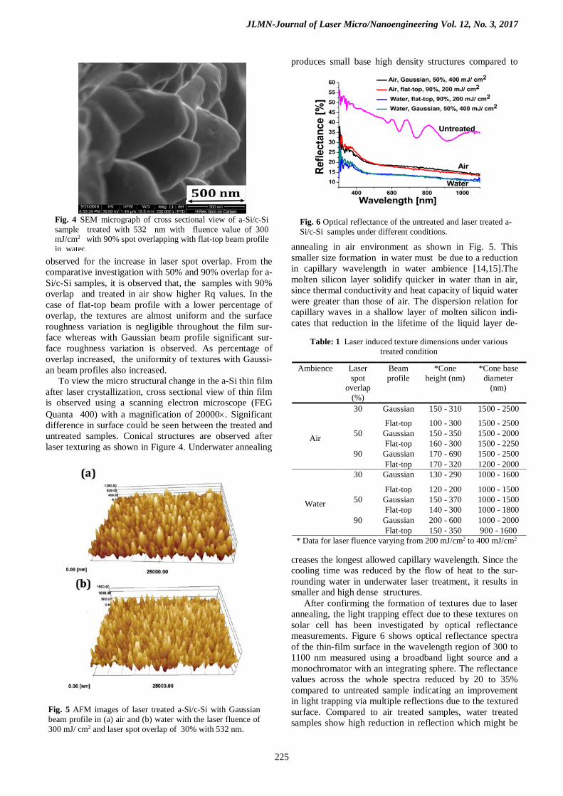
To view the micro structural change in the a-Si thin film after laser crystallization, cross sectional view of thin film is observed using a scanning electron microscope (FEG Quanta 400) with a magnification of 20000×. Significant difference in surface could be seen between the treated and untreated samples. Conical structures are observed after laser texturing as shown in Figure 4. Underwater annealing
produces small base high density structures compared to
annealing in air environment as shown in Fig. 5. This smaller size formation in water must be due to a reduction in capillary wavelength in water ambience [14,15].The molten silicon layer solidify quicker in water than in air, since thermal conductivity and heat capacity of liquid water were greater than those of air. The dispersion relation for capillary waves in a shallow layer of molten silicon indi-cates that reduction in the lifetime of the liquid layer de-
creases the longest allowed capillary wavelength. Since the cooling time was reduced by the flow of heat to the sur-rounding water in underwater laser treatment, it results in smaller and high dense structures.
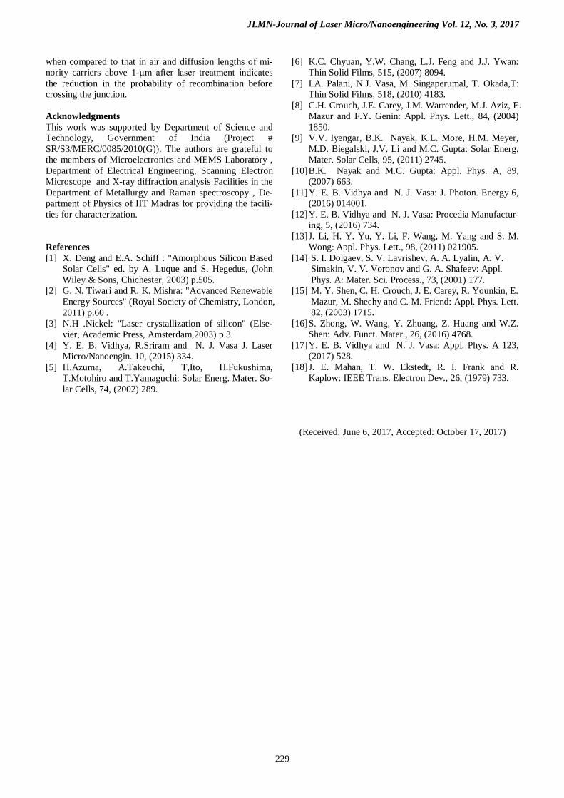
After confirming the formation of textures due to laser annealing, the light trapping effect due to these textures on solar cell has been investigated by optical reflectance measurements. Figure 6 shows optical reflectance spectra of the thin-film surface in the wavelength region of 300 to 1100 nm measured using a broadband light source and a monochromator with an integrating sphere. The reflectance values across the whole spectra reduced by 20 to 35% compared to untreated sample indicating an improvement in light trapping via multiple reflections due to the textured surface. Compared to air treated samples, water treated samples show high reduction in reflection which might be
Fig. 4 SEM micrograph of cross sectional view of a-Si/c-Si sample treated with 532 nm with fluence value of 300 mJ/cm2 with 90% spot overlapping with flat-top beam profile in water.
Fig. 6 Optical reflectance of the untreated and laser treated a-Si/c-Si samples under different conditions.
Table: 1 Laser induced texture dimensions under various treated condition
Ambience Laser spot
overlap (%)
Beam profile
*Cone height (nm)
*Cone base diameter
(nm)
Air
30 Gaussian 150 - 310 1500 - 2500
Flat-top 100 - 300 1500 - 2500 50 Gaussian 150 - 350 1500 - 2000
Flat-top 160 - 300 1500 - 2250 90 Gaussian 170 - 690 1500 - 2500
Flat-top 170 - 320 1200 - 2000
Water
30 Gaussian 130 - 290 1000 - 1600
Flat-top 120 - 200 1000 - 1500 50 Gaussian 150 - 370 1000 - 1500
Flat-top 140 - 300 1000 - 1800 90 Gaussian 200 - 600 1000 - 2000
Flat-top 150 - 350 900 - 1600 * Data for laser fluence varying from 200 mJ/cm2 to 400 mJ/cm2
Fig. 5 AFM images of laser treated a-Si/c-Si with Gaussian beam profile in (a) air and (b) water with the laser fluence of 300 mJ/ cm2 and laser spot overlap of 30% with 532 nm.

JLMN-Journal of Laser Micro/Nanoengineering Vol. 12, No. 3, 2017
226
due to the high dense textures and large crystal grains found in water treated samples [11].
Additionally, the experimental result is compared with simulation as shown in Fig. 7. For the numerical simulation, finite element method is used to solve the Maxwell’s equa-tion to model the laser induced structure. From AFM anal-
ysis, the experimentally formed conical textures base dim-eters are found to be ~1500 to 2500 nm for air and ~1000 to 2000 nm in water and the height values are in between 100 nm and 700 nm for both air and water. The average texture dimensions derived from AFM analysis are listed in Table 1. The texture height values 200 nm and 500 nm and base diameter 2000 nm which are in these range are chosen for the analysis. The conical textures formed with laser texturing are slightly randomized and has small order of multi scale structures, because of the slight variation of fluences and temperatures during the experimental process. In this study, since the exact random structure produced by laser texturing is difficult to reproduce or realize via simu-lation method, dimensions approaching the average size of the cone based on the experimental study are considered.
An unit cone bounded by periodical condition is irradi-ated with sunlight of wavelength ranging from 300 nm to 1100 nm. The height and density of the cones are varied and angular and wavelength dependence of absorption and reflection are calculated. Figure 7(a) and (b) show the re-flection and absorption spectra for the structure under anal-ysis with normal incidence of light. The 1000 nm thick untextured plane surface serves as the reference. It is clear that light reflection decreases after incorporating the sur-face texturing, and the antireflection becomes more effec-tive with increasing the height and absorption in the longer wavelength also increases. When the texture height in-creases from 200 to 500 nm, the top angle of the conical texture decreases, increasing the number of multiple reflec-tions, thus increasing the optical path length. Also, the longer wavelength of the incident light wave can easily penetrate through the small textures whereas taller textures produce reflections which enhances absorption. Silicon has week absorption at longer wavelength and this is the indi-
Fig. 7 Spectral (a) absorptance (b) reflectance with normal incidence of light and (c) absorptance (d) reflectance as a function of light incident angle for the wave length 400 nm. The results are shown for flat cell, and two textured cells with different texture size. The inset figure in (c) shows texture dimensions used in these analysis.
Fig. 8 Spectral (a) absorptance (b) reflectance as a function of different density for the texture height of 700 nm and base di-ameter of 1500 nm. The inset figure in (a) shows texture di-mensions used in these analysis.

JLMN-Journal of Laser Micro/Nanoengineering Vol. 12, No. 3, 2017
227
cation that the increased optical path length with increased height allows for the silicon to absorb weekly absorbed photons with longer wavelength. Further analysis with in-creasing height has shown that after around 300 to 400 nm height, the integrated values of absorption and reflection over the silicon absorption spectrum of 300 nm to 1100 nm becomes almost constant, and the change in base diameter has little effect on these properties. These analysis clearly shows that by creating a texture of height 600 nm with la-ser texturing, we can achieve optimum efficiency. Figures 7(c) and (d) show lower incidence angles starting from normal incidence of light on the solar cell plane gives high-er absorption and minimizes the reflection compared to other higher angular incidence.
The influence of texture density on absorptance and re-flectance characteristics are studied by varying the perio-dicity of the textures. Figures 8(a) and (b) show spectral absorptance and reflectance as a function of different den-sity for the texture height of 700 nm and base diameter of 1500 nm. The density is changed by varying the peak to peak distance from 1875 nm to 3750 nm. From the Figs. 8(a) and (b) it is clearly seen that absorption enhancement and reduction in reflection is more in high density textures compared to lower density textures, due to the increased scattering in high density structures. Recent studies on the random Si nanopyramids fabricated by etching process showed an improvement in light trapping efficiency in ultrathin c-Si (few tens of micrometers) [16]. Further anal-ysis is essential to simulate light trapping and influence of wavelength in random structures.
4.2 Open circuit voltage decay measurements The defects and dangling bonds in a-Si/poly-Si materi-
als can cause a decrease in the carrier lifetime, which may in turn reduce the carrier diffusion length. This leads to reduction in the overall energy conversion efficiency. Car-rier lifetime can be improved by annealing the a-Si and
when it is performed in water, due to very high laser in-duced temperature water molecules break in to hydrogen, oxygen and hydroxyl radicals [17]. This atomic hydrogen penetrates the film during annealing and attaches itself to defects and deactivate them. The open circuit voltage decay method is used for measuring the minority carrier lifetime [18]. The open-circuit voltage is measured as a function of time at the end of the light pulse, and by analysing the de-cay curve, the minority carrier lifetime can be calculated as shown in Fig. 9. AM 1.5 filtered Xe-lamp provided the light, cut down by light chopper (frequency 4000 Hz) and the voltage-decay signal is captured using a 250 MHz Digi-tal storage Oscilloscope (Lecroy, wave runner). The exper-imental set-up is shown in Fig. 9(a).
The decay curve contains three regions of interest, high, intermediate and low levels of injection as reported in [14]. In the first two regions, the decay curve is linear whereas in the low level of injection, it becomes exponential as shown in figure 10 (a). The life time of minority carriers can be calculated with the slope of each region using the following equations:
2𝐾𝐾𝐾𝐾𝑞𝑞
[ 𝑑𝑑𝑑𝑑𝑑𝑑𝑑𝑑𝑑𝑑𝑑𝑑
] - Region 1 (1)
𝐾𝐾𝐾𝐾𝑞𝑞
[ 𝑑𝑑𝑑𝑑𝑑𝑑𝑑𝑑𝑑𝑑𝑑𝑑
] - Region 2 (2)
𝐾𝐾𝐾𝐾𝑞𝑞
[𝑒𝑒𝑒𝑒𝑒𝑒[ 𝑞𝑞𝑑𝑑(0)𝐾𝐾𝐾𝐾
− 1] 𝑒𝑒𝑒𝑒𝑒𝑒(−𝑑𝑑𝜏𝜏
) - Region 3 (3) where the lifetime of the minority carrier is τ, K is
Boltzmann’s constant, T is the absolute temperature, q is the electron charge, t is the time and 𝑑𝑑𝑑𝑑𝑑𝑑𝑑𝑑 𝑑𝑑𝑑𝑑 is the slope of in each region and V(0) is the open circuit voltage at the termination of excitation. Here we used intermediate region for the calculation of minority carrier life time and from which diffusion length is calculated as follows.
Diffusion length: 𝐿𝐿 = √𝐷𝐷𝐷𝐷 (4) Diffusivity : 𝐷𝐷 = 𝜇𝜇 𝐾𝐾𝐾𝐾𝑞𝑞 (5) where μ is the mobility of the minority carriers and the
calculated minority carrier life times are shown in table 1. Water annealed sample shows 13% improvement in the lifetime of minority carriers compared to air treated sam-ples which indicates defects passivation with hydrogen in water.
Minority carrier diffusion length is important since it determine whether the carrier can cross the junction before recombination. Since our samples are n-type a-Si, minority hole mobility is considered. As per literature, it can vary from 0.01 cm2/V-S to several hundred cm2/V-S depending
Fig. 9 (a) Experimental setup for open circuit voltage decay measurements (b) Open circuit voltage decay curve.
Table 2 Minority carrier lifetime with the laser fluence 300 mJ /cm2 with different spot overlap
Ambience 30 90
a i r 30 μs 22 .3 μs wat er 33 .45 μs 25 .1 μs

JLMN-Journal of Laser Micro/Nanoengineering Vol. 12, No. 3, 2017
228
on the concentration. By considering these values, diffu-sion lengths for the calculated minority carriers are pre-sented in Fig. 9(b). Even for the least possible value of 0.01 cm2/V-S, which is in a-Si range, the diffusion length is around 900 nm and for poly-Si it is above 30 μm which is sufficient for the carriers to cross the junction which is 1μm away from surface for our experimental samples.
4.3 I-V characteristics
Light I-V characteristics measurements are done by il-luminating the sample using a Xe light source measuring the current and voltage with the precision source/ Meas-urement unit (B2901A, Keysight). The input intensity of the light at the sample surface is set to 60 mW/cm2 . The efficiency of the untreated a-Si sample is found to be around 0.013% . After laser treatment, efficiency improves depending on the experimental conditions. Figures 11(a) and (b) show current - voltage measurements of laser treat-ed samples in air and water for 50% of spot overlapping and the corresponding calculated values of efficiency for different percentage of spot overlap. Even though 90% overlapped samples gives better light trapping textures with high roughness values, efficiencies of 30% and 50% are found to be as compared to that of 90% overlapping. This might be due to the removal of material and higher order of defects and damage inflicted on the sample due repeated irradiation of laser pulse on the same spot when treated with higher percentage of overlapping. The ablation threshold might have decreased with increasing number of pulses due to change in the nature and absorption behavior
of the film after each laser pulse irradiation. Overall, there is a significant improvement in the absorption of incident light due to textured surface. Underwater treated samples gives better I-V values compared to that of air treatment. These improved electrical characteristics in underwater annealing is an indication of high density light trapping structures and better crystallization.
5. Conclusions
Laser annealing and texturing with a Q-switched, na-nosecond pulsed Nd3+:YAG laser is performed and the formation of nano scale surface roughness in a-Si thin films that strongly enhances light-trapping with simultane-ous crystallization is studied. Changes in surface morphol-ogy due to laser assisted texturing in air and water envi-ronments is observed using Optical profilometer, Scanning electron microscope and Atomic Force Microscopy. The light-trapping properties of textures are analyzed by optical reflectance measurements and compared with theoretical analysis. Theoretical analysis is performed by solving maxwell's equation and the incident angle and wavelength dependance of reflectance and absorptance is studied. Re-duction in reflection is observed compared to planar sur-face indicating dependence of reflectance on surface tex-tures which is in agreement with the theoretical analysis. The extent of crystallinity and the influence of structural characteristics on electronic properties are studied using I-V characterization and the open circuit voltage decay method. After underwater annealing, the efficiency of n-aSi/p-cSi solar cells is found to be increased (∼ 2 to 3%)
Fig. 11 (a) Current–voltage curve under illumination of the laser treated sample in air and water with 50% spot overlap and (b) efficiency for different percentage of spot overlap for 532 nm and fluence 300 mJ/cm2.
Fig. 10 (a) Open circuit voltage decay curve with three re-gions of interest (d) Diffusion length of minority carriers of the laser treated sample in air and water for 532 nm with 300 mJ/cm2.
JLMN-Journal of Laser Micro/Nanoengineering Vol. 12, No. 3, 2017
229
when compared to that in air and diffusion lengths of mi-nority carriers above 1-μm after laser treatment indicates the reduction in the probability of recombination before crossing the junction.
Acknowledgments This work was supported by Department of Science and Technology, Government of India (Project # SR/S3/MERC/0085/2010(G)). The authors are grateful to the members of Microelectronics and MEMS Laboratory , Department of Electrical Engineering, Scanning Electron Microscope and X-ray diffraction analysis Facilities in the Department of Metallurgy and Raman spectroscopy , De-partment of Physics of IIT Madras for providing the facili-ties for characterization. References [1] X. Deng and E.A. Schiff : "Amorphous Silicon Based
Solar Cells" ed. by A. Luque and S. Hegedus, (John Wiley & Sons, Chichester, 2003) p.505.
[2] G. N. Tiwari and R. K. Mishra: "Advanced Renewable Energy Sources" (Royal Society of Chemistry, London, 2011) p.60 .
[3] N.H .Nickel: "Laser crystallization of silicon" (Else-vier, Academic Press, Amsterdam,2003) p.3.
[4] Y. E. B. Vidhya, R.Sriram and N. J. Vasa J. Laser Micro/Nanoengin. 10, (2015) 334.
[5] H.Azuma, A.Takeuchi, T,Ito, H.Fukushima, T.Motohiro and T.Yamaguchi: Solar Energ. Mater. So-lar Cells, 74, (2002) 289.
[6] K.C. Chyuan, Y.W. Chang, L.J. Feng and J.J. Ywan: Thin Solid Films, 515, (2007) 8094.
[7] I.A. Palani, N.J. Vasa, M. Singaperumal, T. Okada,T: Thin Solid Films, 518, (2010) 4183.
[8] C.H. Crouch, J.E. Carey, J.M. Warrender, M.J. Aziz, E. Mazur and F.Y. Genin: Appl. Phys. Lett., 84, (2004) 1850.
[9] V.V. Iyengar, B.K. Nayak, K.L. More, H.M. Meyer, M.D. Biegalski, J.V. Li and M.C. Gupta: Solar Energ. Mater. Solar Cells, 95, (2011) 2745.
[10] B.K. Nayak and M.C. Gupta: Appl. Phys. A, 89, (2007) 663.
[11] Y. E. B. Vidhya and N. J. Vasa: J. Photon. Energy 6, (2016) 014001.
[12] Y. E. B. Vidhya and N. J. Vasa: Procedia Manufactur-ing, 5, (2016) 734.
[13] J. Li, H. Y. Yu, Y. Li, F. Wang, M. Yang and S. M. Wong: Appl. Phys. Lett., 98, (2011) 021905.
[14] S. I. Dolgaev, S. V. Lavrishev, A. A. Lyalin, A. V. Simakin, V. V. Voronov and G. A. Shafeev: Appl. Phys. A: Mater. Sci. Process., 73, (2001) 177.
[15] M. Y. Shen, C. H. Crouch, J. E. Carey, R. Younkin, E. Mazur, M. Sheehy and C. M. Friend: Appl. Phys. Lett. 82, (2003) 1715.
[16] S. Zhong, W. Wang, Y. Zhuang, Z. Huang and W.Z. Shen: Adv. Funct. Mater., 26, (2016) 4768.
[17] Y. E. B. Vidhya and N. J. Vasa: Appl. Phys. A 123, (2017) 528.
[18] J. E. Mahan, T. W. Ekstedt, R. I. Frank and R. Kaplow: IEEE Trans. Electron Dev., 26, (1979) 733.
(Received: June 6, 2017, Accepted: October 17, 2017)
http://profiles.spiedigitallibrary.org/summary.aspx?DOI=10.1117%2f1.JPE.6.014001&Name=Nilesh+J.+Vasa
http://profiles.spiedigitallibrary.org/summary.aspx?DOI=10.1117%2f1.JPE.6.014001&Name=Nilesh+J.+Vasa