Laser Direct Write - jlps.gr.jpjlps.gr.jp/jlmn/upload/52b472dad76c3b4651765094547f4dd6.pdf · Laser...
8
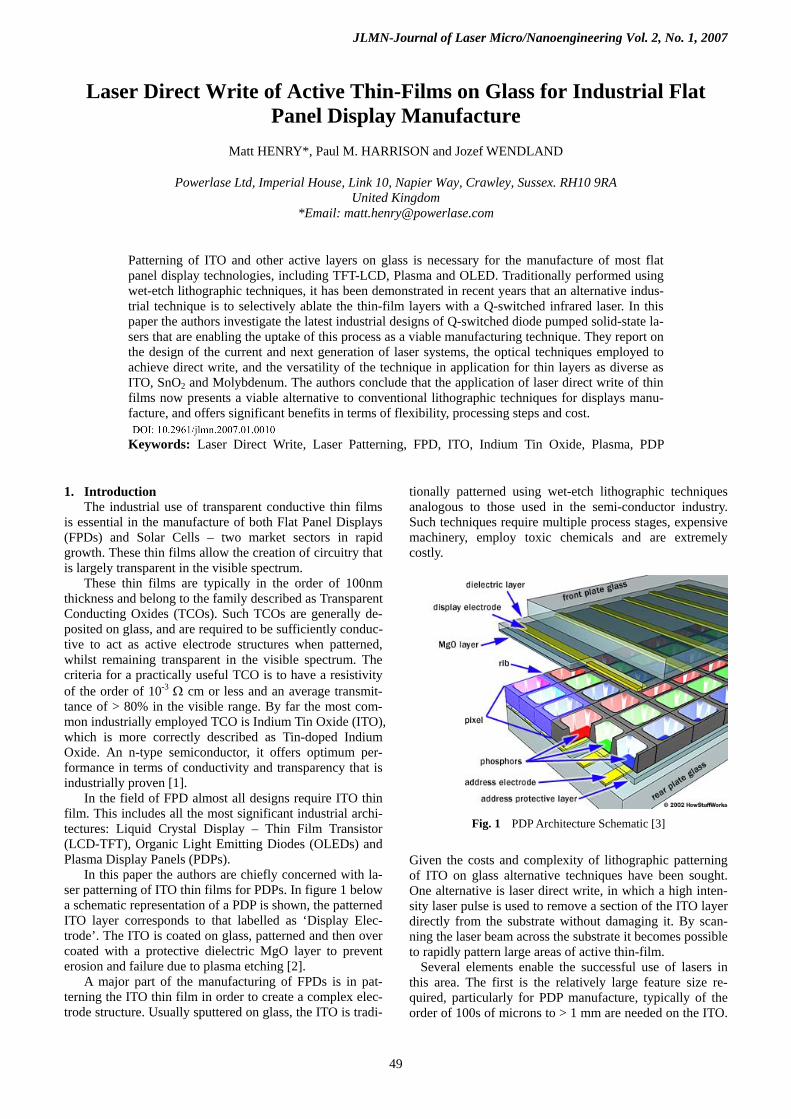
JLMN-Journal of Laser Micro/Nanoengineering Vol. 2, No. 1, 2007 Laser Direct Write of Active Thin-Films on Glass for Industrial Flat Panel Display Manufacture Matt HENRY*, Paul M. HARRISON and Jozef WENDLAND Powerlase Ltd, Imperial House, Link 10, Napier Way, Crawley, Sussex. RH10 9RA United Kingdom *Email: [email protected] Patterning of ITO and other active layers on glass is necessary for the manufacture of most flat panel display technologies, including TFT-LCD, Plasma and OLED. Traditionally performed using wet-etch lithographic techniques, it has been demonstrated in recent years that an alternative indus- trial technique is to selectively ablate the thin-film layers with a Q-switched infrared laser. In this paper the authors investigate the latest industrial designs of Q-switched diode pumped solid-state la- sers that are enabling the uptake of this process as a viable manufacturing technique. They report on the design of the current and next generation of laser systems, the optical techniques employed to achieve direct write, and the versatility of the technique in application for thin layers as diverse as ITO, SnO 2 and Molybdenum. The authors conclude that the application of laser direct write of thin films now presents a viable alternative to conventional lithographic techniques for displays manu- facture, and offers significant benefits in terms of flexibility, processing steps and cost. Keywords: Laser Direct Write, Laser Patterning, FPD, ITO, Indium Tin Oxide, Plasma, PDP 1. Introduction The industrial use of transparent conductive thin films is essential in the manufacture of both Flat Panel Displays (FPDs) and Solar Cells – two market sectors in rapid growth. These thin films allow the creation of circuitry that is largely transparent in the visible spectrum. These thin films are typically in the order of 100nm thickness and belong to the family described as Transparent Conducting Oxides (TCOs). Such TCOs are generally de- posited on glass, and are required to be sufficiently conduc- tive to act as active electrode structures when patterned, whilst remaining transparent in the visible spectrum. The criteria for a practically useful TCO is to have a resistivity of the order of 10 -3 Ω cm or less and an average transmit- tance of > 80% in the visible range. By far the most com- mon industrially employed TCO is Indium Tin Oxide (ITO), which is more correctly described as Tin-doped Indium Oxide. An n-type semiconductor, it offers optimum per- formance in terms of conductivity and transparency that is industrially proven [1]. In the field of FPD almost all designs require ITO thin film. This includes all the most significant industrial archi- tectures: Liquid Crystal Display – Thin Film Transistor (LCD-TFT), Organic Light Emitting Diodes (OLEDs) and Plasma Display Panels (PDPs). In this paper the authors are chiefly concerned with la- ser patterning of ITO thin films for PDPs. In figure 1 below a schematic representation of a PDP is shown, the patterned ITO layer corresponds to that labelled as ‘Display Elec- trode’. The ITO is coated on glass, patterned and then over coated with a protective dielectric MgO layer to prevent erosion and failure due to plasma etching [2]. A major part of the manufacturing of FPDs is in pat- terning the ITO thin film in order to create a complex elec- trode structure. Usually sputtered on glass, the ITO is tradi- tionally patterned using wet-etch lithographic techniques analogous to those used in the semi-conductor industry. Such techniques require multiple process stages, expensive machinery, employ toxic chemicals and are extremely costly. Fig. 1 PDP Architecture Schematic [3] Given the costs and complexity of lithographic patterning of ITO on glass alternative techniques have been sought. One alternative is laser direct write, in which a high inten- sity laser pulse is used to remove a section of the ITO layer directly from the substrate without damaging it. By scan- ning the laser beam across the substrate it becomes possible to rapidly pattern large areas of active thin-film. Several elements enable the successful use of lasers in this area. The first is the relatively large feature size re- quired, particularly for PDP manufacture, typically of the order of 100s of microns to > 1 mm are needed on the ITO. 49
Transcript of Laser Direct Write - jlps.gr.jpjlps.gr.jp/jlmn/upload/52b472dad76c3b4651765094547f4dd6.pdf · Laser...
JLMN-Journal of Laser Micro/Nanoengineering Vol. 2, No. 1, 2007
Laser Direct Write of Active Thin-Films on Glass for Industrial Flat Panel Display Manufacture
Matt HENRY*, Paul M. HARRISON and Jozef WENDLAND
Powerlase Ltd, Imperial House, Link 10, Napier Way, Crawley, Sussex. RH10 9RA United Kingdom
*Email: [email protected]
Patterning of ITO and other active layers on glass is necessary for the manufacture of most flat panel display technologies, including TFT-LCD, Plasma and OLED. Traditionally performed using wet-etch lithographic techniques, it has been demonstrated in recent years that an alternative indus-trial technique is to selectively ablate the thin-film layers with a Q-switched infrared laser. In this paper the authors investigate the latest industrial designs of Q-switched diode pumped solid-state la-sers that are enabling the uptake of this process as a viable manufacturing technique. They report on the design of the current and next generation of laser systems, the optical techniques employed to achieve direct write, and the versatility of the technique in application for thin layers as diverse as ITO, SnO2 and Molybdenum. The authors conclude that the application of laser direct write of thin films now presents a viable alternative to conventional lithographic techniques for displays manu-facture, and offers significant benefits in terms of flexibility, processing steps and cost.
Keywords: Laser Direct Write, Laser Patterning, FPD, ITO, Indium Tin Oxide, Plasma, PDP
1. Introduction The industrial use of transparent conductive thin films
is essential in the manufacture of both Flat Panel Displays (FPDs) and Solar Cells – two market sectors in rapid growth. These thin films allow the creation of circuitry that is largely transparent in the visible spectrum.
These thin films are typically in the order of 100nm thickness and belong to the family described as Transparent Conducting Oxides (TCOs). Such TCOs are generally de-posited on glass, and are required to be sufficiently conduc-tive to act as active electrode structures when patterned, whilst remaining transparent in the visible spectrum. The criteria for a practically useful TCO is to have a resistivity of the order of 10-3 Ω cm or less and an average transmit-tance of > 80% in the visible range. By far the most com-mon industrially employed TCO is Indium Tin Oxide (ITO), which is more correctly described as Tin-doped Indium Oxide. An n-type semiconductor, it offers optimum per-formance in terms of conductivity and transparency that is industrially proven [1].
In the field of FPD almost all designs require ITO thin film. This includes all the most significant industrial archi-tectures: Liquid Crystal Display – Thin Film Transistor (LCD-TFT), Organic Light Emitting Diodes (OLEDs) and Plasma Display Panels (PDPs).
In this paper the authors are chiefly concerned with la-ser patterning of ITO thin films for PDPs. In figure 1 below a schematic representation of a PDP is shown, the patterned ITO layer corresponds to that labelled as ‘Display Elec-trode’. The ITO is coated on glass, patterned and then over coated with a protective dielectric MgO layer to prevent erosion and failure due to plasma etching [2].
A major part of the manufacturing of FPDs is in pat-terning the ITO thin film in order to create a complex elec-trode structure. Usually sputtered on glass, the ITO is tradi-
tionally patterned using wet-etch lithographic techniques analogous to those used in the semi-conductor industry. Such techniques require multiple process stages, expensive machinery, employ toxic chemicals and are extremely costly.
Fig. 1 PDP Architecture Schematic [3]
Given the costs and complexity of lithographic patterning of ITO on glass alternative techniques have been sought. One alternative is laser direct write, in which a high inten-sity laser pulse is used to remove a section of the ITO layer directly from the substrate without damaging it. By scan-ning the laser beam across the substrate it becomes possible to rapidly pattern large areas of active thin-film. Several elements enable the successful use of lasers in this area. The first is the relatively large feature size re-quired, particularly for PDP manufacture, typically of the order of 100s of microns to > 1 mm are needed on the ITO.
49
JLMN-Journal of Laser Micro/Nanoengineering Vol. 2, No. 1, 2007
This requires positioning accuracy of the order of 5μm, well within the capabilities of modern industrial scanners [2]. Another is the capability of modern lasers to provide short pulses of energy in the nanosecond timeframe or be-low. Such short pulses minimise thermal input to the sub-strate but have sufficient intensity to vaporize the thin-film – allowing selective removal of the TCO layer without damaging the glass substrate [4]. Given the industrial potential for a laser direct write process, virtually all types of short pulse commercially available lasers have been investigated by researchers, with the exception of CO2 lasers for which the authors can find no reference, probably due to high ITO reflectivity.
Excimer lasers offer nanosecond pulses at UV wave-lengths and are widely used for precision micro-fabrication. It is reported that ITO and other TCOs can be successfully removed from glass using KrF excimer lasers at 248nm wavelength. However this requires precise process control to selectively remove the TCO, as the Excimer pulse can etch and damage the glass beneath [5, 6, 7]. Also Excimer lasers are not favoured in industry due to high cost of own-ership and safety issues stemming from the use of corrosive halogen gases.
Ultrafast lasers operating in the picosecond and femto-second regime have also been investigated for a variety of thin films on glass. High quality thin film removal has been demonstrated without glass damage for both solar cell and FPD applications [8, 9]. A particularly interesting applica-tion is for ablating ITO from glass over feature sizes of the order of 15μm for the manufacture of OLEDs, researchers report a promising comparison between test OLEDs manu-factured using a femtosecond laser to pattern ITO and those employing purely lithographic means [10]. However in all cases ultrafast lasers have relatively low pulse energies – in the order of 1mJ. Thus to achieve thin film removal they are focused to fine spot sizes in the order of 10μm to achieve sufficient energy density (Fluence). This may sug-gest that it would take a long time for ultrafast lasers to process large area FPDs. In section 6 below the authors investigate the potential process rate for 42” PDP manufac-ture with high average power Q-switched diode pumped solid state lasers and then make a comparison with an ex-ample ultrafast laser. Although in recent literature Raciu-kaitis et al make a compelling case for the use of ultrafast lasers for thin film ablation in the manufacture of OLEDs on the basis of superior edge quality achieved versus other laser types [11].
Q-switched diode-pumped solid-state lasers offer nano-second pulse durations at near-IR and shorter wavelengths - through non-linear frequency conversion to harmonics of the fundamental. These lasers are favoured in industry be-ing compact, low maintenance and sufficiently industrially rugged for high volume manufacturing. Takai and Yavas et al report in a series of papers upon ITO ablation employing a Nd:YLF laser at 1047nm, with a 6ns pulse. They compare and contrast the quality achievable at the fundamental IR wavelength and the first three harmonics 523.5nm, 349nm and 262nm [4, 12, 13, 14]. To summarise in all cases the low M2 laser is focused using Gaussian optics to a small spot and the spots are overlapped to create bulk patterning. The authors show that superior quality is possible at the
deep UV of 262nm and attribute the quality to nanosecond heating of the absorbing bulk substrate at the thin-film in-terface leading to even evaporation of the ITO. At longer wavelengths in the near UV, 349nm, and visible, 523.5nm, absorption in the ITO is poor (3% at 523.5nm) and the sub-strate is largely transparent – so much higher energy densi-ties are required to remove the ITO – a less energy efficient process. At 1047nm near-IR, the ITO absorbs strongly (43% - 150nm thickness) whilst the glass substrate is largely transparent. Quality of ITO removal is not as uni-form as in the deep UV, but available pulse energy is much higher and therefore high-speed patterning is possible with kHz repetition rates at an acceptable quality.
In recent years the FPD industry has fixed on an optimal solution for laser direct write of ITO on glass. This tech-nique has moved from the lab to pilot lines and in the last two years has been introduced into volume production for the manufacture of PDPs. The solution has been enabled by the advent of industrial high average power Q-switched diode pumped solid-state lasers (DPSSL). Such lasers are available at power levels of >400W with pulse energies of >50mJ at kHz rep. rates and 10s of nanosecond pulse dura-tion. The latest release lasers are now available at power levels of >800W with pulse energies of >100mJ [15]. Such high pulse energies allow the use of beam delivery tech-niques more commonly associated with Excimer lasers. The beam is homogenized, imaged onto a mask and re-imaged on to the substrate. The high pulse energies allow sufficient energy density to ablate large pixels (1mm2+) with a single pulse. Kilohertz repetition rates mean that thousands of pixels can be ablated per second – and by ‘stitching’ the pixels together large areas of active ITO electrode structure can be created very rapidly. To further improve throughput industrial systems often employ multi-ple lasers upon a single processing station, up to 8 being reported [2, 16].
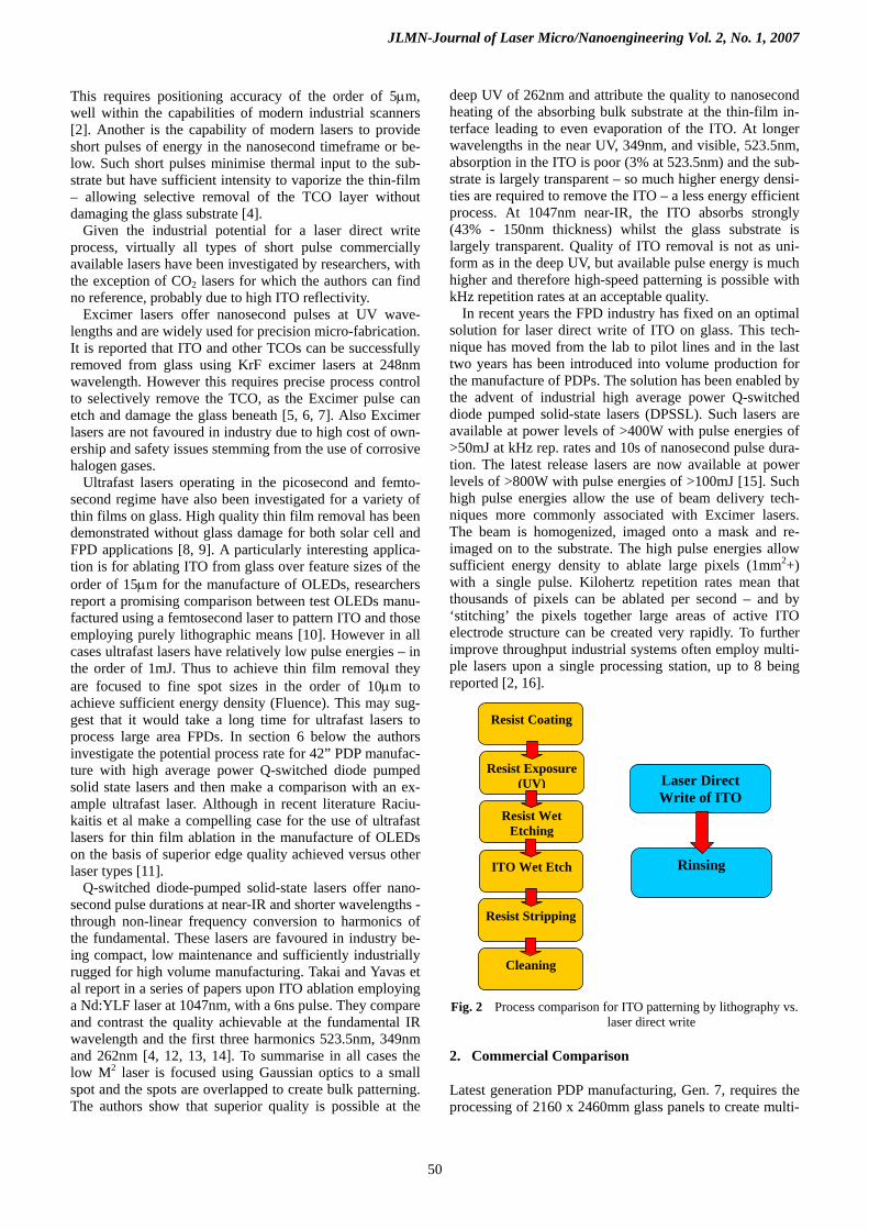
Resist Coating
Resist Exposure (UV)
Resist Wet Etching
ITO Wet Etch
Resist Stripping
Cleaning
Laser Direct Write of ITO
Rinsing
Fig. 2 Process comparison for ITO patterning by lithography vs. laser direct write
2. Commercial Comparison
Latest generation PDP manufacturing, Gen. 7, requires the processing of 2160 x 2460mm glass panels to create multi-
50

JLMN-Journal of Laser Micro/Nanoengineering Vol. 2, No. 1, 2007
ple 42” PDPs per mother panel. The minimum number of process steps required to pattern ITO lithographically is six, and this is shown in figure 2 by comparison with those needed for laser direct write.
As can be seen the laser direct write process requires only 2 process steps versus a minimum of 6 for litho-graphic patterning of ITO. In reality there would probably be more cleaning and rinsing steps for lithography, extend-ing the number of processing stations further. All process-ing stations will have to be large enough to accommodate a Gen. 7 panel with an area of >5m2 thus having a large foot-print.
In addition to size, the required processing stations have a very high capital cost. A commercial stepper, which would be employed to cure the photo-resist using a UV light source, would cost upwards of $12M. This is only a single process station in the lithography sequence. The mask sets for a single PDP design would cost around $1M. A mask writing tool costs upwards of $10M. It is obvious that the lithography process requires very significant in-vestment. By comparison a laser direct write station achieving equivalent TAKT time with multiple lasers might cost under $6M and achieve the same result as at least 5 lithographic processing stations.
Further advantages to laser direct write are that it does not require the use of corrosive etching chemicals. It there-fore offers substantial environmental benefits. It is also a soft tooling process, so is much more flexible than lithog-raphy, requiring only optical mask changes to adjust pixel shape. Finally lithography over such a large area suffers major challenges in achieving uniformity of the cured photo-resist and also subsequent wet etching. This is largely due to the handling issues caused by such large glass mother panels. Consequently yields are not always a high as might be hoped. Laser Direct Write is a much more tolerant process being purely optical, and manufacturers suggest that yields of >99% may be possible in mature mass production [2, 16, 17].
3. Experimental
All substrates were 100nm thick ITO coated on PDP grade glass 2.8mm thick. The laser used was a 400W Starlase AO4 Q-switched DPPSL at the Nd:YAG fundamental wavelength of 1064nm. At 6kHz repetition rate, output pulse energy is 53mJ with pulse duration of 35ns. The Star-lase range of lasers is manufactured exclusively by Power-lase Ltd, UK. The laser was attenuated externally using a proprietary Powerlase unit. The beam was collimated using a Galilean telescope and homogenized by an integrated orthogonal lens array manufactured by LIMO GmbH. Fig-ure 3 below shows measured beam homogeneity from the unit.
X profile
0
50
100
150
200
250
100 200 300 400 500 600 700 800
CCD camera pixel numberr
inte
nsity
[a.u
.]
Fig. 3 Measured homogenised energy profile of the beam
The beam was imaged on to an empirical test mask; this mask plane was relayed to the substrate and demagnified using a Rodenstock f-theta 163mm focal length lens. A HurryScan 25 galvanometric scanner manufactured by Scanlab GmbH was used to scan the beam across the sam-ple. An image plane of 1mm2 was achieved at the work-piece. ITO ablation was assessed using a Nikon LM1500 opti-cal microscope with a PC interface via a 12 Mega pixel camera into Lucia G software. This software allowed mi-croscopic measurements to be made against a Nikon cali-brated standard. Further assessment of the ITO ablation was done using a Scanning Electron Microscope (SEM) at 20kV and an Atomic Force Microscope (AFM). Power measurements were made at the workpiece using a Molectron power meter.
4. Results & Discussion
For single pulse ITO ablation of a large pixel size, optimum laser performance for a Starlase AO4 is at 6 kHz repetition rate. This is the highest rep. rate at which maximum pulse energy of 53mJ at 35ns pulse duration is achieved. There-fore this represents optimal performance for large pixel size, and all experiments are carried out at this setting. Nominal pixel dimensions are 1x1mm, and the empirical mask used creates an electrode structure on the ITO that is illustrative of that in production PDPs. The pixels are ‘stitched’ to-gether to create large area active electrode structures. Through the use of an external Powerlase attenuator the pulse energy reaching the workpiece is accurately con-trolled. It is corroborated by means of a Molectron power meter positioned at the workpiece. Employing a simple square mask to aperture the wings of the homogenised beam, energy transfer efficiency is of the order of 70% from laser output to the workpiece, in good agreement with the literature [16]. More complex masks obviously reduce the energy transfer efficiency but the energy density at the workpiece (fluence in J/cm2) remains constant. The use of a homogeniser and mask creates a nominal flat top profile, therefore the fluence values measured are much more accurate and representative than in cases where Gaussian beam profiles with variable spatial energy pro-files are approximated to uniform energy density. A range of trials is conducted from 1.2-3.4J/cm2 in 0.2 J/cm2 increments in order to determine ablation threshold.
51

JLMN-Journal of Laser Micro/Nanoengineering Vol. 2, No. 1, 2007
Fig. 4 Increasing fluence vs. ITO ablation Figure 4 above shows images of the resulting ITO ablation at increasing fluence. A clear trend emerges from the im-ages: at low fluence the ITO is barely affected, from 1.6J/cm2 onwards structure appears that corresponds with the ripples on the top of the homogenised structure (see figure 3) and more ITO is removed with increasing fluence. As the energy density reaches 2.6J/cm2 the ITO removal becomes very uniform and from 2.8J/cm2 to maximum fluence there is no discernable change in the ablated ITO region. This suggests that above a certain threshold all the ITO is removed and that the process effectively saturates.
Using this visual assessment it is clear that the ITO ablation threshold in this case is 2.8J/cm2. It is also encouraging that the ITO removal is consistent from this point on because it means that the process is reasonably tolerant of energy variation and is therefore well suited for practical industrial use.
the ripples on the top of the homogenised structure (see figure 3) and more ITO is removed with increasing fluence. As the energy density reaches 2.6J/cm
In terms of FPD functionality the ITO must be removed sufficiently to achieve electrical isolation in the patterned regions. Figure 5 below shows a measure of conductivity between two points isolated by a line of pixels 20mm long as shown in figure 4 above. Two interesting effects are ob-served, the first is that electrical isolation is indeed achieved, but at a much lower fluence level than expected – 2J/cm2. We can see from figure 4e that at this energy den-sity there appears to be a significant amount of ITO re-maining. So isolation is achieved well before all the ITO appears to be removed. Secondly conductivity actually rises at low fluence, where figure 4b shows negligible ITO removal. This suggests that the impinging laser pulse is having a significant effect on the properties of the thin-film well below the fluence threshold required for complete removal. This will be explored in subsequent papers.
In terms of FPD functionality the ITO must be removed sufficiently to achieve electrical isolation in the patterned regions. Figure 5 below shows a measure of conductivity between two points isolated by a line of pixels 20mm long as shown in figure 4 above. Two interesting effects are ob-served, the first is that electrical isolation is indeed achieved, but at a much lower fluence level than expected – 2J/cm
2 the ITO removal becomes very uniform and from 2.8J/cm2 to maximum fluence there is no discernable change in the ablated ITO region. This suggests that above a certain threshold all the ITO is removed and that the process effectively saturates.
Using this visual assessment it is clear that the ITO ablation threshold in this case is 2.8J/cm2. It is also encouraging that the ITO removal is consistent from this point on because it means that the process is reasonably tolerant of energy variation and is therefore well suited for practical industrial use.
2. We can see from figure 4e that at this energy den-sity there appears to be a significant amount of ITO re-maining. So isolation is achieved well before all the ITO appears to be removed. Secondly conductivity actually rises at low fluence, where figure 4b shows negligible ITO removal. This suggests that the impinging laser pulse is having a significant effect on the properties of the thin-film well below the fluence threshold required for complete removal. This will be explored in subsequent papers.
0.0
2.0
4.0
6.0
8.0
10.0
12.0
14.0
16.0
1 1.4 1.8 2.2 2.6 3 3.4
Fluence [J/cm2]
Cond
ucta
nce
[mS]
Fig. 5 Conductance vs. fluence for ablated ITO
This result also casts doubt on the assessment of ITO re-moval threshold by purely visual means. As a consequence it is decided to employ other analytical techniques to com-pare with optical microscopy: SEM and AFM. SEM has two possible operational modes, in this case high energy SEM is used; operating at 20kV produces di-rect electron backscatter. The backscatter is greatest from regions of high electron density – therefore conductive materials such as ITO stand out against insulating materials like glass. This should give a good indication at what threshold the ITO is completely removed.
a) 1.2J/cm2 b) 1.4J/cm2
c) 1.6J/cm2 d) 1.8J/cm2
e) 2.0J/cm2 f) 2.2J/cm2
g) 2.4J/cm2 h) 2.6J/cm2
2.8J/cm2
Visual Optimum
i) 2.8J/cm2 j) 3.0J/cm2
k) 3.2J/cm2 l) 3.4J/cm2
52
JLMN-Journal of Laser Micro/Nanoengineering Vol. 2, No. 1, 2007
a) 1.8J/cm2 1.6J/cm2 e) 2.6J/cm2 2.4J/cm2
b) 2.0J/cm2 1.8J/cm2 e) 2.8J/cm2 2.6J/cm2
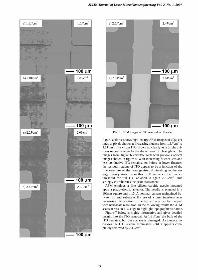
c) 2.2J/cm2 2.0J/cm2 Fig. 6 SEM images of ITO removal vs. fluence
Figure 6 above shows high-energy SEM images of adjacent lines of pixels shown at increasing fluence from 1.6J/cm2 to 2.8J/cm2. The virgin ITO shows up clearly as a bright uni-form region relative to the darker area of clear glass. The images from figure 6 correlate well with previous optical images shown in figure 4. With increasing fluence less and less conductive ITO remains. As before at lower fluences the residual regions of ITO appear to be a function of the fine structure of the homogeniser, diminishing as the en-ergy density rises. From this SEM sequence the fluence threshold for full ITO ablation is again 2.8J/cm2. This strongly corroborates the prior assessment. AFM employs a fine silicon carbide needle mounted upon a piezo-electric actuator. The needle is scanned in a 100μm square and a 15nA nominal current maintained be-tween tip and substrate. By use of a laser interferometer measuring the position of the tip, surfaces can be mapped with nanoscale resolution. In the following results the AFM scans across an ITO edge to highlight topographic variation.
d) 2.4J/cm2 2.2J/cm2
Figure 7 below is highly informative and gives detailed insight into the ITO removal. At 1.8 J/cm2 the bulk of the ITO remains, but the surface is damaged. As fluence in-creases the ITO residue diminishes until it appears com-pletely removed by 2.4J/cm2.
53

JLMN-Journal of Laser Micro/Nanoengineering Vol. 2, No. 1, 2007
a) 1.8J/cm2
e) 2.6J/cm2
Fig. 7 3D AFM scans across an ITO boundary at increasing fluence
Figure 7 also serves to illustrate the precision of this proc-ess; the edge between the virgin ITO and remaining glass substrate clearly defined with the ITO a consistent 100nm above the glass; and a 1μm edge interface in sharp relief. The ablated area is also as flat as the virgin ITO, a further indicator of a selective, precise process.
b) 2.0J/cm2 Combined all this corroboratory data strongly supports the opinion that ITO is completely removed by the laser direct write process. The AFM threshold for ablation is 2.4J/cm2, but given the desire to be conservative for a ro-bust industrial process, we suggest 2.8J/cm2 as determined by SEM and optical microscopy as the optimal value for this example industrial substrate. It also suggests that the SEM is capable of resolving ITO residue of the order of a few nanometres thickness, as this is around the practical resolution limit of the AFM. Figure 7 demonstrates the formation of a nanoscale ridge at the interface between virgin ITO and the laser-processed area. The formation of such a ridge is around the edge of the processed region is identified by several researchers for a variety of lasers at different pulse durations and wave-lengths [4, 8, 12, 13 and 14]. The formation of this ridge is attributed to a thermal material removal mechanism creat-ing molten regions at the extremities of the laser-processed area. These regions are believed to arise as a consequence of surface tension in the melt and lateral vapour pressure from the expanding adjacent vaporising material. The au-thors have corroborated the thermal nature of the material removal mechanism in other work [18].
c) 2.2J/cm2
This ridge been raised as a source of potential concern by industrialists and academics. It is better illustrated by a cross-section profile taken from the AFM as shown in fig-ure 8.
d) 2.4J/cm2
Fig. 8 AFM cross section across interface at 2.6J/cm2
54

JLMN-Journal of Laser Micro/Nanoengineering Vol. 2, No. 1, 2007
From this figure the ridge does indeed appear very pro-nounced. However such analysis can be misleading, and the scale of figures 7 & 8 must be considered. The x-axis is in micrometres, whereas the y-axis is in nanometres. So the y-axis is magnified x1000 more than the x-axis. This is, of course, the nature of a nanoscale surface analysis technique such as AFM, where very small features are heavily magni-fied so they can be perceived. If we consider comparative scaling then the feature is barely perceptible. Figure 9 be-low illustrates such scaling showing both 10:1 and 1:1 axis ratios for a similar ITO cross section.
Fig. 9 Comparative scales of two cross-sections from AFM across the ITO interface
Concerns over the nature of the ridge are also mitigated by the fact that in PDP manufacture the ITO layer is subse-quently coated with 1μm thick MgO, which acts as a stable barrier layer, to prevent erosion of the ITO electrodes by plasma etching during the lifetime of the product [2]. This layer is > 10x thicker than that of the ridge and therefore will effectively seal this feature. Consequently the authors are confident that this process phenomenon will not ad-
versely affect the manufacture or lifetime performance of a PDP made using laser direct write.
5. Case Study
Identifying 2.8J/cm2 as optimum fluence for 100nm ITO ablation allows a case study looking at the application of this technique for the manufacture of PDPs. This seeks to offer an initial estimate of the effective process time to pat-tern each 42” PDP made from a Gen 7 glass mother panel. Table 1 below lists constant parameters and assumptions.
Table 1 Case study parameters
Energy density required (J/cm2) 2.8 Laser rep. rate (kHz) 6
Pulse duration (ns) 35 Optical transmission laser to substrate (%) 52
Mother glass size (mm) 2160 x 2460No. of 42” panels on mother glass 8
42” panel size (mm) 523 x 930 Total load/unload time (s) 90
Laser Duty Cycle (%) 70 Area of PDP patterned (%) 100
It is assumed that a laser direct write processing station would be a hybrid employing both high speed galvanomet-ric scanners to rapidly pattern a limited working area, and X-Y axes to move the glass to enable large area processing. The parameters above represent a conservative assessment of this process. In practice optical transmission can achieve >70%. The figure of 90s for loading and unloading the glass mother panel is also generous given modern auto-mated handling. The laser duty cycle is intended to reflect the need to turn off the scanner assuming a step and repeat methodology is employed between scanning pass and X-Y motion to the next region of ITO. Again this is conservative given that systems integrators have demonstrated tech-niques to process on the fly with constant motion using a ‘bow-tie’ technique – allowing near 100% laser up time [16]. The processing velocity of the scanner is contingent upon the rep. rate of the laser used and the resulting area that can be processed per pulse, and can be back calculated from the data given, each pulse is assumed to be adjacent to but not overlapping the previous - 0% overlap.
Table 2 Case study results
Time to process x1
42” PDP (s)
Laser Pulse Energy
(mJ)
Area/ pulse (mm2)
x1 Laser
x4 Laser
x8 Laser
AO4 53 0.91 138.7 34.7 17.3
AO6 83 1.42 92.6 23.2 11.6
AO8 116 1.99 69.5 17.4 8.7
A commonly cited target for industrial manufacturing of PDP is 45s per 42” PDP panel. This assumes batch process
55

JLMN-Journal of Laser Micro/Nanoengineering Vol. 2, No. 1, 2007
wet etching of the Gen 7 mother panel to produce the 8 sub-panels simultaneously. Looking at Table 2 above shows that a Laser Direct Write processing system employ-ing a single laser would not meet this target. However by using a multiple laser system, and processing the panels concurrently, it is possible to exceed this target by a con-siderable margin. An approach already described in the literature [2, 19]. By way of further comparison, the most promising alter-native laser type for this process may be an ultrafast laser. Attempting the same task using a focussed beam achieving a 20μm diameter spot size at 5kHz would take 441896s or >122 hours to pattern a single 42” panel. Even employing an eight laser system process time would still be > 15 hours, suggesting that ultrafast lasers are not yet suitable for proc-essing such large area substrates.
6. Future Trends
One significant issue is the global shortage of Indium, as its price rises researchers like Satoh et al are investigating alternative thin films such as doped SnO2 for use with laser direct write [1, 19]. Investigations are also underway for removing ITO from flexible substrates like PET, and non-TCO thin films like Mo for solar cell manufacture. This technique is primarily used for the manufacture of large area PDPs, however LCD-TFTs still represent the bulk of the FPD market. There is equal industry pressure to eliminate or reduce the need for lithography in LCD manu-facture. However, the design of LCDs makes it more diffi-cult to employ the laser direct write technique as it stands. This is chiefly due to the fact that ITO layers are usually sputtered on to sensitive organic materials such as colour filters. The process works well for PDP because the glass substrate has a much lower absorption than the ITO layer at 1064nm, therefore leakage through the ITO layer does not adversely affect it. Yavas & Takai measure ITO absorption of only 20% at 1047nm [4]. However if the substrate is more strongly absorbing then there is the potential that the laser process will cause damage, a concern for LCD. Recently however Fukuda et al have demonstrated an ingenious technique that mitigates this problem by intro-ducing the laser at a grazing angle of incidence to the workpiece. Allowing precise control of the ITO absorption and resulting leakage, which may enable this technique to be used successfully for LCD-TFT manufacture as well [20].
7. Conclusions
The authors demonstrate the enormous commercial poten-tial of laser direct write versus wet-etch lithography for the patterning of ITO on glass for the manufacture of PDPs. It is empirically demonstrated that very high quality ITO re-moval can be achieved and an optimum industrial fluence of 2.8J/cm2 is identified for example 100nm thin film using advanced analytical techniques. A case study is performed for the manufacture of 42” PDP panels by laser direct write techniques, using a multiple laser system, and it is demon-strated that process time per panel can potentially be below 20s.
Acknowledgments The authors would like to thank Chris Schild and all at LIMO GmbH for providing a homogeniser and technical assistance. They would also like to thank Marian K. Millar at Heriot Watt University for her invaluable help with the AFM.
References [1] T. Minami: Journal of Semiconductor Science and
Technology, 20 (2005) S35-S44 [2] S. Venkat and C. Dunsky: “Photon Processing in Mi-
croelectronics and Photonics V” Photonics West 2006, San Jose. Proceedings of SPIE Vol. 6106, 610602 (2006)
[3] www.howstuffworks.com [4] O. Yavas and M. Takai: Appl. Phys. Lett. Vol. 73, No.
18 (1998) pp.2558-2560 [5] J. G. Lunney, R. R. O’Neill, K. Schulmeister: Appl.
Phys. Lett. Vol. 59, No. 6 (1991) pp.647-649 [6] T. Szörényi, L. D. Laude, I. Bertóti, Z. Kántor and Z.
Geretovsky: J. Appl. Phys. Vol. 78, No. 10 (1995) pp.6211-6219
[7] P. Rumsby, E. Harvey, D. Thomas and N. Rizvi: SPIE Vol. 3184 (2005)
[8] H-W. Choi, D. Farson, K-R. Kim and S-K. Hong: Proc. Laser Microfabrication Conference, ICALEO 2005, Miami, pp.20-27
[9] J. Hermann et al: J. Applied Surface Science (2005) [10] M. Park et al: J. Optics and Lasers in Engineering 44
(2006) pp.138-146 [11] G. Raciukaitis et al: Proc. Laser Microfabrication Con-
ference, ICALEO 2006, Scottsdale, pp. 165-172 [12] M. Takai, D. Bollmann and K. Haberger: Appl. Phys.
Lett. Vol. 64, No. 19 (1994) pp.2560-2562 [13] O. Yavas, C. Ochiai and M. Takai: Appl. Phys. A
[Suppl.], S875-878 (1999) [14] O. Yavas, M. Takai: J. Appl. Phys., Vol. 85, No. 8
(1999) pp.4207-4212 [15] www.powerlase.com/products/ao8.html [16] P. T. Rumsby: IMID ’02 Digest (2002) [17] J. P. Beouf: J. Phys. D.: Appl. Phys. 36 (2003) R53-
R79 [18] M. Henry, J. Wendland, P.M. Harrison: Laser Micro-
fabrication Conference, ICALEO 2006, Scottsdale, pp. 188-197
[19] R. Usui, R. Satoh et al: Proc. Laser Microfabrication Conference, ICALEO 2005, Miami, pp.13-19
[20] N. Fukuda: Laser Microfabrication Conference, ICALEO 2006, Scottsdale, pp. 179-187
(Received: May 16, 2006, Accepted: February 5, 2007)
56