Nanoscale voxel spectroscopy by simultaneous EELS and EDS ... · spectroscopy (EDS)18–20 and...
7
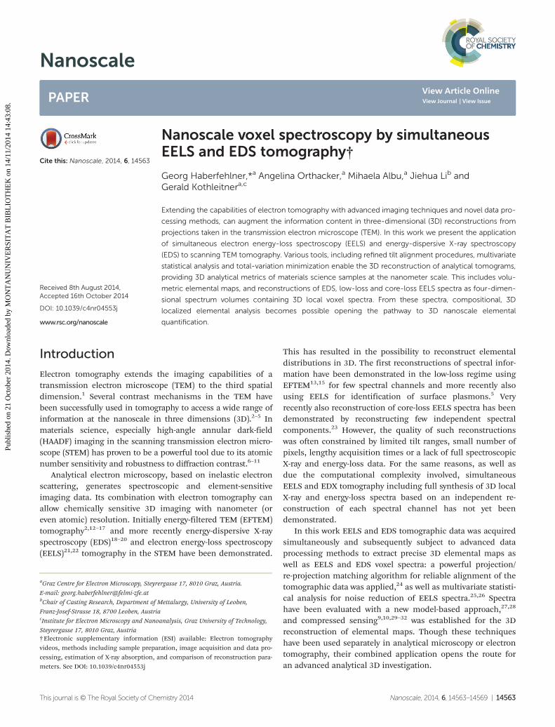
Nanoscale PAPER Cite this: Nanoscale, 2014, 6, 14563 Received 8th August 2014, Accepted 16th October 2014 DOI: 10.1039/c4nr04553j www.rsc.org/nanoscale Nanoscale voxel spectroscopy by simultaneous EELS and EDS tomography† Georg Haberfehlner,* a Angelina Orthacker, a Mihaela Albu, a Jiehua Li b and Gerald Kothleitner a,c Extending the capabilities of electron tomography with advanced imaging techniques and novel data pro- cessing methods, can augment the information content in three-dimensional (3D) reconstructions from projections taken in the transmission electron microscope (TEM). In this work we present the application of simultaneous electron energy-loss spectroscopy (EELS) and energy-dispersive X-ray spectroscopy (EDS) to scanning TEM tomography. Various tools, including refined tilt alignment procedures, multivariate statistical analysis and total-variation minimization enable the 3D reconstruction of analytical tomograms, providing 3D analytical metrics of materials science samples at the nanometer scale. This includes volu- metric elemental maps, and reconstructions of EDS, low-loss and core-loss EELS spectra as four-dimen- sional spectrum volumes containing 3D local voxel spectra. From these spectra, compositional, 3D localized elemental analysis becomes possible opening the pathway to 3D nanoscale elemental quantification. Introduction Electron tomography extends the imaging capabilities of a transmission electron microscope (TEM) to the third spatial dimension. 1 Several contrast mechanisms in the TEM have been successfully used in tomography to access a wide range of information at the nanoscale in three dimensions (3D). 2–5 In materials science, especially high-angle annular dark-field (HAADF) imaging in the scanning transmission electron micro- scope (STEM) has proven to be a powerful tool due to its atomic number sensitivity and robustness to diffraction contrast. 6–11 Analytical electron microscopy, based on inelastic electron scattering, generates spectroscopic and element-sensitive imaging data. Its combination with electron tomography can allow chemically sensitive 3D imaging with nanometer (or even atomic) resolution. Initially energy-filtered TEM (EFTEM) tomography 2,12–17 and more recently energy-dispersive X-ray spectroscopy (EDS) 18–20 and electron energy-loss spectroscopy (EELS) 21,22 tomography in the STEM have been demonstrated. This has resulted in the possibility to reconstruct elemental distributions in 3D. The first reconstructions of spectral infor- mation have been demonstrated in the low-loss regime using EFTEM 13,15 for few spectral channels and more recently also using EELS for identification of surface plasmons. 5 Very recently also reconstruction of core-loss EELS spectra has been demonstrated by reconstructing few independent spectral components. 23 However, the quality of such reconstructions was often constrained by limited tilt ranges, small number of pixels, lengthy acquisition times or a lack of full spectroscopic X-ray and energy-loss data. For the same reasons, as well as due the computational complexity involved, simultaneous EELS and EDX tomography including full synthesis of 3D local X-ray and energy-loss spectra based on an independent re- construction of each spectral channel has not yet been demonstrated. In this work EELS and EDS tomographic data was acquired simultaneously and subsequently subject to advanced data processing methods to extract precise 3D elemental maps as well as EELS and EDS voxel spectra: a powerful projection/ re-projection matching algorithm for reliable alignment of the tomographic data was applied, 24 as well as multivariate statisti- cal analysis for noise reduction of EELS spectra. 25,26 Spectra have been evaluated with a new model-based approach, 27,28 and compressed sensing 9,10,29–32 was established for the 3D reconstruction of elemental maps. Though these techniques have been used separately in analytical microscopy or electron tomography, their combined application opens the route for an advanced analytical 3D investigation. † Electronic supplementary information (ESI) available: Electron tomography videos, methods including sample preparation, image acquisition and data pro- cessing, estimation of X-ray absorption, and comparison of reconstruction para- meters. See DOI: 10.1039/c4nr04553j a Graz Centre for Electron Microscopy, Steyrergasse 17, 8010 Graz, Austria. E-mail: [email protected] b Chair of Casting Research, Department of Mettalurgy, University of Leoben, Franz-Josef-Strasse 18, 8700 Leoben, Austria c Institute for Electron Microscopy and Nanoanalysis, Graz University of Technology, Steyrergasse 17, 8010 Graz, Austria This journal is © The Royal Society of Chemistry 2014 Nanoscale, 2014, 6, 14563–14569 | 14563 Published on 21 October 2014. Downloaded by MONTANUNIVERSITAT BIBLIOTHEK on 14/11/2014 14:43:08. View Article Online View Journal | View Issue
Transcript of Nanoscale voxel spectroscopy by simultaneous EELS and EDS ... · spectroscopy (EDS)18–20 and...
Nanoscale
PAPER
Cite this: Nanoscale, 2014, 6, 14563
Received 8th August 2014,Accepted 16th October 2014
DOI: 10.1039/c4nr04553j
www.rsc.org/nanoscale
Nanoscale voxel spectroscopy by simultaneousEELS and EDS tomography†
Georg Haberfehlner,*a Angelina Orthacker,a Mihaela Albu,a Jiehua Lib andGerald Kothleitnera,c
Extending the capabilities of electron tomography with advanced imaging techniques and novel data pro-
cessing methods, can augment the information content in three-dimensional (3D) reconstructions from
projections taken in the transmission electron microscope (TEM). In this work we present the application
of simultaneous electron energy-loss spectroscopy (EELS) and energy-dispersive X-ray spectroscopy
(EDS) to scanning TEM tomography. Various tools, including refined tilt alignment procedures, multivariate
statistical analysis and total-variation minimization enable the 3D reconstruction of analytical tomograms,
providing 3D analytical metrics of materials science samples at the nanometer scale. This includes volu-
metric elemental maps, and reconstructions of EDS, low-loss and core-loss EELS spectra as four-dimen-
sional spectrum volumes containing 3D local voxel spectra. From these spectra, compositional, 3D
localized elemental analysis becomes possible opening the pathway to 3D nanoscale elemental
quantification.
Introduction
Electron tomography extends the imaging capabilities of atransmission electron microscope (TEM) to the third spatialdimension.1 Several contrast mechanisms in the TEM havebeen successfully used in tomography to access a wide range ofinformation at the nanoscale in three dimensions (3D).2–5 Inmaterials science, especially high-angle annular dark-field(HAADF) imaging in the scanning transmission electron micro-scope (STEM) has proven to be a powerful tool due to its atomicnumber sensitivity and robustness to diffraction contrast.6–11
Analytical electron microscopy, based on inelastic electronscattering, generates spectroscopic and element-sensitiveimaging data. Its combination with electron tomography canallow chemically sensitive 3D imaging with nanometer (oreven atomic) resolution. Initially energy-filtered TEM (EFTEM)tomography2,12–17 and more recently energy-dispersive X-rayspectroscopy (EDS)18–20 and electron energy-loss spectroscopy(EELS)21,22 tomography in the STEM have been demonstrated.
This has resulted in the possibility to reconstruct elementaldistributions in 3D. The first reconstructions of spectral infor-mation have been demonstrated in the low-loss regime usingEFTEM13,15 for few spectral channels and more recently alsousing EELS for identification of surface plasmons.5 Veryrecently also reconstruction of core-loss EELS spectra has beendemonstrated by reconstructing few independent spectralcomponents.23 However, the quality of such reconstructionswas often constrained by limited tilt ranges, small number ofpixels, lengthy acquisition times or a lack of full spectroscopicX-ray and energy-loss data. For the same reasons, as well asdue the computational complexity involved, simultaneousEELS and EDX tomography including full synthesis of 3D localX-ray and energy-loss spectra based on an independent re-construction of each spectral channel has not yet beendemonstrated.
In this work EELS and EDS tomographic data was acquiredsimultaneously and subsequently subject to advanced dataprocessing methods to extract precise 3D elemental maps aswell as EELS and EDS voxel spectra: a powerful projection/re-projection matching algorithm for reliable alignment of thetomographic data was applied,24 as well as multivariate statisti-cal analysis for noise reduction of EELS spectra.25,26 Spectrahave been evaluated with a new model-based approach,27,28
and compressed sensing9,10,29–32 was established for the 3Dreconstruction of elemental maps. Though these techniqueshave been used separately in analytical microscopy or electrontomography, their combined application opens the route foran advanced analytical 3D investigation.
†Electronic supplementary information (ESI) available: Electron tomographyvideos, methods including sample preparation, image acquisition and data pro-cessing, estimation of X-ray absorption, and comparison of reconstruction para-meters. See DOI: 10.1039/c4nr04553j
aGraz Centre for Electron Microscopy, Steyrergasse 17, 8010 Graz, Austria.
E-mail: [email protected] of Casting Research, Department of Mettalurgy, University of Leoben,
Franz-Josef-Strasse 18, 8700 Leoben, AustriacInstitute for Electron Microscopy and Nanoanalysis, Graz University of Technology,
Steyrergasse 17, 8010 Graz, Austria
This journal is © The Royal Society of Chemistry 2014 Nanoscale, 2014, 6, 14563–14569 | 14563
Publ
ishe
d on
21
Oct
ober
201
4. D
ownl
oade
d by
MO
NT
AN
UN
IVE
RSI
TA
T B
IBL
IOT
HE
K o
n 14
/11/
2014
14:
43:0
8.
View Article OnlineView Journal | View Issue

Two ways to examine analytical electron tomography datahave been pursued in this work. These are outlined in Fig. 1.In a STEM, tilt angle resolved spectrum images were acquired,recording EDS, low-loss and core-loss EELS spectra simul-taneously for each pixel. This results in four-dimensional (4D)datasets, where each dataset consists of two spatial, oneenergy and a fourth tilt angle dimension. In our first approachtowards 3D chemical imaging, 2D elemental maps have beenextracted for each tilt angle from the spectrum images (A1 inFig. 1), giving tilt-dependent EELS and EDS chemical infor-mation for every element under consideration. By tomographicreconstruction (A2 in Fig. 1) each tilt-dependent map was usedto reconstruct a three-dimensional element-specific volume. Inour second approach EELS and EDS spectra were directlyreconstructed from the spectrum image tilt series by doingone reconstruction for each individual spectral channel (B inFig. 1), yielding 4D datasets – spectrum volumes – that consistof three spatial and one energy dimension. 3D local voxelspectra could then be extracted and analyzed to access localchemical information on a spectral rather than an imagebasis.
Results & discussion
The procedures involved in analytical electron tomography aredemonstrated on an Al–5 wt% Si alloy with 50 ppm Na and
6100 ppm Yb. Modification and refinement of eutectic Si inAl–Si alloys by trace elements is a widely used method toimprove mechanical properties of casting alloys.33–37 Neverthe-less the modification and refinement mechanisms are still amatter of debate and require understanding of the elementaldistribution down to the atomic level.35 A needle shapedsample, suitable for tomography, was prepared from thesurface of the Al–Si sample using focused ion beam (FIB)milling38,39 (see ESI†).
Analytical electron tomography experiments were per-formed on a probe-corrected FEI Titan3 G2 60-300 microscopewith an X-FEG Schottky field-emission electron source oper-ated at 300 kV (see ESI† for details). The microscope isequipped with a Gatan Imaging Filter (GIF) Quantum40 and aFEI Super-X EDS detector, consisting of four separate silicondrift detectors.41 The microscope setup allows fast parallelacquisition of EDS data as well as of low-loss and core-lossEELS spectra using the dual-EELS capacity of the GIFQuantum.42–44 Thanks to this experimental setup spectrumimages of about 100 × 200 pixels with a pixel size of 1 nmcould be acquired every 5° over a tilt range from −75° to +80°.Fig. 2 shows HAADF STEM images acquired at different tiltangles and EDS and EELS spectra from single pixels in theprojections.
Fig. 2 (a) HAADF STEM images from tilt series. (b) Single pixel low-lossEELS spectra. (c) Single pixel core-loss EELS spectra (original spectra areshown as histogram, PCA-treated spectra as solid lines) (d) Single pixelEDS spectra. Spectra are taken from the locations indicated by (1), (2)and (3) in (a). In (c) & (d) ionization edges and X-ray absorption lines areindicated. Spurious signals from the microscope and sample holder (Cu)are shown in brackets. The Cu signal is strong at high tilt angles (−70°)as a part of the scattered electrons hit the sample support.
Fig. 1 Principles of analytical electron tomography showing the twoapproaches (A & B) pursued in this work.
Paper Nanoscale
14564 | Nanoscale, 2014, 6, 14563–14569 This journal is © The Royal Society of Chemistry 2014
Publ
ishe
d on
21
Oct
ober
201
4. D
ownl
oade
d by
MO
NT
AN
UN
IVE
RSI
TA
T B
IBL
IOT
HE
K o
n 14
/11/
2014
14:
43:0
8.
View Article Online

The tilt series alignment was carried out via HAADF STEMimages, acquired together with the analytical data. The align-ment process, which requires all projections to be registered toa common tilt axis located in the center of the projections, wasa two-stage process. We started with an initial coarse align-ment using filtered cross-correlation between neighboringimages for first estimates of the shift parameters. These shiftparameters were then refined in several iterations using projec-tion/re-projection matching. Similar methods have beendescribed previously and have shown to provide a reliablealignment.24,45 In our workflow, a temporary reconstructionwith the current alignment parameters is calculated, which isthen re-projected at the orientations of the acquired projec-tions. The shift between these re-projections and the acquiredprojections is determined using filtered cross-correlation withsub-pixel accuracy.46 To calculate the position of the tilt axis,rotational centers were calculated for each sinogram by centerof mass methods.47 The shift and rotational alignments weredone alternatingly, cycling through 10 iterations. This provideda set of alignment parameters, which was subsequentlyapplied to all acquired analytical data.
A further challenge in the reconstruction arises from thelow signal-to-noise ratio in core-loss EELS data, for edgesbeyond 1000 eV as for the material investigated (Yb-M45:1528 eV, Al-K: 1560 eV, Si-K: 1839 eV). The short pixel times inaddition to low ionization cross-sections render the spectralprocessing with respect to background removal or thicknessdeconvolution problematic. Furthermore, the Yb-M45 edge isoverlapping with the Al-K edge, which complicates a separ-ation of the net signal of those two edges.
Principal components analysis (PCA) has been shown to beable to overcome noise problems in EELS spectra.22,25,26 Weapply weighted PCA,26 adapted to the dominant Poissoniannoise in our EELS spectra (see ESI including Fig. S1†).Examples for such spectra are shown in Fig. 2b(2) super-imposed with the original data. Noise reduction using PCA wasnecessary for further processing of spectral data. In untreatedspectra the noise was too high to allow reliable extraction ofthe background and element specific signals in particular con-cerning separation of contributions from Yb and Al. For extrac-tion of elemental maps from EELS spectrum images a model-based fitting approach was used.28 The spectrum is modelledusing a background, described with a power-law function andionization edges, given by Hartree-Slater cross-sections. Pluralscattering can be included in the model by convolution of thesingle-scattering core-loss model with the low-loss spectrum.Furthermore the low-loss spectrum was used for modelling theelectron-loss near-edge structure (ELNES) by an iterative refine-ment of ELNES intensities. To extract elemental maps fromprojections, PCA-treated core-loss spectra and the corres-ponding low-loss spectra were used (see ESI includingFig. S2†). The extracted EELS elemental maps correspond tothe extracted signal normalized by the elemental cross-sections.
For extraction of EDS maps also a model-based approachwas used, describing the background with a Kramers-model.48
After identification of the X-ray lines, Gaussian peaks werefitted for each line family and the integral from the wholeseries was used to generate the element-specific signal. Thefitting approach is useful in particular for extraction of Al-ele-mental maps as the Al K-lines (Al-Kα: 1.49 keV) are very closeto the Yb M-lines (Yb-Mα: 1.52 keV). For Si the K-lines (Si-Kα:1.74 keV) and for Yb the L-lines (Yb-Lα: 7.41 keV) were used.The extracted EDS elemental maps correspond to the sum ofX-ray counts for a specific element. In our setup, the extractedintensity of the elemental maps displayed a strong angulardependence due to shadowing of X-rays by the sample holder.This was compensated by normalizing the projections with thesummed intensity from each elemental map at the respectivetilt. This was possible since effects of X-ray absorption in thesample could be neglected due to the small sample size (seeESI including Fig. S3 and Table S1†).
The 3D elemental maps were reconstructed with a total vari-ation (TV) minimization algorithm. For comparison recon-structions with the simultaneous iterative reconstructiontechnique (SIRT) were also carried out. TV minimizationdenotes a variant of compressed sensing.49,50 It is assumedthat the image (or volume) gradient is sparse, i.e. is zero atmost locations. Because of the materials chemistry and thesharp interfaces between the different phases in the sample,the assumption was justified. For TV minimization theproblem
minu[Rn
X
i
kDiuk2 þ μ
2kAu� bk22 ð1Þ
was solved.51 In this formulation the first term is the isotropicTV norm of the image or volume vector u. Diu is the local gra-dient vector at the position i in three dimensions. This 3Dimplementation of the algorithm provides more reliable recon-structions compared to previous implementations of TV mini-mization where the gradient Diu was usually calculated along 2dimensions.29–32 The second term in (1) represents a least-squares optimization of the linear equation system given bythe projection geometry. b is the measurement vector contain-ing all projection data. A is the projection operator mappingfrom the image or volume vector u to a projection vector.52 µ isa weighting factor between the two terms in the optimizationand needs to be adapted to the noise level in the projections(see ESI including Fig. S4† for a comparison of reconstructionsusing 2D and 3D algorithms and different weightingfactors µ).
Slices through 3D EELS elemental maps of the major con-stituents of the sample are displayed in Fig. 3a for both SIRTand TV minimization. The same slices through 3D EDSelemental maps are depicted in Fig. 3b. TV minimization pro-vided sharp interfaces in the reconstruction and allowedsimple segmentation of the reconstruction based on absolutethreshold values using the Otsu threshold criterion.53 Fig. 3cand d and ESI Videos S1 and S2† show surface rendered viewsof segmented 3D EELS and EDS elemental maps respectively.
Nanoscale Paper
This journal is © The Royal Society of Chemistry 2014 Nanoscale, 2014, 6, 14563–14569 | 14565
Publ
ishe
d on
21
Oct
ober
201
4. D
ownl
oade
d by
MO
NT
AN
UN
IVE
RSI
TA
T B
IBL
IOT
HE
K o
n 14
/11/
2014
14:
43:0
8.
View Article Online

TV minimization applied to the reconstruction of elementalmaps was very efficient regarding noise reduction. In the caseof silicon, it is easily possible to distinguish regions with ahigher Si-concentration from regions with a lower Si-concen-tration, where also Yb is present. Good agreement can beobserved between the reconstructions from EELS and EDSdata.
To extract more information about local material compo-sitions we reconstructed 3D local EDS and EELS spectra foreach voxel (cf. approach B in Fig. 1). For EELS plural scatteringwas removed,54 so single-scattering spectra could be recon-structed. Depending on the energy regime either Fourier-log(low-loss) or Fourier-ratio (high-loss) deconvolution wascarried out. EELS core-loss spectra had been PCA treatedbeforehand. For the reconstruction each spectral channel wastreated as an independent tilt series and was reconstructedusing a multiplicative SIRT algorithm with 30 iterations (seeESI†). This process resulted in physically meaningful recon-structions, as every voxel spectrum represents the local singlescattering probability. In the EDS case, again spectra normal-ized to compensate shadowing effects were reconstructed (seeESI†). Since X-ray intensities are proportional to the probabilityof X-ray creation along the beam path through the sample, thereconstructed voxel spectra contain information about the 3Dlocal X-ray creation probability. Fig. 4 shows single-voxelspectra (voxel size: 1 nm3) from different locations in the
sample. Different absorption edges and X-ray lines as well aschanges in their relative intensity can be clearly distinguished.
Being able to reconstruct the 3D elemental maps and localvoxel spectra allows combining the information from both.
Fig. 3 (a) Orthogonal slices through reconstructions of the Yb M45-edge, the Si K-edge and the Al K-edge from EELS data. (b) Orthogonal slicesthrough reconstructions of the Yb L-line, the Si K-line and the Al K-line from EDS data. (c) Surface rendered views of the segmented volume of theYb M45-edge, the Si K-edge and the Al K-edge and an overlay of the three segmented volumes. (d) Surface rendered views of the segmented volumeof the Yb L-line, the Si K-line and the Al K-line and an overlay of the three segmented volumes.
Fig. 4 Reconstructed single voxel spectra (voxel size: 1 nm3). (a) Single-scattering low-loss EELS spectra, (b) single-scattering core-loss EELSspectra (PCA treated) and (c) EDS spectra. Ionization edges and majorX-ray lines are indicated. Spectra are extracted (1) from an Yb-rich pre-cipitate, (2) from a Si-rich region, (3) from Al.
Paper Nanoscale
14566 | Nanoscale, 2014, 6, 14563–14569 This journal is © The Royal Society of Chemistry 2014
Publ
ishe
d on
21
Oct
ober
201
4. D
ownl
oade
d by
MO
NT
AN
UN
IVE
RSI
TA
T B
IBL
IOT
HE
K o
n 14
/11/
2014
14:
43:0
8.
View Article Online

Using all reconstructed data we sum 3D voxel spectra overspecific regions defined by masks created from the 3D EDSelemental maps. To reduce the impact of interfaces betweenthe different materials, the boundaries of the masks wereremoved by applying 3D morphological erosion operators.These 3D masks and EDS and EELS voxel spectra summedover the different regions are shown in Fig. 5. This providesspectra with high signal to noise ratio but which contain onlyinformation about a single phase in three dimensions. Suchmatrix-free spectra cannot be analyzed from 2D spectrumimages as spectra of localized phases are also affected by othermaterials over the thickness of the sample.
With voxel spectra being available, relative phase compo-sitions could be derived, harnessing the strengths of therespective EELS and EDS quantification schemes, yet encoun-tering some typical issues, associated with overlapping signalsor inaccurate sensitivity factors. Quantification of the Yb-richprecipitates (Fig. 5a) gave Al : Si : Yb compositions of at%43 : 47 : 10 in EELS and at% 48 : 35 : 16 for EDS (see ESI†). Inthe present case the main limitation are overlapping Yb-M andAl-K edges and X-ray lines. Furthermore for the EELS case theM45-edge of Yb is not well modelled by the Hartree-Slatercross-section model. EDS quantification is based on k-factors,which are not known with high accuracy. Despite the observedcompositional variation between the techniques, these values
give a fair estimate about the relative composition. This alsoshows the usefulness of simultaneous EELS and EDS analysis,as the complementarity of the two techniques serves to vali-date results from one technique by the other.
Conclusions
In the present work simultaneous analytical EELS and EDStomography for 3D nanoscale chemically sensitive microscopywas established. While conventional tomographic techniques,such as HAADF STEM tomography, can only provide indi-cations about chemistry, 3D elemental maps can provideunambiguous elemental identification and reveal compo-sitional changes. Elemental identification removes manyuncertainties in the interpretation of tomograms. We demon-strated the feasibility of reconstructing spectrum volumes forboth EELS and EDS reconstructing each spectral channel indi-vidually. These four-dimensional datasets contain local voxelspectra, which allow the local access of different regions in thesample. In this way a 3D matrix-free analysis of confinedphases, such as nanoparticles or precipitates, becomes possi-ble. This is an important step towards reliable compositionalquantification in 3D space. We have shown that data proces-sing methods, such as projection/re-projection matching,multivariate statistical analysis and compressed sensing, canenable reliable reconstructions of analytical tomograms, evenfrom data limited in terms of pixel time, number of pixels andthe number of spectrum images.
Simultaneous EELS and EDS tomography allows verificationof one technique by the other, but it will also be useful whensome elements in a sample are easier to detect by one tech-nique or the other. Furthermore linking analytical tomographywith complementary techniques, such as atom probe tomogra-phy55 will allow a deeper understanding of materials andtechniques.
Apart from elemental quantification EELS tomography hasthe potential for extraction of local electrical and optical pro-perties or chemical fingerprinting in three dimensions. Thelow-loss spectrum contains a large amount of informationabout material properties, in the core-loss spectrum ELNESanalysis can provide information about the chemical state in3D. These methods will be applicable to a wide range ofmaterials, essentially to all applications where 3D nanometerresolution is required in combination with chemical sensi-tivity. Examples are all types of embedded nanoparticles, core/shell structures, precipitation studies or the investigation ofdopants.
Another interesting goal of analytical electron tomography– next to reliable quantification – will be to combine chemicalsensitivity with 3D atomic resolution. The main challenges liein the long acquisition times compared to HAADF STEM,where atomic resolution tomography has already been demon-strated. Spectrum images with high enough signal to noiseratio need to be recorded, while limiting beam damage andsample drift during image acquisition.
Fig. 5 Local core-loss EELS and EDS spectra summed over differentregions of the volume: (a) summed over Yb-rich precipitates, (b)summed over Si-rich regions, (c) summed over the Al-matrix withoutthe surface layer. (1) Shows the masks over which spectra are summed,(2) shows the core-loss EELS spectra, (3) shows EDS spectra, the inset in(3) shows a zoom to the low-energy region from 0.3 keV to 1.3 keVIonization edges and X-ray lines are indicated. Absorption lines arisingdue to the instrument and sample support (Cu, Fe, Co) are written inbrackets. Ga and O are present due to Ga-ion implantation duringsample preparation and surface oxidation.
Nanoscale Paper
This journal is © The Royal Society of Chemistry 2014 Nanoscale, 2014, 6, 14563–14569 | 14567
Publ
ishe
d on
21
Oct
ober
201
4. D
ownl
oade
d by
MO
NT
AN
UN
IVE
RSI
TA
T B
IBL
IOT
HE
K o
n 14
/11/
2014
14:
43:0
8.
View Article Online

Acknowledgements
This research has received funding from the European Unionwithin the 7th Framework Program [FP7/2007–2013] undergrant agreement no. 312483 (ESTEEM2) and from the AustrianForschungsförderungsgesellschaft (FFG) in the OPTIMAT-STRUCT project. We thank Evelin Fisslthaler, Johanna Kraxnerand Werner Grogger from FELMI-ZFE Graz and Peter Schuma-cher from Chair of Casting Research, University of Leoben fordiscussions and advise as well as Paul Thomas, Ray Twestenand Bernd Kraus from Gatan for providing software prototypesfor EELS and EDS analysis. Open-source software code hasbeen used: The TV minimization solver TVAL3 (http://www.caam.rice.edu/~optimization/L1/TVAL3/), the tomographicreconstruction toolbox ASTRA (http://sourceforge.net/projects/astra-toolbox/) and the spectral data analysis toolkit Hyperspy(http://hyperspy.org/).
Notes and references
1 P. A. Midgley and R. E. Dunin-Borkowski, Nat. Mater., 2009,8, 271–280.
2 G. Möbus, R. C. Doole and B. J. Inkson, Ultramicroscopy,2003, 96, 433–451.
3 A. J. Koster, R. Grimm, D. Typke, R. Hegerl, A. Stoschek,J. Walz and W. Baumeister, J. Struct. Biol., 1997, 120, 276–308.
4 J. S. Barnard, J. Sharp, J. R. Tong and P. A. Midgley, Science,2006, 313, 319.
5 O. Nicoletti, F. de la Peña, R. K. Leary, D. J. Holland,C. Ducati and P. A. Midgley, Nature, 2013, 502, 80–84.
6 P. A. Midgley and M. Weyland, Ultramicroscopy, 2003, 96,413–431.
7 S. Van Aert, K. J. Batenburg, M. D. Rossell, R. Erni andG. Van Tendeloo, Nature, 2011, 470, 374–377.
8 M. C. Scott, C.-C. Chen, M. Mecklenburg, C. Zhu, R. Xu,P. Ercius, U. Dahmen, B. C. Regan and J. Miao, Nature,2012, 483, 444–447.
9 B. Goris, S. Bals, W. Van den Broek, E. Carbó-Argibay,S. Gómez-Graña, L. M. Liz-Marzán and G. Van Tendeloo,Nat. Mater., 2012, 11, 930–935.
10 B. Goris, A. De Backer, S. Van Aert, S. Gómez-Graña,L. M. Liz-Marzán, G. Van Tendeloo and S. Bals, Nano Lett.,2013, 13, 4236–4241.
11 C.-C. Chen, C. Zhu, E. R. White, C.-Y. Chiu, M. C. Scott,B. C. Regan, L. D. Marks, Y. Huang and J. Miao, Nature,2013, 496, 74–77.
12 G. Möbus and B. J. Inkson, Appl. Phys. Lett., 2001, 79,1369–1371.
13 M. H. Gass, K. K. K. Koziol, A. H. Windle and P. A. Midgley,Nano Lett., 2006, 6, 376–379.
14 I. Florea, O. Ersen, C. Hirlimann, L. Roiban, A. Deneuve,M. Houlle, I. Janowska, P. Nguyen, C. Pham and C. Pham-Huu, Nanoscale, 2010, 2, 2668–2678.
15 G. Haberfehlner, P. Bayle-Guillemaud, G. Audoit,D. Lafond, P. H. Morel, V. Jousseaume, T. Ernst andP. Bleuet, Appl. Phys. Lett., 2012, 101, 063108.
16 M. Weyland and P. A. Midgley, Microsc. Microanal., 2003, 9,542–555.
17 R. D. Leapman, E. Kocsis, G. Zhang, T. L. Talbot andP. Laquerriere, Ultramicroscopy, 2004, 100, 115–125.
18 Z. Saghi, X. Xu, Y. Peng, B. Inkson and G. Möbus, Appl.Phys. Lett., 2007, 91, 251906.
19 K. Lepinay, F. Lorut, R. Pantel and T. Epicier, Micron, 2013,47, 43–49.
20 A. Genc, L. Kovarik, M. Gu, H. Cheng, P. Plachinda,L. Pullan, B. Freitag and C. Wang, Ultramicroscopy, 2013,131, 24–32.
21 K. Jarausch, P. Thomas, D. N. Leonard, R. Twesten andC. R. Booth, Ultramicroscopy, 2009, 109, 326–337.
22 L. Yedra, A. Eljarrat, R. Arenal, E. Pellicer, M. Cabo,A. López-Ortega, M. Estrader, J. Sort, M. D. Baróe,S. Estradé and F. Peiró, Ultramicroscopy, 2012, 122, 12–18.
23 L. Yedra, A. Eljarrat, J. M. Rebled, L. López-Conesa, N. Dix,F. Sánchez, S. Estradé and F. Peiró, Nanoscale, 2014, 6,6646–6650.
24 T. Uusimäki, G. Margaris, K. Trohidou, P. Granitzer,K. Rumpf, M. Sezen and G. Kothleitner, Nanoscale, 2013, 5,11944–11953.
25 M. Bosman, M. Watanabe, D. T. L. Alexander andV. J. Keast, Ultramicroscopy, 2006, 106, 1024–1032.
26 F. de la Peña, M.-H. Berger, J.-F. Hochepied, F. Dynys,O. Stephan and M. Walls, Ultramicroscopy, 2011, 111, 169–176.
27 J. Verbeeck and S. Van Aert, Ultramicroscopy, 2004, 101,207–224.
28 P. J. Thomas and R. D. Twesten, Microsc. Microanal., 2012,18, 968–969.
29 Z. Saghi, D. J. Holland, R. Leary, A. Falqui, G. Bertoni,A. J. Sederman, L. F. Gladden and P. A. Midgley, Nano Lett.,2011, 11, 4666–4673.
30 B. Goris, W. Van den Broek, K. J. Batenburg,H. Heidari Mezerji and S. Bals, Ultramicroscopy, 2012,113, 120–130.
31 R. Leary, Z. Saghi, P. A. Midgley and D. J. Holland, Ultra-microscopy, 2013, 131, 70–91.
32 B. Goris, M. A. Van Huis, S. Bals, H. W. Zandbergen,L. Manna and G. Van Tendeloo, Small, 2012, 8, 937–942.
33 J. H. Li, M. Z. Zarif, G. Dehm and P. Schumacher, Philos.Mag., 2012, 92, 3789–3805.
34 S. Haro-Rodríguez, R. E. Goytia-Reyes, D. K. Dwivedi,V. H. Baltazar-Hernández, H. Flores-Zúñiga and M. J. Pérez-López, Mater. Des., 2011, 32, 1865–1871.
35 J. H. Li, M. Z. Zarif, M. Albu, B. J. McKay, F. Hofer andP. Schumacher, Acta Mater., 2014, 72, 80–98.
36 K. Nogita, H. Yasuda, K. Yoshida, K. Uesugi, A. Takeuchi,Y. Suzuki and A. K. Dahle, Scr. Mater., 2006, 55, 787–790.
37 K. Nogita, H. Yasuda, M. Yoshiya, S. D. McDonald,K. Uesugi, A. Takeuchi and Y. Suzuki, J. Alloys Compd.,2010, 489, 415–420.
Paper Nanoscale
14568 | Nanoscale, 2014, 6, 14563–14569 This journal is © The Royal Society of Chemistry 2014
Publ
ishe
d on
21
Oct
ober
201
4. D
ownl
oade
d by
MO
NT
AN
UN
IVE
RSI
TA
T B
IBL
IOT
HE
K o
n 14
/11/
2014
14:
43:0
8.
View Article Online

38 N. Kawase, M. Kato, H. Nishioka and H. Jinnai, Ultramicro-scopy, 2007, 107, 8–15.
39 P. Bleuet, G. Audoit, J.-P. Barnes, J. Bertheau, Y. Dabin,H. Dansas, J.-M. Fabbri, B. Florin, P. Gergaud, A. Grenier,G. Haberfehlner, E. Lay, J. Laurencin, R. Serra andJ. Villanova, Microsc. Microanal., 2013, 19, 726–739.
40 A. Gubbens, M. Barfels, C. Trevor, R. Twesten, P. Mooney,P. Thomas, N. Menon, B. Kraus, C. Mao and B. McGinn,Ultramicroscopy, 2010, 110, 962–970.
41 P. Schlossmacher, D. O. Klenov, B. Freitag and H. S. vonHarrach, Microsc. Today, 2010, 18, 14–20.
42 P. Longo and R. D. Twesten,Microsc. Today, 2013, 21, 28–33.43 G. Kothleitner, M. J. Neish, N. R. Lugg, S. D. Findlay,
W. Grogger, F. Hofer and L. J. Allen, Phys. Rev. Lett., 2014,112, 085501.
44 G. Kothleitner, W. Grogger, M. Dienstleder and F. Hofer,Microsc. Microanal., 2014, 20, 678–686.
45 H. Winkler and K. A. Taylor, Ultramicroscopy, 2006, 106,240–254.
46 M. Guizar-Sicairos, S. T. Thurman and J. R. Fienup, Opt.Lett., 2008, 33, 156–158.
47 S. G. Azevedo, D. J. Schneberk, J. P. Fitch and H. E. Martz,IEEE Trans. Nucl. Sci., 1990, 37, 1525–1540.
48 H. A. Kramers, Philos. Mag., 1923, 46, 836.49 E. J. Candes, J. Romberg and T. Tao, IEEE Trans. Inf. Theory,
2006, 52, 489–509.50 D. L. Donoho, IEEE Trans. Inf. Theory, 2006, 52, 1289–
1306.51 C. Li, W. Yin, H. Jiang and Y. Zhang, Comput. Optim. Appl.,
2013, 56, 507–530.52 W. J. Palenstijn, K. J. Batenburg and J. Sijbers, J. Struct.
Biol., 2011, 176, 250–253.53 N. Otsu, IEEE Trans. Syst. Man Cybern., 1979, 9, 62–66.54 R. F. Egerton, Rep. Prog. Phys., 2009, 72, 016502.55 A. Grenier, S. Duguay, J. P. Barnes, R. Serra,
G. Haberfehlner, D. Cooper, F. Bertin, S. Barraud,G. Audoit, L. Arnoldi, E. Cadel, A. Chabli and F. Vurpillot,Ultramicroscopy, 2014, 136, 185–192.
Nanoscale Paper
This journal is © The Royal Society of Chemistry 2014 Nanoscale, 2014, 6, 14563–14569 | 14569
Publ
ishe
d on
21
Oct
ober
201
4. D
ownl
oade
d by
MO
NT
AN
UN
IVE
RSI
TA
T B
IBL
IOT
HE
K o
n 14
/11/
2014
14:
43:0
8.
View Article Online