Modeling Voltage-Controlled Resistors and Capacitors … App Note_Modeling Voltage... ·...
8
APPLICATION NOTE Modeling Voltage-Controlled Resistors and Capacitors in PSpice The ANL_MISC.LIB library file contains subcircuit models for voltage-controlled reactances and admittances. These can be used to make voltage-controlled resistors and capacitors. In this application note, we will illustrate the usage of voltage controlled impedance for controlling Q of a series RLC filter network and changing the frequency of a Wien bridge oscillator.
Transcript of Modeling Voltage-Controlled Resistors and Capacitors … App Note_Modeling Voltage... ·...

APPLICATION NOTE
Modeling Voltage-Controlled Resistors and Capacitors in PSpice
The ANL_MISC.LIB library file contains subcircuit models for voltage-controlled reactances and admittances.
These can be used to make voltage-controlled resistors and capacitors. In this application note, we will illustrate
the usage of voltage controlled impedance for controlling Q of a series RLC filter network and changing the
frequency of a Wien bridge oscillator.

APPLICATION NOTE
1
Introduction The ANL_MISC.LIB library file contains subcircuit models for voltage-controlled reactances and admittances.
These can be used to make voltage-controlled resistors and capacitors. In this application note, we will illustrate
the usage of voltage controlled impedance for controlling Q of a series RLC filter network and changing the
frequency of a Wien bridge oscillator.
Note: This modeling technique is not applicable to capacitances whose values change slowly. It applies to cases
where the capacitance changes very quickly between constant values.
Controlling Q of a Series RLC Filter Network using Voltage-Controlled Resistor In most circuits the value of a resistor is fixed during simulation. While the value can be made to change through a
fixed sequence of values, for a set of simulations using parametric sweep, a voltage-controlled resistor can be
made to change its value dynamically during a simulation. This is illustrated by the circuit shown in Figure 1. The
circuit uses a voltage- controlled resistor, X_VCRes. This special resistor is defined using the ZX subcircuit
from ANL_MISC.LIB. This subcircuit consists of two controlled sources and employs an external reference
component that is sensed. The output impedance equals the value of the control voltage times the reference.
Here, we will use Rref, a 50 ohm resistor as our reference. As a result, the output impedance is seen by the
circuit as a floating resistor equal to the value of Vcontrol times the resistance value of Rref. In our circuit, the
control voltage value is stepped from 0.5 volt to 2 volts in 0.5 volt steps. Therefore, the resistance between
nodes 3 and 0 varies from 25 ohms to 100 ohms in 25 ohm-steps.
Figure 1 Variable Q RLC Circuit

APPLICATION NOTE
2
Variable Q RLC Network The first and second connections to the ZX subcircuit are the control input, followed by a connection to the
reference component and then, finally, the two connections for the floating impedance.
The Variable Q RLC circuit is simulated for 4ms (Run to time) along with parametric sweep, varying Vin
(Vcontrol) from 0.5V to 2V in steps of 0.5V. Select PSpice – Edit Simulation Profile for the simulation settings
window.
Using a 0.5 ms wide pulse, the transient analysis of the circuit shows how the ringing differs as the Q is varied
by X_VCRes. Figure 2 shows the input pulse and the voltage across the capacitor C1. Comparing the four output
waveforms, we can see the most pronounced ringing occurs whenX_VCRes has the lowest value and the Q is
greatest. Any signal source can be used to drive our voltage-controlled impedance. If we had used a sinusoidal
control source instead of a staircase, the resistance would have varied dynamically during the simulation.
Voltage-Controlled Wien Bridge Oscillator In this example, we will use a voltage-controlled capacitor to adjust the frequency of oscillation for a Wien bridge
oscillator.
A simplified operational amplifier (opamp) is created using a voltage-controlled voltage source EAmp (an E
device). Node 1 is the plus input, node 2 is the minus input and node 4 is the output of the opamp.
Eamp 4 0 Value {V(1,2) * 1E6} A voltage divider network provides negative feedback to the amplifier. The closed-loop gain of the opamp must be
at least 3, for oscillations to occur. This is because the Wien bridge attenuates the output by 1/3 at the frequency
of oscillation. The back-to-back Zener diodes limit the gain of the opamp, as the oscillations build, so that
saturation does not occur.
APPLICATION NOTE
3
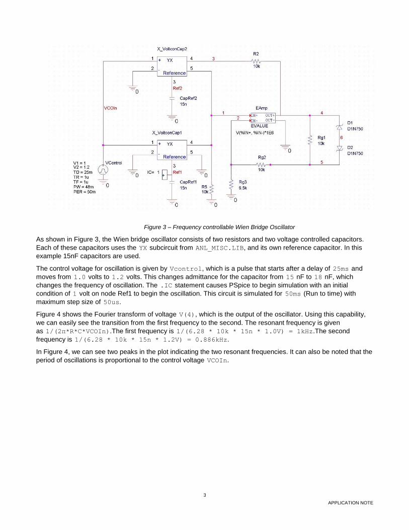
Figure 3 – Frequency controllable Wien Bridge Oscillator
As shown in Figure 3, the Wien bridge oscillator consists of two resistors and two voltage controlled capacitors.
Each of these capacitors uses the YX subcircuit from ANL_MISC.LIB, and its own reference capacitor. In this
example 15nF capacitors are used.
The control voltage for oscillation is given by Vcontrol, which is a pulse that starts after a delay of 25ms and
moves from 1.0 volts to 1.2 volts. This changes admittance for the capacitor from 15 nF to 18 nF, which
changes the frequency of oscillation. The .IC statement causes PSpice to begin simulation with an initial
condition of 1 volt on node Ref1 to begin the oscillation. This circuit is simulated for 50ms (Run to time) with
maximum step size of 50us.
Figure 4 shows the Fourier transform of voltage V(4), which is the output of the oscillator. Using this capability,
we can easily see the transition from the first frequency to the second. The resonant frequency is given
as 1/(2π*R*C*VCOIn).The first frequency is 1/(6.28 * 10k * 15n * 1.0V) = 1kHz.The second
frequency is 1/(6.28 * 10k * 15n * 1.2V) = 0.886kHz.
In Figure 4, we can see two peaks in the plot indicating the two resonant frequencies. It can also be noted that the
period of oscillations is proportional to the control voltage VCOIn.

APPLICATION NOTE
4
Figure 4 - Frequency controllable Wien Bridge oscillator output
Modeling Voltage-Variable Capacitors Some time designers need to model a voltage variable capacitor. The following example circuit file describes a
test circuit that contains a voltage-variable capacitor. This capacitor is constructed by way of a TABLE function
embedded in the VALUE extension to the G (voltage-controlled current source) device. This model is a better
representation of a varicap device than the commonly used YX device. The Probe plot in Figure 6 shows
capacitance versus controlling voltage for a voltage-variable capacitor similar to 1N4155.
From the D device capacitance equations
CJ = CJO * (1 + Vr/Vj)**-M
where
CJO = zero-bias junction capacitance
CJO = p-n potential
M = p-n grading coefficient
Cj is junction capacitance for reverse voltage Vr.
This can be modelled using a voltage-controlled current source with voltage controlled by table-based voltage-
controlled current source.
.subckt tablecap 1 2 PARAMS: C4 = 1pf, M = 0.5, VJ = 1.0
.Ecopy 3 6 1 2 1.0
.Vsense 0 6 0v

APPLICATION NOTE
5
.Cref 3 0 {C4 * pwr(vj+4, M)} ; computes CJO from C4
.Hsense 10 0 Vsense 1.0 ; converts I(Cref) to V(10)
.Gout 1 2 VALUE = ; capacitance/voltage modeling
.+ {v(10)/pwr(TABLE(v(1,2), 1, 1, 60, 60)+VJ, M)}
.ends
Figure 5 - Voltage-variable capacitor test circuit
Figure 6 - Voltage-variable capacitor simulation result
APPLICATION NOTE
6
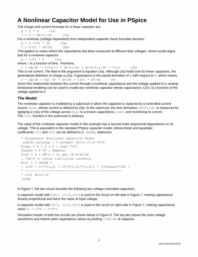
A Nonlinear Capacitor Model for Use in PSpice The charge and current formulas for a linear capacitor are:
Q = C * V (1a)
I = C * dV(t)/dt (1b)
For a nonlinear (voltage-dependent) time-independent capacitor these formulae become:
Q = ò C(V) * dV (2a)
I = C(V) * dV/dt (2b)
This applies to cases where the capacitance has been measured at different bias voltages. Some would argue
that for a nonlinear capacitor,
Q = C(V) * V (3a)
where V is a function of time. Therefore,
I = dQ/dt = C(V(t)) * dV(t)/dt + dC(V(t))/dt * V(t) (3b)
This is not correct. The flaw in this argument is equation (3a). Although (1a) holds true for linear capacitors, the
generalized definition of charge is (2a). Capacitance is the partial derivative of Q with respect to V; which means
I = dQ/dt = ¶Q/ ¶V * dV/dt = C(V) * dV/dt (4)
Given this relationship between the current through a nonlinear capacitance and the voltage applied to it, analog
behavioral modeling can be used to model any nonlinear capacitor whose capacitance, C(V), is a function of the
voltage applied to it.
The Model
The nonlinear capacitor is modeled by a subcircuit in which the capacitor is replaced by a controlled current
source, Gout, whose current is defined by (2b). In the subcircuit, the time derivative, dV(t)/dt, is measured by
applying a copy of the voltage across Gout to a known capacitance, Cref, and monitoring its current.
The C(V) function in the subcircuit is arbitrary.
The value of the nonlinear capacitor model in this example has a second order polynomial dependence on its
voltage. This is equivalent to the standard PSpice capacitor model, whose linear and quadratic
coefficients, VC1 and VC2, can be defined in a .MODEL statement.
* Polynomial Nonlinear Capacitor Model
.subckt polycap 1 2 params: C0=1u C1=0 C2=0
Ecopy 3 6 1 2 1.0 ; copy V(t)
Vsense 0 6 0V ; Ammeter
Cref 3 0 1.0E-6 ; to get 1E-6*dv/dt
; *1E-6 to avoid ridiculous currents
Gout 1 2 VALUE =
+ {(C0 + C1*V(1,2) + C2*V(1,2)*V(1,2)) * I(Vsense)*1E6 }
* ------------------------------------ -------------
* C(V) dV(t)/d
.ends
In Figure 7, the two circuit simulate the following two voltage controlled capacitors:
A capacitor model with C0=1, C1=2,C2=0 is used in the circuit on left-side in Figure 7, making capacitance
linearly proportional and twice the value of input voltage.
A capacitor model with C0=1, C1=2,C2=0 is used in the circuit on right-side in Figure 7, making capacitance
value Co + C*V + C*V*V.
Simulation results of both the circuits are shown below in Figure 8. The top plot shows the input voltage
waveforms and bottom plots capacitance values by plotting I*dV/dT of capacitor.

APPLICATION NOTE
7
Figure 7 - Voltage-variable capacitor test circuit
Figure 8 - Voltage-variable capacitor simulation result
© Copyright 2016 Cadence Design Systems, Inc. All rights reserved. Cadence, the Cadence logo, and Spectre are registered trademarks of Cadence Design Systems, Inc. All others are properties of their respective holders.