Microprocessor Lab manual 1 - Webnodefiles.msaqib.webnode.com/200000050-01005017cf/Microprocessor...
50
UMM AL-QURA UNIVERSITY LAB MANUAL Microprocessors By:__________________ College of Computer Information Systems Engineering Department of Computer Engineering Umm Al-Qura University
Transcript of Microprocessor Lab manual 1 - Webnodefiles.msaqib.webnode.com/200000050-01005017cf/Microprocessor...
UMM AL-QURA UNIVERSITY
LAB MANUAL
Microprocessors
By:__________________
College of Computer Information Systems Engineering Department of Computer Engineering
Umm Al-Qura University

List of Experiments
Interface Experiments Using 8086 Microprocessor Kits &
Application Boards
� Flight 8086 Training Board 3
� Conducting Simple I/O Operations Using Flight 86 Training Kit 12
� Generating Timing Sequences 19
� Analog To Digital & Digital To Analog Conversion 29
� Controlling Dc Motors 36
� Interfacing A Hyper Terminal To The Flight 86 Kit 41
Mini Project
3
Flight 8086 Training Board
Objective
The aim of this lab experiment is to familiarize the students with Flight 8086 training board.
Equipment
Flight 8086 training board, PC with Flight86 software, download cable.
Tasks to be Performed
� Connecting the 8086 training board to PC (using COM1 port)
� Study of different commands provided by the training board
� Program entry, execution and debugging
� Assembling and disassembling of a program
� Displaying the contents of registers and memory locations
� Modifying registers and memory contents
� Single-step execution and breakpoint insertion
� Downloading & uploading a program file
� Running simple programs to perform the following operations:
1. Arithmetic operations
2. Finding the smallest/largest number from a given list of numbers
3. Searching for a given number in a list of numbers
Experiment
1

4
1.1 Background
The FLIGHT 86 Trainer System is designed to simplify the teaching of the 8086 CPU and some of its commonly used peripherals. It can be linked to most PCs with a simple serial line, so that code may be assembled and debugged in a supportive software environment before being downloaded into the RAM on the board. The board itself may then be linked to other peripheral devices. A block diagram of this mode of operation is shown in Figure 1.1.
Figure 1.1: Block Diagram of the FLIGHT-86 Trainer System
Once downloaded, the code may be executed and examined in a system which is accessible to the user. Data may be manipulated on the board and the effects viewed on the PC. The software which handles this two-way transfer is supplied with the board, in the form of a monitor program resident on the board in EPROM, and a disk containing the "host" software for the PC.
1.2 Connecting the Training Board to PC
Figure 1.2 shows the FLIGHT-86 Trainer Board layout. The first step is to connect the serial socket (P3) on the training board to COM1 in the PC using RS232 cable. Next, connect the power cable to the power supply connector (P6). Finally, load the program F86GO.BAT on the PC. This should run and report the amount of RAM and EPROM on the FLIGHT-86 board, before returning the prompt as shown in Figure1.3.
1.3 Commands Provided by Flight-86
A ‘-’ prompt on the screen means that the host is ready to accept a command. Table1.1 gives a summary of the commands that will be used during this experiment.

5
Figure 1.2: Layout of the FLIGHT-86 Training Board
Loading FLIGHT86 host program, please wait...
FLIGHT86 Controller Board, Host Program Version 2.1
Press ? and Enter for help - waiting for controller board response...
ROM found at F000:C000 to F000:FFFF Flight Monitor ROM version 2.0
RAM found at 0000:0000 to 0000:FFFF
-
Figure 1.3: Starting Message of the FLIGHT-86 Training Board

6
Table 1.1: Summary of some commands provided by FLIGHT-86
KEY PARAMETER DESCRIPTION
ESC Press the Escape button to stop the current command
X Resets the training board
Q Terminates running of the board software and returns control to the operating system
? [command letter] Help
R [register] Allows the user to display or change the content of a register
M [W][segment:] address1 [address2] Allows the user to display or change one or more memory locations
A [[segment:] address] Allows the user to write 8086 assembly code directly into the training board
Z [[V] [segment:] address1 [address2]] Disassemble command
G [[segment:] address] Allows the user to execute code that has been downloaded into RAM
B ? | R | S [segment:] address Allows the user to Display/Clear/Set break points inside his code
S [R][[segment:] address] Allows the user to step through code one instruction at a time
: [drive:\path] filename Loads an Extended Intel Hex file from disk into the memory of the training board
1.4 The First Program
Assembling a Program (Command A)
The assemble command (A [segment:] address) allows you to type in 8086 assembly code, and this code will be assembled and stored into the board memory. The following example shows you how to write a simple program using this command
Example 1.1: Using the assemble command, write a program that will add the content of two memory locations (words) and store the result in a third memory location.
1. Start the line assembler at the desired address by entering A 0050:0100 (Note that the origin address for user RAM on the FLIGHT-86 is 0050:0100)
2. The FLIGHT-86 responds by echoing the address 0050:0100

7
3. Now enter the assembly code one instruction at a time hitting ENTER after
each instruction 4. Each time, the FLIGHT-86 responds by echoing the next address 5. When you are done exit from the line assembler by pressing ESC button The screen will now look like
A 0050:0100 0050:0100 DW 0002 0050:0102 DW 0003 0050:0104 DW 0000 0050:0106 MOV AX,[0100] 0050:0109 ADD AX,[0102] 0050:010D MOV [0104], AX 0050:0111 INT 5 0050:0113 -
Disassembling a Program (Command Z)
You can examine what you have entered using the disassemble command. If you type Z 0050:0100 0111, then the content of the memory locations between the addresses 0050:0100 and 0050:0111 will be disassembled as follows:
0050:0100 02 00 ADD AL, [BX+SI] 0050:0102 03 00 ADD AX, [BX+SI] 0050:0104 00 00 ADD [BX+SI], AL 0050:0106 A1 01 00 MOV AX,[0100] 0050:0109 03 06 02 01 ADD AX,[0102] 0050:010D 89 06 04 01 MOV [0104], AX 0050:0111 CD 05 INT 5
The HEX numbers between the addresses and the instructions represent the opcodes of the disassembled instructions. Notice that memory words entered as DW directives have been disassembled as ADD instructions with different parameters. This is because the values of these memory words are equivalent to the opcode of the ADD instruction with the shown parameters.
Running a Program (Command G)
To run the above program enter G 0050:0106 and press the ENTER key. The program will now run, load the word at address 0050:0100 into AX, add the content of the word at address 0050:0102 to the content of AX, store the result into the word at

8
address 0050:0104, and terminate. Note that the instruction INT 5 is responsible for terminating the program.
Displaying/Modifying Memory Locations (Command M)
To test the result of the above program enter M W 0050:0104 and press the Enter key. This will display the memory word at address 0050:0104 where the result of the above program is stored. Exit from this command by pressing the ESC key.
Let’s now change the content of the memory words stored at addresses 0050:0100 and 0050:0102. At the command prompt ‘-’, enter M W 0050:0100 and press the Enter key. The content of the memory word at address 0050:0100 is displayed. To change the content of this memory location, enter a HEX number (say 0005) and press the Enter key. The content of the next memory location is displayed. Enter another HEX number (say 0007) and press the Enter key. When the content of the next memory location is displayed, press the ESC key to go back to the command prompt. These steps are shown below:
-M W 0050:0100 0050:0100 0002 0005 0050:0102 0003 0007 0050:0104 0005 -
Now run the program again and test the content of the memory word at address 0050:0104.
Breakpoint Insertion (Command B)
This command is intended for debugging user code. A breakpoint is an INT 3 instruction inserted at an opcode position. The original opcode at this address is saved. When the code is executed it runs normally, at full speed, until it reaches this location. Then, original opcode is restored and the registers, address and first opcode byte are displayed.
As an example, enter the command B S 0050:010D and press the Enter key. This will set a breakpoint at address 0050:010D in the previous program (i.e. a breakpoint is set at the instruction MOV [0104], AX). Now, run the program using the command G 0050:0100. Notice that the program terminates and the message “Monitor breakpoint at 0050:010D” is displayed. This means that the execution of the program stopped at location 0050:010D. You can resume the execution of the program using the command G, but let us first modify the content of register AX. At the command prompt ‘-’, enter the command R AX and press the Enter key. This will display the content of AX which is 000C (i.e. 0005+0007). Modify this value by entering 0001 next to 000C and press the Enter key then ESC to go back to the command prompt.

9
Now, continue the execution of the program from address 0050:010D using the command G 0050:010D. Check the content of memory word at address 0050:0104.
The previous steps are shown below:
-B S 0050:010D -G 0050:0100 Monitor Breakpoint at 0050:010D -R AX AX 000C 0001 BX 0000 -G 0050:010D User Break at 0050:0111 -M W 0050:0104 0050:0104 0001 0050:0106 00A1 -
Single-Step Execution (Command S)
This command is provided to allow the user to step through code one instruction at a time for debugging purposes. The display will be the next instruction address and opcode byte with, optionally, registers content. Once the command has started, pressing the Enter key will execute the next instruction. As an example, enter the command S R 0050:0100 and press the Enter key. This will execute the first instruction and terminate with registers content shown on the screen. When you press Enter again, the next instruction is executed. Continue pressing the Enter key until all instructions in the program get executed, or press the ESC key to terminate the command.
1.5 Writing a Program Using Assembler on a PC
In the pervious section, we have used the assemble command to write and load simple assembly instructions into the board memory. However, for more sophisticated applications, you need to write and assemble programs on a PC before downloading them into the board memory. For this purpose, you need the following programs:
� MASM: as the assembler and linker
� EXE2BIN: to convert from and executable file into a binary file
� BIN2HEX: to convert the binary file into an INTEL HEX file for download to the FLIGHT-86

10
Example 1.2: Write a program to search for a given number in a list of numbers. You should define the list as a sequence of memory bytes labeled with the letter A. The number to be searched is passed through register DL. When the program terminates, BX should contain the index of the number if it is found in the list.
COMSEG SEGMENT BYTE PUBLIC 'CODE' ASSUME CS:COMSEG, DS:COMSEG, ES:COMSEG, SS:COMSEG ORG 0100h start: MOV AX, CS MOV DS, AX ; Set the data segment MOV BX, 0 ; Set BX to index of the 1st element in ; the list L1: CMP BX, 8 ; if BX exceeds the indices of the l ist JZ L2 ; then end the search CMP DL, A[BX] ; if the number is found in the list JZ L2 ; then end the search INC BX ; else increment BX JMP L1 L2: INT 5 ; terminate the program A DB 4 DB 2 DB 7 DB 6 DB 3 DB 5 DB 1 DB 8 COMSEG ENDS END start
Using any text editor on the PC enter the previous code. The code shown in bold is required for every program using MASM, and can be thought of as a template. Now, save this file with any name (say search.asm). Using the Assembler, i.e. MASM, assemble and link this file to produce SEARCH.EXE, and using EXE2BIN create the binary code file search.bin. Now, using BIN2HEX, convert this binary file to the Intel hex format file search.hex. Finally load the HEX file into the board memory using the command “:search.hex”. Note, you may need to specify the drive and the path of the file if it is not in the same directory as the F86GO software (e.g. :C:\MyProjects\Search.hex).
To run this program, first load the required number into DX using the command R DX. Next, run the program using the command G 0050:0100. Finally, use the command R BX to check result of the search (i.e. the value of BX represents the index of the given number in the list).

11
These steps are shown below.
-R DX DX 0000 0003 SP 0500 -G 0050:0100 User Break at 0050:011A -R BX BX 0004 -
Exercises
1.1. Modify the program in Example 1.1 to perform the four basic operations: addition, subtraction, multiplication, and division. The required operation is specified by loading DX with the appropriate value (i.e. 1 for addition, 2 for subtraction, 3 for multiplication, and 4 for division).
1.2. Write a program to find the smallest number from a given list of numbers. Load this program into the FLIGTH-86 and test it.

12
Conducting Simple I/O
Operations Using Flight 86
Training Kit
Objective
The aim of this lab experiment is to conduct simple I/O operations, reading state of switches and turning on/off LEDs provided on the Application Board, by programming 8255 PPI chip.
Equipment
FLIGHT-86 training board, Application Board, PC with Flight86 software, download cable
Tasks to be Performed
� Interfacing the Application Board to the FLIGHT-86 training board.
� Conducting the following experiments
1. To read the state of a switch (on/off), and to output a signal to turn (on/off) an LED
2. Generate a mod 16 counter and display the output on LEDs. 3. Controlling the operation of the LEDs based on the state of a
particular switch.
Experiment
2

13
2.1 Background
The FLIGHT-86 training board ‘talks’ to the Application Board by means of an Input/Output (I/O) device (i.e. 8255 PPI). This device is quite intelligent, and can perform input, output, and handshaking. However, before it will carry out any of these tasks, it must be told what is required of it. For I/O, it consists of three 8-bit ports. These ports can be set up as input or output ports.
Telling the PPI device how to perform is known as INITIALISATION. Thus, the first code we run after power up or reset, must be one which initializes the 8255. This little code will be required for every experiment.
In this experiment you will learn how to interface the Application Board to the FLIGHT-86 training board, program the 8255 PPI chip, and conduct simple I/O operations.
2.2 The Application Board
Figure 2.1 shows the layout of the Application Board that will be used to carryout a number of experiments. This board incorporates a wide array of electronic devices such as digital switches, LED displays, temperature, light, and optical position/speed sensors, a heater, a DC motor, an LED bar-graph, and a potentiometer. A screw terminal is also provided for external analog input.
The Application Board has two I/O ports (one for input and one for output) connected to a parallel socket (P1). The Processor output port connects to Port-A on the Application Board, and the state of the output port is always displayed on the 8-colored LEDs. This port can be used to control the motor (forward and reverse) and/or the heater. When not in use for these functions, the output port can be used to drive the Digital-to-Analog Converter (D/A). On the other hand, the processor input port connects to Port-B on the Application Board. This port can be used to read the 8-bit DIP switch, or the output of the Analog-to-Digital Converter (A/D), or the output of the D/A comparator, and/or the output of the speed sensing infrared detector.
The operation of the devices on the Application Board is controlled by means of the MODE SWITCHES. There are 6 mode switches divided into two groups (SW2 and SW4). Each switch enables/disables a certain device as shown in Table 2.1.

14
Figure 2.1: Layout of the Application Board
Table 2.1: Mode Switches
Group Switch Operation
SW2
1 Enables either the 8-bit DIP switch or the Analog-to-Digital Converter (ADC)
2 Enables/disables the MOTOR
SW4
1 Enables/disables the speed sensor
2 Enables/disables the Digital-to-Analog Converter (DAC)
3 Enables/Disables the heater
4 Enables/Disables the BARGRAPH

15
2.3 Programming the 8255 PPI Chip
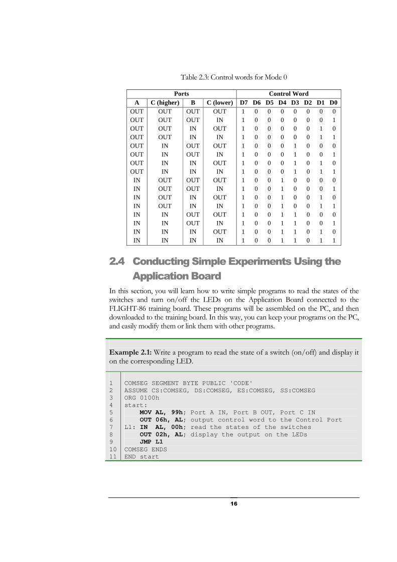
The 8255 is a general-purpose parallel I/O interfacing device. It provides 24 I/O lines organized as three 8-bit I/O ports labeled A, B, and C. In addition to these three ports, a third port (Control) is used to program the chip. Each of the ports, A or B, can be programmed as an 8-bit input or output port. Port C can be divided in half, with the topmost or bottommost four bits programmed as inputs or outputs. Individual bits of a particular port cannot be programmed. In the FLIGTH-86 training board, the 8255 PPI chip is interfaced to two parallel port sockets P1 and P2. In each socket, each one the four ports (A, B, C, and Control) has an individual address as shown in Table 2.2.
Table 2.2: 8255 port addresses
Port Activity allowed Actual port address
P1 P2 Port A Port B Port C Control
Read/Write Read/Write Read/Write Write only
00 01 02 03 04 05 06 07
The 8255 PPI chip can be programmed to operate in three modes:
� Mode 0 Basic Input/Output
� Mode 1 Strobed Input/Output
� Mode 2 Bi-directional bus (not available on FLIGHT-86)
There is also a bit set/reset mode that allows individual bits of port C to be set or reset for control purposes.
In this experiment, you will learn how to initialize the 8255 PPI chip to operate in Mode 0. To learn about programming the 8255 PPI chip in other modes you can refer to your text book.
Mode 0 gives the simplest form of I/O possible, where no ‘handshaking’ is required. Data is simply read from or written to the specified port. Any one of the ports A, B, C (upper half), and C (lower half) can be set individually as input or output ports. This is done by sending a control byte to the Control Port. The 16 possible control words are shown in Table 2.3. Notice that D7, D6, D5, and D2 are fixed for this mode. For example, to set the three ports as output ports, you need to send the control word 80h to the Control port using the following set of instructions:
MOV AL, 80H ; load AL with the control word 80H
OUT 06H, AL ; send this control word to port 60H
; (i.e. the Control port)
16
Table 2.3: Control words for Mode 0
Ports Control Word A C (higher) B C (lower) D7 D6 D5 D4 D3 D2 D1 D0
OUT OUT OUT OUT OUT OUT OUT OUT
IN IN IN IN IN IN IN IN
OUT OUT OUT OUT
IN IN IN IN
OUT OUT OUT OUT
IN IN IN IN
OUT OUT
IN IN
OUT OUT
IN IN
OUT OUT
IN IN
OUT OUT
IN IN
OUT IN
OUT IN
OUT IN
OUT IN
OUT IN
OUT IN
OUT IN
OUT IN
1 0 0 0 0 0 0 0 1 0 0 0 0 0 0 1 1 0 0 0 0 0 1 0 1 0 0 0 0 0 1 1 1 0 0 0 1 0 0 0 1 0 0 0 1 0 0 1 1 0 0 0 1 0 1 0 1 0 0 0 1 0 1 1 1 0 0 1 0 0 0 0 1 0 0 1 0 0 0 1 1 0 0 1 0 0 1 0 1 0 0 1 0 0 1 1 1 0 0 1 1 0 0 0 1 0 0 1 1 0 0 1 1 0 0 1 1 0 1 0 1 0 0 1 1 0 1 1
2.4 Conducting Simple Experiments Using the
Application Board
In this section, you will learn how to write simple programs to read the states of the switches and turn on/off the LEDs on the Application Board connected to the FLIGHT-86 training board. These programs will be assembled on the PC, and then downloaded to the training board. In this way, you can keep your programs on the PC, and easily modify them or link them with other programs.
Example 2.1: Write a program to read the state of a switch (on/off) and display it on the corresponding LED.
1 2 3 4 5 6 7 8 9 10 11
COMSEG SEGMENT BYTE PUBLIC 'CODE' ASSUME CS:COMSEG, DS:COMSEG, ES:COMSEG, SS:COMSEG ORG 0100h start: MOV AL, 99h ; Port A IN, Port B OUT, Port C IN OUT 06h, AL ; output control word to the Control Port L1: IN AL, 00h ; read the states of the switches OUT 02h, AL ; display the output on the LEDs JMP L1 COMSEG ENDS END start

17
Lines 4 and 5 in the above code initialize the 8255 PPI chip in Mode 0, such that ports A and C are set as input ports while port B is set as an output port. Then, the program enters a continuous loop that reads the states of the switches into AL and displays them on the LEDs. Reading the states of the switches (line 7) is done through port A (00h), while displaying the output on the LEDs (line 8) is done through port B (02h).
Example 2.2: Write a program to generate modulo 16 counter and display the output on the LEDs.
1 2 3 4 5 6 7 8 9 10 11 12 13 14 15 16 17 18
COMSEG SEGMENT BYTE PUBLIC 'CODE' ASSUME CS:COMSEG, DS:COMSEG, ES:COMSEG, SS:COMSEG ORG 0100h start: MOV BL, 16 MOV AL, 99h ; Port A IN, Port B OUT, Port C IN OUT 06h, AL ; output control word to the Control Port MOV AX, 0 ; initialize the counter to 0 L1: OUT 02h, AL ; display the counter on the LEDs MOV CX, 0FFFh ; delay loop L2: LOOP L2 INC AL ; increment the counter DIV BL ; AH = AL mod 16 MOV AL, AH MOV AH, 0 JMP L1 COMSEG ENDS END start
The previous code starts as usual by initializing the 8255 PPI chip (lines 6 and 7). The counter is initialized in line 8. Line 9 displays the counter on the LEDs through port B (02h). Then, the program enters a delay loop (lines 10 to 12) before incrementing the counter in line 13. Since a module 16 counting is required, the counter (i.e. AX) is divided by 16 and the remainder is loaded back into AX (lines 14 to 16). Notice that instruction in line 14 divides AX by 16, leaving the quotient in AL and the remainder in AH.

18
Exercises
2.1. Write a program to generate the following based on the state of a particular switch
Switch 1 : ON Generate a mod 8 counter and display it on LEDs
OFF Switch off all LEDs
Switch 2 : ON Generate a mod 256 counter and display it on LEDs
OFF Switch off all LEDs
Switch 3 : ON Light LEDs one after another one at a time in a sequence from left to right (from first LED to Last LED). When one LED is on, all other LEDs must be switched off. (i.e., shifting bit ‘1’ from left to right). Repeat this cycle until the switch 3 is turned OFF
Switch 4 : ON Repeat the above from last LED to the first
2.2. Write a program to add 2 four-bit numbers and display the result on the LEDs. The two numbers are entered through the 8-DIP switch provided on the Application Board (i.e. each 4 switches represent one number).
19
Generating Timing
Sequences
Objective
The aim of this lab experiment is to generate timing sequences using software delays and by programming 8253 Programmable Interval Timer (PIT) chip.
Equipment
Flight 8086 training board, the Application Board, PC with Flight86 software, download cable
Tasks to be Performed
� Generate time delays using software delays and 8253 PIT chip.
� Use generated delays to turn ON/OFF LEDs for specific amounts of time
� Generate waveforms of different frequencies, and observe them on an oscilloscope/logic analyzer.
� Interface a simple relay driver circuit to 8255 port and switch ON/OFF a device for a specific amount of time.
Experiment
3

20
3.1 Background
It is often necessary to control how long certain actions last. This can be achieved using software delays, or more accurately by the use of a timer (i.e. 8253 PIT chip). In this experiment, you will learn how to generate time delays using both software delays and 8253 PIT chip. Also, you will learn how to use time delays to control the operation of some devices (e.g. LEDs and Relays), and to generate periodical waveforms of different frequencies.
3.2 Software Delays
The easiest way to generate delays is a software delay. If we create a program which loops around itself for a fixed number of times, then the time taken by this program on a given processor with a specific clock rate will be almost the same each time the program is executed. All we have to do is to write this loop such that it takes 1 second. Then, by calling this loop n times, we generate a delay of n seconds. Notice that the time taken by the loop does not need to be 1 second. For example, a loop that takes 0.25 seconds to execute, can be called 4×n times (i.e. n/0.25) to generate a delay of n seconds. The question now is how to determine the time taken by a loop. This can be answered by the following example.
Example 3.1: Calculate the total time taken by the following loop.
MOV CX, 8000h ; load CX with a fixed value 8000h (32768) L1: DEC CX ; decrement CX, loop if not zero JNZ L1
From the 8086 data sheets, we find that DEC CX requires 2 clock cycles and JNZ requires 16 clock cycles. Thus, the total number of clock cycles required by these two instructions is 18 clock cycles.
Since the FLIGHT-86 board is running at 14.7456/3 MHz, 1 clock cycle will take 3/14.7456 microseconds, and 18 clock cycles will take 54/14.7456 microseconds. Thus, the total time taken by the loop is 32768 × (54/14.7456 × 10-6) = 0.12 seconds
The previous loop requires 0.12 seconds. Thus, this loop needs to be executed almost 8 times to generate a delay of 1 second. The following example shows how to use this loop inside a program to turn ON/OFF an LED for specific amounts of time.

21
Example 3.2: Write a program to turn ON an LED for 3 seconds, then turn it OFF for another 3 seconds, and repeat this cycle.
COMSEG SEGMENT BYTE PUBLIC 'CODE' ASSUME CS:COMSEG, DS:COMSEG, ES:COMSEG, SS:COMSEG ORG 0100h Start: MOV AL, 99h ; initialize 8255 ports: OUT 06h, AL ; A and C in, B out MOV AL, 01h ; set bit 0 in AL to 1 ON_OFF: OUT 02h, AL ; turn on/off LED 0 MOV DL, 25 ; delay of 25*0.12 = 3 sec CALL Delay XOR AL, 01h ; complement bit 0 in AL JMP ON_OFF Delay PROC L1: MOV CX, 8000h L2: DEC CX JNZ L2 DEC DL JNZ L1 RET Delay ENDP COMSEG ENDS END Start
Run the above program on the FLIGHT-86 board and estimate the ON/OFF time of LED 0. What you conclude about the accuracy of the software delays?
3.3 Time Delays Using the 8253 PIT Chip
Software delays are the easiest way to generate time-delays, as they do not require any additional hardware. However, software delays are not accurate especially for long delays. Therefore, timers like the 8253 PIT chip are used to generate accurate delays. Figure 3.1 shows the circuit diagram of the 8253 PIT chip. It consists mainly of three identical counters (Counter0 to Counter2) and one Control Word Register.
Counting and Control Registers of the 8253 PIC Chip
The three counters are 16-bit count down registers, which decrement on the falling edge of their input clocks (CLK0 to CLK2). In the case of the FLIGHT-86, CLK0 to CLK2 are connected to the PCLK clock that is running at 14.7456/6 MHz. Thus, the counters will be decremented every 6/14.7456 microseconds. The three counters are loaded through the low byte of the data bus (D0-D7). Hence, two write cycles are required to load any one of the 16-bit registers. The Control Word register is used to determine the mode, size and type of count for each counter to be used.

22
Figure 3.1: The 8253 PIT circuit diagram
Each one of the previous registers has a unique address, and can be accessed using I/O operations (i.e. IN and OUT). Table 3.1, shows the addresses assigned to four registers in the FLIGHT-86 board.
Table 3.1: The 8253 PIT chip register addresses
Register Activity Allowed Actual Port Address Counter 0 Counter 1 Counter 2 Control Word
Read/Write Read/Write Read/Write Write Only
08h 0Ah 0Ch 0Eh
Programming the 8253 PIT Chip
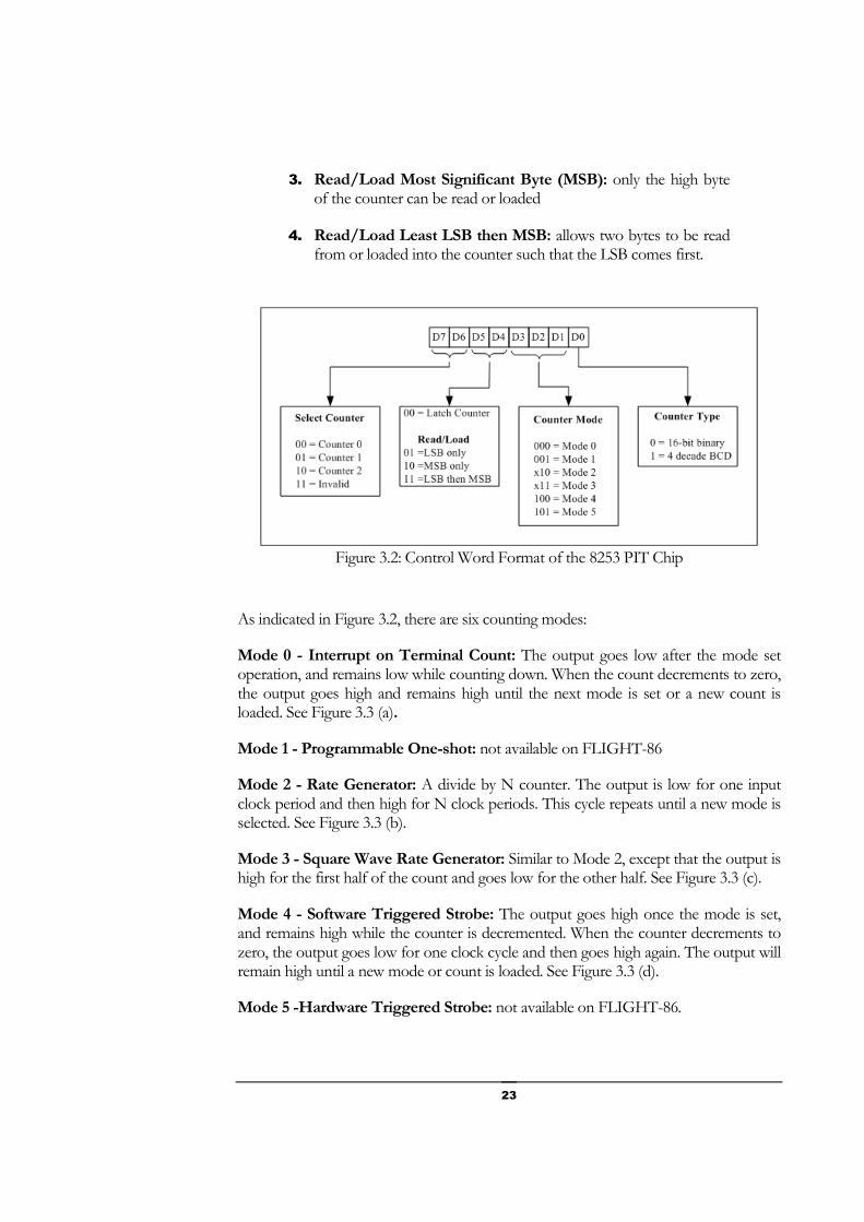
Each counter of the 8253 PIT chip can be programmed independent from the other counter by sending a control word to the Control Word Register. Figure 3.2 shows the format of the control word. Bit D0 specifies counting type (i.e. binary or BCD). Bits D3, D2, and D1 specify the counting mode. Bits D5 and D4 specify how the counter is read and loaded. Bits D7 and D6 specify the counter to be programmed (i.e. Counter 0 to Counter 2).
There are four options for reading/loading the counter:
1. Latch Counter: allows you to latch the current register count, and then read the counter value ‘on the fly’
2. Read/Load Least Significant Byte (LSB): only the low byte of the counter can be read or loaded
23
3. Read/Load Most Significant Byte (MSB): only the high byte of the counter can be read or loaded
4. Read/Load Least LSB then MSB: allows two bytes to be read from or loaded into the counter such that the LSB comes first.
Figure 3.2: Control Word Format of the 8253 PIT Chip
As indicated in Figure 3.2, there are six counting modes:
Mode 0 - Interrupt on Terminal Count: The output goes low after the mode set operation, and remains low while counting down. When the count decrements to zero, the output goes high and remains high until the next mode is set or a new count is loaded. See Figure 3.3 (a).
Mode 1 - Programmable One-shot: not available on FLIGHT-86
Mode 2 - Rate Generator: A divide by N counter. The output is low for one input clock period and then high for N clock periods. This cycle repeats until a new mode is selected. See Figure 3.3 (b).
Mode 3 - Square Wave Rate Generator: Similar to Mode 2, except that the output is high for the first half of the count and goes low for the other half. See Figure 3.3 (c).
Mode 4 - Software Triggered Strobe: The output goes high once the mode is set, and remains high while the counter is decremented. When the counter decrements to zero, the output goes low for one clock cycle and then goes high again. The output will remain high until a new mode or count is loaded. See Figure 3.3 (d).
Mode 5 -Hardware Triggered Strobe: not available on FLIGHT-86.

24
Figure 3.3: Counting modes of the 8253 PIT chip
25
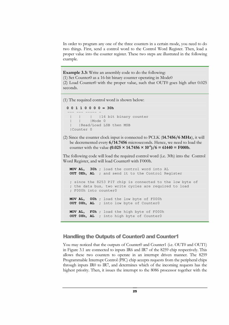
In order to program any one of the three counters in a certain mode, you need to do two things. First, send a control word to the Control Word Register. Then, load a proper value into the counter register. These two steps are illustrated in the following example.
Example 3.3: Write an assembly code to do the following: (1) Set Counter0 as a 16-bit binary counter operating in Mode0 (2) Load Counter0 with the proper value, such that OUT0 goes high after 0.025 seconds.
(1) The required control word is shown below:
0 0 1 1 0 0 0 0 = 30h --- --- ----- - | | | |16 bit binary counter | | |Mode 0 | |Read/Load LSB then MSB |Counter 0
(2) Since the counter clock input is connected to PCLK (14.7456/6 MHz), it will be decremented every 6/14.7456 microseconds. Hence, we need to load the counter with the value (0.025 × 14.7456 × 10-6)/6 = 61440 = F000h.
The following code will load the required control word (i.e. 30h) into the Control Word Register, and will load Counter0 with F000h.
MOV AL, 30h ; load the control word into AL OUT 0Eh, AL ; and send it to the Control Register ; since the 8253 PIT chip is connected to the low b yte of ; the data bus, two write cycles are required to lo ad ; F000h into counter0
MOV AL, 00h ; load the low byte of F000h OUT 08h, AL ; into low byte of Counter0 MOV AL, F0h ; load the high byte of F000h OUT 08h, AL ; into high byte of Counter0
Handling the Outputs of Counter0 and Counter1
You may noticed that the outputs of Counter0 and Counter1 (i.e. OUT0 and OUT1) in Figure 3.1 are connected to inputs IR6 and IR7 of the 8259 chip respectively. This allows these two counters to operate in an interrupt driven manner. The 8259 Programmable Interrupt Control (PIC) chip accepts requests from the peripheral chips through inputs IR0 to IR7, and determines which of the incoming requests has the highest priority. Then, it issues the interrupt to the 8086 processor together with the

26
interrupt pointer to enable the correct Interrupt Service Routine (ISR) to be executed. The 8259 PIC chip can be programmed to perform a number of modes of operation, which may be changed dynamically at any time in the program. Programming the 8253 PIC chip is not covered in this experiment. Instead, you will be given the necessary code to set the chip in a proper mode of operation.
When the output of Counter0/Counter1 goes high, it generates a request on IR6/IR7. The 8253 PIC chip handles this request as follows. If maskable interrupts are enabled by the instruction STI, the 8259 will send an interrupt to the 8086 via the INT line.
The 8086 acknowledges the interrupt request with an INTA pulse. Upon receipt of
the INTA from the 8086, the 8259 freezes the pending interrupts and waits for
another INTA pulse. When the 8086 sends the second INTA , the 8259 treats this as a Read pulse and places an 8-bit pointer onto the data bus. The pointers corresponding to requests on IR6 and IR7 are 38 and 39 respectively.
The 8086 processor uses the 8-bit pointer to fetch the address (i.e. offset and segment) of the corresponding ISR from the Interrupt Vector Table (IVT). This is done as follows. Suppose that the 8-bit pointer is n, then the 8086 will fetch four bytes starting from the address 0000:n*4. The first two bytes contain the offset of the ISR, while the next two bytes contain the segment of the ISR.
Illustrative Example
The following example illustrates how to program the 8253 PIT and 8259 PIC chips to generate time delays.
Example 3.4: Write a program to turn ON an LED for 3 seconds, then turn it OFF for another 3 seconds, and repeats this cycle. Do not use software delays.
1 2 3 4 5 6 7 8 9 10 11 12 13 14 15 16 17
COMSEG SEGMENT BYTE PUBLIC 'CODE' ASSUME CS:COMSEG, DS:COMSEG, ES:COMSEG, SS:COMSEG ORG 0100h Start: ; set the extra segment to point to the ; base of the Interrupt Vector Table (IVR) XOR AX,AX MOV ES,AX ;store the offset of ISR in the IVT MOV WORD PTR ES:[38*4],OFFSET IR6_ROUTINE ;store the segment of ISR in the IVT MOV WORD PTR ES:[38*4+2],CS ; initialize the 8255 PPI chip: ; A and C input ports, B output port MOV AL, 99h OUT 06h, AL

27
18 19 20 21 22 23 24 25 26 27 28 29 30 31 32 33 34 35 36 37 38 39 40 41 42 43 44 45 46 47 48 49 50 51 52 53 54 55 56 57
; initialize the 8259 PIC chip MOV AL, 17h OUT 10h, AL MOV AL, 20h OUT 12h, AL MOV AL, 03h OUT 12h, AL MOV AL, 3Fh OUT 12h, AL ; initialize 8253 PIT chip (00110110 = 36h) ; Counter0, load MSB then LSB, mode 3, binary MOV AL, 36h OUT 0Eh, AL ; counter loaded with F000h for 25 ms delay MOV AL, 00h OUT 08h, AL ; first load low byte MOV AL, 0F0h OUT 08h, AL ; now load high byte STI ; enable 8086 maskable interrupts MOV DL, 120 ; count for 120 interrupts (3s) ; start of main program ; switch off all LEDs MOV DH, 00h MOV AL, DH OUT 02h, AL Again: JMP Again ; wait for interrupt on IR6 ; (Counter0 decrements to 0) ; Interrupt Service Routine (ISR) for IR6 ; this routine toggles ON/OFF LED 0 every 3 seconds IR6_ROUTINE: DEC DL ; decrement interrupts counter CMP DL,0 ; if counter < 120 JNZ Return ; then exit ISR XOR DH, 01h ; else toggle LED0 MOV AL, DH OUT 02h, AL MOV DL, 120 ; count for 120 interrupts (3s) Return:IRET COMSEG ENDS END start
28
In the previous program, lines 6 and 7 set the ES segment to 0000h, which is the base address of the IVT. Lines 9 and 12 load the starting address of the ISR (IR6_ROUTINE) into the IVT. This routine will handle any request on IR6. Lines 16 and 17 initialize the 8255 PPI chip. Lines 19 to 26 initialize the 8259 PIC chip. Lines 29 and 20 initialize the 8253 PIT chip. Lines 32 to 35 load the Counter0 with the value F000h. This will generate an interrupt every 25 ms (120 interrupts every 3 seconds). The main routine starts by setting all LEDs off by sending 00h to port B (Lines 40 to 42), and waits for an interrupt on IR6 (Line 43). Upon receipt of the interrupt, the control is transferred to IR6_ROUTINE (Line 47). This routine toggles LED0 every 120 interrupts (i.e. every 3 seconds).
Exercises
3.1. Consider the following loop:
MOV CX, Y L1: DEC CX JNZ L1
What value of Y makes the loop executes in 0.225 seconds?
3.2. Modify the program in Example 3.2 such that Counter0 is set in Mode 0
3.3. Generate square waveforms with the following frequencies:
a. 100 KHz
b. 10 KHz
c. 1 KHz
3.4. Interface a simple relay driver circuit to 8255 port, and write a program switch ON/OFF a lamp every 10 seconds.
3.5. Write a program to simulate a traffic light controller (home assignment)
3.6. Write a program to simulate a lift controller (home assignment)

29
Analog to Digital & Digital
to Analog Conversion
Objective
The aim of this lab experiment is to study the Analog to Digital conversion and Digital to Analog conversion.
Equipment
Flight 8086 training board, Application board, PC with Flight86 software, download cable.
Tasks to be Performed
� Simulation of a A/D conversion employing successive approximation method using D/A converter
� Use a D/A converter to perform the following:
1. Sine wave generation (using look up table)
2. Staircase waveform generation
3. Saw-tooth waveform generation
� Read the DIL switches and output the digital values to the LEDs and DAC. The analog output of the DAC is to be represented by lighting up the bar-graph.
Experiment
4

30
4.1 Background
In any computer controlled process it may be required to monitor analog values, i.e. the output of a voltmeter or strain gauge. In order to do this, the analog signal must be first converted into a digital value using an Analog-to-Digital Converter (A/D). On the other hand, Digital-to-Analog Converters (D/A) can be used to convert a digital output from the computer into an analog value. For instance, we could generate a series of tones by changing the digital output values in such a way that the analog signal is represented as a sine wave.
4.2 A/D Conversion
The Application Board provides four sources of analog inputs which can be selected using a four position switch (SW3). The analog source can be provided externally (P2-in), or from the output of a light dependent resistor (LDR1), or from the temperature sensor (Q1), or from an on board variable voltage (UR6).
With the Application Board we can simulate a simple A/D converter that reads the output of a certain analog source (e.g. variable voltage) and converts it into a digital value as shown in Figure 4.1. By means sending values to Port-B, and hence by means of the D/A converter we can generate analog voltages proportional to the digital value we output. If this analog voltage is now compared with the unknown analog voltage, we can gradually adjust the output value to Port-A, until the comparator finds the two analog voltages equal. The digital value output to the D/A converter must be the digital value equivalent of the unknown analog input.
The output of the comparator is bit 3 of the input Port-B. A logic 1 means the output on Port-B is too small, a logic 0 means it is too large.
Figure 4.1: Simulation of an A/D Converter

31
Example 4.1: Write a program to simulate a simple A/D converter. Use the variable voltage source (UR6) as your analog source. The program should display one HEX digit (0-F) representing the digital value of the voltage input. 1 2 3 4 5 6 7 8 9 10 11 12 13 14 15 16 17 18 19 20 21 22 23 24 25 26 27 28 29 30 31 32
Set SW3 to VOLTS (Variable Voltage) Set SW4-2 to DAC (enable D/A converter) Set SW2-2, SW4-1, SW4-3, and SW4-4 OFF COMSEG SEGMENT BYTE PUBLIC 'CODE' ASSUME CS:COMSEG, DS:COMSEG, ES:COMSEG, SS:COMSEG ORG 0100h Start: MOV AL, 99h ; initialize the 8255 PPI chip OUT 06h, AL ; A input, B output, C input MOV AL, 0 ; turn off all LEDs OUT 02h, AL ANAL: MOV BL, 0 ; first digital value SMALL: MOV AL, BL ; put in AL for output OUT 02h, AL ; output value to D/A NOP ; wait for D/A NOP NOP NOP NOP NOP IN AL, 00h ; get input Port-B AND AL, 08h ; keep comparator bit (bit 3) JZ LARGE ; if value is large (bit3= 0) ; then display the digital v alue INC BL ; else increment the digital valu e JMP SMALL ; and tray again ; display the digital value as a HEX digit LARGE: MOV AL, BL CALL display_voltage JMP ANAL INCLUDE display_voltage.asm INCLUDE putc.asm COMSEG ENDS END start

32
The previous code uses two functions, namely display_voltage and putc, to display the digital value corresponding to the input voltage. The first function converts the digital (binary) value of the input voltage into an ASCII character, and calls putc to display it on the screen. The two functions are given in two separate files display_voltage.asm and putc.asm, so that you can include these two files in your code using the INCLUDE directive.
4.3 D/A Conversion
The D/A converter on the Application Board produces an analog voltage proportional to the digital input. The digital input is provided by Port-A. The analog output corresponding to 00h is 0.00V, while the analog output corresponding to the digital input FFh (255) is approximately 2.55V.
The following example shows you how to generate a SIN wave using the D/A converter.
Example 4.2: Using a set of SIN tables for data, output a sine wave in 10 degree steps, observe the analog output (at P2-Out) with an oscilloscope and measure its frequency. The first step is to construct a table containing the values of the SIN function for the following degrees: 0, 10, 20, …, 350 (see Table 4.1). Then, we assign a proper voltage to each value in the SIN table. As you know, the D/A converter can produce 256 different analog voltages (0.00V to 2.55V). Therefore, we can map a range of these voltages to the range of the SIN function (-1 to 1). Let us use the range 0.00V to 2.54V, such that 0.00V corresponds to -1 and 2.54V corresponds to 1. Since 1.27V is the mid point in the range 0.00V to 2.54V, it will be mapped to the mid point of the SIN range which is 0. Other voltage values can be mapped easily to the SIN values as shown in Table 4.1. Finally, we use the digital values corresponding to these analog voltages to generate the SIN wave as shown in the following program. 1 2 3 4 5 6
Set SW4-2 to DAC (enable D/A converter) Set SW2-1 to SWITCH Set SW4-1, SW4-3, and SW4-4 OFF COMSEG SEGMENT BYTE PUBLIC 'CODE' ASSUME CS:COMSEG, DS:COMSEG, ES:COMSEG, SS:COMSEG ORG 0100h Start: MOV AL, 99h ; initialize the 8255 PPI chip OUT 06h, AL ; A input, B output, C input

33
7 8 9 10 11 12 13 14 15 16 17 18 19 20 21 22 23 24 25 26 27 28 29 30 31 32 33 34 35 36 37 38 39 40 41 42 43 44 45 46 47 48 49 50 51 52 53 54
MOV AL, 0 ; turn off all LEDs OUT 02h, AL L1: MOV SI, OFFSET Table ; 1st element in the ta ble MOV BL, 36 ; number of elements in the table L2: LODSB ; load AL from the table OUT 02h, AL; and output the value to D/A DEC BL ; count down table JZ L2 ; loop if not zero JMP L1 ; if zero then return to the star t ; of the table Table DB 127 ; 1.27V -> sin(0) DB 149 ; 1.49V -> sin(10) DB 170 ; 1.70V -> sin(20) DB 191 ; 1.91V -> sin(30) DB 209 ; 2.09V -> sin(40) DB 224 ; 2.24V -> sin(50) DB 237 ; 2.37V -> sin(60) DB 246 ; 2.46V -> sin(70) DB 252 ; 2.52V -> sin(80) DB 254 ; 2.54V -> sin(90) DB 252 ; 1.27V -> sin(100) DB 246 ; 1.27V -> sin(110) DB 237 ; 1.27V -> sin(120) DB 224 ; 1.27V -> sin(130) DB 209 ; 1.27V -> sin(140) DB 191 ; 1.27V -> sin(150) DB 170 ; 1.27V -> sin(160) DB 149 ; 1.27V -> sin(170) DB 127 ; 1.27V -> sin(180) DB 105 ; 1.27V -> sin(190) DB 84 ; 1.27V -> sin(200) DB 64 ; 1.27V -> sin(210) DB 45 ; 1.27V -> sin(220) DB 30 ; 1.27V -> sin(230) DB 17 ; 1.27V -> sin(240) DB 8 ; 1.27V -> sin(250) DB 2 ; 1.27V -> sin(260) DB 0 ; 1.27V -> sin(270) DB 2 ; 1.27V -> sin(280) DB 8 ; 1.27V -> sin(290) DB 17 ; 1.27V -> sin(300) DB 30 ; 1.27V -> sin(310) DB 45 ; 1.27V -> sin(320) DB 64 ; 1.27V -> sin(330) DB 84 ; 1.27V -> sin(340) DB 105 ; 1.27V -> sin(350) COMSEG ENDS END start
34
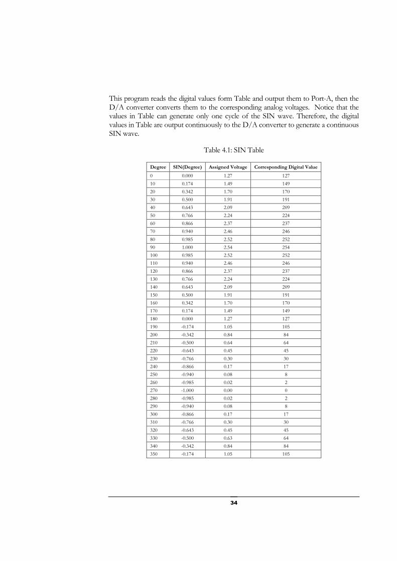
This program reads the digital values form Table and output them to Port-A, then the D/A converter converts them to the corresponding analog voltages. Notice that the values in Table can generate only one cycle of the SIN wave. Therefore, the digital values in Table are output continuously to the D/A converter to generate a continuous SIN wave.
Table 4.1: SIN Table
Degree SIN(Degree) Assigned Voltage Corresponding Digital Value
0 0.000 1.27 127
10 0.174 1.49 149
20 0.342 1.70 170
30 0.500 1.91 191
40 0.643 2.09 209
50 0.766 2.24 224
60 0.866 2.37 237
70 0.940 2.46 246
80 0.985 2.52 252
90 1.000 2.54 254
100 0.985 2.52 252
110 0.940 2.46 246
120 0.866 2.37 237
130 0.766 2.24 224
140 0.643 2.09 209
150 0.500 1.91 191
160 0.342 1.70 170
170 0.174 1.49 149
180 0.000 1.27 127
190 -0.174 1.05 105
200 -0.342 0.84 84
210 -0.500 0.64 64
220 -0.643 0.45 45
230 -0.766 0.30 30
240 -0.866 0.17 17
250 -0.940 0.08 8
260 -0.985 0.02 2
270 -1.000 0.00 0
280 -0.985 0.02 2
290 -0.940 0.08 8
300 -0.866 0.17 17
310 -0.766 0.30 30
320 -0.643 0.45 45
330 -0.500 0.63 64
340 -0.342 0.84 84
350 -0.174 1.05 105
35
Exercises
6.1. Consider Example 4.1. Describe how you would minimize the number of digital values required to find the unknown voltage.
6.2. How could you vary the frequency of the SIN wave generated in Example4.2?
6.3. Use the D/A converter to perform the following:
a. Staircase waveform generation
b. Saw-tooth waveform generation
6.4. The bar-graph (U10) is essentially a bank of 10 LEDs. It is driven by U11 (LM3914) which samples a voltage input signal, as the signal exceeds certain preset levels it will output a signal to light one of the LEDs on the bar-graph. Hence, as the voltage increases, more LEDs will be turned on.
a. Write a program to read the DIL switches and output the digital values to the LEDs and DAC. The analog output of the DAC is to be represented by lighting up the bar-graph.
b. Plot a graph of switch digital value against the number of LEDs alight on the bar-graph.

36
Controlling DC Motors
Objective
The aim of this lab experiment is to control a small DC motor.
Equipment
Flight 8086 training board, Application board, PC with Flight86 software, download cable
Tasks to be Performed
� Running the motor in forward and reverse direction for a specified time
� Controlling the speed of the motor
Experiment
5

37
5.1 DC Motor
The Application Board contains a small DC motor that can be operated in the forward or reverse direction. The operation of this DC motor is controlled by bits 6 and 7 on Port-A as shown in Table 5.1.
Table 5.1: Operation Modes of the DC Motor
Bit6 Bit7 Operation 0 0 0 1 1 0 1 1
Stop Reverse Direction Forward Direction
Stop
The following example shows you how to run the DC motor in the forward and reverse direction for a specific time.
Example 4.1: Write a program to run the DC motor in the forward direction for 5 seconds, turn it off for 3 seconds, then run it in the revere direction for 5 seconds.
Set SW2-1 to SWITCH Set SW2-2 to MOTOR SW4-1, SW4-2, SW4-3, and SW4-4 OFF MOV AL, 99h ; initialize the 8255 PPI chip OUT 06h, AL ; A input, B output, C input MOV DL, ? ; load a proper value for 5s delay MOV AL, 40h ; forward direction OUT 02h, AL CALL Delay MOV DL, ? ; load a proper value for 3s delay MOV AL, 00h ; stop the motor OUT 02h, AL CALL Delay MOV DL, ? ; load a proper value for 5s delay MOV AL, 80h ; reverse direction OUT 02h, AL CALL Delay MOV AL, 00h ; stop the motor OUT 02h, AL INT 5 ; the delay procedure is left as an exercise

38
5.3 Controlling the Speed of the DC Motor
When the DC motor is ON (forward/reverse), it operates in its maximum speed. However, the speed of the motor can be controlled using pulse width modulation (PWM).
PWM is a common technique for speed control. A good analogy is bicycle riding. You peddle (exert energy) and then coast (relax) using your momentum to carry you forward. As you slow down (due to wind resistance, friction, road shape) you peddle to speed up and then coast again. The duty cycle is the ratio of peddling time to the total time (peddle+coast time). A 100% duty cycle means you are peddling all the time, and 50% only half the time.
PWM for motor speed control works in a very similar way. Instead of peddling, your motor is given a fixed voltage value (turned on) and starts spinning. The voltage is then removed (turned off) and the motor "coasts". By continuing this voltage on-off duty cycle, motor speed is controlled.
The concept of PWM inherently requires timing. The 8253 PIT chip can be used to generate PWM. In the beginning, the motor is turned on and Counter 0 is loaded with the ON duration. When Counter 0 terminates, the motor is turned off and Counter 1 is loaded with the OFF duration. Now, when Counter 1 terminates, the process is repeated from the beginning.
Example 4.2: Write a program to control the speed of the DC motor based on the state of Bit0 of the DIP switch. If Bit0 = 0, the motor will run at maximum speed. Otherwise, it will run at 50% of its duty cycle.
1 2 3 4 5 6 7 8 9 10 11 12 13 14 15
Set SW2-1 to SWITCH Set SW2-2 to MOTOR SW4-1, SW4-2, SW4-3, and SW4-4 OFF COMSEG SEGMENT BYTE PUBLIC 'CODE' ASSUME CS:COMSEG, DS:COMSEG, ES:COMSEG, SS:COMSEG ORG 0100h Start: ; set the external segment to point to the ; base of the Interrupt Vector Table (IVR) XOR AX,AX MOV ES,AX ;store the offset of ISR in the IVT MOV WORD PTR ES:[38*4],OFFSET IR6_ROUTINE ;store the segment of ISR in the IVT MOV WORD PTR ES:[38*4+2],CS ;store the offset of ISR in the IVT MOV WORD PTR ES:[39*4],OFFSET IR7_ROUTINE ;store the segment of ISR in the IVT MOV WORD PTR ES:[39*4+2],CS

39
16 17 18 19 20 21 22 23 24 25 26 27 28 29 30 31 32 33 34 35 36 37 38 39 40 41 42 43 44 45 46 47 48 49 50 51 52 53 54 55 56 57 58 59 60 61
; initialize the 8255 PPI chip: ; A and C input ports, B output port MOV AL, 99h OUT 06h, AL ; initialize the 8259 PIC chip MOV AL, 17h OUT 10h, AL MOV AL, 20h OUT 12h, AL MOV AL, 03h OUT 12h, AL MOV AL, 3Fh OUT 12h, AL ; initialize 8253 PIT chip (00110000 = 30h) ; Counter0, load MSB then LSB, mode 0, binar y MOV AL, 30h OUT 0Eh, AL ; initialize 8253 PIT chip (01110000 = 70h) ; Counter1, load MSB then LSB, mode 0, binar y MOV AL, 70h OUT 0Eh, AL ; counter0 loaded with FFFFh MOV AL, 0FFh OUT 08h, AL ; first load low byte MOV AL, 0FFh OUT 08h, AL ; now load high byte STI ; enable 8086 maskable interrupts ; start of main program MOV AL, 40h ; turn on the motor OUT 02h, AL again: JMP again ; wait for interrupt on IR6/IR7 ; Counter0/Counter1 decrements t o 0 ; Interrupt Service Routine (ISR) for IR6 ; this routine checks Bit0 of the DIP switch ; If Bit0 = 0 continue running the motor (max speed ) ; If Bit0 = 1 stop the motor (50% duty cycle) ; the routine also reload Counter 1 IR6_ROUTINE: IN AL, 00h ; read DIP switch TEST AL, 01h ; check Bit0 JZ continue ; if Bit0=0 then don't stop the m otor MOV AL, 00h ; else stop the motor OUT 02h, AL continue: ; counter1 loaded with FFFFh (50% duty cycle) MOV AL, 0FFh
40
70 71 72 73 74 75 76 78 79 80 81 82 83 84 85 86 87 88
OUT 0Ah, AL ; first load low byte MOV AL, 0FFh OUT 0Ah, AL ; now load high byte IRET ; Interrupt Service Routine (ISR) for IR7 ; this routine turn on the motor and reload Counter 0 IR7_ROUTINE: MOV AL, 40h ; turn on the motor OUT 02h, AL ; counter0 loaded with FFFFh MOV AL, 0FFh OUT 08h, AL ; first load low byte MOV AL, 0FFh OUT 08h, AL ; now load high byte IRET COMSEG ENDS END start
Exercises
5.1. Modify Example 5.2 to allow the user to control the direction in addition to the speed (Use Bit1 to control the direction).
5.2. Modify Example 5.2 to operate the motor at 4 different, for example 100% duty cycle, 50% duty cycle, 25% duty cycle, and 5 % duty cycle. The speed is selected based on the states of Bit0 and Bit1.

41
Interfacing a Hyper
Terminal to the Flight 86
Kit
Objective
The aim of this lab experiment is to interface a Hyper Terminal to 8086 processor by programming the 8251 USART.
Equipment
� Flight 8086 training board,
� PC with Flight86 software, and
� Download cable
Tasks to be Performed
Reading data from the keyboard and displaying it on the Hyper Terminal using RS-232 standard interface and asynchronous serial communication
Experiment
6

42
6.1 Background
The Intel 8251 Universal Synchronous/Asynchronous Receiver/Transmitter (USART), designed for data communication with Intel's microprocessor families. It is used as a peripheral device and is programmed by the CPU to operate using many serial data transmission techniques.
The USART accepts data characters from the CPU in parallel format and then converts them into a continuous serial data stream. It accepts serial data streams and converts them into parallel data characters for the CPU. The USART will signal the CPU whenever it can accept a new character for transmission or whenever it has received a character for the CPU. The CPU can read the status of the USART at any time. The status includes data transmission errors and control signals.
Although the USART is capable of operating in synchronous and asynchronous modes, it is probable that most work will be carried out in the asynchronous mode. Therefore, asynchronous operation only will be described in this experiment.
The 8251 USART chip may operate its transmitter and receiver independently. It may even operate them at different speeds. However, on the FLIGHT-86 board, they both work at the same speed which can be programmed using Counter 2 of the 8253 PIT chip.
Registers
The 8251 USART chip has four register:
1. The Data Register is used to store recently received data byte or the data byte that is ready to be transmitted.
2. The Mode Register is used to set the operation mode of the 8251 chip.
3. The Control Register is used to send commands to the 8251 chip.
4. The Status Register reflects the current status of 8251 chip.
Table 6.1 shows the actual port addresses and allowed activities of these four registers in the FLIGHT-86 board.

43
Table 6.1: The 8251 Registers
Register Activity Allowed Actual Port Address Data Mode Control Status
Read/Write Write Only Write Only Read Only
18h 1Ah 1Ah 1Ah
Control Words
The 8251 USART chip can be programmed using two types of control words:
(1) The Mode Instruction, which must follow a reset (internal or external) to specify the general operation of the chip. This control word can be sent through the MODE register according to the format shown in Figure 6.1 (a). The baud rate of the transmitter/receiver depends on the frequency of the input clock of the transmitter/receiver. For example, if the input clock runs at 9600Hz (i.e. 9600 cycles per second), then the 8251 can transmit/receive 9600 bits per second (i.e. 1 bit every clock cycle). The baud rate factor is used to adjust the baud rate by a certain factor (i.e. divide the baud rate by 1, 16 or 64).
(2) The Command Instruction, which defines the detailed operation. Command instructions can by sent after a mode instruction using the COMMAND register according to the format shown in Figure 6.1 (b). All command instructions must keep D6 zero. Setting this bit to 1 will reset the USART and make it ready to accept a new mode word.
Status Word
The CPU can examine the STATUS register at any time to determine the current condition of the 8251. The format of the 8251 status word is given in Table 6.2.
Sending Data
Provided the transmitter is enabled, as soon as a data byte is written to the DATA register, the 8251 will convert this to a serial form and send it to the serial output pin in the format specified. If the receiving device is not ready the data byte will be held and sent as soon as possible.
Sending Data
Provided that the receiver is enabled, the 8251 will receive a serial data byte sent to it from another device, and will store it in the DATA register. The CPU can identify if a character has been received (e.g. by checking the STATUS register) and read the data byte form the DATA register. Once the data byte is read the DATA register is flushed.

44
Figure 6.1: 8251 Control Words
Table 6.1: 8251 Status Word
BIT Description 0 Transmitter
Ready This bit is set when the transmitter is ready to receive a new character for transmission from the CPU.
1 Receiver Buffer Full
This bit s set when a character is received on the serial input.
2 Transmitter Buffer Empty
This bit is set as soon as the USART completes transmitting a character and a new one has not been loaded in time. It goes low only while a data character is being transmitted by the USART.
3 Parity Error This bit is set when parity is enabled and a parity error is detected in any received character.
4 Overrun Error This bit is set when the CPU does not read a received character before the next one becomes available. However, the previous character is lost.
5 Framing Error This bit is set when a valid stop bit (high) is not detected at the end of a received character.
6 Synchronous Detect/ Break Detect
Used for synchronous mode only
7 Data Set Ready This is a general-purpose input bit that can be read by the CPU as part of the 8251status.

45
6.2 Programming the 8251 USART Chip
In order to program the 8251 USART chip in asynchronous mode, you need to do the following:
1. Set the receiver/transmitter input clock to the desired baud rate. In the FLIGHT-86, this is done by programming Counter 2 of the 8253 PIT chip.
2. Send asynchronous mode instruction with the desired format.
3. Send a command instruction to enable the transmitter/receiver.
Setting up the Baud Rate
Since the output of Counter 2 is connected to the input clocks of the transmitter and receiver, Counter 2 can be used to control the speed (baud rate) of transmission/reception. If we program Counter 2 in mode 3 and load it with some number N, then the transmitter/receiver can be operated at 14.7456/(N×6) MHz. In other words, the transmitter/receiver can transmit/receive 14.7456×10⁶/(N×6) bits per second. For instance, to get a baud rate of 9600, we need to load Counter 2 with 14.7456×10⁶/(9600×6) = 256.
Sending a Mode Instruction
After a system RESET the MODE register must be the first to be set. Because the 8251 may be in an unknown state, it is normal practice to send the byte 00h to the COMMAND register three times. This will guarantee the 8251 COMMAND register is active. Now, the byte value 40h (D6 is 1) is sent to activate the MODE register. The desired asynchronous format may now be set up and sent to the MODE register.
Sending a Control Instruction
Once the mode has been programmed the 8251 will switch to the COMMAND register. Now, you can send a command instruction according to the format shown in Figure 6.1 (b) to enable the transmitter or the receiver or both.

46
Example 4.1: Write a program that continuously reads one character from the keyboard and displays it on the Hyper Terminal.
1 2 3 4 4 5 6 7 8 9 10 11 12 13 14 15 16 17 18 19 20 21 22 23 24 25 26 27 28 29 30 31 32 33 34 35 36 37 38 39 40 41 42 43 44
COMSEG SEGMENT BYTE PUBLIC 'CODE' ASSUME CS:COMSEG, DS:COMSEG, ES:COMSEG, SS:COMSEG ORG 0100H Start: ; send 00h three times to ensure that ; the command register is active MOV AL, 00h CALL Send_Control_Word CALL Send_Control_Word CALL Send_Control_Word ; send 40h to activate the mode register ; (D6=1 internal reset) MOV AL, 40h CALL Send_Control_Word ; send a mode instruction, namely ; 0100 1101 = 4Dh ; baud factor=1, 8-bit char, no parity, 1 sto p bit MOV AL, 4Dh ;mode register 0100 1110 CALL Send_Control_Word ; send a command instruction to enable ; both the transmitter and receiver MOV AL, 37h CALL Send_Control_Word ; initialize 8253 PIT chip (1011 0110 = B6h) ; Counter2, load MSB then LSB, mode 3, binary MOV AL, 0B6h OUT 0Eh, AL ; counter loaded with 0100h (baud rate = 9600) MOV AL, 00h OUT 0Ch, AL ; first load low byte MOV AL, 01h OUT 0Ch, AL ; now load high byte L1: IN AL, 1Ah; read status word TEST AL, 02h; check receiver buffer JZ L1 ; if buffer is empty then try again IN AL, 18h ; else get the character in the buffer OUT 18h, AL ; and output it to the Hyper Terminal JMP L1 ; repeat the process Send_Control_Word: OUT 1Ah, AL ; send the control word MOV CX, 200h ; delay to ensure 8251 catches up Delay: LOOP Delay RET COMSEG ENDS END start

47
Note that once you run the program of Example 6.1 on the FLIGHT-86, you need to close the F86GO program to allow the Hyper Terminal to communicate with the program through the serial cable. This is because the serial communication port may not be used by more than one application at the same time.
Exercises
6.1. Write a program to read a string from the keyboard and display it on the Hyper Terminal in a reverse order.
6.2. Write a program to read a decimal number (between 0 and 255) from the keyboard and display it on the Hyper Terminal as a binary number.

48
Mini Project
In this part, students will be carrying out a mini project of designing an interface board for certain application. This mini project will be carried out in groups. The students will use PCB design tools for entering schematic and generating layout
for fabrication of the interface card. The interface board will need to be interfaced to their fabricated processor board. They are required to select an appropriate peripheral chip depending upon the application chosen and design the complete circuit and develop the control software to perform the required task.
Some of the mini projects that can be offered to the students are:
� Interfacing Keyboard (either PC keyboard or Keypad matrix) � Interfacing CRT monitor � Interfacing LED matrix character Display or LCD display ( to display
alphanumeric messages) � Interfacing 7-segment LEDs ( to display address and data appearing
on the system bus, contents of the internal registers) � Traffic Light controller � Lift controller � Smart Card Reader � Stepper motor control ( robotic arm control application) � Data Acquisition system ( using A/D and D/A converters) � Serial I/O communication between processor kits ( file transfer ) � Printer Interface (printers using Centronics parallel Interface) � Simple IC tester � Voting machine � Quiz/JAM key/buzzer and scoreboard control � Counting Application (example, to count the number of visitors
entering an Exhibition Hall)
Part
2
I

49
Appendices
� 8086 Microprocessor
� 8284 Clock Generator
� TTL Data Sheets
� 8255 Programmable Peripheral Interface (PPI)
� 8253 Programmable Interval Timer (PIT)
� 8259 Programmable Interrupt Controller (PIC)
� 8251 Universal Synchronous Asynchronous Receiver Transmitter (USART)

50