MICROPROCESSOR TECHNOLOGY - Academic Site · MICROPROCESSOR TECHNOLOGY Assis. Prof. ... The block...
29
21-Apr-15 1 MICROPROCESSOR TECHNOLOGY Assis. Prof. Hossam El-Din Moustafa Lecture 13 Ch.6 The 80186, 80188, and 80286 Microprocessors
Transcript of MICROPROCESSOR TECHNOLOGY - Academic Site · MICROPROCESSOR TECHNOLOGY Assis. Prof. ... The block...
21-Apr-15 1
MICROPROCESSOR TECHNOLOGY
Assis. Prof. Hossam El-Din Moustafa
Lecture 13
Ch.6 The 80186, 80188, and 80286 Microprocessors
21-Apr-15 2
Chapter Objectives
Describe the hardware and software enhancements of the 80186/80188 and the 80286 microprocessors.
Detail the differences between the various versions of the 80186 and 80188 controllers.
Describe the memory and I/O interface.
Describe the operation of the memory management unit (MMU) in the 80286 µP.
Define the operation of the Real-Time Operating System (RTOS).
21-Apr-15 3
80186/80188 Architecture
The 80186 contains 16-bit data bus.
The 80188 contains 8-bit data bus.
The 80186/80188 contain additional reserve interrupt vectors and some powerful built-in I/O features.
The 80186/80188 are called embedded controllers as they are used as controllers not as a microprocessor-based computer.
IOM /
21-Apr-15 4
80186/80188 Basic Block Diagram
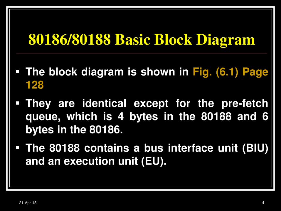
The block diagram is shown in Fig. (6.1) Page 128
They are identical except for the pre-fetch queue, which is 4 bytes in the 80188 and 6 bytes in the 80186.
The 80188 contains a bus interface unit (BIU) and an execution unit (EU).
21-Apr-15 5
80186/80188 Basic Block Diagram
The family contains a clock generator, a programmable interrupt controller, programmable timers, a programmable DMA controller, and a programmable chip selection unit.
The 80186/80188 can be used as caching disk controllers, LAN controllers, and in the cellular telephone network as switchers.
21-Apr-15 6
80186/80188 Basic Features
1. Clock Generator: Internal (instead of the external 8284A)
It has three pins; X1, X2, and CLKOUT
X1 and X2 are connected to a crystal that resonates at twice the operating frequency of the µP.
The 80186/80188 is available in 6 MHz, 8 MHz, 12 MHz, 16 MHz, and 25 MHz.
The CLKOUT provides a system clock signal that is ½ the crystal frequency with 50% duty cycle.
The clock generator provides the internal timing for synchronizing the READY input pin.
21-Apr-15 7
80186/80188 Basic Features
2. Programmable Interrupt Controller (PIC)
It arbitrates the internal and external interrupts and controls up to 2 external 8259 PICs.
It has 5 interrupt inputs; INT0 INT3 and NMI
3. Programmable DMA Unit
It contains 2 DMA channels.
Each channel can transfer data between memory locations, between memory and I/O, or between I/O devices.

21-Apr-15 8
80186/80188 Basic Features
4. Timers
The timer section contains 3 fully programmable 16-bit timers.
Timers 0, 1 generate waveforms for external use or to count external events.
Timer 2 is internal, clocked by the master clock.
Timer 2 generates an interrupt after a specified number of clocks and can provide a clock to the other timers.
21-Apr-15 9
80186/80188 Basic Features
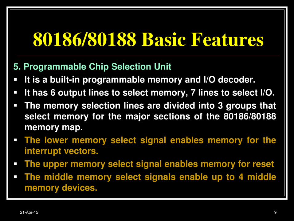
5. Programmable Chip Selection Unit
It is a built-in programmable memory and I/O decoder.
It has 6 output lines to select memory, 7 lines to select I/O.
The memory selection lines are divided into 3 groups that select memory for the major sections of the 80186/80188 memory map.
The lower memory select signal enables memory for the interrupt vectors.
The upper memory select signal enables memory for reset
The middle memory select signals enable up to 4 middle memory devices.
21-Apr-15 10
80186/80188 Basic Features
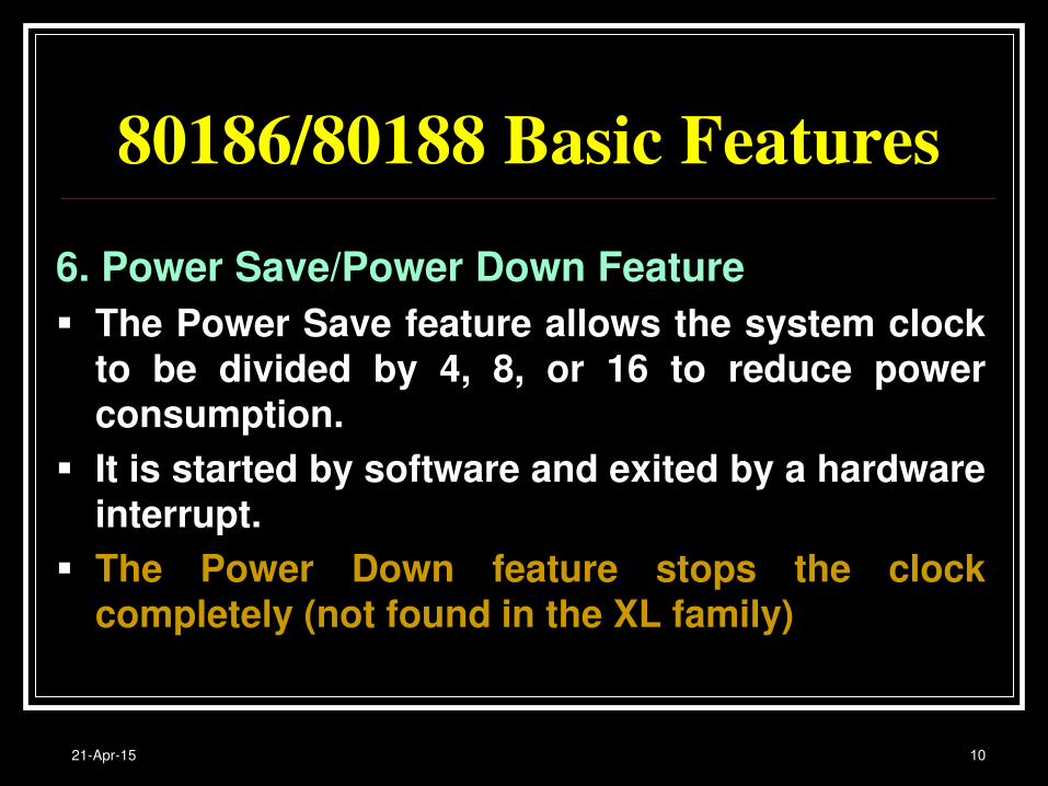
6. Power Save/Power Down Feature
The Power Save feature allows the system clock to be divided by 4, 8, or 16 to reduce power consumption.
It is started by software and exited by a hardware interrupt.
The Power Down feature stops the clock completely (not found in the XL family)

21-Apr-15 11
80186/80188 Basic Features
7. Refresh Control Unit
It generates the refresh row address at the interval programmed.
The refresh address is provided to the memory system at the end of the programmed refresh interval along with the RFSH control signal.
21-Apr-15 12
80186/80188 Pin-Out
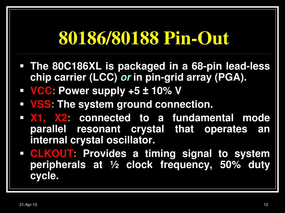
The 80C186XL is packaged in a 68-pin lead-less chip carrier (LCC) or in pin-grid array (PGA).
VCC: Power supply +5 ± 10% V
VSS: The system ground connection.
X1, X2: connected to a fundamental mode parallel resonant crystal that operates an internal crystal oscillator.
CLKOUT: Provides a timing signal to system peripherals at ½ clock frequency, 50% duty cycle.

21-Apr-15 13
80186/80188 Pin-Out
RES: Resets the µP. It must be held low for at least 50 ms after power is applied.
RESET: Rest output pin goes high when RES is low.
TEST: Connects to the BUSY output of the 80187 coprocessor.
TMRIN0, TMRIN1: external clocking resources to timers 0, 1.
TMROUT0, TMROUT1: provide the output signals from timers 0, 1

21-Apr-15 14
80186/80188 Pin-Out
DRQ0, DRQ1: Active high level triggered DMA request lines for DMA channels 0, 1.
NMI: Non-maskable interrupt which, when active, uses interrupt vector 2.
INT0, INT1, INT2/INTA0, INT3/INTA1: Maskable interrupt inputs which are configured as 4 interrupt inputs if no external 8259 is present, or as two interrupt inputs if 8259s are present.
21-Apr-15 15
80186/80188 Pin-Out
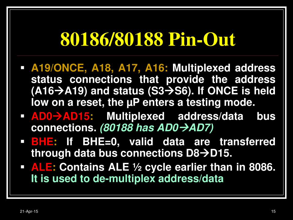
A19/ONCE, A18, A17, A16: Multiplexed address status connections that provide the address (A16A19) and status (S3S6). If ONCE is held low on a reset, the µP enters a testing mode.
AD0AD15: Multiplexed address/data bus connections. (80188 has AD0AD7)
BHE: If BHE=0, valid data are transferred through data bus connections D8D15.
ALE: Contains ALE ½ cycle earlier than in 8086. It is used to de-multiplex address/data
21-Apr-15 16
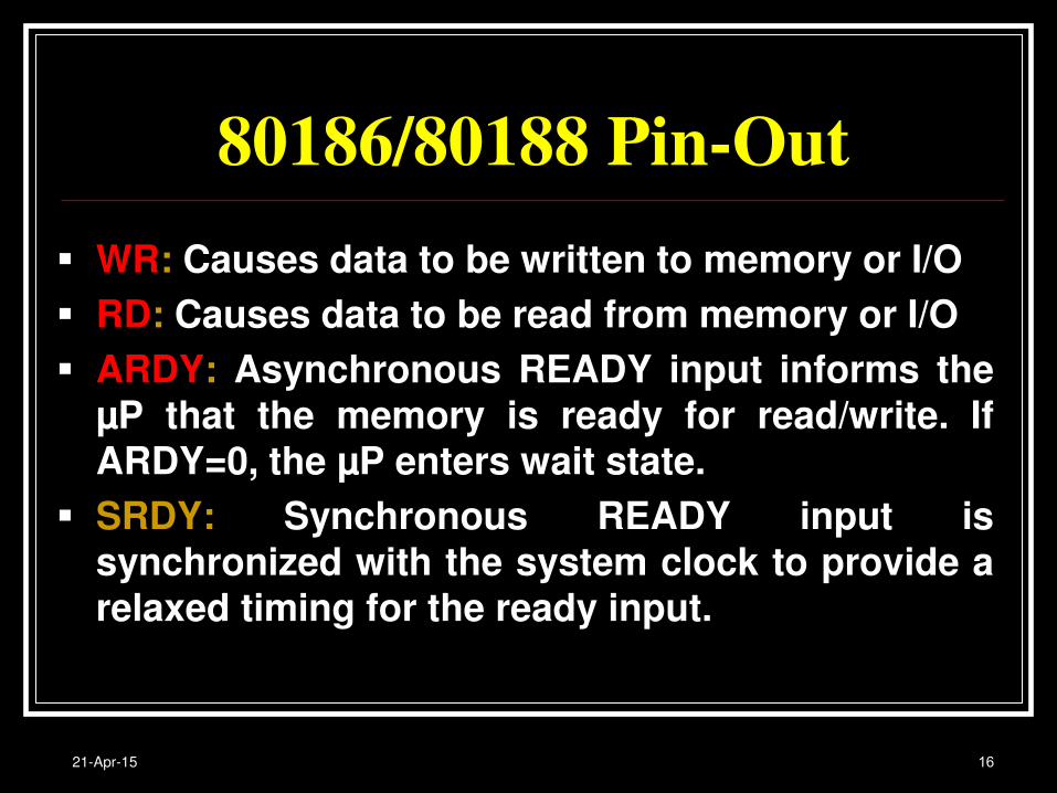
80186/80188 Pin-Out
WR: Causes data to be written to memory or I/O
RD: Causes data to be read from memory or I/O
ARDY: Asynchronous READY input informs the µP that the memory is ready for read/write. If ARDY=0, the µP enters wait state.
SRDY: Synchronous READY input is synchronized with the system clock to provide a relaxed timing for the ready input.

21-Apr-15 17
80186/80188 Pin-Out
LOCK: It is controlled by the LOCK prefix.
S0, S1, S2: Status bits that provide the system with the type of bus transfer in effect.
UCS: Upper Memory Chip Select pin selects memory on the upper portion of the memory map (ending at FFFFF).
LCS: Lower Memory Chip Select pin selects memory on the lower portion of the memory map (Starting at 00000).
21-Apr-15 18
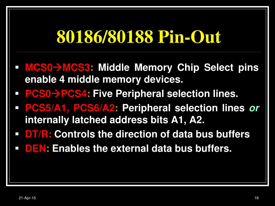
80186/80188 Pin-Out
MCS0MCS3: Middle Memory Chip Select pins enable 4 middle memory devices.
PCS0PCS4: Five Peripheral selection lines.
PCS5/A1, PCS6/A2: Peripheral selection lines or internally latched address bits A1, A2.
DT/R: Controls the direction of data bus buffers
DEN: Enables the external data bus buffers.

21-Apr-15 19
DC Operating Characteristics
+5V ± 10% V
Between 42-63 mA of power supply current
Each o/p pin provides 3mA of logic 0 current and -2mA of logic 1 current.
Timing:
Four clocking periods = one bus cycle
The 16 MHz version requires a ….. ns bus cycle? complete

21-Apr-15 20
Programming The 80186/80188 Enhancements
1. Peripheral Control Block:
All internal peripherals are controlled by a set of 16-bit wide registers located in the peripheral control block (PCB). See Fig. P 136
The PCB is a set of 256 registers located in the I/O or memory space.
Whenever the processor is reset, the PCB is automatically located at the top of the I/O map.
Relocation is accomplished by changing the contents of the relocation register (see Fig. P. 137).
21-Apr-15 21
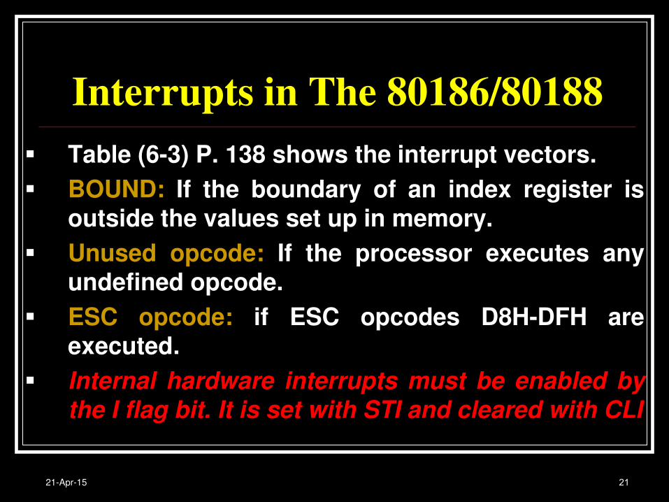
Interrupts in The 80186/80188
Table (6-3) P. 138 shows the interrupt vectors.
BOUND: If the boundary of an index register is outside the values set up in memory.
Unused opcode: If the processor executes any undefined opcode.
ESC opcode: if ESC opcodes D8H-DFH are executed.
Internal hardware interrupts must be enabled by the I flag bit. It is set with STI and cleared with CLI
21-Apr-15 22
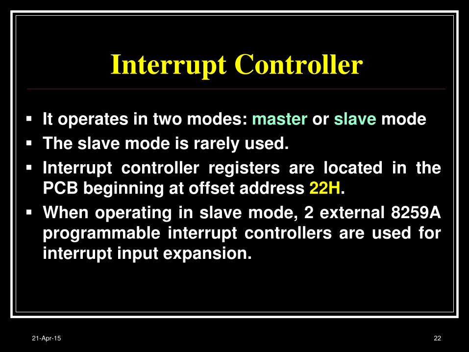
Interrupt Controller
It operates in two modes: master or slave mode
The slave mode is rarely used.
Interrupt controller registers are located in the PCB beginning at offset address 22H.
When operating in slave mode, 2 external 8259A programmable interrupt controllers are used for interrupt input expansion.

21-Apr-15 23
Interrupt Controller
Interrupt Control registers: Each interrupt
control register controls a single interrupt source
The mask bit enables (0) or disables (1) the interrupt input represented by the control word.
The priority bits set the priority level of the interrupt source. (highest 000, lowest 111)
The CAS bit enables slave mode (CAS=0)
The SFNM bit selects the special fully nested mode. (Fig. 6-11 Page 141)
21-Apr-15 24
Interrupt Controller
Interrupt Request Register:
It contains an image of the interrupt sources in each mode of operation.
Whenever an interrupt is requested, the corresponding interrupt request bit becomes a logic 1.

21-Apr-15 25
Interrupt Controller
Mask and Priority Mask Registers: If a source is masked (disabled), the
corresponding bit of the interrupt mask register contains a logic 1.
The interrupt mask register is read to determine which interrupt sources are masked and which are enabled.
The priority mask register shows the priority of the interrupt currently being serviced.
21-Apr-15 26
Interrupt Controller
In-Service Register
The bit that corresponds to the interrupt source is set if the µP is currently acknowledging the interrupt.
The bit is reset at the end of an interrupt.
21-Apr-15 27
Interrupt Controller
The Poll and Poll Status Register It has a bit (IREQ) that indicates an interrupt is
pending.
This bit is set if an interrupt is received with sufficient priority and cleared when an interrupt is acknowledged.
The S bits indicate the interrupt vector type number of the highest priority pending interrupt.
They are used in master mode not in slave mode

21-Apr-15 28
Interrupt Controller
End-of-Interrupt Register (EOI):
It causes the termination of an interrupt when written by a program.
Interrupt Status Register:
T0T2 indicate which timer is causing an interrupt
The DHLT bit is only used in master mode. When set, it stops a DMA action.
Interrupt Vector Register:
It is present in the slave mode. It is used to specify the most significant 5 bits of the interrupt vector type number

21-Apr-15 29
Thank You
With all best wishes !!