Micro-Raman study of stress distribution in local ...
9
Micro-Raman study of stress distribution in local isolation structures and correlation with transmission electron microscopy I. De Wolf, J. Vanhellemont, A. Romano-Rodrfgueza) H. NorstrOm b, and H. Interuniversity Micro-Electronics Center (IMEC), Kapeldreef 75, B-3001 Leuvh, Belgium E. Maes (Received 31 July 1991; accepted for publication 7 October 1991) Stress in local isolation structures is studied by micro-Raman spectroscopy. The results are correlated with predictions of an analytical model for the stress distribution and with cross-sectional transmission electron microscopy observations. The measurements are performed on structures on which the S&N4 oxidation mask is still present. The influence of the pitch of the periodic local isolation pattern, consisting of parallel lines, the thickness of the mask, and the length of the bird’s beak on the stress distribution are studied. It is found that compressive stress is present in the Si substrate under the center of the oxidation mask lines, with a magnitude dependent on the width of the lines. Large tensile stress is concentrated under the bird’s beak and is found to increase with decreasing length of the bird’s beak and with increasing, thickness of the S&N4 film. I. INTRODUCTION II. EXPERIMENT During the last years, micro-Raman spectroscopy has been used increasingly as a powerful technique to measure local residual stress in submicrometer isolation devices, e.g., in local oxidation of silicon (LOCOS) structures,1-3 isolation trenches,4 and V-groove structures.5 Processing of such nonplanar structures introduces large local stress, es- pecially at discontinuities of the different film layers. Such localized stresses can induce various types of structural defects that degrade the circuit performance. The conven- tional LOCOS technique has been extensively employed as an isolation technique in very large-scale integration (VLSI) devices because of its simplicity. This technique is based on a selective oxidation process using silicon nitride as a mask against oxidation of the active device regions. A drawback is the diffusion of oxygen through the pad oxide during field oxidation, causing additional oxide growth un- der the edge of the nitride mask, giving rise to the forma- tion of a so-called “bird’s beak” (BB). This unwanted ef- fect limits the available active surface area and, thus, the packing density. To reduce the size of the bird’s beak, mod- ified LOCOS techniques are explored with the local oxida- tion of’polysilicon over silicon (LOPOS) technique as one of the most promising approaches. In this technique a poly-Si layer is deposited between the pad oxide and a relative thick nitride mask. The lateral diffusion of the ox- ide under the nitride mask is thus reduced and part of the stress induced in the silicon by the nitride mask is com- pensated by the poly layer. Shortening the BB leads, how- ever, to a strong increase of the local stress in the silicon substrate. This stress is studied with micro-Raman spec- troscopy and the results are compared with cross-sectional transmission electron microscopy (XTEM) and with the predictions of a simple planar stress model. The isolation structures are fabricated on (00 1) silicon substrates. Experiments are performed on three different LOPOS structures and one LOCOS structure. The process parameters of the different samples are listed in Table I. In all samples a pad oxide is grown by dry oxidation. In LO- POS this is followed by deposition of poly-amorphous sil- icon. Next a low-pressure chemical-vapor deposition (LPCVD) S&N4 film is deposited and patterned using pho- tolithography, resulting in long, [ 1 IO]-oriented, Si3N4 lines with different widths. Finally a field oxide is grown by wet oxidation at different temperatures and for different oxida- tion times. Raman spectra are measured in backscattering config- uration using the 48&O- or 457.9~nm line of an argon laser with output power of maximal 30 mW. The 457.9-nm line is used in most experiments because of its short penetration depth in c-Si, so that only the top layer of the silicon sub- strate, where stress is expected to be largest, is probed during the Raman experiments. The incoming light is po- larized along the length of the lines, the scattered light is, in most experiments, not analyzed. The diameter of the probed region is smaller than 1 pm. The sample is moved with an X-Y translation stage in steps of minimum 0.1 ,!.cm and at each position single-point Raman spectra are re- corded. In this way the spatial variation of the Raman signal over the structures on the silicon surface is obtained. In all samples the central line of a series of five parallel lines is scanned. The spacing between these lines is equal to their width. The Raman spectra are fitted with a Lorent- zian function, reducing the error on the peak position es- timation to values smaller than 0.05 cm -- I. Laser plasma lines are used for internal calibration. Ill. THiORY B’Present address: LCMM, Departament de Fisica Aplicada i Electrbnica, University of Barcelona, Diagonal 645, E-08028 Barcelona, Spain. “Present address: Swedish Institute of Micro-Electronics, P.O. Box 1084, S-16421 Kista, Sweden. A. Raman spectroscopy Crystalline silicon (c-Si) has three active optical vibra- tions: two transversal (TO1 and TOz) along x = {loo] and 898 J. Appl. Phys. 71 (2). 15 January 1992 0021-8979/92/l 40898-l 0$04.00 @ 1992 American Institute of Physics 898 Downloaded 10 Jun 2010 to 161.116.168.169. Redistribution subject to AIP license or copyright; see http://jap.aip.org/jap/copyright.jsp
Transcript of Micro-Raman study of stress distribution in local ...

Micro-Raman study of stress distribution in local isolation structures and correlation with transmission electron microscopy
I. De Wolf, J. Vanhellemont, A. Romano-Rodrfgueza) H. NorstrOm b, and H. Interuniversity Micro-Electronics Center (IMEC), Kapeldreef 75, B-3001 Leuvh, Belgium
E. Maes
(Received 31 July 1991; accepted for publication 7 October 1991)
Stress in local isolation structures is studied by micro-Raman spectroscopy. The results are correlated with predictions of an analytical model for the stress distribution and with cross-sectional transmission electron microscopy observations. The measurements are performed on structures on which the S&N4 oxidation mask is still present. The influence of the pitch of the periodic local isolation pattern, consisting of parallel lines, the thickness of the mask, and the length of the bird’s beak on the stress distribution are studied. It is found that compressive stress is present in the Si substrate under the center of the oxidation mask lines, with a magnitude dependent on the width of the lines. Large tensile stress is concentrated under the bird’s beak and is found to increase with decreasing length of the bird’s beak and with increasing, thickness of the S&N4 film.
I. INTRODUCTION II. EXPERIMENT
During the last years, micro-Raman spectroscopy has been used increasingly as a powerful technique to measure local residual stress in submicrometer isolation devices, e.g., in local oxidation of silicon (LOCOS) structures,1-3 isolation trenches,4 and V-groove structures.5 Processing of such nonplanar structures introduces large local stress, es- pecially at discontinuities of the different film layers. Such localized stresses can induce various types of structural defects that degrade the circuit performance. The conven- tional LOCOS technique has been extensively employed as an isolation technique in very large-scale integration (VLSI) devices because of its simplicity. This technique is based on a selective oxidation process using silicon nitride as a mask against oxidation of the active device regions. A drawback is the diffusion of oxygen through the pad oxide during field oxidation, causing additional oxide growth un- der the edge of the nitride mask, giving rise to the forma- tion of a so-called “bird’s beak” (BB). This unwanted ef- fect limits the available active surface area and, thus, the packing density. To reduce the size of the bird’s beak, mod- ified LOCOS techniques are explored with the local oxida- tion of’polysilicon over silicon (LOPOS) technique as one of the most promising approaches. In this technique a poly-Si layer is deposited between the pad oxide and a relative thick nitride mask. The lateral diffusion of the ox- ide under the nitride mask is thus reduced and part of the stress induced in the silicon by the nitride mask is com- pensated by the poly layer. Shortening the BB leads, how- ever, to a strong increase of the local stress in the silicon substrate. This stress is studied with micro-Raman spec- troscopy and the results are compared with cross-sectional transmission electron microscopy (XTEM) and with the predictions of a simple planar stress model.
The isolation structures are fabricated on (00 1) silicon substrates. Experiments are performed on three different LOPOS structures and one LOCOS structure. The process parameters of the different samples are listed in Table I. In all samples a pad oxide is grown by dry oxidation. In LO- POS this is followed by deposition of poly-amorphous sil- icon. Next a low-pressure chemical-vapor deposition (LPCVD) S&N4 film is deposited and patterned using pho- tolithography, resulting in long, [ 1 IO]-oriented, Si3N4 lines with different widths. Finally a field oxide is grown by wet oxidation at different temperatures and for different oxida- tion times.
Raman spectra are measured in backscattering config- uration using the 48&O- or 457.9~nm line of an argon laser with output power of maximal 30 mW. The 457.9-nm line is used in most experiments because of its short penetration depth in c-Si, so that only the top layer of the silicon sub- strate, where stress is expected to be largest, is probed during the Raman experiments. The incoming light is po- larized along the length of the lines, the scattered light is, in most experiments, not analyzed. The diameter of the probed region is smaller than 1 pm. The sample is moved with an X-Y translation stage in steps of minimum 0.1 ,!.cm and at each position single-point Raman spectra are re- corded. In this way the spatial variation of the Raman signal over the structures on the silicon surface is obtained. In all samples the central line of a series of five parallel lines is scanned. The spacing between these lines is equal to their width. The Raman spectra are fitted with a Lorent- zian function, reducing the error on the peak position es- timation to values smaller than 0.05 cm -- I. Laser plasma lines are used for internal calibration.
Ill. THiORY
B’Present address: LCMM, Departament de Fisica Aplicada i Electrbnica, University of Barcelona, Diagonal 645, E-08028 Barcelona, Spain.
“Present address: Swedish Institute of Micro-Electronics, P.O. Box 1084, S-16421 Kista, Sweden.
A. Raman spectroscopy
Crystalline silicon (c-Si) has three active optical vibra- tions: two transversal (TO1 and TOz) along x = {loo] and
898 J. Appl. Phys. 71 (2). 15 January 1992 0021-8979/92/l 40898-l 0$04.00 @ 1992 American Institute of Physics 898
Downloaded 10 Jun 2010 to 161.116.168.169. Redistribution subject to AIP license or copyright; see http://jap.aip.org/jap/copyright.jsp

y = [OlO] directions and one longitudinal (LO) along the z = [OOl] direction. For strain-free c-Si, these three vibra- tion modes have the same frequency, wo, at about 520 R cm _ I. They are described by the polarizability tensors6
TO&=(! 3 ;), TO&=(; i ;),
0 d 0
LO-+Rs= d 0 0 .
( i 0 0 0 (1)
When incident and scattered light is polarized in the direc- tion given by the unit vectors ei.and e, respectively, the
\ 2re, 2rk
I
PEXX + 4(EYY + Ezz) 2YE,YY
GPpri) = 2rexr PEYY + dezz + Exx)
scattering efficiency (scattered power divided by incident power) of the Raman signal is given by
S=A c Iei*Rj*es12, .i
(2)
where A is a constant. In the case of backscattering from a (001) surface, the z component of ei and e, is zero, so that only Rs contributes to the Raman signal. Only the LO phonon can be observed.
Strain lowers the symmetry of the crystal so that the degeneracy of the three optical phonons is partly lifted and they shift to frequencies different from wo. The phonon frequencies and polarizability tensors of strained silicon can be calculated using perturbation theory.‘?’ The fre- quencies oi of the optical phonons in the presence of strain are related to the eigenvalues izi of the following secular matrix (q~)
2r+-z 2r+z I
PEZZ+q(EXX+EYY)/
, (3)
by& = wf - wi, i = 1,2,3, from which follows
Atii=Wi - Wo ~jZi/h~ (4)
e[J are the components of the strain tensor E, which is related to the stress tensor r by Hooke’s law: E = Sr where S is the compliance tensor. For c-S& S has only three dif- ferent components: St1 = 7.68 x lo-l2 Pa- ‘, SIZ = - 2.14 X 10-‘2Pa-‘,andS44 = 12.7 X 10-‘2Pa-1.p,
q, and r are deformation potential constants’ whose values are for c-Si: p = - 1.43w& q = - 1.89wt, and r z - 0.59w;.
The Raman polarizability tensors also change under the influence of strain. They can be calculated by a linear combination of the zero-strain polarizability tensors, cor- responding to the linear combination between old and new eigenvectors. A change of the Raman polarizability tensors often implies that the scattering efficiency changes and that besides LO also TO1 and/or TO2 may contribute to the signal.
TABLE I. Processing parameters of the samples. Nominal thicknesses are indicated in nm.
Sample SW4 Pad oxide Field oxide Poly-Si
thickness thickness thickness thickness T (“C)
LOPOS 1 150 10 600 50 1000 LOCOS 1 150 10 600 ... 950 LOPOS 2 156 18 700 50 950 LOPOS 3 250 18 700 50 950
899 J. Appt. Phys., Vol. 71, No. 2, 15 January 1992
B. Stress model
The calculation of the eigenvalues of the secular matrix results in relations between the shift of each optical phonon and the strain in the probed sample, as described by Eqs. (3) and (4). In the most general case, when none of the strain tensor components is zero, this will yield for each vibration mode a complicated relation between the shift of the mode and nine different strain tensor components. In such a case it is difficult to obtain information on the strain present in the sample. For this reason it is necessary to make some assumptions about strain and strain distribu- tion in the investigated sample. These assumptions can then be evaluated using the results of the Raman experi- ments.
It is not straightforward to derive an analytical model that describes the strain in the silicon underneath a LO- COS or LOPOS structure. The most simple assumption is a model where the structure is replaced by a patterned layer-substrate structure. The mechanical stress caused by a thin film on a substrate was studied by several authors.‘c13 It was found that in general the induced stress is small in the substrate, due to its much larger thickness compared to that of the film. However, in the neighbor- hood of discontinuities in the film, large localized stresses are generated in the substrate. This film-edge-induced stress can be described by an edge force f, with origin at the film edge, and acting parallel to the surface of the film, as is shown in Fig. 1 (a). For a line of width w, two opposed forces with equal magnitude determine the stress induced in the substrate. Assuming planar stress, the stress compo- nents in the substrate are then given by12?13
De Wolf et a/. 899
Downloaded 10 Jun 2010 to 161.116.168.169. Redistribution subject to AIP license or copyright; see http://jap.aip.org/jap/copyright.jsp

S&N, Si N - #3 4
FIG. 1. Cross-sectional view of (a) a Si3N4 line and (b) a LOCOS struc- ture with forces acting on the substrate.
0Xx= -: ( X3 (x - WI3
(xz+- [(x- w>z+212 ’ ) (5)
(x-w) &- t(X-Wj2+tl~ 9 (6)
X2 (x - w)’ Gz=-yz ‘(X2- [(x-w)2+$]2 * (7)
i 1 In the case of LOCOS or LOPOS structures, the Si3N4 film is pushed upwards at the edges by the field oxide that grows laterally underneath the film during oxidation. The film model does not account for this bending up. It results in large tensile stresses on the silicon substrate in the neigh- borhood of the BBS end, because the BB acts as if it wedges in between the film and the substrate, trying to separate both. Vanhellemont and co-workers’3 introduced a model in which this effect was accounted for by introducing a vertical acting force, k = czf, with origin at the BBS edge, in addition to the horizontal edge force f. This is shown in Fig. 1 (b). This model was successfully used to describe film-edge-induced dislocation generation in LOCOS struc- tures. For a single isolated Si3N4 line the stress components are given by
2f x2(x+az)
i
(x-w)2(x-w-az) uxx= - -F (X2- [(x-w)2+2p ’ (8.1 1
2.f uz= ---3
7-r (
(x + az) (x - w - az)
(x2i-ZF- [(X-W)2fzT 1 ’ (9)
2f x(x+az) (x-w)(x-w-az) rxz= .- -rr” ( P-GT- Kx-w)2+a2 ’ 1
(10) where w indicates the distance between the two bird’s beak tips. Figure 2 shows the dependence of a,,/f, on/f, and .rxz/f on the position near or under a line for z = 0.2 pm, Q: = - 0.3, and w = 5 ,um. As can be seen, both a,, and aZZ are compressive under the lines, in between the BBS ends. Equations (8)-( 10) are only valid for isolated lines. For a periodic structure consisting of II parallel Si3N4 lines with spacing s and width w, the parameter x in these equa- tions must be replaced by [x - y1 (w + s)] and a summation over n must be made.i3
In all samples studied, the Si3N4 lines are oriented along a [l lo] direction. This means that Eqs. (8)-( 10) are valid in the axes system where the x axis is oriented along the crystallographic direction [l lo], the y axis along [liO],
-- -1 .o -0.5 ‘E 53 -0.5 3
0.0
2 u) 0.0 0.5
$ E 0.5 z 1 .o
$ 11) 1.5
-5 0 5 10 -5 0 5 10 Position (pm)
FIG. 2. The stress components uJf, u/f, and TX/f in the silicon substrate under a LOCOS structure.. The components were calculated using Eqs. (7)-(9) and parameters: I = 0.2 pm, a: = - 0.3, and w = 5 Pm.
and the z axis along [OOi] (sample system). The secular matrix is given in an axes system (reference system, indices are caps) where the X axis is directed along the [loo] crystallographic direction, the Y axis along [OlO], and the 2 axis along [OOl]. The stress components in both systems are related by
(11) where plane stress (only a,,, a, and rXZ differ from zero) is assumed. So none of the stress components is zero in the reference system, crxx = uyy = rxyand ryz = rxz. From this it follows that the strain tensor components that have to be used in the secular matrix become (Hooke’s law)
~xx=~YY=w11+ S*zkTw + SIZ~ZZ,
~zz==12~xx + svJ=zz, (12)
Exy= (&l/2 1 ~xx,
EYZ=EXZ= (S&)rxz.
The reference system stress components in Eq. (12) can then be replaced by the sample system stress components using Eqs. ( 11). In this way, the elements of the secular matrix [Eq. (3)], qii, can be expressed in the sample sys- tem. None of the nine matrix elements is zero. Solving this matrix gives three different eigenvalues and corresponding eigenvectors. From the eigenvalues A1, A2, and a3 the fol- lowing dependence of the frequency shift Awl, AwD and Aw3 of the three Raman peaks (peak 1, peak 2, and peak 3, respectively) on a,,, cr, and rxr [Eq. (4)] was obtained:
Awl = (Q)H - p)12VWoL (13)
Aa2= (qa+ ~12 + 933 + @/(400>, (14)
Aa3= (ml + 912 + ~33 - @)/(4~0), (15)
900 J. Appl. Phys., Vol. 71, No. 2, 15 January 1992 De Wolf et al. 900
Downloaded 10 Jun 2010 to 161.116.168.169. Redistribution subject to AIP license or copyright; see http://jap.aip.org/jap/copyright.jsp

where
D= cm + Q)12 - Pd2 + wPd2,
and corresponding eigenvectors
v,=(+), vz=(;), vj=(;), (16)
where *
A= ( - (PII- %2 + ‘7’33 + Ji5)/(2913),
B= ( - ?II - 912 + 933 - @)/&‘13).
From these eigenvectors the polarizability tensors in the presence of these stresses were calculated:
0 O-d
1 R2=
(17)
This result implies that, depending on the value of A and B, both the Raman signal corresponding with peak 2 and the one corresponding with peak 3 can be observed, while peak 1 is not visible [Fq. (2) assuming back scattering]. Figure 3 shows the expected frequency shift [Fig. 3 (a)] and inten- sity [Fig. 3(b)] of both Raman peaks at various positions across the LOCOS structures. The same values for Z, Q and w were used as in Fig. 2, f = 700 N/m. From these sim- ulations it follows that the Raman signal obtained at the center of the lines is dominated by peak 3, while the signal outside the lines is mainly determined by peak 2.
IV. RESULTS AND DISCUSSION
A. 3-pm LOPOS line
In between the measurements on LOPOS or LOCOS structures discussed in this paper, the Raman signal of a stress-free c-Si reference sample was also recorded. From nine experiments a value of w. = 520.0 R cm-’ (s.d. = 0.19) was obtained. This value is used in the following
experiments as reference value for unstressed c-Si. Figure 4(a) shows the frequency of the c-Si Raman
signal that was measured during a scan across a 3-pm S&N4 mask line (LOPOS 1) as a function of the position across the line. The Raman signal was obtained by focusing the laser light with wavelength 457.9 nm on the Si sub- strate. SiOa and Si3N4 are transparent for this wavelength and neither of them gives a measurable contribution to the Raman signal, so that only the signal from the underlying substrate is obtained. The contribution of the poly-Si to the Raman signal was controlled by measuring the polariza-
S- I 5 5 c s G. E B
0 5 0 5 Position (urn)
I
0 5 0 5 Position (pm)
FIG. 3. (a) The theoretically expected frequency shift ho and (b) inten- sity i of Raman peaks 2 and 3 at various positions across a LOCOS structure. The frequency shift of the peaks is calculated using Fqs. (13)- ( 15). ho, is not shown because this peak is not visible (it = 0). The intensity of the peaks is calculated using Eq. (2) where the polarizability tensors are given by Fq. (17) and with the assumption of backscattering. The same values for r, cz, and w were used as in Fig. 2; f= 700 N/m.
tion direction sensitivity of the scattered light. It was found to be negligible. So the main Raman signal arises from an integrated area of about 0.3 pm (the penetration depth of 457.9-nm light in c-Si) in the substrate. A cross-sectional TEM micrograph of the corresponding LOPOS geometry
521
-- ‘E %
g 520 (0 5 5 cc
519 -1 0 i 2 3 4
Position (pm)
b)
FIG. 4. (a) Frequency of the Raman signal that was measured during a scan across a 3+m Si,N, line (LOPOS 1) . Wavelength of the laser light: 457.9 nm. The vertical lines denote the borders of the Si,N4 mask. (b) A cross-sectional TEM micrograph showing the geometry of the same sample.
901 J. Appl. Phys., Vol. 71, No. 2, 15 January IQ92 De Wolf et a/. 901
Downloaded 10 Jun 2010 to 161.116.168.169. Redistribution subject to AIP license or copyright; see http://jap.aip.org/jap/copyright.jsp

is shown in Fig. 4(b). A polysilicon layer was deposited on the sample to improve the contrast of the picture. The horizontal scale of Figs. 4(a) and 4(b) is equal so that a direct correlation can be made between the frequency of the Raman signal and the geometrical area in the LOPOS from which the signal arises.
The frequency of the Raman signal arising from the c-Si substrate underneath the field oxide (o,,) far from the line edges (position < - 0.6 pm and > 3.4 pm) was found to be very near to 520 R cm - * indicating that the substrate is stress free at this position. Approaching the Si3N4 line borders from the field oxide side leads to a frequency shift towards lower values, reaching a minimum in the vicinity of the BB edge. This downward shift from w. is large and indicative for high tensile stress in the substrate at the BBS edge. It is important to notice that this minimum is not located at the edge of the Si3N4 line, but at the BBS end, underneath the S&N4 line. The Raman frequency increases again towards the center of the line and reaches a maxi- mum of about 520.7 R cm -- ’ at the center. This frequency is higher than the frequency of stress-free c-Si and indicates the presence of compressive stress in the top layer of the silicon substrate at this position. The experimentally ob- tained Raman shift shows roughly the same behavior as the shift predicted by the model [Fig. 3(b)]. According to the theory, the relative intensity of peak 2 is maximal outside the S&N4 lines and the intensity of peak 3 becomes zero at this position [Fig. 3(a)]. This indicates that only peak 2 is visible in the Raman spectrum and that the relation be- tween the Raman shift and stress should be calculated ac- cording to Eq. ( 14). At the center of the S&N4 lines, peak 3 has maximal and peak 2 minimal intensity so that the Raman signal is dominated by peak 3 and the relation between Raman shift and stress is given by Eq. ( 15). This makes an accurate fit of the proposed model to the Raman data impossible. According to the model, both peaks have nearly equal intensity and should be visible at the edge of the BB. When both peaks are present, they can only be resolved when their relative shift, which is equal to 2C according to Eqs. ( 14)-( 15), is higher than their full width at half-maximum (FWHM). Otherwise, if 2C < FWHM, the superposition of these two peaks will result in a broadened peak. We never observed two different peaks in this area. However, a significant increase of the FWHM of the c-Si Raman signal in the vicinity of the BBS edge was indeed measured. This may suggest the presence of two unresolved Raman peaks. However this increase of the FWHM may also be caused by spatial inhomogeneity of the stress within the laser-beam diameter and within the probed depth. The steep variation of the Raman frequency measured at the BBS edge indeed confirms the presence of a large stress gradient in this area.
0.5
0.0
-0.5
-10 -5 0 5 10
1
Position (pm)
FIG. 5. Difference between the Raman frequency’ measured along the width of lines of the LOPOS 1 sample and o,, for lines with different Si,N, linewidths (2-15 pm). The vertical lines denote the borders of the S&N4 tiask.
B. Influence of linewidth
LOPOS 1. For broad lines (5-15 pm), the maximum shift is not reached at the center of the lines, but closer to the borders, indicating a relaxation of the compressive stress toward the center of the line. This relaxation is predicted by the model, as is shown in Fig. 3 (a). To obtain informa- tion about the magnitude of these local stresses, we focused on the Raman shift in the center of the lines (Aw,,,,,,) and the most negative shift (Am,,,) in the vicinity of the BBS edge. Both were calculated relative to the Raman shift measured in between the lines (w,,). Figure 6 shows the mean values of hami, and Aw,.,,,~~~ obtained for different linewidths.
To study the influence of the S&N4 linewidth on the A%&T increases with decreasing linewidth, up to 4 Raman frequency, we repeated a similar measurement as pm, but decreases for smaller lines. According to the the- shown in Fig. 4 for lines with widths varying from 15 to 2 ory, rXZ is zero and a, is negligible compared with a,, at pm. Figure 5 shows the shift of the Raman frequency from the center of the line for broad lines (24 pm) (see Fig. 2)) w,, for different positions along the width of the lines of so that uniaxial stress (only a,, differs from zero) can be
902 J. Appl. Phys., Vol. 71, No. 2, 15 January 1992 De Wolf et al. 902
Downloaded 10 Jun 2010 to 161.116.168.169. Redistribution subject to AIP license or copyright; see http://jap.aip.org/jap/copyright.jsp

0.8
0.6
Line width (pm)
Line width (pm) f (N/m)
FIG. 6. The mean value of the Raman shit in the center of the lines (As,,,,: - 0 -) and the most negative shift (AO,in: -O-) in the vicinity of the BBS edge as a function of linewidth. Both were calculated relative to or,,. The riiht Y axis denotes the stress calculated assuming uniaxial stress in the center of the lines. These values are only valid for broad lines (15-4 pm).
assumed. Furthermore, at the line center the intensity of peak 2 is negligible compared to the intensity of peak 3 [Fig. 3(b)] so that peak 3 dominates the spectrum. In this case Eq. (14) can be used to calculate the relation between Raman shift and stress. Assuming r,, and a;, equal to zero this equation simplifies to (qls = 0):
= (l/ho) Wl2 + CM11 + Sl2) I~,, = - 1.93x lo-%,, (18)
The same equation is obtained when the eigenvalues of the secular equation are solved under the assumption of uniax- ial stress along [ 1 10].14 Using this equation, uXX was calcu- lated from Ao,,,~~ The values varied from about - 0.09 GPa in the center of 15-pm lines to - 0.4 GPa in the center of 4-,um lines. For broad lines the term az in Eq. (8) is much smaller than w and can be neglected. Using the above-obtained values for a,,, Eq. ( 8) can be solved for the factor f, yielding f = 500 N/m. This value corresponds well with f = 800 N/m estimated from computer simula- tions of the pile-up configuration of 60” dislocations in sim- ilar structures.15
For smaller lines rXZ and cZ cannot be neglected any more and Eq. (18) is no longer valid. We attribute the decrease of the Raman shift in the center of these lines to an increasing influence of the tensile stress at the BBS edge caused by the bending up of the S&N4 film.
Figure 7 shows the theoretical dependence of Aw,i, on some of the parameters used in the model: f (at a = - 0.3 and -0.6), a (at f = 700 N/m), and linewidth w (at f=700N/manda= - 0.3). The figure shows that the model predicts a strong dependence of Amtin on f and a, but almost no dependence on the linewidth w. We indeed
903 J. Appl. Phys., Vol. 71, No. 2, 15 January 1992 De Wolf et a/. 903
400 800 1200
FIG. 7. Theoretical dependence of AW,tn on some of the parameters used in the model: (a) on line width (to, full line) (at f= 700 N/m and a = - 0.3) and on cz (dashed line) (at f= 700 N/m and w = 5 pm); (b) on force f [at a = - 0.3 (full line) and - 0.6 (dashed line)]
found that Aomin did not change with w (Fig. 6). This also indicates that f as well as a are independent of linewidth.
The shift measured at the center of the field oxide re- gion in between the lines (w,,) was found to be slightly dependent on line spacing and much smaller (maximal 0.1 R cm - ‘> than the shift observed underneath the nitride 1ines.n’ For this reason w,, could be used as reference in the Figs. 5 and 6. In all measured samples the shift was zero or slightly negative with regard to oo, indicating small tensile stresses (0.017 GPa between 15-pm lines, 0.064 GPa be- tween 4-pm lines). Tensile stress in the substrate under- neath the field oxide is expected from the difference in thermal-expansion coefficients of c-Si and Si02. l7 Detailed micro-Raman experiments on these stresses were reported by Brunner et aL3
Kobayashi et al.’ reported micro-Raman experiments on LOCOS structures after removal of the Si3N4 film. Their results show that the shift of the Raman frequency to values lower than the stress-free value was not observed at the BBS edge, at a position in the active area, but outside the active area at the field oxide edges. We performed Ra- man experiments on a LOCOS sample,16 before and after removal of the Si3N4 mask, and found a similar shift: With the mask, the minimum Raman frequency was reached at the edge of the BB, without mask, AO,in was smaller and the minimum was reached outside the former borders of the S&N, line, probably in the area of the bending in the SiO,/Si interface [which can be observed in Figs. 9 (b) and 9(c)]. Without mask, the stress is mainly determined by the difference between the thermal-expansion coefficients of SiOZ and c-Si and by the volume expansion of SiOz during field oxidation. Kobayashi et al.’ observed an in- crease of Aw,,,ter with decreasing linewidth down to widths as small as 1.2 pm, which is in contrast with the results we obtained when the Si3N4 film is present. These differences can be explained by the infIuence of the bending up of the Si3N4 film. This causes large tensile stress in the silicon at the edge of the BB. This stress disappears when the film is removed and the influence of the field oxide on stress be- comes dominant. For small linewidths, the influence of this bending of the film may extend to the center of the lines,
Downloaded 10 Jun 2010 to 161.116.168.169. Redistribution subject to AIP license or copyright; see http://jap.aip.org/jap/copyright.jsp

520.5
i .Z- ‘E 2 520.0
g *
ii 5 519.5 LT
6 8 IO 12
Position (pm)
FIG. 8. In5uence of laser light wavelength used for excitation of the Raman signal on the Raman shift observed during a scan across a 5pm LOPOS 2 line. - d -: 488.0 nm; -O-: 457.9 nm. The vertical lines indicate the borders of the S&N4 mask.
causing the decrease of AmEnter for small lines. The present simple stress model is not accurate enough to predict this effect, mainly because we only use one vertical force com- ponent k. It is likely that a continuous vertical force dis- tribution, with decreasing magnitude toward the center of the lines, is more realistic. However, such a model would become too complicated to predict the Raman shift.
C. Influence of light penetration depth
The penetration depth of light increases with increas- ing wavelength. The Raman signal obtained with 457.9 nm arises from an integrated area with depth of about 0.3 pm. Light with a wavelength of 488 nm will give information about an integrated area of about 0.6 ,um. According to the model, the stress in the silicon substrate decreases with depth [z in Pqs. (81-C lo)] and this stress gradient is pre- dicted to be larger at the BBS edge than at the center of the lines. Figure 8 shows the dependence of the Raman fre- quency on the position across a 5-pm LOPOS line (LO- POS l), measured with 457.9- and 488.0-nm excitation light wavelengths. At 457.9 nm Acx,,~,, and AW,in are clearly larger than the shifts measured with 488 nm, indi- cating higher stress near the surface of the substrate. Also, as predicted by the model, the influence of the excitation light wavelength on Raman shift is larger at the BB than in the center of the line. These results show that micro-Ra- man spectroscopy also can provide some information on the depth distribution of stress.
D. Influence of S&N4 line thickness
As is shown in Fig. 7, the stress model predicts that A~,in decreases when a becomes more negative and thus when the vertical force k = af increases. This force ac- counts for the tensile stress induced in the c-Si substrate by the bended S&N4 film. Thicker Si3N4 films are more resis- tant to this bending and therefore induce a higher tensile
0.0 ,- ‘E 2 - -0.5 E (0 5 E -1.0 B
I I 1 I I I I I 6 8 10 12 14 16 18
(4 Position (pm)
FIG. 9, (a) Raman frequency shit obtained during a scan across a 5-pm line of the LOPOS 2 sample (- 0 -; thickness S&N, film = 156 nm) and the LOPOS 3 sample (-0-; thickness S&N, film = 250 nm). The vertical dotted lines indicate the borders of the S&N, mask. (b) XTEM image of LOPOS 3. (c) XTEM image of LOPOS 2.
stress in the substrate. The thickness of the S&N4 film also affects the magnitude of the horizontal force f. Indeed, f is the film-edge-induced force and can be expressed as f = ofh where o is the tensile stress in the film and h the
lf film thickness.’ ,I3 As discussed above, for broad lines the stress in the center Aw,,,~~., is linearly related to CT,.. and equal to Aa3 [Eq. ( 1811. Because a,, is proportional to f
904 J. Appl. Phys., Vol. 71, No. 2, 15 January 1992 De Wolf et a/. 904
Downloaded 10 Jun 2010 to 161.116.168.169. Redistribution subject to AIP license or copyright; see http://jap.aip.org/jap/copyright.jsp
IEE (811, Amcenter can directly be related to f: Large center corresponds with large f and small shifts with
small f. To test these predictions, micro-Raman measure- ments were performed on two LOPOS structures with dif- ferent S&N4 film thicknesses: LOPOS 2 and LOPOS 3 (see Table I). All the other process parameters were the same for both samples. Figure 9(a) shows the Raman shift ob- tained for a scan across a 5-pm line of the LOPOS 2 sample and the LOPOS 3 sample, with laser light wavelength of 457.9 nm. The experiment cIearly shows that AO,in is smaller in the LOPOS 2 sample (small h) than in the LOPOS 3 sample (large h). Also Aw,,,ter was found to decrease with decreasing S&N4 film thickness. From five measurements the following mean values were obtained: LOPOS 2 (h = 156 nm): AW,in = 0.86 f 0.09 cm - ’ and Aucenter = 0.13 f 0.04 cm-‘; LOPOS 3 (h = 250 nm): Aw,in = 1.35 f 0.07 cm t and haenter = 0.5 f 0.22 cm - ‘. Assuming uniaxial stress, the following values for a,, are found [Eq. (18)]: ir,,(LOPOS 2) G - 0.07 GPa < o,(LOPOS 3) a~ - 0.26 GPa. These results confirm the model predictions very well and show that thicker Si3N4 films result in larger hami, and Au,,~,~ Fig- ures 9 (b) and Fig. 9 (c) show XTEM pictures of LOPOS 2 and LOPOS 3, respectively. The difference in thickness of the Si3N4 film is clearly shown and also the effect of this thickness on bending. The bending of the thicker film is considerably smaller than the bending of the thinner film. As a result, the length of the BB (Lb,,) is influenced: Thin- ner films give longer, smoother BBS. XTEM observations showed that Z&,(LOPOS 2) = 480 nm and L,,(LOPOS 3) = 340 nm. These observations suggest that the stress at the BB is strongly related to the shape and length of the BB: Long, smooth BBS correspond with small stress and thus small Aw,i,, whereas short steep BBS give rise to high stress and thus high humin.
E. LOPOS-LOCOS
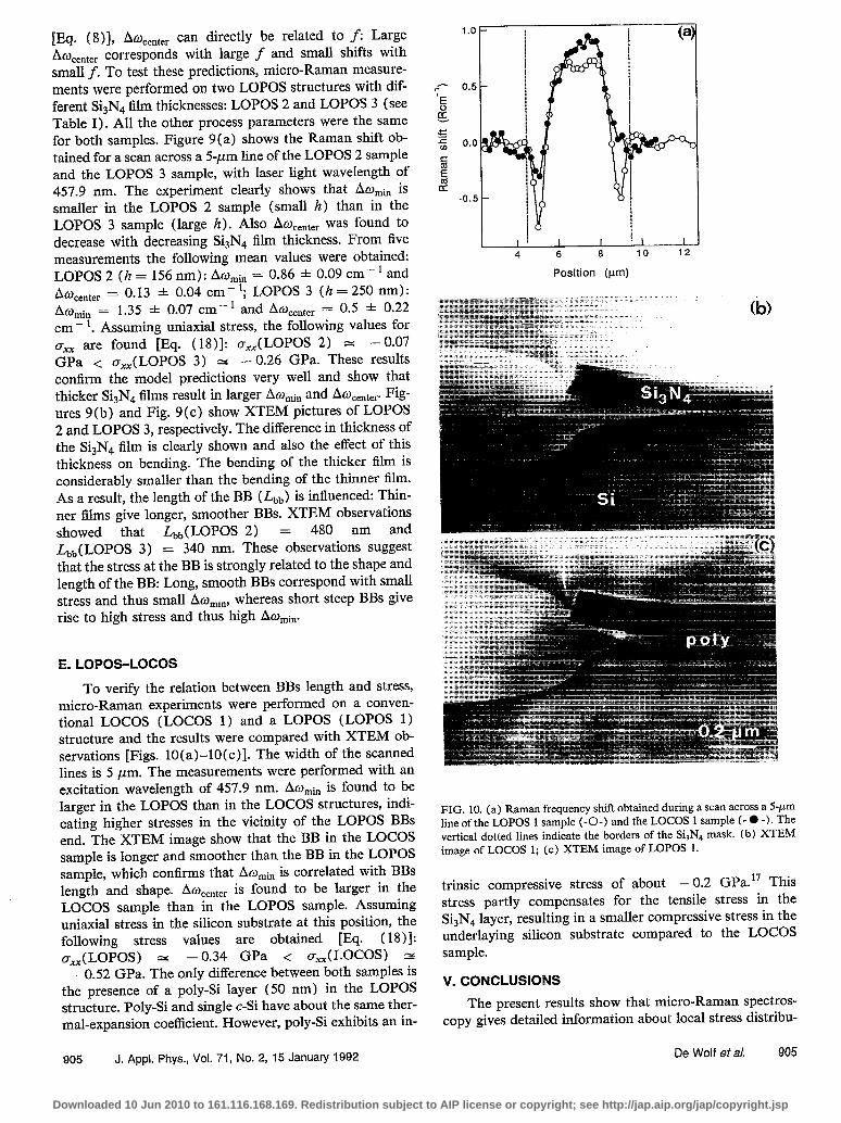
To verify the relation between BBS length and stress, micro-Raman experiments were performed on a conven- tional LOCOS (LOCOS 1) and a LOPOS (LOPOS 1) structure and the results were compared with XTEM ob- servations [Figs. 10(a)-10(c)]. The width of the scanned lines is 5 ,um. The measurements were performed with an excitation wavelength of 457.9 nm. Aw,i” is found to be larger in the LOPOS than in the LOCOS structures, indi- cating higher stresses in the vicinity of the LOPOS BBS end. The XTEM image show that the BB in the LOCOS sample is longer and smoother than the BB in the LOPOS sample, which confirms that Atimin is correlated with BBS length and shape. AwWnter is found to be larger in the LOCOS sample than in the LOPOS sample. Assuming uniaxial stress in the silicon substrate at this position, the following stress values are obtained [Eq. (IS)]: a,( LOPOS) ” - 0.34 GPa < o,,(LOCOS) = - 0.52 GPa. The only difference between both samples is
the presence of a poly-Si layer (50 nm) in the LOPOS structure. Poly-Si and single c-Si have about the same ther- mal-expansion coefficient. However, poly-Si exhibits an in-
905 J. Appl. Phys., Vol. 71, No. 2, 15 January 1992
I I I I , I 4 6 8 10 12
Position (pm)
FIG. 10. (a) Raman frequency shift obtained during a scan across a 5pm line of the LOPOS 1 sample (-0-) and the LOCOS 1 sample (- e -) . The vertical dotted lines indicate the borders of the S&N, mask. (b) XTEM image of LOCOS 1; (c) XTEM image of LOPOS 1.
trinsic compressive stress of about - 0.2 GPa.17 This stress partly compensates for the tensile stress in the Si3N4 layer, resulting in a smaller compressive stress in the underlaying silicon substrate compared to the LOCOS sample.
V. CONCLUSIONS
The present results show that micro-Raman spectros- copy gives detailed information about local stress distribu-
De Wolf et al. 905
Downloaded 10 Jun 2010 to 161.116.168.169. Redistribution subject to AIP license or copyright; see http://jap.aip.org/jap/copyright.jsp

tion in LOCOS and LOPOS isolation structures. It is shown that an increase of the thickness of the S&N4 film and the corresponding reduction of the length of the BB result in an important increase of the local stress at the BBS edge. LOCOS structures with longer and smoother BBS clearly show smaller stress at this position. The stress in the Si substrate under the center of the oxidation mask lines is found to be compressive and to increase with de- creasing linewidth. However, the influence of the large ten- sile stress at the BBS edge on the stress at the center of the lines also increases so that for smaller lines a decrease of the Raman shift and correlated stress is observed. By using different laser wavelengths information of the variation of stress with depth is obtained, indicating a decrease of the stress in depth, with a larger gradient at the BBS edge than at the center of the lines. Despite the fact that a complete fit of the simple planar stress model to the Raman data is not possible, important information can be extracted. Fur- ther progress can be expected by refinement of the model, e.g., by assuming a vertical force distribution instead of one vertical force.
ACKNOWLEDGMENTS
The authors acknowledge the Belgian Fund for Scien- tific Research (NFWO), the Spanish Ministry of Science and Education, and the Swedish Board of Technical De- velopment. The Raman spectroscopy measurements were performed on the equipment of the K. U. Leuven (MTM department) and the XTEM work was performed on the equipment of the University of Antwerp (UCA) .
‘K. Kobayashi, Y. Inoue, T. Nishimura, M. Hirayama, Y. Akasaka, T. Kato, and S. Ibuki, J. Electrochem. Sot. 137, 1987 (1990).
‘Y. Inoue, T. Nishimura, and Y. Akasaka, in Advanced Materiuk for ULS’I, edited by M. Scott, Y. Akasaka, and R. Reif (The Electrochem- ical Society, Pennington, NJ, 1988), p. 233;
‘K. Brunner, G. Abstreiter, B. 0. Kolbesen, and H. W. Meul, in 1989 Proceedings.INFOS, edited by F. Koch and A. Spitzen, 1989, p. 116.
4S. Nadahara, S. Kambayashi, M. Watanabe, and T. Nakakubo, in Ex- tended Abstracts of the 19th Conference on Solid State Devices and Materials, Tokyo, 1987, p. 327.
5S. Kambayashi, T. Hamasaki, T. Nakakubo, W. Watanabe, and H. Tango, in Extended Abstracts of the 19th Conference on SoIid State Devices and Materials, Tokyo, 1986, p. 415.
“R. Loudon, Adv. Phys. 13, 423 ( 1964). ‘S. Ganesan, A. A. Maradudin, and J. Oitmaa, J. Ann. Phys. 56, 556
(1970). *E. Anastassakis, and E Burstein. J. Phys. Chem. Solids 32, 563 (1971). ‘E. Anastassakis, in Proceedings ISPPME ‘85, Varna, Bulgaria: Physical
Problems in Microelectronics, edited by J. Kassabov (World Scientific Publishing Co., Singapore, 1985), p. 128.
‘OS P. Tiioshenko and J. N. Goodier, in Theory of Elasticity, 2nd edi- tion, edited by R. H. Phelps (McGraw-Hill, New York, 1951).
“R. Zeyfang, Solid-State Electron. 14, 1035 (1971). t%. M. Hu, J. Appl. Phys. SO, 4661 (1979). I3 J. Vanhellemont, S. Amelinckx, and C. Claeys, J. Appl. Phys. 61, 2170
(1987). 14E. Anastassakis, in Proceedings Vol. g&11: Analytical Techniques for
Semiconductor Materials and Process Characterization, edited by B. 0. Kolbesen, D. V. MC Caughan, and W. Vandervorst (The Electrochem- ical Society, Pennington, NJ, 1990), p. 298.
Is J. Vanhellemont, C. Claeys, J. Van Landuyt, and S. Amelinckx, in 1985 Proceedings GADEST, edited by H. Richter, p. 255.
161. De Wolf, J. Vanhellemont, A. Romano-Rodriguez, H. Norstrom, and H. E. Maes, in Proceedings of the Third International Symposium on ULSI Science and Technology, The Electrochemical Society, 179th meeting, Washington, DC, May 5-10, 1991.
“S. M. Hu, in Proceedings of the 2nd International Symposium on Process Physics nnd Modeling in Semiconductor Technology (The Electrochem- ical Society, Pennington, NJ, 1991), p. 548.
906 J. Appl. Phys., Vol. 71, No. 2, 15 January 1992 De Wolf eta/. 906
Downloaded 10 Jun 2010 to 161.116.168.169. Redistribution subject to AIP license or copyright; see http://jap.aip.org/jap/copyright.jsp