
Memory Hierarchy Er. Gurpreet Singh Assistant Professor Department of Information Technology,...
56
Memory Hierarchy Er. Gurpreet Singh Er. Gurpreet Singh Assistant Professor Assistant Professor Department of Information Technology, Department of Information Technology, MIMIT Malout MIMIT Malout
-
Upload
gillian-gardner -
Category
Documents
-
view
216 -
download
0
Transcript of Memory Hierarchy Er. Gurpreet Singh Assistant Professor Department of Information Technology,...

Memory Hierarchy
Er. Gurpreet SinghEr. Gurpreet SinghAssistant ProfessorAssistant Professor
Department of Information Technology, Department of Information Technology, MIMIT MaloutMIMIT Malout

Objective Study about the various types of memories

Memory Hierarchy The memory unit is an essential
component in any digital computer since it is needed for storing programs and data
Not all accumulated information is needed by the CPU at the same time
Therefore, it is more economical to use low-cost storage devices to serve as a backup for storing the information that is not currently used by CPU

Memory Hierarchy
Computer Memory Hierarchy is a pyramid structure that is commonly used to illustrate the significant differences among memory types.
The memory unit that directly communicate with CPU is called the main memory
Devices that provide backup storage are called auxiliary memory
The memory hierarchy system consists of all storage devices employed in a computer system from the slow by high-capacity auxiliary memory to a relatively faster main memory, to an even smaller and faster cache memory

MEMORY HIERARCHY
Magnetictapes
Magneticdisks
I/Oprocessor
CPU
Mainmemory
Cachememory
Auxiliary memory
Register
Cache
Main Memory
Magnetic Disk
Magnetic Tape
Memory Hierarchy is to obtain the highest possible access speed while minimizing the total cost of the memory system
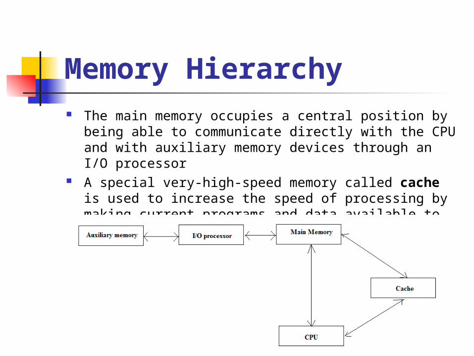
Memory Hierarchy The main memory occupies a central position by being
able to communicate directly with the CPU and with auxiliary memory devices through an I/O processor
A special very-high-speed memory called cache is used to increase the speed of processing by making current programs and data available to the CPU at a rapid rate

Memory Hierarchy CPU logic is usually faster than main memory
access time, with the result that processing speed is limited primarily by the speed of main memory
The cache is used for storing segments of programs currently being executed in the CPU and temporary data frequently needed in the present calculations
The typical access time ratio between cache and main memory is about 1to7
Auxiliary memory access time is usually 1000 times that of main memory


Main Memory Most of the main memory in a general
purpose computer is made up of RAM integrated circuits chips, but a portion of the memory may be constructed with ROM chips
RAM– Random Access memory Integated RAM are available in two possible
operating modes, Static and Dynamic ROM– Read Only memory
Main Memory A RAM chip is better suited for
communication with the CPU if it has one or more control inputs that select the chip when needed
The Block diagram of a RAM chip is shown next slide, the capacity of the memory is 128 words of 8 bits (one byte) per word

RAM
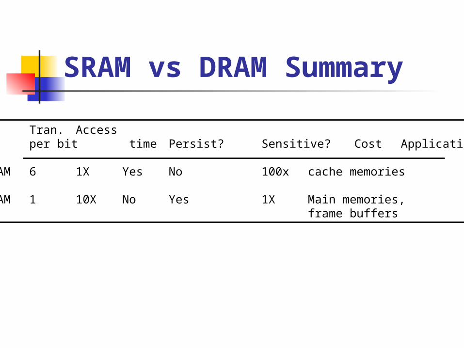
SRAM vs DRAM Summary
Tran. Accessper bit time Persist? Sensitive? Cost Applications
SRAM 6 1X Yes No 100x cache memories
DRAM 1 10X No Yes 1X Main memories,frame buffers

RAM Read/write memory, that initially
doesn’t contain any data The computing system that it is used in
usually stores data at various locations to retrieve it latter from these locations
Its data pins are bidirectional (data can flow into or out of the chip via these pins), as opposite to those of ROM that are output only
It loses its data once the power is removed, so it is a volatile memory
It has a directional select signal R/W’; When R/W’=1, the chip outputs data to the rest of the circuit; when R/W’ = 0 it inputs data from the rest of the circuit

Random-Access Memory Types
Static RAM (SRAM) Each cell stores bit with a six-transistor (Diode) circuit. Retains value indefinitely, as long as it is kept powered. Relatively insensitive to disturbances such as electrical
noise. Faster and more expensive than DRAM.
Dynamic RAM (DRAM) Each cell stores bit with a capacitor and transistor. Value must be refreshed every 10-100 ms. Sensitive to disturbances. Slower and cheaper than SRAM.

Random-Access Memory
Key features RAM is packaged as a chip. Basic storage unit is a cell (one bit per cell). Multiple RAM chips form a memory.
Static RAM (SRAM) Each cell stores bit with a six-transistor circuit. Retains value indefinitely, as long as it is kept powered. Relatively insensitive to disturbances such as electrical noise. Faster and more expensive than DRAM.
Dynamic RAM (DRAM) Each cell stores bit with a capacitor and transistor. Value must be refreshed every 10-100 ms. Sensitive to disturbances. Slower and cheaper than SRAM.

ROM ROM is used for storing programs that are
PERMENTLY resident in the computer and for tables of constants that do not change in value once the production of the computer is completed
The ROM portion of main memory is needed for storing an initial program called bootstrap loader, witch is to start the computer software operating when power is turned off

ROM
Data is programmed into the chip using an external ROM programmer
The programmed chip is used as a component into the circuit
The circuit doesn’t change the content of the ROM Can be used as lookup tables to implement various
functions Used by PCs to store the instructions that form their Basic Input/Output System (BIOS)
When power is removed from a ROM chip, the information is not lost, so it is a nonvolatile type of memory
It has a OE (Output Enable) specific control pin. Both OE and CE must be enabled in order for the ROM to output data; otherwise its data output is tri-stated.

ROM Types Masked ROM – programmed with its data when the
chip is fabricated PROM – programmable ROM, by the user using a
standard PROM programmer, by burning some special type of fuses. Once programmed will not be possible to program it again
EPROM – erasable ROM; the chip can be erased and chip reprogrammed; programming process consists in charging some internal capacitors; the UV light (method of erase) makes those capacitors to leak their charge, thus resetting the chip
EEPROM – Electrically Erasable PROM; it is possible to modify individual locations of the memory, leaving others unchanged; one common use of the EEPROM is in BIOS of personal computers.

ROM

Nonvolatile Memories DRAM and SRAM are volatile memories
Lose information if powered off. Nonvolatile memories retain value even if powered off.
Generic name is read-only memory (ROM). Misleading because some ROMs can be read and modified.
Types of ROMs Programmable ROM (PROM) Eraseable programmable ROM (EPROM) Electrically eraseable PROM (EEPROM) Flash memory
Firmware Program stored in a ROM
Boot time code, BIOS (basic input/ouput system) graphics cards, disk controllers.
Auxiliary Memory
The main memory construction is costly. Therefore, it has to be limited in size. The main memory is used to store only those instructions and data which are to be used immediately. However, a computer has to store a large amount of information. The bulk of information is stored in the auxiliary memory. This is also called backing storageor secondary storage. They include hard disk, floppy disks, CD-ROM, USB flash drives, etc.
When the electricity supply to the computer is off, all data stored in the primary storage is destroyed. On the other hand, this is not true for secondary storage. The data stored in secondary storage can be stored for the desired time.

SOME T I P S FOR
AUXILIARY MEMORY

Disk Geometry Disks consist of platters, each with two surfaces. Each surface consists of concentric rings called
tracks. Each track consists of sectors separated by gaps.
spindle
surfacetracks
track k
sectors
gaps
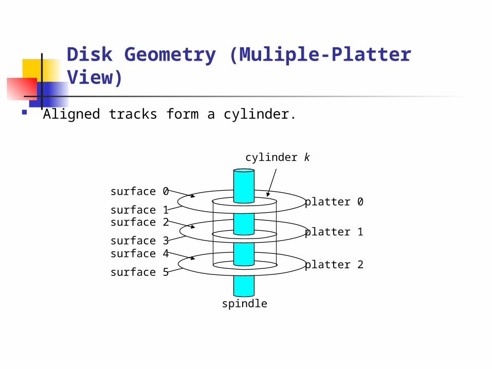
Disk Geometry (Muliple-Platter View)
Aligned tracks form a cylinder.
cylinder k
surface 0
surface 1surface 2
surface 3surface 4
surface 5
spindle
platter 0
platter 1
platter 2

Disk storage Disks are used to store data, applications software
and operating systems software. Whereas the primary form of storage in the early days of computing was magnetic tape, this has been replaced by predominantly disk based medium today. The reasons for this trend has been
decreasing cost per bit reliability reduced access times higher transfer rates (more data per second) reduced size and power requirements increased capacity
One trend during the past few years is a move to optical storage medium. Many software companies offer both operating systems software and application software on optical medium (CDROM or DVDROM)

Disk storage technology
Disk storage systems work on magnetic principles. In magnetism, there are two opposing polarities called poles, the north
and the South pole. Opposite polarity attracts, whilst like polarity repels.
In computers, data is represented in binary format. Binary data has two states, a 1 or a 0. It just so happens that
magnetism also has two states, north and south, so in effect, magnetism is a good way of storing data also
A rotating disk is coated with very fine ferrous oxide particles, each of which act and behave like little magnets
All that is required now is a mechanism of converting the digital data of 0's and 1's into magnetic states of north and south poles.
In a storage disk drive, the mechanism which performs the function of converting the digital 0's and 1's into magnetic states which can magnetize the surface areas of the disk is called the write head. A similar head, called the read head, is used to detect the magnetic states on the surface of the disk and convert them back into digital states

Disk Capacity Capacity: maximum number of bits that can be stored.
Vendors express capacity in units of gigabytes (GB), where 1 GB = 10^9.
Capacity is determined by these technology factors: Recording density (bits/in): number of bits that can be squeezed into
a 1 inch segment of a track. Track density (tracks/in): number of tracks that can be squeezed
into a 1 inch radial segment. Areal density (bits/in2): product of recording and track density.
Modern disks partition tracks into disjoint subsets called recording zones
Each track in a zone has the same number of sectors, determined by the circumference of innermost track.
Each zone has a different number of sectors/track
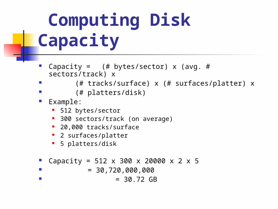
Computing Disk Capacity Capacity = (# bytes/sector) x (avg. # sectors/track) x (# tracks/surface) x (#
surfaces/platter) x (# platters/disk) Example:
512 bytes/sector 300 sectors/track (on average) 20,000 tracks/surface 2 surfaces/platter 5 platters/disk
Capacity = 512 x 300 x 20000 x 2 x 5 = 30,720,000,000 = 30.72 GB

Disk Operation (Single-Platter View)
The disk surface spins at a fixedrotational rate
spindle
By moving radially, the arm can position the read/write head over any track.
The read/write headis attached to the endof the arm and flies over the disk surface ona thin cushion of air.
spin
dle
spindle
spin
dle
spindle

Disk Operation (Multi-Platter View)
armread/write heads move in unisonfrom cylinder to cylinder
spindle

Disk Access Time Average time to access some target sector approximated by :
Taccess = Tavg seek + Tavg rotation + Tavg transfer Seek time (Tavg seek)
Time to position heads over cylinder containing target sector. Typical Tavg seek = 9 ms
Rotational latency (Tavg rotation) Time waiting for first bit of target sector to pass under r/w head. Tavg rotation = 1/2 x 1/RPMs x 60 sec/1 min
Transfer time (Tavg transfer) Time to read the bits in the target sector. Tavg transfer = 1/RPM x 1/(avg # sectors/track) x 60 secs/1 min.

Disk Access Time Example Given:
Rotational rate = 7,200 RPM Average seek time = 9 ms. Avg # sectors/track = 400.
Derived: Tavg rotation = 1/2 x (60 secs/7200 RPM) x 1000 ms/sec = 4
ms. Tavg transfer = 60/7200 RPM x 1/400 secs/track x 1000 ms/sec
= 0.02 ms Taccess = 9 ms + 4 ms + 0.02 ms
Important points: Access time dominated by seek time and rotational latency. First bit in a sector is the most expensive, the rest are free. SRAM access time is about 4 ns/doubleword, DRAM about 60
ns Disk is about 40,000 times slower than SRAM, 2,500 times slower then DRAM.

Optical Disks
The data is accessed from the underside of the CD-ROM. According to the initial specification devised by Philips and Sony, data is stored in a single track which is embedded into a polycarbonate material
The track starts at the inner of the disk, and ends at the outer radius of the disk. The track length is thus one long tightly wound spiral, the equivalent of over 3 miles long
The track is comprised of indentations or bumps which are created on a master disc. This master disc is then used to create the actual CDROM's which are shipped to customers. This technique is similar to the technique which was used to create audio records.
The laser beam is shone onto the surface of the disk. Data is stored as a sequence of surface variations called lands (flat surface) and pits (bumps or holes). The light is scattered by the pits and reflected by the lands. These two variations encode the binary 0's and 1's. The laser beam is moved to follow the spiral track of the data stored on the disk, detected the pits and lands as it follows the spiral track.
A light sensitive diode picks up the reflected laser light from the surface of the disk, and converts the light to digital data.

Optical Disk Technology
The pit and lands vary in length. The speed of rotation of the CD is adjusted so that the speed of the pits and lands passing above the laser is always the same speed (slower when it is in the inner and faster on the outer). This is called Constant Linear Velocity.
The amount of time that occurs between a pit and a land is measured and converted into digital data. Note that the information is stored permanently as pits and lands on the CD-ROM. It cannot be changed once the CD-ROM is mastered, this is why its called CD-ROM.
Single speed CD-ROM has a transfer speed of 150KB/s
DVD (Digital Versatile Disk)
This new standard offers higher data storage and faster data transfers than existing CD-ROM. Differences between DVD and CD-ROM
standard DVD holds 4.7GB per layer, dual layer single sided DVD holds 8.5GB on a single side
error correction is more robust than CD-ROM every DVD is a bonded disc, composed of two 0.6mm substrates
joined together smaller pits are used and tracks are closer together than CD-ROM DVD uses MPEG2 compression for high quality full screen pictures a single layer DVD can hold a two hour 13 minute movie, with full
digital sound in three languages dual layer single sided DVD can hold a movie greater than 4 hours
long DVD-ROM drives have a much faster transfer rate than CD-ROM
drives DVD-ROM drives will read and play existing CD-ROM's and CDA
disks DVD is ideal for companies that wish to deliver enhanced
training that includes high quality video. It has both the storage capacity and transfer speeds to support this type of application. In addition, movie companies are producing full length movie pictures on DVD, as MPEG-2 compression provides full screen high quality definition with multiple language track capability.

Tape Storage Systems Magnetic Reel and Cartridge Tape Digital Audio Tape (DAT) Digital Data Storage (DDS) Digital Linear Tape (DLT)

Cache memory If the active portions of the program
and data are placed in a fast small memory, the average memory access time can be reduced,
Thus reducing the total execution time of the program
Such a fast small memory is referred to as cache memory
The cache is the fastest component in the memory hierarchy and approaches the speed of CPU component

Cache memory
When CPU needs to access memory, the cache is examined
If the word is found in the cache, it is read from the fast memory
If the word addressed by the CPU is not found in the cache, the main memory is accessed to read the word

Cache memory The performance of cache memory
is frequently measured in terms of a quantity called hit ratio
When the CPU refers to memory and finds the word in cache, it is said to produce a hit
Otherwise, it is a miss Hit ratio = hit / (hit+miss)

Cache memory The basic characteristic of cache memory is its
fast access time, Therefore, very little or no time must be
wasted when searching the words in the cache The transformation of data from main memory
to cache memory is referred to as a mapping process, there are three types of mapping:
Associative mapping Direct mapping Set-associative mapping
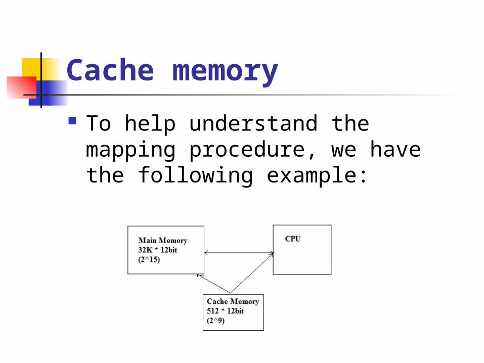
Cache memory
To help understand the mapping procedure, we have the following example:

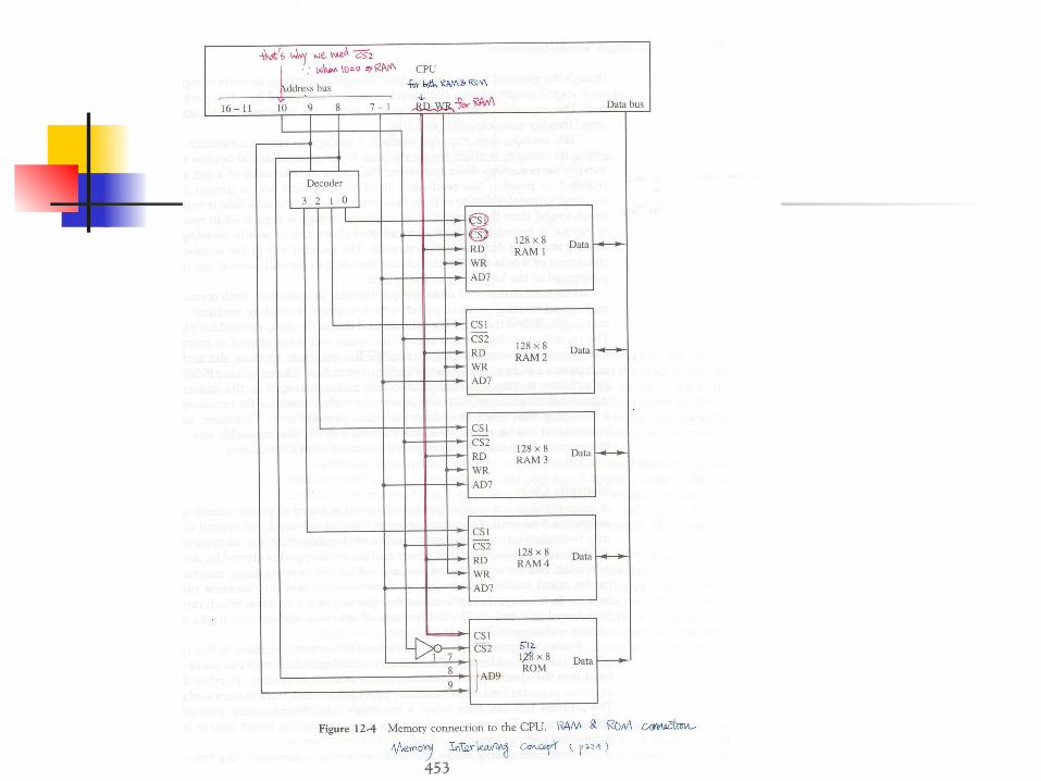
Memory Address Map Memory Address Map is a pictorial
representation of assigned address space for each chip in the system
To demonstrate an example, assume that a computer system needs 512 bytes of RAM and 512 bytes of ROM
The RAM have 128 byte and need seven address lines, where the ROM have 512 bytes and need 9 address lines

Memory Address Map

Memory Address Map The hexadecimal address assigns a range of
hexadecimal equivalent address for each chip
Line 8 and 9 represent four distinct binary combination to specify which RAM we chose
When line 10 is 0, CPU selects a RAM. And when it’s 1, it selects the ROM

Associative mapping The fastest and most flexible cache
organization uses an associative memory The associative memory stores both the
address and data of the memory word This permits any location in cache to store an
word from main memory
The address value of 15 bits is shown as a five-digit octal number and its corresponding 12-bit word is shown as a four-digit octal number

Associative mapping

Associative mapping A CPU address of 15 bits is places in the
argument register and the associative memory searched for a matching address
If the address is found, the corresponding 12-bits data is read and sent to the CPU
If not, the main memory is accessed for the word If the cache is full, an address-data pair must be
displaced to make room for a pair that is needed and not presently in the cache

Direct Mapping Associative memory is expensive
compared to RAM In general case, there are 2^k words in
cache memory and 2^n words in main memory (in our case, k=9, n=15)
The n bit memory address is divided into two fields: k-bits for the index and n-k bits for the tag field

Direct Mapping

Direct Mapping
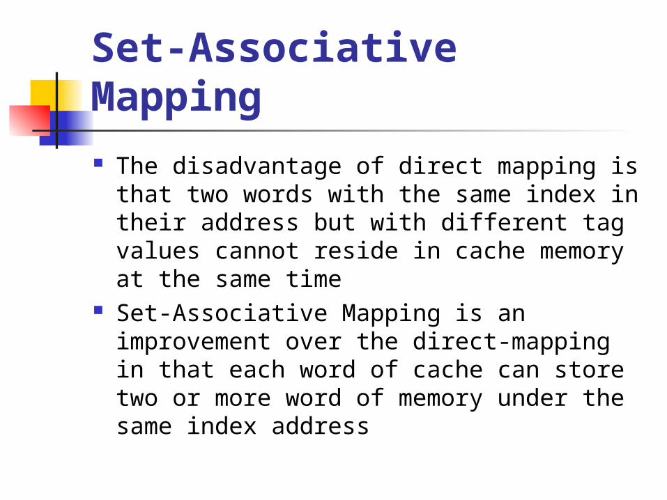
Set-Associative Mapping The disadvantage of direct mapping is
that two words with the same index in their address but with different tag values cannot reside in cache memory at the same time
Set-Associative Mapping is an improvement over the direct-mapping in that each word of cache can store two or more word of memory under the same index address

Set-Associative Mapping

Set-Associative Mapping
In the slide, each index address refers to two data words and their associated tags
Each tag requires six bits and each data word has 12 bits, so the word length is 2*(6+12) = 36 bits


THANKSTHANKS