
Mechanical, Optical and Electrical Properties of Nano-polished CVD Diamond Films
32
Department of Electronic Devices J.A. Weima Mechanical, Optical and Electrical Properties of Nano-polished ... Mechanical, Optical and Electrical Properties of Nano-polished CVD Diamond Films J. A. Weima 1) , J. von Borany 2) , and W. R. Fahrner 1) 1) Department of Electronic Devices, University of Hagen, Haldener Str. 182, D-58084 Hagen, Germany 2) Institute of Ion Beam Physics and Materials Research P.O. Box 510119, D-01314 Dresden, Germany
Transcript of Mechanical, Optical and Electrical Properties of Nano-polished CVD Diamond Films
Department of Electronic Devices
J.A. Weima Mechanical, Optical and Electrical Properties of Nano-polished ...
Mechanical, Optical and Electrical
Properties of Nano-polished CVD
Diamond Films
J. A. Weima1), J. von Borany2), and W. R. Fahrner1)
1) Department of Electronic Devices, University of Hagen,
Haldener Str. 182, D-58084 Hagen, Germany2) Institute of Ion Beam Physics and Materials Research
P.O. Box 510119, D-01314 Dresden, Germany

Department of Electronic Devices
J.A. Weima Mechanical, Optical and Electrical Properties of Nano-polished ...
Contents
1. Introduction
2. Description of the polishing machine
3. Experimental results:
(i) SEM and AFM images of as-grown,
polished and beveled surfaces
(ii) Carbon phases and optical centers
determined by Raman spectroscopy
(iii) CL Spectra
(iv) ERDA depth distribution of carbon
(v) RBS determination of surface
contaminants
(vi) I-V and EL spectra of polished CVD
diamond films
4. Summary and Conclusion

Department of Electronic Devices
J.A. Weima Mechanical, Optical and Electrical Properties of Nano-polished ...
Introduction:Polishing procedure:
i) CVD diamond films polished on transition metals (steel)
ii) Ambient Atmosphere; mixture of hydrogen-argon
(4% - 96%), ambient temperature (700-950 °C), pressure
exerted on the diamond film (1-2 kPa), velocity of the
polishing plate (1-3 cm/s), frequency and amplitude of
the transversal vibrations
Applications:
Thermal management, optical windows, wear tools, micro-
surgical equipment, electronic and opto-electronic devices
Motivation:
i) Investigating various non-diamond carbon phases, carbon
dissolution in steel: Model of thermochemical polishing
ii) Investigating optical centers and contaminants and their
location on the polished diamond surfaces: Enhancement
of defect free device fabrication
iii) Comparative study of I-V characteristics of polished and
unpolished CVD diamond films: Effect of polishing on
performance of diamond-base devices

Department of Electronic Devices
J.A. Weima Mechanical, Optical and Electrical Properties of Nano-polished ...
The Thermochemical Polishing Machine
Diamond Sample
ScanningThermometer
Thermo-Couple
Gas Inlet
Chamber
Hot wire-Tungsten
WaterInlet
DriveBoard
FrequencyGenerator
Cover forChamberMain
PowerSupply Heat
Reflectors
Ceramic
Motor
PowerSupply
WaterOutlet
AdditionalDrive Board
PowerSupply
DriveBoard
Weight
Motor
PolishingPlateFrequency
Generator

Department of Electronic Devices
J.A. Weima Me
SEM micrograph of growth side of an as-grown CVDdiamond film x 200
chanical, Optical and Electrical Properties of Nano-polished ...
Grain boundaries

Department of Electronic Devices
J.A. Weima Mechanical, Optical and Electrical Properties of Nano-polished ...
SEM micrograph of the growth side of a polished CVDdiamond film x 5000
Department of Electronic Devices
J.A. Weima Mechanical, Optical and Electrical Properties of Nano-polished ...
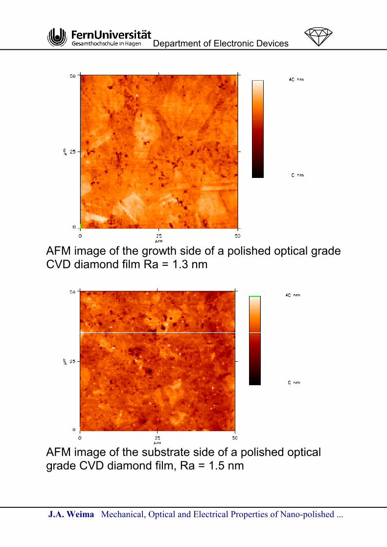
AFM image of the growth side of a polished optical gradeCVD diamond film Ra = 1.3 nm
AFM image of the substrate side of a polished opticalgrade CVD diamond film, Ra = 1.5 nm

Department of Electronic Devices
J.A. Weima Mechanical, Optical and Electrical Properties of Nano-polished ...
An SEM image of a diamond CVD diamond filmbeveled successively on both sides at 15°. Thecutting edge with a radius of curvature of about50 nm is formed at the intersection of the twobeveled facets.
Department of Electronic Devices
J.A. Weima Mechanical, Optical and Electrical Properties of Nano-polished ...
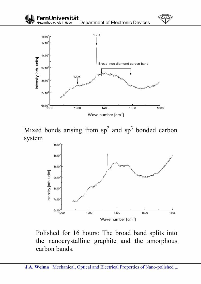
Mixed bonds arising from sp2 and sp3 bonded carbonsystem
Polished for 16 hours: The broad band splits intothe nanocrystalline graphite and the amorphouscarbon bands.
1000 1200 1400 1600 18006x103
7x10³
8x10³
9x10³
1x10⁴
1x10⁴
1x10⁴
Inte
nsity
[arb
. uni
ts]
Wave number [cm-1]
1000 1200 1400 1600 18006x103
7x10³
8x10³
9x10³
1x10⁴
1x10⁴
1x10⁴
1206
Broad non-diamond carbon band
1331In
tens
ity [a
rb. u
nits
]
Wave number [cm-1]

Department of Electronic Devices
J.A. Weima Mechanical, Optical and Electrical Properties of Nano-polished ...
Further polishing: The microcrystalline graphiteband appear in addition to the previous bands.
Further polishing: The entire diamond surface isnow covered only by the two graphite bands.
1000 1200 1400 1600 18002,0x103
4,0x10³
6,0x10³
8,0x10³
1,0x10⁴
1,2x10⁴
1,4x10⁴
1,6x10⁴
1,8x10⁴
1331 1580
14781353
Inte
nsity
[arb
. uni
ts]
Wave number [cm-1]
1000 1200 1400 1600 18000
1x10³
2x10³
3x10³
4x10³
5x10³
6x10³
1580
1353
Nanocrystalline
graphite
M icrocrystalline
graphite
Inte
nsity
[arb
. uni
ts]
Wave number [cm-1]

Department of Electronic Devices
J.A. Weima Mechanical, Optical and Electrical Properties of Nano-polished ...
Polishing at low temperature (800 °C): The non-diamond carbon dissolves into the metal.
Final polishing at much lower temperature (750°C): The entire diamond surface is free of non-diamond carbon phases
1000 1200 1400 1600 1800-1,0x10³
0,0
2,0x10³
4,0x10³
6,0x10³
8,0x10³
1,0x10⁴
1,2x10⁴
1,3x10⁴
1578
1331In
tens
ity [a
rb u
nits
]
Wave number [cm-1]
1000 1100 1200 1300 1400 1500 1600 1700 1800
0,0
2,0x10³
4,0x10³
6,0x10³
8,0x10³
1,0x10⁴
1,2x10⁴
1,4x10⁴ 1331 cm-1
Inte
nsity
[arb
. uni
ts]
Wave number [cm-1]

Department of Electronic Devices
J.A. Weima Mechanical, Optical and Electrical Properties of Nano-polished ...
Raman spectra of a thermochemically polished optical grade
CVD diamond film. Low frequency Raman lines (100-700
cm-1) are seen for the first time. The lines are tentatively
attributed to clusters of carbon particles left on the polished
surfaces.
200 400 600 800 1000 1200 1400 1600-1,0x10³
0,0
5,0x10³
1,0x10⁴
1,5x10⁴
2,0x10⁴
1580
1352
657585
485
392
280215
Inte
nsity
[cou
nts]
Wave number [cm-1]

Department of Electronic Devices
J.A. Weima Mechanical, Optical and Electrical Properties of Nano-polished ...
Raman spectra of an as-grown CVD diamond film taken atthree different spots. The spectra show the diamond Ramanline, the nitrogen-vacancy defect centers and the silicon-vacancy defect center.
0 1000 2000 3000 4000 5000 6000
1.6x10⁴
1.2x10⁴
8.0x10³
4.0x10³
0.0
diamond-Raman line1332
Si-V band
N-V- band
N-V0 bond
5894
37742068
Inte
nsity
[cou
nts]
Wave number [cm-1]

Department of Electronic Devices
J.A. Weima Mechanical, Optical and Electrical Properties of Nano-polished ...
Raman spectra of a polished CVD diamond film taken at threedifferent spots. In addition to the bands seen in the as-grownfilm, bands of nanocrystalline graphite, microcrystallinegraphite, nitrogen molecules, and hydrogen molecules are alsoobserved.
0 1000 2000 3000 4000 5000 6000
0
1x10³
2x10³
3x10³
4x10³
5x10³
N2
Diamond
lineH2
N-V- Si-V N-Vo
Graphite bands
C-Hn vibrations
Inte
nsity
[cou
nts]
Wave number [cm-1]
Department of Electronic Devices
J.A. Weima Mechanical, Optical and Electrical Properties of Nano-polished ...
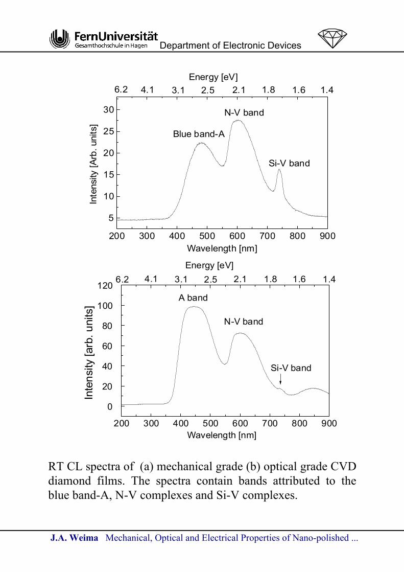
RT CL spectra of (a) mechanical grade (b) optical grade CVDdiamond films. The spectra contain bands attributed to theblue band-A, N-V complexes and Si-V complexes.
200 300 400 500 600 700 800 900
0
20
40
60
80
100
120
Energy [eV]1.41.61.82.12.53.14.16.2
Si-V band
N-V band
A band
Inte
nsity
[arb
. uni
ts]
Wavelength [nm]
200 300 400 500 600 700 800 900
5
10
15
20
25
30
Energy [eV]1.41.61.82.12.53.14.16.2
Si-V band
N-V band
Blue band-A
Inte
nsity
[Arb
. uni
ts]
Wavelength [nm]

Department of Electronic Devices
J.A. Weima Mechanical, Optical and Electrical Properties of Nano-polished ...
(a) (b)
(c) (d)
(e)
SEM-SE and the monochromatic 438 nm, 605 nm, 845 nm CLimages of an as-grown CVD diamond film showing the regionsof luminescence.
200 300 400 500 600 700 800 9000
50
100
150
200
2nd Order blue band-A
N-V band
blue band-A
Energy [eV]1.381.552.07 1.772.483.104.146.20
Inte
nsity
[%]
Wavelength [nm]

Department of Electronic Devices
J.A. Weima Mechanical, Optical and Electrical Properties of Nano-polished ...
0 50 100 150 200 250 3000,0
0,1
0,2
0,3
0,4
0,5
0,6
0,7
0,8ERDA: 35Cl7+, 35 MeV
Polishing Plates(1.220 /115CrV3)
Process Time virgin 0,5 h 1,0 h 4,0 h 8,0 h
carb
on c
once
ntra
tion
(x10
23cm
-3)
depth (nm)
0
10
20
30
40
50
60
70
80
90
car
bon
cont
ent (
at.-
%)
ERDA carbon depth profiles in steel measured for polishingtimes between 0-8 hours. The profiles clearly confirm thedissolution of carbon in steel during the polishing.

Department of Electronic Devices
J.A. Weima Mechanical, Optical and Electrical Properties of Nano-polished ...
0 50 100 150 200 250 3000,0
0,1
0,2
0,3
0,4
0,5
0,6
0,7
0,8ERDA: 35Cl7+, 35 MeV
Polishing Plates(1.220 /115CrV3)
virgin S1: 8h S2: 8h S3: 8h
carb
on c
once
ntra
tion
(x10
23cm
-3)
depth (nm)
0
10
20
30
40
50
60
70
80
90
car
bon
cont
ent (
at.-
%)
ERDA carbon depth profiles in three steel plates on whichCVD diamond films were successively polished for 8 hours.An non-homogeneous distribution of carbon is observedespecially in the first 50 nm from the surface.

Department of Electronic Devices
J.A. Weima Mechanical, Optical and Electrical Properties of N
Determination of D(x,t) by fitting experimental restheoretical values.
+−−∞= ietNxNtxN **),0()140/exp(1),( π
Calculated value: D(x,t) = 1.16 x 10⁻¹⁴ cm2/s.
0 50 100 150 200 250
3.5
3.0
2.5
2.0
1.5
1.0
0.5
0.0
D = 1.16 x 10⁻¹⁴ cm2s-1 0 hour calculated 0 hour experiment 4 hours calculated 4 hours experiment 8 hours experiment 8 hours calculated
Con
cent
ratio
n x
1022
[cm
-3]
Depth [nm]
ano-polished ...
ults to
Dtxrfc
2
300 350

Department of Electronic Devices
J.A. Weima Mechanical, Optical and Electrical Properties of N
ano-polished ...
Department of Electronic Devices
J.A. Weima Mechanical, Optical and Electrical Properties of Nano-polished ...

Department of Electronic Devices
J.A. Weima Mechanical, Optical and Electrical Properties of Nano-polished ...
Experimental and simulated RBS spectra of the surface of aCVD diamond film thermo-chemically polished on steel at950 °C for 8 hours. Iron found at depths within 120 nm fromthe surface is the only detectable contaminant.
Fe

Department of Electronic Devices
J.A. Weima Mechanical, Optical and Electrical Properties of Nano-polished ...
200 300 400 500 600 700 8000
50
100
150
200
2501.73 / 20
FZ R
osse
ndor
f: G
rötz
sche
l / v
on B
oran
y, 7
.03.
00
Simulation:Lay 1: d = 40 nm C:Fe=99.2:0.8Lay 2: Bulk C=100
1.7 MeV, 4He+
10 µC, 0°, rs
Samples: FU Hagen, ElektrotechnikCVD-Diamond, Nanopolished: 25 h, 950°CSubstrate side
D2: as polished D3: polished + etched D2 - Simulation
RB
S y
ield
channel number
0,4 0,6 0,8 1,0 1,2 1,4
energy (MeV)
Experimental RBS spectra of two CVD diamond filmspolished at 950 °C for 25 hours each. The as-polished filmcontain iron at depths within 40 nm from the surface is theonly contaminant. The film etched in chromic acid is virtuallyfree from iron contaminants.
Fe

Department of Electronic Devices
J.A. Weima Mechanical, Optical and Electrical Properties of Nano-polished ...
RT and 300 °C I-V characteristics of p-i-n, p-i-p and n-i-ndiodes with L=5 µm fabricated on a thermochemicallypolished CVD diamond film. The RT leakage current of the p-i-n diode is smallest while that of the p-i-p is about an orderhigher. Moreover, the forward current of the p-i-n diode isabout 2 orders of magnitude higher than those of the p-i-p andn-i-n diodes.
0,1 1 10 100 10001x10-13
1x10-12
1x10-11
1x10⁻¹⁰
1x10⁻⁹
1x10⁻⁸
1x10⁻⁷
1x10⁻⁶
1x10⁻⁵
1x10⁻⁴
1x10⁻³
1x10⁻²
p-i-n RT p-i-p RT n-i-n RT p-i-n 300 °C p-i-p 300 °C n-i-n 300 °C
Cur
rent
[A]
Voltage [V]

Department of Electronic Devices
J.A. Weima Mechanical, Optical and Electrical Properties of Nano-polished ...
The I-V characteristics at 300 °C of p-i-n diodes with thei-region varying from 3-10 µm showing both the forward andreverse bias regimes. A comparison of the current values atforward and reverse biases of 60 V shows that the forwardbias current is 1.8, 2.4, 2.8 and 3.6 orders of magnitude higherthan the reverse bias current for L = 3, 5, 8 and 10 µm,respectively.
-60 -50 -40 -30 -20 -10 0 10 20 30 40 50 60
1x10-12
1x10-11
1x10⁻¹⁰
1x10⁻⁹
1x10⁻⁸
1x10⁻⁷
1x10⁻⁶
1x10⁻⁵
1x10⁻⁴
1x10⁻³
1x10⁻²
CVD diamond-base p-i-n diodes
p-i-n (3µm) 300 °C p-i-n (5µm) 300 °C p-i-n (8µm) 300 °C p-i-n (10µm) 300 °C
Cur
rent
[A]
Voltage [V]

Department of Electronic Devices
J.A. Weima Mechanical, Optical and Electrical Properties of Nano-polished ...
Current-voltage characteristics of a p-i-n diode with L=8 µm.The asymmetric trend of the curves is due to the difference inthe forward and reverse bias currents of the p-i-n diode.
-120 -100 -80 -60 -40 -20 0 20 40 60 80 100 1201x10-14
1x10-12
1x10⁻¹⁰
1x10⁻⁸
1x10⁻⁶
1x10⁻⁴
1x10⁻²
p-i-n diode: L = 8 µmn common
T=RT T=50 °C T=100 °C T=150 °C T=200 °C T=250 °C T=300 °C
Curre
nt [A
]
Voltage [V]

Department of Electronic Devices
J.A. Weima Mechanical, Optical and Electrical Properties of Nano-polished ...
Current-voltage characteristics of a p-i-p diode with L=10 µm.The symmetric trend of the curves is due to successiveinjection of carriers across the p-i junctions of the identicallydoped p-regions of the p-i-p diode. The I-V characteristicsholds for n-i-n diodes as well.
-120 -100 -80 -60 -40 -20 0 20 40 60 80 100 12010-12
10-11
10-10
10-9
10-8
10-7
10-6
10-5
10-4
p-i-p diode: L = 10µm
T=RT T=50 °C T=100 °C T=150 °C T=200 °C T=250 °C T=300 °C
Cur
rent
[A]
Voltage [V]

Department of Electronic Devices
J.A. Weima Mechanical, Optical and Electrical Properties of Nano-polished ...
EL spectra of CVD diamond-base p-i-p, p-i-n and n-i-n diodesfabricated on a thermochemically polished CVD diamondfilm. A blue band-A at 2.85 eV is attributed to dislocationsand a red band at 1.84 eV is attributed to the recombination ofdonor-acceptor pair.
350 400 450 500 550 600 650 700 7502
4
6
8
10
12
14
16
18
20
22
Red band
Blue band-A
Electron Energy [eV]1.651.771.912.072.262.482.763.103.55
p-i-p; 0.2 mA - 305 V n-i-n; 0.2 mA - 280 V p-i-n; 0.2 mA - 260 V
EL in
tens
ity [a
rb. u
nits
]
Wavelength [nm]

Department of Electronic Devices
J.A. Weima Mechanical, Optical and Electrical Properties of Nano-polished ...
EL spectra of a p-i-n diode with L = 8 µm taken at increasingcurrent and voltages. The maximum of the blue band-A isconstant at about 2.85 eV and its intensity increases linearlywhereas the intensity of the red band is saturated.
350 400 450 500 550 600 650 700 750
10
20
30
40
50
60
Electron Energy [eV]
Red band
Blue band-A
1.651.771.912.072.262.482.763.103.55
0.2 mA - 280 V 0.4 mA - 490 V 0.6 mA - 540 V
EL in
tens
ity [a
rb. u
nits
]
Wavelength [nm]

Department of Electronic Devices
J.A. Weima Mechanical, Optical and Electrical Properties of Nano-polished ...
RT I-V characteristics of p-i-p diodes fabricated on (a): athermochemically polished CVD diamond film and (b): an as-grown CVD diamond film. The I-V curves of the polish filmare more diode-like than those of the unpolished film.
0,1 1 10 100 10001x10-13
1x10-12
1x10-11
1x10⁻¹⁰
1x10⁻⁹
1x10⁻⁸
1x10⁻⁷
1x10⁻⁶
1x10⁻⁵
1x10⁻⁴
1x10⁻³
FP-SCLC regime
FP-TE regime
Trap filling regime
p-i-p diodes on a polishedCVD diamond film RT: ~23 °C
L=5 µm L=7.5 µm L= 10 µm
Cur
rent
[A]
Voltage [V]
0,1 1 10 100 10001x10-13
1x10-12
1x10-11
1x10⁻¹⁰
1x10⁻⁹
1x10⁻⁸
1x10⁻⁷
1x10⁻⁶
1x10⁻⁵
1x10⁻⁴
1x10⁻³
p-i-p diodes on an unpolished CVD diamond filmTemp: ~ 23 °C
L=5 µm L=7.5 µm L=10 µm
Cur
rent
[A]
Voltage [V]
Department of Electronic Devices
J.A. Weima Mechanical, Optical and Electrical Properties of Nano-polished ...
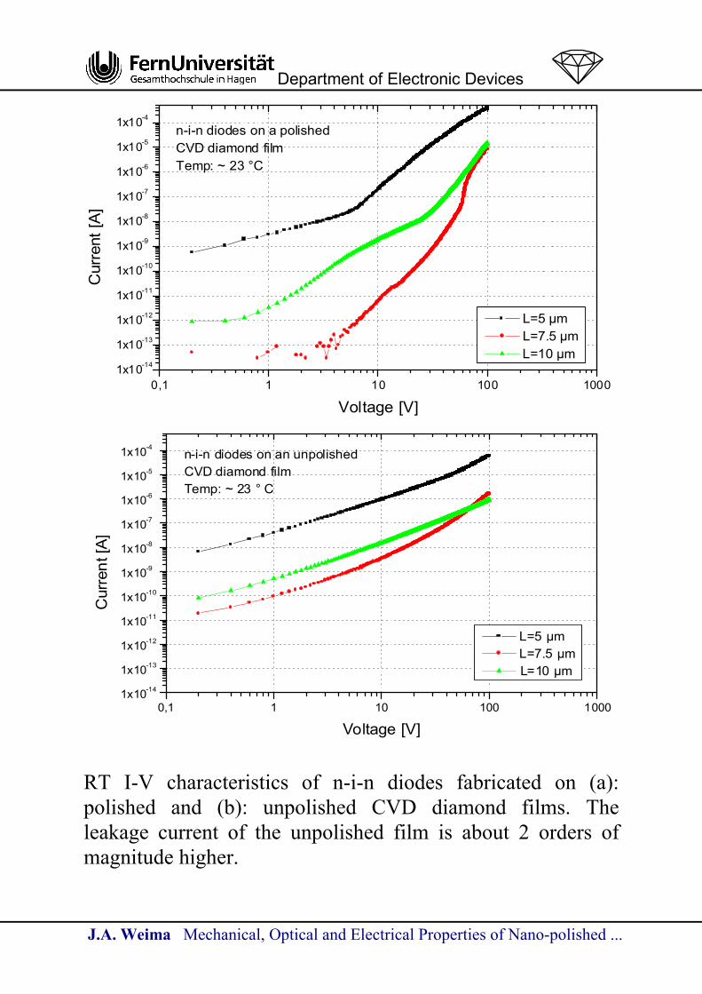
RT I-V characteristics of n-i-n diodes fabricated on (a):polished and (b): unpolished CVD diamond films. Theleakage current of the unpolished film is about 2 orders ofmagnitude higher.
0,1 1 10 100 10001x10-14
1x10-13
1x10-12
1x10-11
1x10⁻¹⁰
1x10⁻⁹
1x10⁻⁸
1x10⁻⁷
1x10⁻⁶
1x10⁻⁵
1x10⁻⁴
n-i-n diodes on a polishedCVD diamond filmTemp: ~ 23 °C
L=5 µm L=7.5 µm L=10 µm
Cur
rent
[A]
Voltage [V]
0,1 1 10 100 10001x10-14
1x10-13
1x10-12
1x10-11
1x10⁻¹⁰
1x10⁻⁹
1x10⁻⁸
1x10⁻⁷
1x10⁻⁶
1x10⁻⁵
1x10⁻⁴n-i-n diodes on an unpolished CVD diamond filmTemp: ~ 23 ° C
L=5 µm L=7.5 µm L=10 µm
Cur
rent
[A]
Voltage [V]

Department of Electronic Devices
J.A. Weima Mechanical, Optical and Electrical Properties of Nano-polished ...
Summary and Conclusion
(1) Carbon phases include nano- and microcrystalline
graphite, amorphous carbon; Complexes include
C-Hn, H2 and N2 complexes
(2) Best AFM Surface roughness result 1.3 nm
(3) Dissolution of carbon in steel confirmed by depth
profiles: Diffusion constant of 1.16 x 10⁻¹⁴ cm2s-1
(4) Optical centers include Si-V, N-V0, N-V-1 and blue
band-A found in the CL and EL spectra as well
(5) Iron is the only detectable surface contaminant
(6) (i) Photolithography is effectively achieved only
on nano-polished surfaces
(ii) The leakage current of diodes on unpolished
diamond is about 2 orders of magnitude
higher
(iii) p-i-n diodes deliver highest current at higher
voltages in comparison to p-i-p and n-i-n.
(iv) The ratio of the forward to reverse bias
current increases with increasing L for the
measured diodes.