Low Power IP Design Methodology for Rapid Development of DSP Intensive SOC Platforms
61
Low Power IP Design Methodology for Rapid Development of DSP Intensive SOC Platforms T. Arslan A.T. Erdogan S. Masupe C. Chun-Fu D. Thompson
-
Upload
kareem-wright -
Category
Documents
-
view
25 -
download
2
description
Low Power IP Design Methodology for Rapid Development of DSP Intensive SOC Platforms. T. Arslan A.T. Erdogan S. Masupe C. Chun-Fu D. Thompson. Contents. Introduction to power consumption Introduction to Main Concepts Low Power Design Methodology IP implementations Results and conclusions. - PowerPoint PPT Presentation
Transcript of Low Power IP Design Methodology for Rapid Development of DSP Intensive SOC Platforms

Low Power IP Design Methodology for Rapid Development of DSP Intensive SOC Platforms
T. ArslanA.T. ErdoganS. MasupeC. Chun-Fu
D. Thompson

Contents
• Introduction to power consumption
• Introduction to Main Concepts
• Low Power Design Methodology
• IP implementations
• Results and conclusions

Power Consumption in CMOS-Based DSP Systems
Vdd
VoutinV
C L
I sc Idy
Idd = I sc Idy+
I sc
V
Idy
V
t
out
in
P k.C.V . f I .V I Vave dd sc dd l dd 2
Power ReductionMethods
Reduce
C*= k.C
ReduceVdd

• Supply Voltage Reduction
• Clock Gating
Disadvantage:
• Added design effort
Common Approaches to Low Power Design

Systematic Low Power Design Approach
Exploit Algorithmic Correlations and Redundancies within an algorithm, then Map to hardware.

Verilog/VHDL
DSP AlgorithmLibrary
PerformanceCriteria
Block,Segmentation, etc.
Multiplier SC,Bus SC CAD
SynthesisComponent
Library
Ordering algorithm
Data representation
Netlist
Systematic Design Implementation Framework

Rapid Design and IP-Based Integration Platforms
. . .
P
IPy
IPx
. . .

Developed IPs

Parameterisation Options

Synthesis(Buildgate)
System Design(Verilog)
Verification(Behavioural Simulation)
Technology-SpecificNetlist
Verification(Gate-Level Simulation)
Verification(Post-Layout Simulation)
Floorplanning,Placement & Routing(Silicon Ensemble)
I/O PadsPlacement
Tape-out Verification(Dracula DRC/ERC/LVS)
SystemSpecifications
Layout
Design Flow for Filter IPs

FIR Filter Implementation

Typical Single Multiplier DSP Processor Architecture
Multiplier
Adder
Output register
Control
ADCinput
x(n)
DACoutput
y(n)
Data bus
Coefficient bus
Datamemory
Coefficientmemory
Multiplier-accumulator(MAC)

Transpose Direct Form (TDF) FIR Structure
x(n)
z-1z-1
h(0) h(1) h(2)
y(n)
h(N-1)
z-1. . .
. . .
. . .
stage0 stage1stage1. . . stageN-1
PCV1(n)PCV1(n) PCV2(n) PCVN-1(n)PCV0(n)

Multiplier
Adder
Control
ADCinput
x(n)
DACoutput
y(n)
Data bus I
Coefficient bus
PCVMCoefficient
memory
Data bus II
Modified DSP Processor Architecture for TDF FIR Filter Implementation

An Example SFG for IP2

Coefficient Memory Configuration with Coefficient Ordering
Order coefficients such that adjacent coefficients are highly correlated.
Filter Design(Matlab)
FilterSpecifications
Coefficient Set
Coefficient Ordering(C Routine)
OrderedCoefficient Set
Memory Configuration(C Routine)
Coefficient Words

Coefficient Word:
SF : Shift Flag
SF = 1 shift
SF = 0 no shift
PCVMA : Pre-Calculated Value Memory Address
h(k) PCVMA SF

Coefficient Word Decomposition (Verilog Code)

An Example SFG for IP3

Memory Operations (Verilog Code)

Software Implementation Example for IP3

Power Evaluation

Filter Specifications
Lowpass filter specifications
Filter #Passband
(kHz)Stopband
(kHz)
Passbandripple(dB)
Stopbandattenuation
(dB)
Windowfunction
Filterlength
1 0 - 1.5 2 - 4 0.1 50 Hamming 532 0 - 1.2 1.7 - 5 0.01 40 Kaiser 713 0 - 3.375 5.625 - 10 0.002 90 - 424 0 - 1 1.5 - 5 0.0135 56 - 615 0 - 1.5 2 - 4 0.1 50 Blackman 89
Bandpass filter specifications
Filter #Stopband
(kHz)Passband
(kHz)Stopband
(kHz)
Passbandripple(dB)
Stopbandattenuation
(dB)
Windowfunction
Filterlength
1 0 - 0.1 0.15 - 0.25 0.3 - 0.5 0.1 60 Kaiser 732 0 - 0.45 0.9 - 1.1 1.55 - 7.5 0.8 30 - 343 0 -5 8 - 12 15 - 44.14 0.00868 60 Kaiser 544 0 - 1 2 - 3.5 4.25 - 5 0.13 56.4 - 325 0 - 0.1 1.375-3.625 4 - 5 0.1 68.4 - 80

0
500
1000
1500
2000
2500
3000
3500
4000
4500
5000
swit
ched
cap
acit
ance
(p
F)
IP1 IP2 IP3
PCVM bus
coefficient bus
data bus
multiplier
25%
54%
Power Reductions Achieved (wordlength = 16 bit)

An example of a 6-tap FIR filter with block size of 3

Power Reductions for IP4 (wordlength = 16 bit)
0
100
200
300
400
500
600
700
800
900
swit
ched
cap
acit
ance
(p
F)
1 2 4 8 16
Block Size
coefficient bus
data bus
multiplier
40% 42%
50%53%

Reductions in Number of Memory Accesses (%)
0
10
20
30
40
50
60
70
80
90
100
Red
uct
ion
(%
)
2 4 8 16
Block Size
Data memory
Coefficient memory

Coefficient Set
Coefficient Set1 Coefficient Set2
Data Set
Shifter
Multiplier
Adder
Output
Coefficient Segmentation Algorithm

Example Segmentations

Example Segmentations

Coefficient Segmentation Algorithm for Two’s Complement Coding
Begin
H = (h0, h1, … , hL-1)
i = 0, k = 0
2i >= hk i = i + 1
sk = 2i-1
sk = - 2i
k > L -1i = 0
k = k + 1
End
No
No
No
Yes
Yes
Yes
3 hk <= 0
mk = 0
sk = hkNo
Yes
2 2i != hk
1
mk = hk-sk
mk = hk-sk

Coefficient Segmentation Algorithm for Sign-Magnitude Coding
Begin
H = (h0, h1, … , hL-1)
i = 0, k = 0
2i >= hk i = i + 1
mk = hk - 2i-1
sk = 2i-1hk
- 2i < hk - 2i-1
mk = hk - 2i
sk = 2i
hk < 0
mk = - mk
sk = - sk
k > L -1i = 0
k = k + 1
End
No
No
No
No
Yes
Yes
Yes
Yes
1
2
3

Total switching activity of H and M coefficient sets with Two’s Complement Coding

Total switching activity of H and M coefficient sets with Sign-Magnitude Coding

MSB(coefficient)
(two’s complement)
(sign magnitude)
Multiplier(two’s)
Add/Sub
Acc
Control
CoefficientMemory
DataMemory
Output
Simplified Filter Architecture for Mixed-Mode Multiplication

( sign magnitude)
( sign magnitude)
Multiplier(sign)
Add
Acc
Control
CoefficientMemory
DataMemory
Sign two’s
Output
Simplified Filter Architecture for Sign-Magnitude Multiplication

0
5
10
15
20
25
30
35
40
45
#Tra
nsi
tio
ns/
sam
ple
b0 b2 b4 b6 b8 b10
b12
b14
Bit Position
conventional
segmentation
Example Switching Activity Distribution with Two’s Complement Coding (N=89, W=16)

0
5
10
15
20
25
30
35
40
45
50
#Tra
nsi
tio
ns/
sam
ple
b0 b2 b4 b6 b8 b10
b12
b14
Bit Position
conventional
segmentation
Example Switching Activity Distribution with Sign-Magnitude Coding (N=89, W=16)
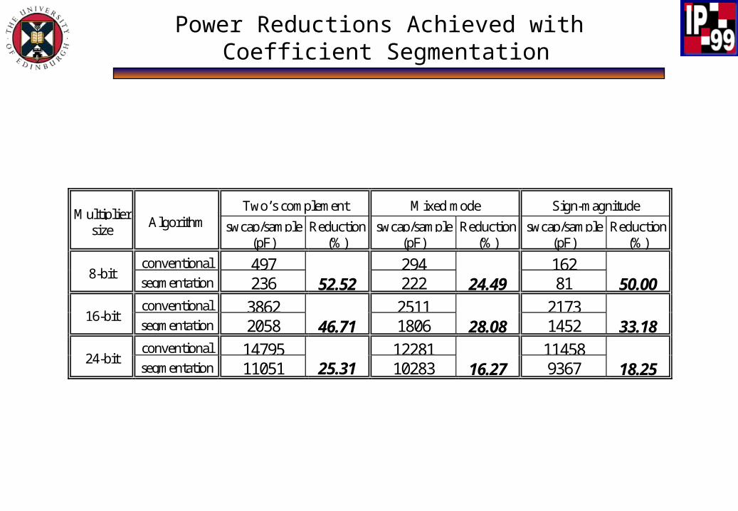
Two’s complement Mixed mode Sign-magnitudeMultiplier
sizeAlgorithm swcap/sample
(pF)Reduction
(%)swcap/sample
(pF)Reduction
(%)swcap/sample
(pF)Reduction
(%)
conventional 497 294 1628-bit
segmentation 236 52.52 222 24.49 81 50.00conventional 3862 2511 2173
16-bitsegmentation 2058 46.71 1806 28.08 1452 33.18conventional 14795 12281 11458
24-bitsegmentation 11051 25.31 10283 16.27 9367 18.25
Power Reductions Achieved with Coefficient Segmentation

0
500
1000
1500
2000
2500
3000
3500
4000
sw
itc
he
d c
ap
ac
ita
nc
e (
pF
)
twos mixed sign
Data representation
conventional
segmentation
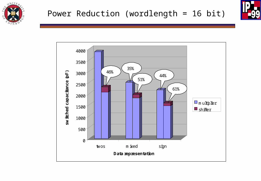
Power Reduction in Multiplier Circuit (wordlength = 16 bit)
47%35%
53%44%
62%
0
500
1000
1500
2000
2500
3000
3500
4000
twos mixed sign
Data representation
multiplier
shifter
swit
ched
cap
acit
ance
(p
F) 46%
35%
51%44%
61%
Power Reduction (wordlength = 16 bit)

Power Reduction at Coefficient Bus (wordlength = 16 bit)
0
50
100
150
200
250
300
350
400
swit
ched
cap
acit
ance
(p
F)
twos mixed sign
Data representation
conventional
segmentation
49%37%
54%
37%
54%

DCT Implementation Scheme

2-D DCT Implementation Approach

Simplified Architecture of the DCT Processor

Conventional Programmable FIR Filter Architecture

TDF with Coefficient Ordering Programmable FIR Filter Architecture

Power Reduction (%)

IP1
tNC
Reset
Load
Clock
DataCoefficient
Output
Of/Uf
Top View of IP1

Block Report for IP1

IP2
tNC
Reset
Load
Clock
DataCoefficient
Output
Of/Uf
Top View of IP2

Block Report for IP2

IP3
tNC
Reset
Load
Clock
DataCoefficient Word
Output
Of/Uf
Top View of IP3

Block Report for IP3

0
2000
4000
6000
8000
10000
12000
14000
16000
Are
a
8-bit 16-bit 24-bit
Wordlength
IP1
IP2
IP3
Area Comparison

Top View of IP4
IP4
tNC
Reset
Load
Clock
DataCoefficient
Output
Of/UfBlock Size

IP5
tNC
Reset
Load
Clock
DataCoefficient Word
Output
Of/Uf
Top View of IP5

Top View of IP6

Case Study: a 34-tap bandpass filter

Area and Power Characteristics for the Example Filter

Conclusions
• A methodology for Low Power Implementation of DSP functions has been presented.
• The methodology has been used to develop a number of IPs.
• Significant reductions in Power is reported.
• Power reduction is achieved in the multiplier and system buses.
• Methodology can be used for prototyping other DSP functions.