Lighting the way in computer design
9
he development of optical interconnect technology us- ing fiber optics in the 1970s was a cornerstone of the modern telecommunication industry. Replacing copper cables with optical fibers provides superior performance in terms of wide data bandwidths, reduced noise, and low loss. It also significantly reduces the cost of communication in terms of dollarshitlkm. Optical interconnects not only provided the in- frastructure critical to the explosive growth of telecommunica- tion that followed, but also paved the way for the information industry to flourish today. For a long time, the early success of optical interconnects in telecommunication, however, did not inspire electronic design- ers to adopt it for computer system designs. In particular, prog- ress in inserting optical components and interconnects into digital systems has been hindered by the relatively high costs of optoelectronic components and module assembly, by the lack of a flexible transmission medium that can be planar processed for board-level applications, and by the lack of a packaging platform that can be used for both optical and electronic devices [ 1). For practical purposes, the cost/performance benefit does not justify CIRCUITS 8 DEVICES JANUARY 1998 8755-3996/98/$10.00 01998 IEEE
Transcript of Lighting the way in computer design

he development of optical interconnect technology us- ing fiber optics in the 1970s was a cornerstone of the modern telecommunication industry. Replacing copper cables with optical fibers provides superior performance
in terms of wide data bandwidths, reduced noise, and low loss. It also significantly reduces the cost of communication in terms of dollarshitlkm. Optical interconnects not only provided the in- frastructure critical to the explosive growth of telecommunica- tion that followed, but also paved the way for the information industry to flourish today.
For a long time, the early success of optical interconnects in telecommunication, however, did not inspire electronic design- ers to adopt it for computer system designs. In particular, prog- ress in inserting optical components and interconnects into digital systems has been hindered by the relatively high costs of optoelectronic components and module assembly, by the lack of a flexible transmission medium that can be planar processed for board-level applications, and by the lack of a packaging platform that can be used for both optical and electronic devices [ 1). For practical purposes, the cost/performance benefit does not justify
CIRCUITS 8 DEVICES JANUARY 1998 8755-3996/98/$10.00 0 1 9 9 8 IEEE

the use of optical technology within a digital computer system at a clock frequency much below 1 GHz.
The situation, however, has markedly changed in recent years because:
+ The rapid advancement of microelectronics technology has increased the chip speed, interconnect complexity, 110 pins, and processing power, with clock speeds now reach- ing -500 MHz and increasing.
+ The use of parallel processors as the prevailing supercom- puting architecture has significantly increased the number of processors in high-performance computing.
+ The exponential growth of network computing and global communication networks such as the Internet have cre- ated significant traffic that demands wideband intercon- nects in local- and wide-area network systems.
The increased complexity required for electrical wiring solu- tions for high-speed, high-density cross-platform interconnects has made such systems more costly. In today's applications, data transfer rates exceeding gigabits per second are common in dis- tributed computing systems, interactive multimedia, high- speed ATM switching, and network communication. A cost- effective, wideband interconnect solution for high-speed data communication between chips, modules, boards, backplanes, cabinets, and processors is critically needed in all these systems.
Recently, significant advances in optical materials, devices, and packaging technologies have made optical interconnects the viable wideband interconnect technology of choice. These enabling technologies are vertical-cavity surface-emitting la- ser (VCSEL) devices and low-cost VCSEL packaging; polymer- based optical waveguide and fiber materials; and low-cost micro-optical components, connectors, and fabrication pro- cesses. Some of these new optoelectronic materials and devices can be handled, processed, and packaged much like IC devices using planar fabrication and batch processing. These processes are key requirements for low-cost, large-volume manufactur-
ecent ~evelQpments Several major R&D programs in the US-sponsored by indus- try, U.S. government agencies (such as DARPA and NET), and joint partnership efforts by a combination of both-have taken place in the last few years in an attempt to develop aviable optical interconnect technology for short-haul data-communication applications. Among these programs, the Optoelectronic Tech- nology Consortium (OETC) [2] was an industrial consortium sponsored by DARPA that was aimed at developing key optical in- terconnect technology for computer applications. OETC repre- sented the first major R&D effort-formed originally by GE (later transferred to Lockheed Martin), ATT, IBM, and Honey- well in 1992-that developed 32-channel parallel optical links operated at 500 Mb/s per channel, with a BER < and an av- erage 0.25 W per channel dissipated power. The link included 32-channel AlGaAs VCSEL arrays, driver arrays, GaAs MESFET receiver arrays, and the fiber ribbon array with MAC I1 connec- tors. This program was credited for early recognition of the sig- nificance of VCSEL devices, and it accelerated the development of VCSEL technology from a laboratory novelty at the beginning of the program to a critical optical component that fulfills all de- sired requirements for short-haul optical communication by the time the program ended in 1995.
The POLO program [3]-consisting of Hewlett-Packard (HP), AMP, Inc., DuPont, SDL, and the University of Southern California (USC), and sponsored jointly by industry and by DARPA-started in 1994 with the aim of reducing the cost of the optoelectronic module technology. It has led to the development of bidirectional 10-channel parallel optical links operated at 1 Gb/s per channel. The Jitney program [4], a joint development effort by IBM and 3M, was a NET-sponsored ATP program to de- velop low-cost parallel optical modules operated at 20 channels at 1 Gb/s per channel. It uses 20-channel VCSEL arrays, CMOS driver ICs, and a 20-channel GaAs MESFET receiver array OEIC. The modules are made of plastic-molded optical couplers to in-
ing. In this article. some ofthi5 recent technical progress is dtscribed with ;1 to- cus on efforts to develop dffordablc op toelectronic pxkdging and intei conn2c.t .. . , ! i i 1 - technologies for board and backplane ap- plications. Discussion includes the de- velopment of VCSEL devices and the related packaging technology that lever- ages the electronic planar fabrication process, passive alignment techniques that could reduce significantly the re- current cost in O/E packaging, planar polymer waveguides that can be used for board and backplane applications for higher density, and high-speed optical interconnects to remove the intercon- i
nett bottlenecks among proc- I . Various optoelectronic interconnect development programs in the U S. and the targeted appli- cations areas The inserts illustrate the differences in requirements for optical interconnect tech-
nologies used in telecommunication and data-communication systems essors in a computer system.
24

DARPA
GE, Honeywell, AMP,
AlliedSignal, Columbia,
UCSD
12194-1 2197
N lST1ATP
IBM, 3M
7194-1 2/96
Sponsor DARPA Motorola ~ DARPA/TRP
Participants GE (LMC), ATT, IBM, HP, AMP, DuPont,
Motorola Honeywell SDL, USC
Aggregate data rate
(Gbis) 16 6 1.5
Total power (W) 10 1.7 < 3
Packaging type
Connector type
Wavelength (nm)
lead frame pin grid array lead frame
MAC II MT MT
VCSEL (850) VCSEL (850) VCSEL (850) 1
VCSEL (850)
Polyguide and polymer waveguides,
butt-coupled
62.5/100 MM
waveauides
VCSEL (850)
butt-coupled
200
Fiber coupling fiber/SiOB Polyguide
molded plastic couplers 45-degree micromirror 45-degree micromirror
terface between VCSEL and large core fibers. OptoBus [ 5 ] is a commercial product developed by Motorola available as bidirec- tional 10-channel transceiver modules operated at 200 Mbls per channel. The POINT [5] program-consisting of GE, Honeywell, AMP, AlliedSignal, the University of California at San Diego (UCSD), and Columbia University-aims at development of af- fordable optoelectronic packaging and interconnect technolo- gies using optical polymers for board and backplane applications.
These programs and their targeted applications areas are il- lustrated in Fig. l. The inserts in the figure show the differences in requirements between the optical interconnect technologies used in the tele- and data-communication systems. Table 1 gives a more detailed summary of some of the major subsystem design characteristics in these programs. As shown in Fig. 1, optical in-
terconnect technologies can be classified broadly into three categories according to the transmission data rate and distance:
+ For long-haul communication over several kilometers (such as telecommunication or wide-area networks), single-mode optic fibers and long wavelength, InGaAsP edge-emitting lasers at 1.3 vm and 1.5 pm are used. Single-channel point-to-point interconnects are typical.
+ For a communication distance in the range of tens to hun- dreds of meters (such as local-area networks, intercon- nects between high-speed servers, workstation clusters, or supercomputers), multimode optic fibers and short wave- length AlGaAs/GaAs semiconductor lasers at 0.85 vm are commonly employed, using either single or multiple chan- nels. Programs like OETC, POLO, OptoBus, and Jitney de- veloped the technologies for these applications.
I Proiect 1 OETC 1 OptoBus 1 POLO
>eriod of development 1 7192-5/95 1 announced 11194 7/94-I 2196
Number of channels 32132 1 011 0 1 Oil 0 module, 12/12
backplane, 144 __ 20120
150 625,1000 500
board, backplane, c 1 1 c 30 I Max link length (m) --! 100 I 30 1-300
40x40 47x47 28x1 8 Module size (pm) 33X44X5 38x38~13
1 3
500
__ 2
25011 00 Channel pitch (mm) 1 140 250 250
lead frame
surface-mount pin grid array
MT ~ 3M connectors TECS fiber
62.51250 MM 62.5/250 MM
Electrical interfaces LVDS, ECL PECL
References [31
CMOS 1 LVDS
CIRCUITS 8 DEVICES JANUARY 1998
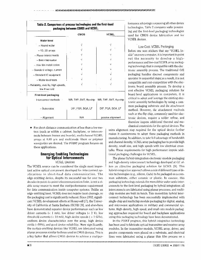
Table 2. Comparison of process technologies and the first-level packaging between CMOS and VCSEL.
Wafer level
- Round wafer
- 1 D, 2D arrays
- Planar interconnects
- Batch fabrication
-Thin film metallization
- Standard voltage, current
-Standard IC equipment
- Wafer-level tests
- Reliability, stability, high speeds,
low threshold
First-level packaging
- Interconnect methods
- Substrates
-Alignment
CMOS
71 4 4
WB, TAP, SMT, flip-chiL
DIP, PGA, BGA, LF
NIA
VCSEL
71 4 4 71 71 i 71 71 4
NB, TAP, SMT, flil
DIP, PGA, BGA,
passive alignmi
+ For short-distance communication of less than a few me- ters (such as within a cabinet, backplane, or intercon- nects between frames and boards), multichannel VCSEL arrays at 0.85 pm and multimode fibers or polymer waveguides are desired. The POINT program focuses on these applications.
Emerging Enabling Technologies for Optical Interconnects
VCSEL Devices The VCSEL source can be considered the single most impor- tant active optical component developed for interconnect ap- p l ica t ions i n s h o r t - h a u l da ta c o m m u n i c a t i o n . The edge-emitting device, despite its successful use for over two decades in point-to-point telecommunication links, is not a vi- able array source to meet the cost/performance requirement for data communication inside computer systems. Unlike an edge-emitting laser, VCSEL does not require facet cleavage, so the packaging cost is significantly reduced. Since 1992, signifi- cant VCSEL development efforts at Honeywell [7], the Univer- sity of California a t Santa Barbara (UCSB) [SI, and elsewhere have demonstrated superior device performances such as low driver currents (< 1 mA), low driver voltages (< 2 V), low threshold currents (< 10 mA), high device speeds ( > 1 GHz), uniform device characteristics over the array, high device yields (-98%), and good device reliability. More significantly, the surface-emitting devices like VCSEL are fabricated using planar processes similar to those used in CMOS devices. This is a key factor that allows CMOS devices to achieve a costiper-
formance advantage surpassing all other device technologies. Table 2 compares wafer process- ing and the first-level packaging technologies used for CMOS device fabrication and for VCSEL devices.
Low-Cost VCSEL Packaging Before one sees stickers that say “VCSEL In- side” on every computer, it is important to point o u t t h e necessi ty t o develop a h i g h - performance and low-cost VCSEL array packag- ing technology that is compatible with the elec- tronic assembly process. The traditional O/E packaging handles discreet components and operates in sequential steps; as a result, it is not compatible and cost-competitive with the elec- tronic board assembly process. To develop a cost-effective VCSEL packaging solution for board-level applications in computers, it is critical to adopt and leverage the existing elec- tronic assembly technologies by using a com- mon packaging substrate and die attachment method. However, die attachment methods such as the flip-chip, commonly used for elec- tronic devices, require a solder reflow, and therefore impose additional thermal and me- chanical constraints for the optical devices. The
extra alignment step required for the optical device further makes it cumbersome to adopt these packaging methods in manufacturing. In addition, to take full advantage of bandwidth and channel density, VCSEL array packaging has to provide high density, small size, and high speeds with low electrical cross- talks. These requirements for high performance impose addi- tional packaging challenges for VCSEL.
The planar hybrid-integration electronic-module packaging and high-density interconnect technology developed at GE of- fers an attractive packaging solution for VCSEL [9]. This hybrid-integration approach allows a mix of different types of de- vice technologies (e.g., silicon, GaAs) to be packaged on a com- mon substrate, either ceramic or plastic. In essence, this packaging technology extends the monolithic wafer-scale inter- connects to the first-level packaging by hybrid integration; all interconnects are fabricated using planar processes, and multi- chip modules are built in batch. This monolithic hybrid inter- connect technology has been successfully implemented with single-chip and multichip module packaging for digital, analog, and microwave applications in military and commercial sys- tems. High-density, high-speed, and small-size module packag- ing approaches required for board and backplane applications using this packaging technology have been demonstrated.
In the POINT program, this hybrid integration technology has been used to fabricate optical transmitter and receiver array modules. In the transmitter module, VCSEL array, driver, and passive components were placed on a substrate, and electrical lines were fabricated using a planar thin film process on a

(a) Fabricate O/E Modules in Frame and Test
(b) Dice into Individual Modules (c) Assemble to Board and Interface to ODtical Wavecluides -
I. A VCSEL packaging technology, developed at GE, that leverages the planar and batch fabrication processes used in the CMOS process to allow (a) fabrication of multiple transmitter modules in a single run and pretest, (b) dicing into single modules, and (c) assembly on a circuit board.
The VCSEL and receiver arrays were designed and fabricated at Honeywell Technology Center.
1 Transmitter Array Receiver Array
I \ MT Connectors /'
PolyguideTM To : Polymer Waveguides Polymer Waveguides Fiber Ribbon
3. Key components in an optical interconnect between a VCSEL transmitter and a receiver unit assembled on the test boards. A test result shows an eye diagram at 1 GHz.
Table 3. UESEL module packaging process flow.
Prepare flex circuit frame
Pick and place VCSEL, drivers, and passive components
Fabricate metal interconnects
Mold plastic substrate
Perform frame-level tests
Dice into individual OiE modules
Prepare for next-level packaging
Interface to optical waveguides
polyimide layer laminated over the de- vices. The electrical lines were fabricated using a copper metallization process that includes resist patterning, sputtering, electroplating, and etching. Electrical lines can be impedance-controlled to the desired value t o minimize reflection noises. Low parasitic capacitance is achieved by replacing wire bonds with thin-film-deposited electrical intercori- nects. The substrate material can be ei- ther ceramic or plastic. In plastic packaging, the VCSEL array is encapsu- lated in a plastic enclosure and attached to a polyimide overlay. Plastic packaging reduces the recurrent packaging cost and is compatible with high-volume produc- tion. The receiver array was built using the same packaging structure and pro- cess. Figure 2 shows the batch process used in the VCSEL assembly that allows multiple VCSEL modules to be built in a single process run. The module can be tested before dicing and final assembly.
The VSCEL module packaging process is shown in Table 3. Fig- ure 3 shows the key components in a test board built for the opti- cal link test. The board includes a VCSEL array transmitter designed and fabricated at Honeywell Technology Center, a r e ceiver array, and a PolyguideTMwaveguide that couples the light output from a VCSEL to a receiver (Polyguide is a trademark of E.I. du Pont de Nemours & Co., Inc.). The waveguide-to- waveguide and waveguide-to-fiber ribbon are connected using MT connectors. The insert in the figure shows an eye diagram of the optical-link tested at 1 GHz [lo]. These results demon- strated, for the first time, the development of a high- performance and high-density packaging platform for simulta- neously handling both optical and electronic components by employing an identical planar-fabrication process.

4. Polymer waveguide inferfaces to VCSEL devices developed a f AMP. (a) A planar waveguide is directly placed and attached to a VCSEL module surface without air gap. (b) A 45-degree facet fabricated at the end o f a Polyguide waveguide for coupling VCSEL output to the waveguide. (c) A short section o f Polyguide waveguide with MT connectors. (d) Coupling tolerance between a VCSEL and a multimode waveguide using this type
o f packaging scheme.
Passive Alignment In an optoelectronic subassembly, the cost associated with those processes related to alignment contribute to a significant part of the subsystem cost. Methods for reducing the O/E packaging cost by minimizing or reducing the alignment steps-such as self-alignment or attaching the optical device onto other subcar- riers using a silicon optical bench (SOB)-have been investi- gated intensively. A low-cost alignment solution for O/E packaging in manufacturing remains a challenge. The mono- lithic hybrid-integration packaging method discussed above provides aplanar module surface, which lends itself to the place- ment and attachment of a planar waveguide like Polyguide di- rectly on top of a transmitter and/or receiver module using passive alignment. Figure 4 shows schematically this kind of waveguide attachment and optical-coupling method between the VCSEL device and the planar waveguide placed directly on top of the VCSEL module. The light output from aVCSEL is cou- pled efficiently to the waveguide via a 45-degree microreflector fabricated at the end of awaveguide. The figure also shows a cou- pling between a VCSEL and waveguide (Fig. 4(a)), a 45-degree micromirror fabricated at thewaveguide end face (Fig. 4(b)), and a short section of Polyguide waveguide connected to an MT con- nector developed at AMP (Fig. 4 (c)). The tolerance between a VCSEL and a multimode waveguide using this kind of coupling scheme is about k25 pm (Fig. 4(d)) [l].
In the POINT program, several passive-alignment tech- niques have been evaluated, including the adaptive placement of alignment pedestals using a pick-and-place machine, laser- trimmed polymer alignment pedestals, fabrication of the pedes- tals using laser-direct patterning of photosensitive polymers, and fabrication of the alignment pedestals directly on the VCSEL chip. A generic passive-alignment process, developed at AMP, uses a high-precision excimer laser system to adaptively mi- cromachine the alignment structures [ 101. In this process, a pre- cision excimer laser micromachine is used to fabricate the alignment wells in the plastic module body, then the precision microspheres were placed inside the wells. Laser micromachin- ing produced an accurate and reproducible process for passive
with - 1 y m accuracy. This kind of accuracy is sufficient for a multimode system in which typical waveguide dimensions are -60 pm, and the alignment tolerance between a VCSEL device and a multimode waveguide is typically about +20 pm for the coupling scheme discussed here.
alignment of an array of polymer waveguides to a VCSEL array
Planar Polymer Waveguide Low-loss silica-based optical fiber and edge-emitting lasers were the key enabling technologies that brought the fiber-optics revo- lution to long-haul telecommunication. A low-loss planar poly- mer waveguide, together with VCSEL array devices, could play a

- - -
- Table 4. Properties of optical polymers investigated under the POINT program.
AlliedSignal Polymers Polyetherimide
NIA ULTEM@
Temperature range -55 "C to > 155 "C
60 PPm
Patternability photo-patterned
Material type
-55 "C to 160 "C -55 "C to 180 "C
-40 ppm 31 ppm (core)
photo-patterned RIE
i
SM, MM waveguides
acrylate
I SM, MM waveguides
couplers, filters SM, MM waveguides
acrylic
board, MCM; backplane,
Optical indices 1.48 to 1.51 1.32 to 1.58 1
board, MCM; backplane, board, fiber-to-device interfaces MCM-to-MCM
ULTEM@ (core)/
core = 1.64
cladding = 1.54
@ 0.85 mm
Optical losses 0.08 dB/cm @J 0.8 pm 0.35 dB/cm @ 1.3 pm
1.6 dB/cm @ 1.55 um
0.02 dB/cm @J 0.85 pm 0.1 dE3icm @ 1.3 pm
0.45 dBicm @ 1.55 um
0.1 dBkm @ 0.85 pm
1.3 dBicm @J 13 pm
Devices
Applications
similar role in bringing optical interconnects to the circuit- board level. Recently, there have been several promising poly- meric materials developed with intrinsic optical losses of 0.1 to 0.2 dB/cm in the near-IR spectral range. Planar optical waveguides fabricated using these polymeric materials have shown a loss of less than 0.2 dB/cm at 0.85 pm. Table 4 summa- rizes polymers investigated under the POINT program and some of their selected properties (111.
Among these polymeric materials, Polyguide waveguide, an acrylate-based polymer developed by DuPont, has shown an ex- cellent layer quality and thickness control [12]. Both single- mode and multimode planar waveguide devices have been fabri- cated using a photolithography and lamination process. Under both the POLO and POINT programs, multichannel waveguides were fabricated using Polyguide waveguides connected to MT- type connectors-a molded plastic miniature connector that has gained popularity as array connectors used in optical inter- connects. MT-type connectors can be used for both fiber and waveguide ribbons, thus providing an ideal interface for waveguide-to-fiber interconnects. Since the waveguides are photo-patterned, the polymer used as an optical medium pro- vides the flexibility for making fan-in and fan-out transitions that cannot be done with the rigid silica fiber.
Another class of acrylate-based polymers has been developed at AlliedSignal. This polymeric material has an optical loss measured at less than 0.1 dB/cm at 0.85 pm. Single-mode waveguide devices of a few micrometers in size, as well as multi- mode waveguides and microstructures of several hundred mi- crometers in size have been fabricated using photopatterning and/or laser-direct writing. This material also has a high con- trast; as a result, structures can be fabricated with steep side
5. Scanning electron micrographs o f AlliedSignal polymeric structures. Clockwise from top left: (a) a laser-fabricated
multimode waveguide terminated by cleaving, (b) a laser-defined multimode guide with a vertical end facet achieved by direct laser
termination, (c) a mask-produced 1 x 2 single-mode power splitter, and (d) a waveguide device pigtailed using AlliedSignal's
fiber gripper technology.
29

T, MT SMT MT R,
High Interconnect Density (I00 km) High Number of Channels (144) Low insertion Loss (1 0.5 dB) Low Crosstalk (<25 dB)
0 Hiqh Speed (1 Gbis) ~ ~~
6. A backplane test structure, developed at AMP, for evaluating high- density interconnects between a transmitter and receiver. There are
144 lines at 100 p m pitch between the two super-MT connectors (SMT), with each of them fanning out to interconnect six MT-type connectors.
walls, which is a useful feature for making waveguide-to-fiber in- terfaces. Figure 5 demonstrates the unique capabilities in this polymer for fabricating a variety of micro-optical structures, de- veloped at AlliedSignal [ 131.
A third type of polymer with low optical loss in IR is polyeth- erimide [14]. This material exhibits low optical losses at 0.85 pm and at 1.3 pm. A commercially available polyetherimide-UL- TEM@ engineering thermoplastic-has excellent temperature and mechanical stability and has been used with excellent dielec- tric properties for printed-circuit boards (ULTEM is a registered trademark of General Electric Company, U.S.A.). The waveguide structure that has been developed jointly by GE and Honeywell uses ULTEM polyetherimide as the core material and benzocy- clobutene (BCB) as the cladding material. Optical waveguides have been developed at Honeywell using RIE with a loss -0.3 dB/cm at 0.85 pm. Using the ULTEMBCB waveguide structure, Honeywell has fabricated multichannel ribbon waveguides on a flexible Kapton substrate and demonstrated optical intercon- nects between two multichip modules (MCMs) at 1 Gb/s data rates separated by about 120 mm [15].
Another potential breakthrough in the area of low-cost poly- meric material for optical interconnects has come from the de- v e l o p m e n t of p las t ic -grade index f ibers w i t h a bandwidth-distance product of 2.5 Gb/s at 100 m. Under DARPA sponsorship, a team that consists of Packard Hughes, Boeing,
7, A high-density optical backplane testbed being constructed at AMP for demonstration o f high-density and high-speed backplane inter-
connects through two 90-degree bends that simulate the bending be- tween a daughterboard and a motherboard.
Boston Optical Fibers, and Honeywell has investigated the speci- fication, design, and production of advanced plastic-fiber-based network components and systems for office networks, commer- cial aircraft, and automobile applications [16]. The advances of plastic optical materials as low-cost transmission media have opened many opportunities for data communication in automo- biles, buildings, and avionics systems in addition to intercom- puter and intracomputer systems.
High-Density Backplane Interconnects As speed, performance, and the number of processors increase, the backplane interconnects between board-to-board and frame-to-frame will become an interconnect bottleneck [ 17, 181. The pyesent state of the art in electrical backplane inter- connects has a pin density of about 100 pins per board-edge inch at a bandwidth of less than 0.5 GHz. However, to minimize the noise voltage in high-speed applications, a signal-to- ground ratio of 1:l is typically required. As a result, the effective pin density is reduced to 50 signal lines per board-edge inch. Deployment of an optical backplane could provide a much higher IiO density.with reduced crosstalk [ 191. Another poten- tial advantage of optical backplane interconnects is the reduc- tion of insertion force because of the elimination of mechanical contacts. In the electrical backplane, the insertion force ex- posed to each 110 pin increases as the pin density increases,
30

and, as a result, an electrical backplane becomes more vulner- able to mechanical failures as the pin density increases.
In the POINT program, AMP has developed a prototype opti- cal backplane structure to demonstrate high-density, high- speed interconnects using polymer waveguides [9]. Figure 6 shows a backplane optical link test structure developed at AMP for evaluation. This test structure has a total of 144 channel mul- timode waveguides with 50-pm cores and 100-pm pitch. This represents an improvement of 5 in interconnect density over the state-of-the-art electrical backplane. At the ends of the test structure, the waveguides are terminated with two super-MT connectors that interconnect a total of 144 waveguide channels. The 144-channel waveguides are then fanned out to 6 MT-type connectors with 24 waveguide channels in each of the MT con- nectors. The preliminary test results have achieved a channel bandwidth close to 1 Gbls over a total distance of 288 mm, and a measured eye diagram is shown in Fig. 6. A high-density back- plane optical link currently under development to interconnect two boards through two right-angle bends for demonstration is shown in Fig. 7.
Conclusion The drastic increase of microprocessor power and speed, the complexity in electrical interconnect solutions, and rapid ad- vances in network computing and global communication have created significant data-communication traffic and communi- cation bottlenecks that demand a low-cost, wideband intercon- nect solution for cross-platform data communication. This article reviewed several major development programs in recent years and discussed a few key enabling technologies that are emerging. A combined market pull and technology push will ac- celerate the development of a low-cost wideband optical inter- connect technology. Like the impact of fiber-optic technology upon telecommunication in the past, we expect that the deploy- ment of optical interconnects to short-haul data communica- tion between circuit boards, frames, backplanes, and intra-boxes will have significant impact upon the computer industry in the coming decades. As the computer and communication tech- nologies converge, we foresee that these two gigantic technolo- gies will be linked together and interconnected by light!
Acknowledgment The author thanks those members of the POINT team who have contributed to the work discussed in this article: R.J. Wojnarowski and W.A. Hennessy of GE Corporate Research and Development, Niskayuna, Ny; J. Rowlette, J. Stack, M. Kadar-Kallen, and E. Green of AMP, Inc., Global Optoelectronic Technology, Harris- burg, PA; Y. Liu and J.P. Bristow of Honeywell Technology Center, Minneapolis, M N and L. Eldada, A. Nahata, and J. Yardley of Al- liedsignal Research 6r TechnoloQy Center, Morristown, NJ. Other development activities not discussed in this paper include the CAD tool development at Columbia University (R.M. Osgood and R. Scarmozzino) and thermal modeling at the University of Cali- fornia at San Diego (S.H. Lee and S. Patra). The author also ac- knowledges the support to the POINT program by DARPNETO (A.
Husain) and the program management provided by USAF Wright Laboratory (J. Grote). Dr. Y.S. Liu is is a Senior Research Scientist in the Electronics Technologies Laboratory at GE Corporate Research and Development in Schenectady, New York, and Program Manager of DARPA’s POINT program (e-mail: [email protected]).
References 1. Y.S. Liu, H.S. Cole, J. Bristow, and Y. Liu, “Hybrid integration of electrical
and optical interconnects,” in OpticalInterconnectII, ed. by R. Chen, Proc. SPIE, 1993. Also, J. Bristow, C . Sullivan, S. Mukherjee, Y. Liu, and A. Hu-. sain, “Progress and status of guided wave optical interconnect technology,” in Optical Interconnects, ed. by R. Chen, vol. 184, Proc. SPIE, pp. 4-10, 1993.
2. Y.M. Wong, D.J. Muehlner, C.C. Faudskar, M. Fishteyn, J.V. Gates, et al., “Technology development of a high density 32-channel 16 Ghps optical data link for optical interconnect applications for the Optoelectronic Tech- nology Consortium (OETC),” Proc. of the IEEE Electronic Components and Technology Conference (ECTC ’96), p. 269, 1996.
3. K.H. Hahn. K. Gibonev. R. Wilson. J. Strazickv. E. Won& et al.. “Giga- bytedsec data communications with the POLO Grallel opt& 1ink;”ECk ’96, p. 301, 1996.
4. J. Crow, J. Choi, M. Cohen, G. Johnson, D. Kuchta, et al., “The Jitney paral- lel optical interconnect,” ECTC ’96, p. 292, 1996.
5. M. Lebby, C.A. Caw, W. Jiang, P.A. Kiely, C.L. Shieh, et al., “Characteristic!: ofVCSEL arrays for parallel optical interconnects,”ECTC ’96, p. 279,1996.
6.Y.S. Liu, R.J. Wojnarowski, W.A. Hennessy, J.P.Bristow,Y.Liu, etal., “Poly- mer optical interconnect technology (POINT),” ECTC ’96, p. 308, 1996.
7. R.A. Morgan, “Advances in vertical cavity surface emitting lasers,” Proc. SPIE, vol. 2147, p. 97, 1994.
8. L.A. Coldren, B.J. Thibeault, “Vertical cavity surface emitting lasers for free space interconnects,” in Optoelectronic Interconnect and Packaging, ed. by R.T. Chen and P.S. Guilfoyle, in Critical Reviews of Optical Science and Technology, SPIE, vol. CR 62, p. 3, 1996.
9. Y.S. Liu, R.J. Wojnarowski, W.A. Hennessy, J.P. Bristow, Y. Liu, “Polymer optical interconnect technology (POINT): Optoelectronic packaging and interconnect for board and backplane applications,” in Optoelectronic In- terconnect andpackaging, ed. by R.T. Chen and P.S. Guilfoyle, SPIE, Criti- cal Review of Optical Sciences and Technology, vol. CR 62, p. 405 1996.
10. Y.S. Liu, R.J. Wojnarowski, W.A. Hennessy, J.P. Bristow, Y. Liu, et al., “High density optical interconnect for board and backplane applications using VCSEL and polymer waveguides,” ECTC ’97, p. 391,1997.
11. Y.S. Liu, H.S. Cole, J.P. Bristow and Y. Liu, “Polymer-based optical inter- connect technology: A route to low-cost optoelectronic packaging and in- terconnect,” in ~Ptical~nterconnec~III, ed. by R. Chen, SPIE, p. 80,1995.
12. B.L. Booth, “Polymer for integrated optical waveguides,” in Polymers for Electronic and Photonic Applications, ed. by C.P. Wong, Academic Press, pp. 549-599, 1993.
13. L. Eldada, L.W. Chacklette, R.A. Nonveek, and J.T. Yardley, “NexL generation optical polymeric photonic devices,” Proc. of the SPIE Annual Meeting, vol. CR 68, p. 207, 1997.
14. H.R. Philipp, D.G. LeGrand, H.S. Co1eandY.S. Liu, “The optical properties of a polyetherimide,” Polymer Engineerinq and Sciences, vol. 29, no. 22, p. 1574, 1989.
15. J. Bristow, “Intra computer optical interconnects: Progress and chal- lenges,” in Optoelectronic Interconnect and Packaging, ed. by R.T. Chen and P.S. Guilfoyle, Critical Reviews of Optical Science and Technology, SPIE, vol. CR 62, p. 318,1996.
16. J. Cirillo, “High speed plastic network Anew technology,”IEEEAESSy~;- temsMagazine, p.10, Oct. 1996.
17. P. Sweazey, “Limits of performance of backplane buses,” in Digital Bus Handbook, ed. by J. De Gaicomo, McGraw-Hill: New York, 1990.
18. R.T. Chen, C. Zhao, and T.€I. Oh, “Performance-optimized optical bi- directional backplane bus for multiprocessor systems,” in Optoelectronic Interconnect and Packaging, ed. by R.T. Chen and P.S. Guilfoyle, SPIE, Critical Reviews of Optical Sciences and Technology, vol. CR 62, p. 299, 1996.
19. Melchior and J.R. Kropp, “A high density optical hackplane connector,” C D l l ECTC ’96, p. 453, 1996.
CIRCUITS 8. DEVICES EZ JANUARY 1998 31