Lecture 9 Multiplexer, Decoder, and PLD
36
Chap 9 C-H 1 Lecture 9 Multiplexer, Decoder, and PLD • SSI (small-scale integration) – NAND, NOR, NOT, flip flop etc • Gate count < 10. • MSI (medium-scale integration) – Adders, multiplexers, decoders, registers, counters • Gate count < 100 • LSI • VLSI (very large-scale integration – Memory chips, microprocessors
Transcript of Lecture 9 Multiplexer, Decoder, and PLD
Chap 9 C-H 1
Lecture 9 Multiplexer,
Decoder, and PLD
• SSI (small-scale integration)
– NAND, NOR, NOT, flip flop etc
• Gate count < 10.
• MSI (medium-scale integration)
– Adders, multiplexers, decoders,
registers, counters
• Gate count < 100
• LSI
• VLSI (very large-scale
integration
– Memory chips, microprocessors
Chap 9 C-H 2
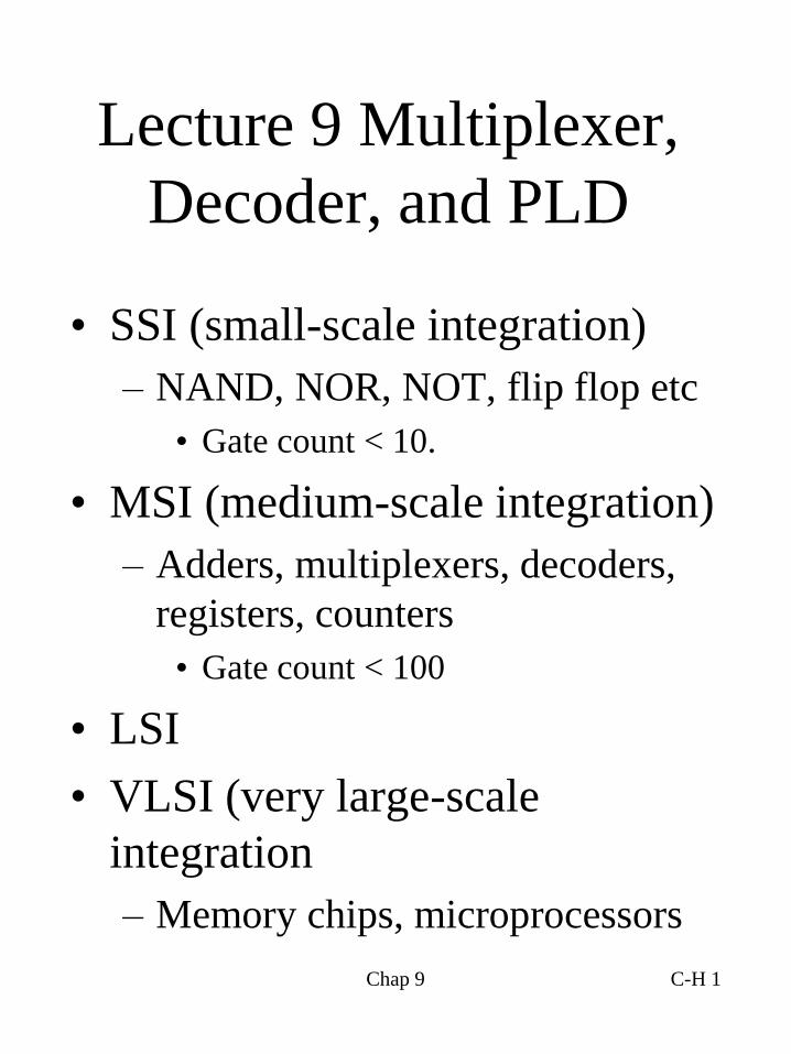
Multiplexers
• Multiplexers are selectors.
Z = A’B’I0 + A’BI1 + AB’I2 + ABI3. (4-
to-1 MUX)
Chap 9 C-H 3
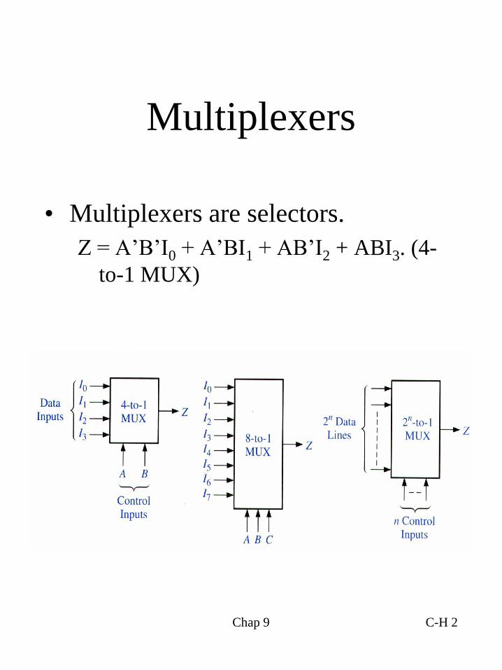
Logic Diagram for MUX
• 8-to-1 MUX

Chap 9 C-H 4
Application of MUX
• Select data.

C-H 5
Application of MUX
Crossbar switch
• As s=0, x1 to
y1, x2 to y2.
• As s=1, x1 to
y2, x2 to y1.
x 1 0
1
x 2 0
1
s
y 1
y 2
x 1
x 2
y 1
y 2
(a) A 2x2 crossbar switch
(b) Implementation using multiplexers
s

Using Mux for logic
function, XOR
• f = w1 xor w2
Chap 9 C-H 6
f
w 1
0
1
0
1
w 2
1
0
0
0
1
1
1
0
1
f w 1
0
w 2
1
0

Better
• Modify the truth table.
• When w1 = 0, f = w2. Otherwise,
f = ~w2
C-H 7
0
1
0
0
1
1
1
0
1
f w 1
0
w 2
1
0
0
1
f w 1
w 2
w 2
f
w 2
w 1

Using Mux to Implement
a barrel shifter
Chap 9 C-H 8

Chap 9 C-H 9
Buffers/Tri-state Buffer
• Driving capability
• High impedance

Chap 9 C-H 10
Tri-state Buffer
Application
• Data transfer between registers

Chap 9 C-H 11
Tri-state Buffer
Application (cont.)
• Source selection

Chap 9 C-H 12
Decoder
• 3-to-8 line decoder
– An n-to-2n decoder generates all 2n
minterms of the n input variables.

Chap 9 C-H 13
More Decoder
• 2-to-4 decoder: minterm
generator

Chap 9 C-H 14
Decoder (cont.)
• 4-to-10 line decoder

Chap 9 C-H 15
ROM
• Read-only memory: stored data can
not be changed under normal
operating conditions.

Chap 9 C-H 16
ROM (cont.)
• ROM size = 2n x m bits.

Chap 9 C-H 17
ROM Basic Structure
• 8-word x 4 bit ROM
– F0 = m0 + m1 + m4 +m6
Chap 9 C-H 18
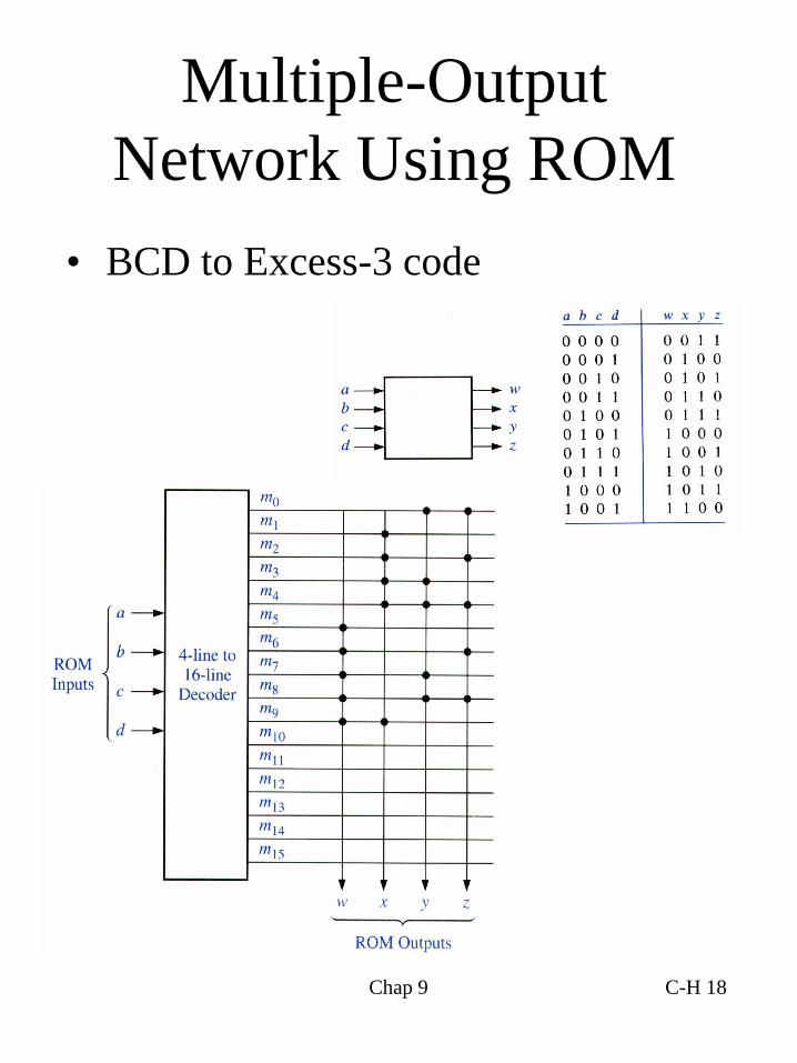
Multiple-Output
Network Using ROM
• BCD to Excess-3 code

Chap 9 C-H 19
Types of ROM
• Mask-programmable ROM
– Contents are stored during
fabrication.
• Field-programmable ROM
– PROM: programmable ROM
• Fusible link (PROM programmer)
– EPROM: erasable PROM
• Use ultraviolet light for erasure.
– EEPROM: electrically erasable
PROM.
• Flash memory
Chap 9 C-H 20
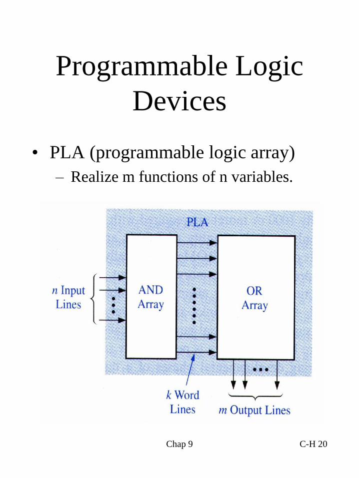
Programmable Logic
Devices
• PLA (programmable logic array)
– Realize m functions of n variables.

Implementation
procedure for PLA
• Prepare the truth table based on your
system
• Write the Boolean expression in SOP (sum
of product) form.
• Obtain the minimum SOP form to reduce
the number of product terms to a minimum.
• Decide the input connection of the AND
matrix for generating the required product
term.
• Then decide the input connections of OR
matrix to generate the sum terms.
• Decide the connections of invert matrix.
• Program the PLA.
Chap 9 C-H 21

Chap 9 C-H 22
Programmable Symbology

Chap 9 C-H 23
PLA
• PLA 3 inputs, 5 product terms, 4
outputs.

Chap 9 C-H 24
PLA
• PLA circuit

Chap 9 C-H 25
PLA (cont.)
• PLA 3 inputs, 5 product terms, 4
outputs. AND-OR array.

Chap 9 C-H 26
PLA Application
• f1 = a’bd + abd + ab’c’ + b’c
• f2 = c + a’bd
• f3 = bc + ab’c’ + abd
• If abcd = 0111, 1st, 5th, 6th rows are
selected. f1 = 1 +0+0, f2 = 1+1+0, etc.

Chap 9 C-H 27
Programmable Array
Logic (PAL) • AND array is programmable. OR
array is fixed.
• Use input buffer to drive many
ANDs.
Input buffer

Chap 9 C-H 28
Programmable Array
Logic (PAL)
• Full Adder using a PAL

Why prefers PLA rather
than ROM
• A combinational circuit may occasionally
have don't-care conditions. When
implemented with a ROM, a don't care
condition becomes an address input that
will never occur.
• The words at the don't care address need
not be programmed and may be left in their
original state(all 0's or all 1's ).
• The has the result that all the bit patterns
available in ROM are used, but for the
don’t care addresses you really can do
without them.
Chap 9 C-H 29

What Programmable
Means
• "programmable" does not indicate that all
PLAs are field-programmable.
• Many are mask-programmed during
manufacture in the same manner as a mask
ROM.
– This is particularly true of PLAs that are
embedded in more complex and numerous
integrated circuits such as microprocessors.
• PLAs that can be programmed after
manufacture are called FPGA (Field-
programmable gate array)
Chap 9 C-H 30

Chap 9 C-H 31
Complex Programming
Logic Devices • Xilinx XCR3064XL CPLD
– Function block (16 macrocells)= PLA
– Macrocell = a flip flop + multiplexers
– IA routes signals
Input of function block
Chap 9 C-H 32
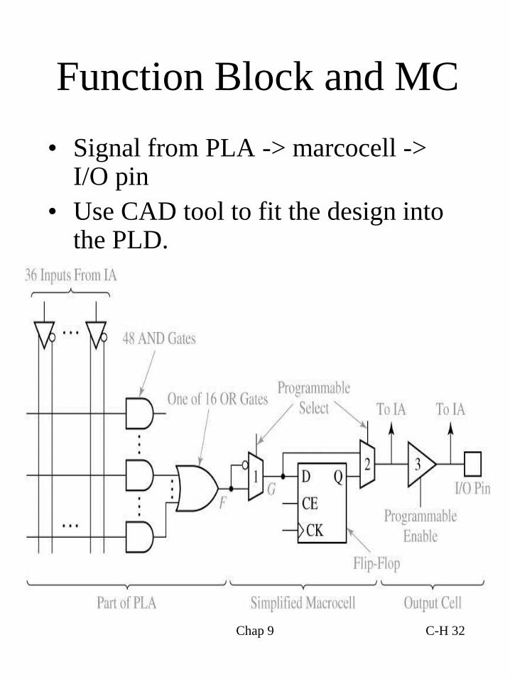
Function Block and MC
• Signal from PLA -> marcocell -> I/O pin
• Use CAD tool to fit the design into the PLD.

Chap 9 C-H 33
Field Programmable
Gate Arrays (FPGA) • Logic cell: configurable logic blocks
(CLBs)
• Input/Output blocks (I/O blocks)

Chap 9 C-H 34
Configurable Logic
Block • Inside a CLB: function generators (LUT),
FFs, and MUXs
• LUT: lookup table (truth table) is a
reprogrammable ROM (16 1-bit words)

Chap 9 C-H 35
A Lookup Table (LUT)
• If we want F = abc (one minterm)
– 1110 (and F=1) + 1111 (and F=1)
• Or if we want F = a’b’c’d’ + a’b’cd’ + …abcd. (15 minterms)
• Require a single function generator. Program the LUT table to get what we want.
a b c d F
0 0 0 0 0
0 0 0 1 1
0 0 1 0 1
…..
1 1 1 1 1
This is a 4-variable function
generator.
Bit stored in the LUT.
To be implemented

Chap 9 C-H 36
Shannon’s Expansion
Theorem • What if # of variables > 4 variables
f (x1, x2,… xn)
= xi’ f (x1, x2,..xi-1, 0, xi+1, … xn) +
xi f (x1, x2,..xi-1, 1, xi+1, … xn)
= xi’ f0 + xif1
f (a, b, c, d, e) = a’ f(0, b, c, d, e) + a f(1, b, c, d, e)
2-1 MUX F = a’I1 + a I2
Let a = 0, what lefts
are terms with b, c, d, e