
Rev. 0.00 4-Channel A/V Decoder with Multiplexer/VGA/LCD ... · TW2851 4-Channel A/V Decoder with...
380
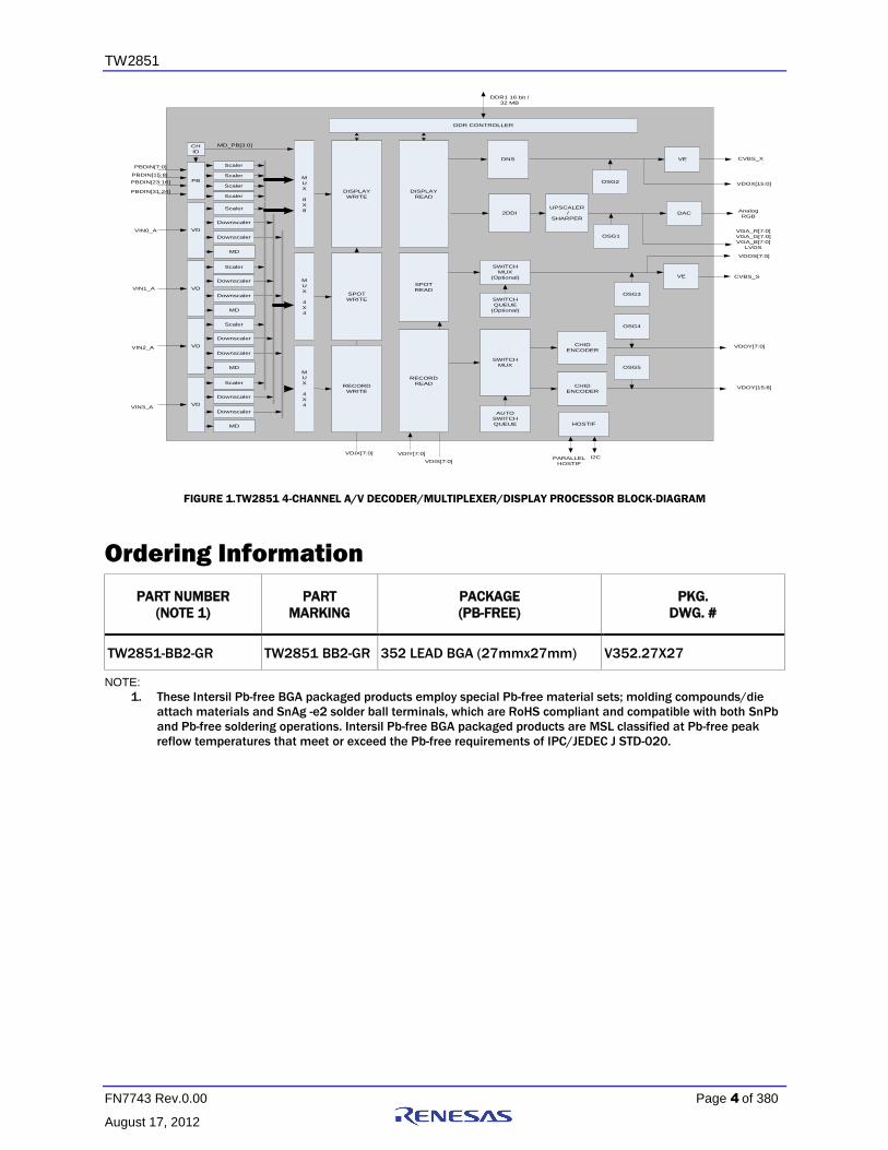
TW2851 4-Channel A/V Decoder with Multiplexer/VGA/LCD Display Processor for Security Applications FN7743 Rev.0.00 Page 1 of 380 August 17, 2012 FN7743 Rev. 0.00 August 17, 2012 DATASHEET The TW2851 is a fully integrated A/V decoder, multiplexer, and display processor chip. It has eight CVBS analog inputs fed into four internal high quality NTSC/PAL video decoders. It has four digital input ports supporting various type of input format, including four BT 656 inputs, two BT 601 inputs, or one 1120 playback input. It has one optional VGA display controller or LCD panel controller, two CVBS display, one digital SPOT output, two digital recorder outputs, and one digital display output. Every output has its associated graphic overlay function that displays bitmap for OSG, single box, 2D array box, borders, privacy mask, and mouse cursor. The four built-in video decoders include four anti- aliasing filters, 10bit Analog-to-Digital converters, proprietary digital gain/clamp controller, and high quality Y/C separator to reduce cross-noise. Associated with each video decoder, there are built- in motion, blind, and night detectors to provide alarm signals, a noise reducer to reduce the impulse noise, and 3 sets of downscalers to provide proper video size into the display, record, and SPOT multiplexers. The TW2851 MUX function selects video inputs from any video decoder/ digital inputs to any of recording / SPOT / VGA display / CVBS display outputs flexibly. The recording multiplexer supports frame / field and byte-interleaved multi-channel video streams in the format of BT 656, BT 1120 to interface with external video compression CODEC. The frame / field allocation of each channel can be flexibly configurable in the multi-channel video stream. The multi-channel video stream features built-in channel ID to identify channels of interest for the CODEC or playback module to properly de- multiplex the multi-channel stream into single channel streams. The motion / night / blind detection information are also embedded as part of the channel ID. The display multiplexer displays up to 8 video windows, with 4 for video decoders and 4 for either digital interface or video decoder interface to support pseudo 8 channel inputs. The location and size of each of the 8 display windows are flexibly configurable. The multiplexed display video is sent to both VGA / LCD and the CVBS output simultaneously. Before the VGA / LCD output, there is a 2D de-interlacer converting the interlaced video into progressive for any PC monitor / LCD panel with resolution up to WXGA+ (1440x900) resolution. The VGA interface provides RGB component with both analog output through 3 embedded DACs and digital TTL outputs. The LVDS interface provides single or dual channel output to drive various TFT LCD panels. The SPOT multiplexer functions as a either SPOT display or a secondary record mux. It supports single D1 frame rate output. When used as display purpose, it is capable of supporting 1 / 4 windows in a fixed configuration. When used as record mux purpose, it is capable of supporting quad window or frame / field interleave multi-channel stream in single D1 frame rate. There are two built-in video encoders features two 10-bit embedded DACs to provide 2 CVBS outputs. The two video encoders are flexibly configurable to output any two of the display, SPOT and record path video content. The TW2851 also includes an audio CODEC with five audio Analog-to-Digital converters and one Digital-to-Analog converter. A built-in audio multiplexer generates digital outputs for recording / mixing and accepts digital input for playback. TW2851 features a cascade function to allow up to 4 TW2851 chips to connect together to increase the total number of channels / windows supported in VGA display and SPOT display. With 4 chips cascaded together, the VGA display path can display up to 32 display windows, and the SPOT display can display up to 16 windows. Analog Video Decoder 4 sets of video decoder accept all NTSC(M/N/4.43) / PAL (B/D/G/H/I/K/L/M/N/60) standards with auto detection 8 CVBS analog inputs for pseudo 8 channel support Integrated video analog anti-aliasing filters and 10 bit CMOS ADCs for each video decoder
Transcript of Rev. 0.00 4-Channel A/V Decoder with Multiplexer/VGA/LCD ... · TW2851 4-Channel A/V Decoder with...

TW2851
4-Channel A/V Decoder with Multiplexer/VGA/LCD
Display Processor for Security Applications
FN7743 Rev.0.00 Page 1 of 380
August 17, 2012
FN7743
Rev. 0.00
August 17, 2012
DATASHEET
The TW2851 is a fully integrated A/V decoder,
multiplexer, and display processor chip. It has eight
CVBS analog inputs fed into four internal high
quality NTSC/PAL video decoders. It has four digital
input ports supporting various type of input format,
including four BT 656 inputs, two BT 601 inputs, or
one 1120 playback input. It has one optional VGA
display controller or LCD panel controller, two CVBS
display, one digital SPOT output, two digital
recorder outputs, and one digital display output.
Every output has its associated graphic overlay
function that displays bitmap for OSG, single box,
2D array box, borders, privacy mask, and mouse
cursor.
The four built-in video decoders include four anti-
aliasing filters, 10bit Analog-to-Digital converters,
proprietary digital gain/clamp controller, and high
quality Y/C separator to reduce cross-noise.
Associated with each video decoder, there are built-
in motion, blind, and night detectors to provide
alarm signals, a noise reducer to reduce the
impulse noise, and 3 sets of downscalers to
provide proper video size into the display, record,
and SPOT multiplexers.
The TW2851 MUX function selects video inputs
from any video decoder/ digital inputs to any of
recording / SPOT / VGA display / CVBS display
outputs flexibly. The recording multiplexer supports
frame / field and byte-interleaved multi-channel
video streams in the format of BT 656, BT 1120 to
interface with external video compression CODEC.
The frame / field allocation of each channel can be
flexibly configurable in the multi-channel video
stream. The multi-channel video stream features
built-in channel ID to identify channels of interest
for the CODEC or playback module to properly de-
multiplex the multi-channel stream into single
channel streams. The motion / night / blind
detection information are also embedded as part of
the channel ID.
The display multiplexer displays up to 8 video
windows, with 4 for video decoders and 4 for either
digital interface or video decoder interface to
support pseudo 8 channel inputs. The location and
size of each of the 8 display windows are flexibly
configurable. The multiplexed display video is sent
to both VGA / LCD and the CVBS output
simultaneously. Before the VGA / LCD output, there
is a 2D de-interlacer converting the interlaced video
into progressive for any PC monitor / LCD panel
with resolution up to WXGA+ (1440x900)
resolution. The VGA interface provides RGB
component with both analog output through 3
embedded DACs and digital TTL outputs. The LVDS
interface provides single or dual channel output to
drive various TFT LCD panels.
The SPOT multiplexer functions as a either SPOT
display or a secondary record mux. It supports
single D1 frame rate output. When used as display
purpose, it is capable of supporting 1 / 4 windows
in a fixed configuration. When used as record mux
purpose, it is capable of supporting quad window or
frame / field interleave multi-channel stream in
single D1 frame rate.
There are two built-in video encoders features two
10-bit embedded DACs to provide 2 CVBS outputs.
The two video encoders are flexibly configurable to
output any two of the display, SPOT and record path
video content.
The TW2851 also includes an audio CODEC with
five audio Analog-to-Digital converters and one
Digital-to-Analog converter. A built-in audio
multiplexer generates digital outputs for recording /
mixing and accepts digital input for playback.
TW2851 features a cascade function to allow up to
4 TW2851 chips to connect together to increase the
total number of channels / windows supported in
VGA display and SPOT display. With 4 chips
cascaded together, the VGA display path can
display up to 32 display windows, and the SPOT
display can display up to 16 windows.
Analog Video Decoder
4 sets of video decoder accept all
NTSC(M/N/4.43) / PAL
(B/D/G/H/I/K/L/M/N/60) standards with auto
detection
8 CVBS analog inputs for pseudo 8 channel
support
Integrated video analog anti-aliasing filters and 10
bit CMOS ADCs for each video decoder

TW2851
FN7743 Rev.0.00 Page 2 of 380
August 17, 2012
High performance adaptive 4H comb filters for all
NTSC/PAL standards
IF compensation filter for improvement of color
demodulation
Color Transient Improvement (CTI)
Automatic white peak control
Programmable hue, saturation, contrast,
brightness and sharpness
Proprietary fast video locking system for non-real-
time application
Noise Reduction to remove impulse noise
Triple high performance scalers scale video input
independently for each of display, recording and
SPOT path
Four built-in motion detectors with 16 X 12 cells,
four blind and night detectors
Digital Input Ports
Supports up to 4 BT. 656 ports, 2 BT. 601, 1 port
RGB, or 1 port BT. 1120. The BT 1120 supports a
54 MHz channel with 4 D1 put together.
Auto cropping / strobe for playback input using 2
built-in Analog / Digital Channel ID decoder for
selecting 4 out of maximum of 16 channels from
multi-channel input stream
4 built-in down scalers for displaying arbitrary size
windows on the display output
Analog/Digital VGA Display
Native Resolution of VGA, D1, SVGA, XGA, up to
WXGA+ (1440x900), capable of displaying 4 D1
screens side by side without downscaling.
Up-Scaler for ZOOM function and playback of full
screen D1 image
3 Built-in DACs for analog VGA RGB output
Digital RGB interface in 24-bit TTL output
DDC channel interface to read the external
monitor configuration
Built-in 2D De-interlacer for progressive output
Sharpness control with horizontal/vertical peaking
Black/White Stretch
Programmable hue, brightness, saturation,
contrast
Independent RGB gain and offset controls
Programmable Gamma correction for each of
RGB
Built-in 2-layer 9-window bitmap OSG with 16-bit
per pixel color
Hardware OSG bitmap up-scaler to allow same
content displayed on both VGA/LCD and CVBS
output
Additional OSG layers such as window border box,
2D motion box, Privacy Mask overlay, and Mouse
Cursor support
TFT LCD Panel Support
Supports panel with similar resolution as the VGA
port
Supports single or dual channel LVDS panel
Supports Panel power sequencing.
Supports DPMS for monitor power management
Display CVBS Output
Display Output through one of the two built-in
CVBS video encoder
Built-in 2-layer 9-windows bitmap OSG with 16-bit
per pixel color
Additional OSG layers such as window border box,
2D motion box, mouse cursor, and Privacy Mask
overlay
Display Multiplexer
Displays 8 windows for 4 video decoder inputs
plus 4 digital input channels or 8 video decoder
channels to support pseudo 8-channel
Either Live or Strobe capture mode for pseudo 8-
channel support
Horizontal / Vertical mirroring for each window
Last field / frame image captured when video-loss
detected
Simultaneous output to both VGA/LCD and CVBS
output with the same video content
Record Multiplexer
2 ports of BT. 656, 1 port BT. 601, or 1 port of
BT.1120-like digital Interface support up to 4 D1
real-time recording output to external CODEC
Supports Frame/Field Interleaved mode with 8
picture types or byte interleaved stream for multi-
channel video output
Either Live or Strobe capture mode for pseudo 8-
channel support
Supports dynamic field / frame picture-type and
channel allocation through a switching queue up
to 2048 entries
Horizontal / Vertical mirroring for each window
2 Built-in channel ID encoder carrying channel and
motion / blind / night detection information of
each field/frame in multi-channel stream

TW2851
FN7743 Rev.0.00 Page 3 of 380
August 17, 2012
Two built-in 8-window bitmap OSG with 16-bit per
pixel color for each of the two record output ports
Field switching capable OSG supports 4 different
contents changing from field to field through
switching queue
Additional OSG layers such Privacy Mask overlay,
and Mouse Cursor
SPOT Multiplexer
Optionally configured as network output mode
through a BT. 656 digital interface to support
frame/field interleave feature similar to record
path Switch mode
SPOT analog output configurable through one of
the two built-in CVBS video encoder
LIVE capture mode in FULL D1, Quad CIF and 16
QCIF windows
Strobe capture mode for pseudo 8-channel
support
Video window arrangement independent of the
recording and display output
Horizontal and Vertical Mirroring for each channel
Built-in 8 windows bitmap OSGs with 16-bit per
pixel color
Additional OSG layers such as window border box,
Privacy Mask overlay, and Mouse Cursor support
Dual Video Encoders
Flexibly shared by Display, Record and SPOT
Analog NTSC/PAL standards
Programmable bandwidth of luminance and
chrominance signal for each path
Two 10-bit video CMOS DACs
Cascade Capability
VGA display cascade mode displays up to 32
windows (16 video input and 16 playback input)
on both VGA/LCD and CVBS output using 4
TW2851 chips
SPOT display cascade support up to 16 channels
at the D1 output
Built-in 8 windows bitmap OSG with 16-bit per
pixel color
Additional OSG layers such as window border box,
2D motion box, mouse cursor, and Privacy Mask
overlay
Audio CODEC
Integrated five audio ADCs and one audio DAC
providing multi-channel audio mixed analog
output
Supports a standard I2S interface for record
output and playback input
PCM 8/16 bit and u-Law/A-Law 8bit for audio
word length
Programmable audio sample rate that covers
popular frequencies of 8/16/32/44.1/48kHz
External DDR SDRAM
Single centralized external DDR SDRAM of 256
Mb (32 MB) capacity
16-bit wide data bus running at 166 MHz
Auto-refresh
Host Interface
MCU parallel interface with 8 / 16 bits data bus
and 8 /12-bit address bus for higher MCU
interface throughput
Supports both address / data separate or
multiplexed mode
Burst write for faster OSG bitmap upload
Serial I2C interface
PS2 mouse port support
System Clock
Single 27 MHz external crystal clock input
3 built-in PLLs for internal clock generation
Package
352 BGA
TW2851
FN7743 Rev.0.00 Page 4 of 380
August 17, 2012
VD
Scaler
Downscaler
PB
Scaler
Scaler
Scaler
Scaler
CH
ID
PBDIN[7:0]
VIN0_A
Downscaler
VIN1_A
VIN2_A
VIN3_A
M
U
X
8
X
8
MD
VD
Scaler
Downscaler
Downscaler
MD
VD
Scaler
Downscaler
Downscaler
MD
VD
Scaler
Downscaler
Downscaler
MD
MD_PB[3:0]
M
U
X
4
X
4
M
U
X
4
X
4
DISPLAY
WRITE
DDR CONTROLLER
DISPLAY
READ
SPOT
READ
RECORD
WRITE
SPOT
WRITE
VDIX[7:0] VDIY[7:0]
2DDI
UPSCALER
/
SHARPER
DAC
OSG1
VE
OSG3
VE
AUTO
SWITCH
QUEUE
SWITCH
MUX OSG5
VDOY[7:0]
VDOX[15:0]
OSG4
VDOY[15:8]
CVBS_X
Analog
RGB
DDR1 16 bit /
32 MB
SWITCH
MUX
(Optional) CVBS_S
SWITCH
QUEUE
(Optional)
VDOS[7:0]
HOSTIF
PARALLEL
HOSTIF
I2C
PBDIN[15:8]
CHID
ENCODER
CHID
ENCODER
DNS
OSG2PBDIN[23:16]
PBDIN[31:24]
VDIS[7:0]
RECORD
READ
VGA_R[7:0]
VGA_G[7:0]
VGA_B[7:0]
LVDS
FIGURE 1. TW2851 4-CHANNEL A/V DECODER/MULTIPLEXER/DISPLAY PROCESSOR BLOCK-DIAGRAM
Ordering Information
PART NUMBER
(NOTE 1)
PART
MARKING
PACKAGE
(PB-FREE)
PKG.
DWG. #
TW2851-BB2-GR TW2851 BB2-GR 352 LEAD BGA (27mmx27mm) V352.27X27
NOTE:
1. These Intersil Pb-free BGA packaged products employ special Pb-free material sets; molding compounds/die
attach materials and SnAg -e2 solder ball terminals, which are RoHS compliant and compatible with both SnPb
and Pb-free soldering operations. Intersil Pb-free BGA packaged products are MSL classified at Pb-free peak
reflow temperatures that meet or exceed the Pb-free requirements of IPC/JEDEC J STD-020.

TW2851
FN7743 Rev.0.00 Page 5 of 380
August 17, 2012
Table of Contents Analog Video Decoder ........................................................................... 1 Digital Input Ports.................................................................................... 2 Analog/Digital VGA Display .................................................................. 2 TFT LCD Panel Support ........................................................................ 2 Display CVBS Output ............................................................................. 2 Display Multiplexer ................................................................................. 2 Record Multiplexer.................................................................................. 2 SPOT Multiplexer .................................................................................... 3 Dual Video Encoders ............................................................................. 3 Cascade Capability ................................................................................. 3 Audio CODEC .......................................................................................... 3 External DDR SDRAM ............................................................................ 3 Host Interface ........................................................................................... 3 System Clock ........................................................................................... 3 Package .................................................................................................... 3
Ordering Information ...................................................................... 4 Table of Contents ............................................................................ 5 Table of Figures ............................................................................... 7 Table List .......................................................................................... 9 Pin Diagram .................................................................................... 10
TW2851 (352 BGA) ............................................................................... 10 Pin Descriptions ............................................................................ 11
Analog Interface .................................................................................... 11 Digital VGA / LVDS Interface............................................................... 12 Host Interface ......................................................................................... 14 Audio Digital Interface .......................................................................... 15 Digital Input Interface ........................................................................... 16 Digital Output Interface ........................................................................ 17 DDR SDRAM Interface ......................................................................... 18 Misc Interface ......................................................................................... 19 Power / Ground Interface .................................................................... 20
Functional Description ................................................................. 22 CVBS Video Input ................................................................................. 23
Formats ............................................................................................... 23 Analog Front-End ............................................................................... 23 Decimation Filter ................................................................................. 24 AGC and Clamping ............................................................................ 24 Sync Processing ................................................................................. 25 Y/C Separation ................................................................................... 25 Color Decoding ................................................................................... 25 Chrominance Processing .................................................................. 27 Luminance Processing ...................................................................... 27 Pseudo 8 Channels ............................................................................ 28 Cropping Function .............................................................................. 28 Noise Reduction ................................................................................. 29 Downscalers ....................................................................................... 29 Motion Detection ................................................................................. 29 Blind Detection .................................................................................... 33 Night Detection ................................................................................... 34
Digital Video Input ................................................................................. 34 ITU-R BT. 656 Digital Video Input Format........................................ 34 ITU-R BT. 601 Digital Video Input Format........................................ 36 ITU-R BT. 1120 Digital Video Input Format ..................................... 36 Multi-Channel Video Format.............................................................. 36 Playback Input Channel De-multiplexer ........................................... 38 Channel ID Decoder .......................................................................... 40 Cropping and Scaling Function ......................................................... 40
Video Multiplexers ................................................................................ 41 Capture Control .................................................................................. 41 Read Control ....................................................................................... 43 Window Configuration ........................................................................ 46 Video Window Control ....................................................................... 46 Image Enhancement Processing ..................................................... 47
Video Output .......................................................................................... 49 Analog VGA/RGB Video Output ....................................................... 49 CVBS Video Output ........................................................................... 49 Digital Output ....................................................................................... 53 TFT Panel Support ............................................................................. 56
Video Cascade....................................................................................... 56
Display Path ........................................................................................ 57 SPOT Path .......................................................................................... 57
Channel ID .............................................................................................. 59 Channel ID Types ............................................................................... 59 Channel ID Encoding Setting ............................................................ 61 Channel ID Decoding Setting ............................................................ 62 Digital Channel ID Format .................................................................. 63
OSG .......................................................................................................... 66 Video Border Layer............................................................................. 66 2-Dimensional Arrayed Box ............................................................... 67 Bitmap Layer ....................................................................................... 68 Single Box ........................................................................................... 71 Mouse Pointer ..................................................................................... 71
Audio Codec .......................................................................................... 73 Audio Clock Master/Slave mode ....................................................... 74 Audio Detection ................................................................................... 75 Audio Multi-Chip Cascade ................................................................. 75 Serial Audio Interface ......................................................................... 78 Audio Clock Slave Mode Data Output Timing ................................. 81 ACLKP/ASYNP Slave Mode Data Output Timing .......................... 82 Audio Clock Generation ..................................................................... 84 Audio Clock Auto Setup ..................................................................... 86
Host Interface ......................................................................................... 87 Serial Interface .................................................................................... 89 Parallel Interface ................................................................................. 90 VGA DDC I2C Master Interface ........................................................ 93 PS2 Mouse Interface .......................................................................... 94 Interrupt Interface ................................................................................ 94 Burst Interface to DDR SDRAM ........................................................ 94
External DRAM Interface ..................................................................... 95 Chip Reset / Initiation ............................................................................ 95 Frequency Synthesizer Setup ............................................................ 96
Register Description By Function ............................................... 97 CVBS Video Input ................................................................................. 97
Video Decoder .................................................................................... 97 Internal Pattern Generator ............................................................... 120 Noise Reduction ............................................................................... 121 Downscaler ....................................................................................... 123 Motion / Blind / Night Detection ........................................................ 126
Digital Input Interface .......................................................................... 131 656 / 601 / RGB Port ........................................................................ 131 CHID Decode / Strobe ..................................................................... 136 Playback Cropping ........................................................................... 144 Playback Downscalers ..................................................................... 146
Video Multiplexers .............................................................................. 147 Record Control .................................................................................. 147 Record Switch Queue ...................................................................... 150 Record CHID Encoder ..................................................................... 152 Display Control .................................................................................. 154 SPOT Control ................................................................................... 161 SPOT Switch Queue........................................................................ 164 SPOT CHID Encoder....................................................................... 166
Display CVBS Processing ................................................................ 169 Down-Scaling .................................................................................... 169
Display VGA / LCD Processing ........................................................ 171 Up-Scaling ......................................................................................... 174 Gamma Table ................................................................................... 175 2D De-interlace ................................................................................. 175 Image Enhancement........................................................................ 176
Video Output ........................................................................................ 179 Record CVBS Timing....................................................................... 179 SPOT CVBS Timing ........................................................................ 180 Display CVBS Timing ....................................................................... 181 CVBS Encoder Control .................................................................... 183 Display Cascade Timing .................................................................. 186 Display VGA Timing ......................................................................... 189 TFT Panel Control ............................................................................ 190
OSG ........................................................................................................ 194 OSG Bitmap Write / Move ............................................................... 194
TW2851
FN7743 Rev.0.00 Page 6 of 380
August 17, 2012
OSD Bitmap Read ........................................................................... 198 1D Box Control ................................................................................. 203 2D Box Control ................................................................................. 208 Cursor Control ................................................................................... 213
Audio CODEC ...................................................................................... 214 Host Interface ....................................................................................... 227
VGA DDC Interface Control ............................................................ 227 PS2 Mouse Interface Control .......................................................... 229 Interrupt .............................................................................................. 230 DDR Burst ......................................................................................... 231
DDR Memory Controller .................................................................... 232 Misc Control ......................................................................................... 234
Register Description By Address.............................................. 240 Page 0: 0x000 ~ 0x0FE ....................................................................... 240 Page 1: 0x100 ~ 0x1FE ....................................................................... 275
Page 2: 0x200 ~ 0x2FE ....................................................................... 292 Page 3: 0x300 ~ 0x3FE ....................................................................... 323 Page 4: 0x400 ~ 0x4FE ....................................................................... 328 Page 5: 0x500 ~ 0x51F ....................................................................... 340 Page 6: 0x600 ~ 0x620, 0x640 ~ 0x65F, 0x690 ~ 0x6FE............... 343 Page 9: 0x9C0 ~ 0x9DF ...................................................................... 353 Page M: 0xM21 ~ 0xM3F, 0xM60 ~ 0xM8F, where M = 5 ~ 9 ...... 355 Page E : 0xE00 ~ 0xEFE .................................................................... 367
AC Timing ..................................................................................... 373 Parametric Information ............................................................... 376
AC/DC Electrical Parameters ............................................................ 376 Package Outline Drawing ........................................................... 379 Life Support Policy ...................................................................... 380 Revision History .......................................................................... 380
TW2851
FN7743 Rev.0.00 Page 7 of 380
August 17, 2012
Table of Figures Figure 1. TW2851 4-Channel A/V Decoder/Multiplexer/Display Processor Block Diagram ........................................................ 4 Figure 2. TW2851 Pin Diagram (Bottom View) ............................................................................................................................ 10 Figure 3. TW2851 front-end modules .......................................................................................................................................... 22 Figure 4. The frequency response of the video input anti-aliasing filter.................................................................................... 24 Figure 5. The characteristic of Decimation Filter ....................................................................................................................... 24 Figure 6. The characteristics of Luminance Notch Filter for NTSC and PAL ............................................................................ 26 Figure 7. The characteristics of Chrominance Band-Pass Filter for NTSC and PAL................................................................ 26 Figure 8. The characteristics of Chrominance Low-Pass Filter Curves .................................................................................... 27 Figure 9. The Characteristic of Luminance Peaking filter .......................................................................................................... 28 Figure 10. Motion mask and Detection Cell ................................................................................................................................. 31 Figure 11. The relationship between current and reference field when MD_REFFLD = “0” ..................................................... 32 Figure 12. The relationship between current and reference field when MD_REFFLD = “1” ..................................................... 33 Figure 13. Timing diagram of ITU-R BT. 656 format .................................................................................................................... 35 Figure 14. The VSYNC/HSYNC Timing in BT. 601 Interface ........................................................................................................ 36 Figure 15. Multi-channel Picture Types supported by TW2851 .................................................................................................. 37 Figure 16. Playback Input De-multiplexer .................................................................................................................................... 39 Figure 17. Block diagram of video controller ............................................................................................................................... 41 Figure 18. The sequence to change display window configuration ........................................................................................... 46 Figure 19. The video output block diagram ................................................................................................................................. 49 Figure 20. Horizontal and vertical timing control ........................................................................................................................ 51 Figure 21. Characteristics of luminance filter ............................................................................................................................. 52 Figure 22. Characteristics of chrominance Filter ....................................................................................................................... 52 Figure 23. Example of reconstruction filter ................................................................................................................................ 53 Figure 24 TW2851 Cascade in Display / SPOT paths .................................................................................................................. 56 Figure 25. Cascade in Display path only ...................................................................................................................................... 57 Figure 26. The example of auto channel ID for various record output formats ........................................................................ 61 Figure 27. The related registers for channel ID encoding .......................................................................................................... 62 Figure 28. The related registers for channel ID decoding .......................................................................................................... 62 Figure 29. The illustration of the Motion digital channel ID in VBI period................................................................................. 64 Figure 30. The illustration of the AUTO/DETECTION/USER digital channel ID in VBI period .................................................. 65 Figure 31. The overlay priority of OSG layers ............................................................................................................................. 66 Figure 32. The 2D arrayed box in table mode and motion display mode ................................................................................... 68 Figure 33. Block Diagram of Audio Codec ................................................................................................................................... 73 Figure 34. Audio Decimation Filter Response ............................................................................................................................ 74 Figure 35. Recommended Clock Master cascade mode system with ACLKRMASTER = 1; ASYNROEN = 0; PB_MASTER=076 Figure 36. Recommended Clock Slave Sync Slave cascade mode system with ACLKRMASTER=0; ASYNROEN=1;
PB_MASTER=0 ................................................................................................................................... 77 Figure 37. Timing Chart of Serial Audio Interface ...................................................................................................................... 78 Figure 38. Timing Chart of Multi-channel Audio Record ............................................................................................................ 79 Figure 39. Audio Record Falling Edge Triggered Input/Output Timing, ACLKMASTER=0, RM_SYNC=0 ............................... 81 Figure 40. Audio Record Falling Edge Triggered Input/Output Timing, ACLKMASTER=0, RM_SYNC=1 ............................... 81 Figure 41. Audio Record Rising Edge Triggered Input Timing, ACLKMASTER=0, RM_SYNC=0, ASTBROEN=1 .................... 81 Figure 42. Audio Record Rising Edge Triggered Input Timing, ACLKMASTER=0, RM_SYNC=1, ASTBROEN=1 .................... 82 Figure 43. Audio Playback Falling Edge Triggered Input Timing, RM_SYNC=0, PB_MASTER=0, ADATPDLY=0 ................... 82 Figure 44. Audio Playback Falling Edge Triggered Input Timing, RM_SYNC=1, PB_MASTER=0, ADATPDLY=0 ................... 82 Figure 45. Audio Playback Falling Edge Triggered Input Timing, RM_SYNC=0, PB_MASTER=0, ADATPDLY=1 ................... 82 Figure 46. Audio Playback Falling Edge Triggered Input Timing, RM_SYNC=1, PB_MASTER=0, ADATPDLY=1 ................... 83 Figure 47. Audio Playback Rising Edge Triggered Input Timing, RM_SYNC=0, PB_MASTER=0, ADATPDLY=1 .................... 83 Figure 48. Audio Playback Rising Edge Triggered Input Timing, RM_SYNC=1, PB_MASTER=0, ADATPDLY=1 .................... 83 Figure 49. Audio Playback Rising Edge Triggered Input Timing, RM_SYNC=0, PB_MASTER=0, ADATPDLY=0 .................... 83 Figure 50. Audio Playback Rising Edge Triggered Input Timing, RM_SYNC=1, PB_MASTER=0, ADATPDLY=0 .................... 84 Figure 51. The serial interface for the case of slave address. (Read : “0x085”, Write : “0x084”) ............................................. 89

TW2851
FN7743 Rev.0.00 Page 8 of 380
August 17, 2012
Figure 52. Write timing of serial interface .................................................................................................................................... 89 Figure 53. Read timing of serial interface .................................................................................................................................... 89 Figure 54. Write timing of parallel interface with address/data multiplexing mode ................................................................. 90 Figure 55. Read timing of parallel interface with address / data multiplexing mode................................................................ 90 Figure 56. Write timing of parallel interface with separate address / data bus ......................................................................... 91 Figure 57. Read timing of parallel interface with separate address / data bus ......................................................................... 92 Figure 58. The window ID of the 16 window configuration .......................................................................................................168 Figure 59. Cascade Interface Timing Diagram ...........................................................................................................................374 Figure 60. Playback Interface Timing Diagram ..........................................................................................................................375 Figure 61. Digital Video Output Timing Diagram .......................................................................................................................376

TW2851
FN7743 Rev.0.00 Page 9 of 380
August 17, 2012
Table List Table 1. Video Input Formats Supported by the TW2851................................................................ 23 Table 2. ITU-R BT.656 SAV and EAV code sequence ...................................................................... 35 Table 3. Playback Input Configurations ........................................................................................... 38 Table 4. Capture Modes support of display/SPOT/record paths .................................................... 42 Table 5. Display Channel Configuration .......................................................................................... 43 Table 6. Switch Queue Entry Definition of Record Path ................................................................. 45 Table 7. Switch Quene Entry Definition of SPOT Path .................................................................... 45 Table 8. Analog output video standards .......................................................................................... 50 Table 9. Digital Record Output Port Configuration ......................................................................... 54 Table 10. ITU-R BT.656 SAV and EAV code sequence ...................................................................... 55 Table 11. SP_CC_EN Setting for the Record Path Cascade ............................................................. 58 Table 12. The Detection channel ID information ............................................................................... 59 Table 13. Auto channel ID Byte 0 through Byte 3 (For 4 regions) .................................................... 60 Table 14. The Picture Type Code........................................................................................................ 60 Table 15. Sequence of Multi-channel Audio Record ......................................................................... 80 Table 16. Audio frequency 256xfs mode: AIN5MD = 0, AFS384 = 0 ..................................................... 85 Table 17. Audio frequency 320xfs mode: AIN5MD = 1, AFS384 = 0, 44.1/48 KHz not supported ...... 85 Table 18. Audio frequency 384xfs mode: AIN5MD = 0, AFS384 = 1, 44.1/48 KHz not supported ...... 86 Table 19. Pin assignments for serial and parallel interface .............................................................. 87 Table 20. Timing parameters of parallel interface with address / data multiplexing mode ............ 91 Table 21. Timing parameters of parallel interface with separate address / data bus ...................... 92 Table 22. Cascade Clock Timing Parameters .................................................................................. 373 Table 23. Playback Interface Timing Parameters ............................................................................ 374 Table 24. Digital Video Output Timing Parameters ......................................................................... 376 Table 25. Characteristics .................................................................................................................. 376
TW2851
FN7743 Rev.0.00 Page 10 of 380
August 17, 2012
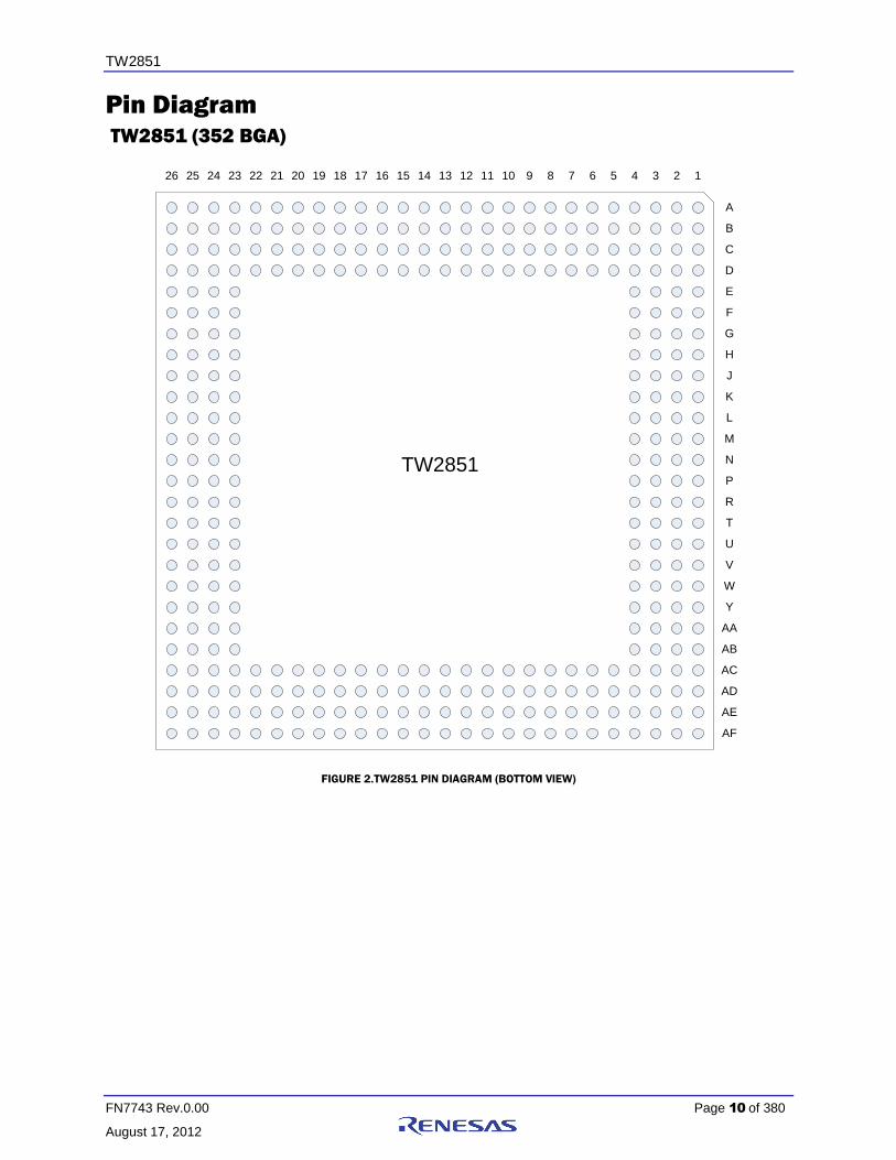
Pin Diagram
TW2851 (352 BGA)
TW2851
1234567891011121314151617181920212223242526
A
B
C
D
E
F
G
H
J
K
L
M
N
P
R
T
U
V
W
Y
AA
AB
AC
AD
AE
AF
FIGURE 2. TW2851 PIN DIAGRAM (BOTTOM VIEW)

TW2851
FN7743 Rev.0.00 Page 11 of 380
August 17, 2012
Pin Descriptions
Analog Interface
NAME PIN # TYPE DESCRIPTION
VIN1A M2 A Composite video input A of channel 1.
VIN1B M3 A Composite video input B of channel 1.
VIN2A N2 A Composite video input A of channel 2.
VIN2B N3 A Composite video input A of channel 2.
VIN3A P2 A Composite video input A of channel 3.
VIN3B P3 A Composite video input B of channel 3.
VIN4A R2 A Composite video input A of channel 4.
VIN4B R3 A Composite video input B of channel 4.
AIN1 U2 A Audio input of channel 1.
AIN2 U3 A Audio input of channel 2.
AIN3 V1 A Audio input of channel 3.
AIN4 V2 A Audio input of channel 4.
AIN5 V3 A Audio input of channel 5.
AINN T3 A AINN
AOUT T2 A Audio mixing output.
VAOX W2 A Display CVBS analog video output.
VAOS W3 A SPOT CVBS analog video output.
VAOXR AA2 A Display output R signal
VAOXG AA3 A Display output G signal
VAOXB AB2 A Display output B signal
RTERM Y4 A R Termination

TW2851
FN7743 Rev.0.00 Page 12 of 380
August 17, 2012
Digital VGA / LVDS Interface
NAME
PIN #
TYPE DESCRIPTION
VGA LCD
VGA_VS AF2 n/a O
VSYNC for VGA output
This pin is also used as a power up strap pin to
to determine the data bus width of the parallel host
interface.
Pull Up: 16 bit mode, Pull Down: 8 bit mode
VGA_HS AE2 n/a O HSYNC for VGA output
VGA_DE AD2 n/a I/O Data Enable bit for VGA / RGB data output
VGA_CLK AF1 n/a I/O Clock output for VDOUTX (27, 54, or up to
106.25 MHz)
DDC_CLK AC3 n/a O
DDC channel clock
Output low active, otherwise tri-state
Need external pull up
DDC_DATA AC2 n/a I/O
DDC channel data
Output low active, otherwise tri-state
Need external pull up
MPP_VDO /
VDOX [15:8] /
VGA_B[7:0]
AD7, AC8, AD8, AC9,
AD9, AC10, AD10,
AD11
O
When register 0xEC0 bit [5] is set to 0, these pins
are used as VDOX[15:8]. Otherwise these pins
Are used as VGA B component output.
VDOX[15:8] is used as display data output in 601
Format as Y component for driving external VGA/
de-interlacer chips. Depending on the display
Resolution, these signals are running from 27MH
to 110 MHz
LVDS_A0B /
VGA_R[0] AE14 O
Negative differential LVDS 0th channel data output
or VGA Red Color Bit 0
LVDS_A0 /
VGA_R[1] AF14 O
Positive differential LVDS 0th channel data output
or VGA Red Color Bit 1
LVDS_A1B /
VGA_R[2] AE13 O
Negative differential LVDS 1st channel data output
or VGA Red Color Bit 2
LVDS_A1 /
VGA_R[3] AF13 O
Positive differential LVDS 1st channel data output
or VGA Red Color Bit 3
LVDS_A2B /
VGA_R[4] AE12 O
Negative differential LVDS 2nd channel data output
or VGA Red Color Bit 4

TW2851
FN7743 Rev.0.00 Page 13 of 380
August 17, 2012
NAME
PIN #
TYPE DESCRIPTION
VGA LCD
LVDS_A2 /
VGA_R[5] AF12 O
Positive differential LVDS 2nd channel data output
or VGA Red Color Bit 5
LVDS_CK0B n/a AE11 O Negative differential LVDS 0th though 3rd channel clock
output
LVDS_CK0 n/a AF11 O Positive differential LVDS 0th though 3rd channel clock
output
LVDS_A3B
VGA_R[6] AE10 O
Negative differential LVDS 3rd channel data output
or VGA Red Color Bit 6
LVDS_A3 /
VGA_R[7] AF10 O
Positive differential LVDS 3rd channel data output
or VGA Red Color Bit 7
LVDS_A4B /
VGA_G[0] AE9 O
Negative differential LVDS 4th channel data output
or VGA Green Color Bit 0
LVDS_A4 /
VGA_G[1] AF9 O
Positive differential LVDS 4th channel data output
or VGA Green Color Bit 1
LVDS_A5B /
VGA_G[2] AE8 O
Negative differential LVDS 5th channel data output
or VGA Green Color Bit 2
LVDS_A5 /
VGA_G[3] AF8 O
Positive differential LVDS 5th channel data output
or VGA Green Color Bit 3
LVDS_A6B /
VGA_G[4] AF7 O
Negative differential LVDS 6th channel data output
or VGA Green Color Bit 4
LVDS_A6 /
VGA_G[5] AE7 O
Positive differential LVDS 6th channel data output
or VGA Green Color Bit 5
LVDS_CK1B n/a AF6 O Negative differential LVDS 4th though 7th channel clock
output
LVDS_CK1 n/a AE6 O Positive differential LVDS 4th though 7th channel clock
output
LVDS_A7B /
VGA_G[6] AF5 O
Negative differential LVDS 7th channel data output
or VGA Green Color Bit 6
LVDS_A7 /
VGA_G[7] AE5 O
Positive differential LVDS 7th channel data output
or VGA Green Color Bit 7
FPPWC n/a AD3 O Power on/off control for flat panel display
FPBIAS n/a AE3 O Panel bias control
FPPWM n/a AF3 O PWM control for panel backlight
TW2851
FN7743 Rev.0.00 Page 14 of 380
August 17, 2012
Host Interface
NAME PIN# TYPE DESCRIPTION
HSP[1:0] B16, D20 I
Host Interface Configuration
00: Address / Data Mux, with ALE high active
01: I2C interface
10: Address / Data Mux, with ALE low active
11: Address Data separate, with 12 bit address
HCSB E24 I Parallel Interface: Chip Select signal
Serial Interface: Slave address bit 0
HALE / SCLK D23 I
Address line enable for parallel interface.
Serial clock for serial interface /
Clock for I2C Bus
HRDB C21 I Read enable for parallel interface.
VSSO for serial interface.
HWRB D25 I Write enable for parallel interface.
VSSO for serial interface.
HDAT[6:0] A24, C25, B25, A25,
C26, B26, A26 I/O
Parallel Interface: Data bus bit 6:0
Serial Interface: HDAT[6:1] is slave address bit 6:1
HDAT[7] / SDAT B24 I/O Parallel Interface: Data bus bit 7
Serial Interface: Data bit for I2C bus
HDAT[15:8] B21, A21, B22, A22,
B23, A23, D24, C24 I/O
Data bus for parallel interface used in
16-bit data bus mode
HADDR[11:0]
C17, B17, A17, C18,
B18, A18, C19, B19,
A19, C20, B20, A20
I The Host Address Bus in Address / Data Separate
Mode (HSP == 3’b11)
HWAITB E25 O
Wait signal to the external MCU.
This signal is low active, and tri-state otherwise.
Needs external pull-up resister.
IRQ C16 O
Interrupt request signal. This signal is low active,
and tri-state otherwise. Needs external pull-up
resistor.
PS2_CK E26 I/O
PS2 mouse interface clock signal
Output low active, otherwise tri-state.
Need external pull up
PS2_D D26 I/O
PS2 Mouse Interface data signal
Output low active, otherwise tri-state.
Need external pull up
TW2851
FN7743 Rev.0.00 Page 15 of 380
August 17, 2012
Audio Digital Interface
NAME PIN# TYPE DESCRIPTION
ACLKR AC26 I/O Audio I2S serial clock input/output of record
ASYNR AD24 I/O Audio I2S serial sync input/output of record
ADATR AB25 O Audio I2S serial data output of record
ADATM AD25 O Audio I2S serial data output of mixing
ACLKP AD26 I/O Audio I2S serial clock input/output of playback.
ASYNP AC24 I/O Audio I2S serial sync input/output of playback.
ADATP AB26 I Audio I2S serial data input of playback.
ALINKO AC25 O Link signal for multi-chip connection serial output
ALINKI D13 I Link signal for multi-chip connection serial input
TW2851
FN7743 Rev.0.00 Page 16 of 380
August 17, 2012
Digital Input Interface
NAME PIN # TYPE DESCRIPTION
PB0_DIN[7:0] B2, C3, B3, A3,
C4, B4, A4, D5 I
Video data of playback port 0 input in BT. 656,
Video data of playback port 0 input in BT. 601,
or Video data of playback port 0 input in RGB
PB0_CLK A2 I Clock of playback input BT 656 port 0
PB1_DIN[7:0] C2, D2, E2, D3,
E3, D4, E4, F4 I
Video data of playback port 1 input in BT. 656,
Video data of playback port 0 input in BT. 601,
or Video data of playback port 0 input in RGB
PB1_CLK E1 I Clock of playback input BT 656 port 1
PB2_DIN[7:0] H3, H2, G3, G2,
G1, F3, F2, F1 I
Video data of playback port 2 input in BT. 656,
Video data of playback port 1 input in BT. 601,
or Video data of playback port 0 input in RGB
PB2_CLK H1 I Clock of playback input BT 656 port 2
PB3_DIN[7:0] L3, L2, K3, K2,
K1, J3, J2, J1 I
Video data of playback port 3 input in BT. 656,
Video data of playback port 1 input in BT. 601
PB3_CLK L1 I Clock of playback input BT 656 port 3
PB0_VS B1 I Playback VSYNC for 601 port 0
PB0_HS A1 I Playback HSYNC for 601 port 0
PB1_VS C1 I Playback VSYNC for 601 port 1
PB1_HS D1 I Playback HSYNC for 601 port 1

TW2851
FN7743 Rev.0.00 Page 17 of 380
August 17, 2012
Digital Output Interface
NAME PIN# TYPE DESCRIPTION
VDOX[7:0]
AC12, AD12, AD13,
AC14, AD14, AD15,
AE15, AF15
O
VDOX[7:0] is used as display data output in 656 or 601 output
as U/V components for use as cascade output, or used to drive
external VGA/de-interlacer chips. Depending on display output
resolution, these signals are running from 27 MHz up to 110 MHz
max
CLKOX AD16 O CLKOX is used as display clock output
VDIX[7:0] C5, B5, A5, B6, A6,
C7, B7,A7 I Lower 8 bits of display path cascade input
CLKIX C6 I Display path clock input
VDOY [7:0]
AD19, AC19, AF20,
AE20, AC20, AF21,
AE21, AF22
O Digital video data output for record path in BT. 656 port 1, or U/V
of BT. 601.
VDOY[15:8]
AF16, AE16, AF17,
AE17, AF18, AE18,
AC18, AF19
O Digital video data output for record path in
BT. 656 port 2 or Y of BT 601.
CLKOY
(CLKOY0) AC21 O Clock output for record path (27, 54 or 108 MHz)
CLKOYB
(CLKOY1) AE19 O
Clock output for record path 1 (27, 54 or 108 MHz) or the Reverse
Clock Output for record path. The CLKOYB signal can be set to the
reverse of CLKOY with adjustable delay used for byte interleave
record output sampling.
HSOY AE22 O HSYNC output if the record output is in ITU-R BT.
601 format
VSOY AD21 O VSYNC output if the record output is in ITU-R BT. 601 format
VDIY[7:0] C8, B8, A8, C9,
B9, A9, B10, A10 I Lower 8 bits of record path cascade input
CLKIY D9 I Record path clock input
VDOS[7:0]
AD22,AC22,AF23,
AE23, AF24, AE24,
AF25, AE25
O Digital video data output for SPOT/Network Port
CLKOS AF26 O Clock of the SPOT/network output port
VDIS[7:0]
B11, A11, B12,
A12, C13, B13, A13,
B14
I SPOT path cascade data input
CLKIS C11 I SPOT path cascade clock input

TW2851
FN7743 Rev.0.00 Page 18 of 380
August 17, 2012
DDR SDRAM Interface
NAME PIN# TYPE DESCRIPTION
DQ[15:0]
F26, F25, F24, G26,
G24, H26, H24, J26,
K26, K24, L26, L25,
L24, M26, M25, M24
I/O DDR DRAM data bus.
ADDR[12:0]
U26, U25, U24, V26,
V25, V24, W26,
W24, Y26, Y25, Y24,
AA26, AA24
O DDR DRAM address bus
DQS[1:0] H25, K25 I/O DDR DRAM Data Strobe
DM[1:0] J24, N24 O Byte Mask
BA1 T26 O DDR DRAM bank1 selection.
BA0 T24 O DDR DRAM bank0 selection.
RASB R26 O DDR DRAM row address selection.
CASB R25 O DDR DRAM column address selection.
WEB P25 O DDR DRAM write enable.
MCLK P26 O DDR DRAM Clock Output
MCLKB N26 O DDR DRAM Clock Output
CKE P24 O Clock Enable
TW2851
FN7743 Rev.0.00 Page 19 of 380
August 17, 2012
Misc Interface
NAME PIN# TYPE DESCRIPTION
EXT_PCLK A16 I/O EXT_PCLK pin is used for internal testing only.
This pin should be left open
EXT_MCLK A14 I/O EXT_MCLK pin is used for internal testing only.
This pin should be left open
XTI (27 MHz) B15 I Crystal (27 MHz) Clock Input
XTO A15 O Crystal Clock Output
TP1 C15 I/O Test Pin 1. For internal testing only. This pin should
be left open.
TEST_EN J4 I Test mode enable. For internal use only.
Normally tied to 0
RSTB AB3 I System reset. Active low.
TW2851
FN7743 Rev.0.00 Page 20 of 380
August 17, 2012
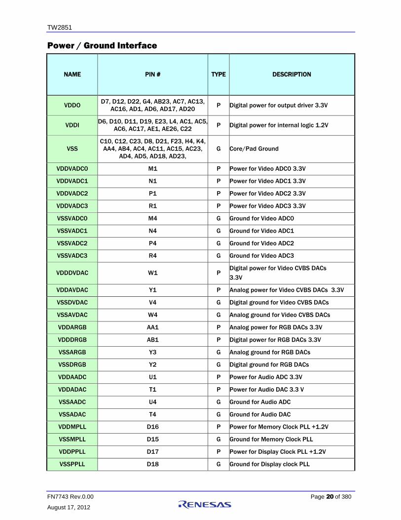
Power / Ground Interface
NAME PIN # TYPE DESCRIPTION
VDDO D7, D12, D22, G4, AB23, AC7, AC13,
AC16, AD1, AD6, AD17, AD20 P Digital power for output driver 3.3V
VDDI D6, D10, D11, D19, E23, L4, AC1, AC5,
AC6, AC17, AE1, AE26, C22 P Digital power for internal logic 1.2V
VSS
C10, C12, C23, D8, D21, F23, H4, K4,
AA4, AB4, AC4, AC11, AC15, AC23,
AD4, AD5, AD18, AD23,
G Core/Pad Ground
VDDVADC0 M1 P Power for Video ADC0 3.3V
VDDVADC1 N1 P Power for Video ADC1 3.3V
VDDVADC2 P1 P Power for Video ADC2 3.3V
VDDVADC3 R1 P Power for Video ADC3 3.3V
VSSVADC0 M4 G Ground for Video ADC0
VSSVADC1 N4 G Ground for Video ADC1
VSSVADC2 P4 G Ground for Video ADC2
VSSVADC3 R4 G Ground for Video ADC3
VDDDVDAC W1 P Digital power for Video CVBS DACs
3.3V
VDDAVDAC Y1 P Analog power for Video CVBS DACs 3.3V
VSSDVDAC V4 G Digital ground for Video CVBS DACs
VSSAVDAC W4 G Analog ground for Video CVBS DACs
VDDARGB AA1 P Analog power for RGB DACs 3.3V
VDDDRGB AB1 P Digital power for RGB DACs 3.3V
VSSARGB Y3 G Analog ground for RGB DACs
VSSDRGB Y2 G Digital ground for RGB DACs
VDDAADC U1 P Power for Audio ADC 3.3V
VDDADAC T1 P Power for Audio DAC 3.3 V
VSSAADC U4 G Ground for Audio ADC
VSSADAC T4 G Ground for Audio DAC
VDDMPLL D16 P Power for Memory Clock PLL +1.2V
VSSMPLL D15 G Ground for Memory Clock PLL
VDDPPLL D17 P Power for Display Clock PLL +1.2V
VSSPPLL D18 G Ground for Display clock PLL
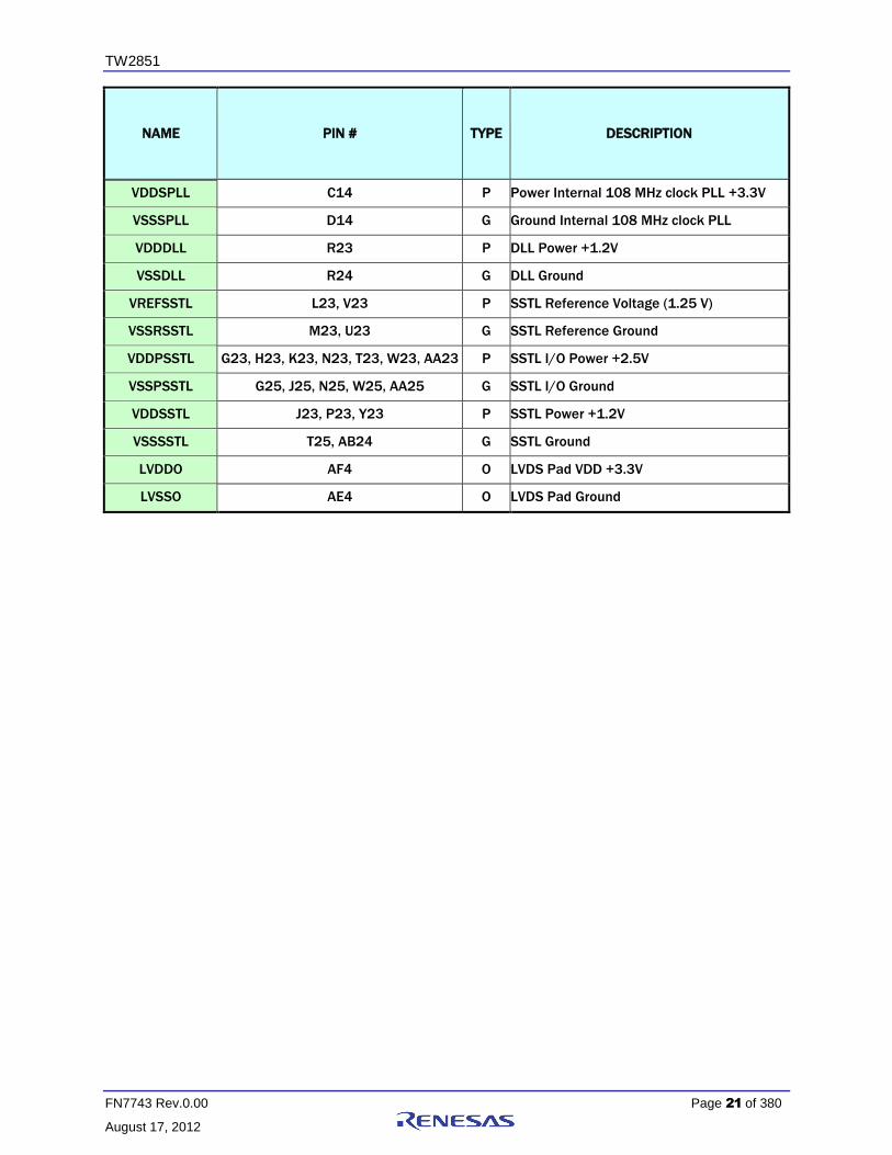
TW2851
FN7743 Rev.0.00 Page 21 of 380
August 17, 2012
NAME PIN # TYPE DESCRIPTION
VDDSPLL C14 P Power Internal 108 MHz clock PLL +3.3V
VSSSPLL D14 G Ground Internal 108 MHz clock PLL
VDDDLL R23 P DLL Power +1.2V
VSSDLL R24 G DLL Ground
VREFSSTL L23, V23 P SSTL Reference Voltage (1.25 V)
VSSRSSTL M23, U23 G SSTL Reference Ground
VDDPSSTL G23, H23, K23, N23, T23, W23, AA23 P SSTL I/O Power +2.5V
VSSPSSTL G25, J25, N25, W25, AA25 G SSTL I/O Ground
VDDSSTL J23, P23, Y23 P SSTL Power +1.2V
VSSSSTL T25, AB24 G SSTL Ground
LVDDO AF4 O LVDS Pad VDD +3.3V
LVSSO AE4 O LVDS Pad Ground

TW2851
FN7743 Rev.0.00 Page 22 of 380
August 17, 2012
Functional Description The TW2851 has 12 input interfaces consisting of 8 analog composite video inputs and 4 digital video inputs.
The 8 analog video inputs go through 4 analog multiplexers to select 4 out of 8 video inputs to feed to the 4
built-in video decoders. The video decoders feature with 10-bit ADC and luminance/chrominance processor
to convert the analog video signal into digital video streams. The four digital inputs for playback application
are decoded by internal ITU-R BT656, ITU-R BT601, Component RGB, or ITU-R BT1120 decoders, through the
channel ID decoder, and fed to display multiplexer. When using the BT 1120, the playback interface is
capable of supporting 4 D1 pictures in one single port.
VIDEO
DECODER
M
U
X
VIN0A
VIN0B
Noise
Reduction
SCALER
Motion Detection
SCALER
SCALER
VIN0X
VIN0Y
VIN0S
MV0
VIDEO
DECODER
M
U
X
VIN1A
VIN1B
Noise
Reduction
SCALER
Motion Detection
SCALER
SCALER
VIN1X
VIN1Y
VIN1S
MV1
VIDEO
DECODER
M
U
X
VIN2A
VIN2B
Noise
Reduction
SCALER
Motion Detection
SCALER
SCALER
VIN2X
VIN2Y
VIN2S
MV2
VIDEO
DECODER
M
U
X
VIN3A
VIN3B
Noise
Reduction
SCALER
Motion Detection
SCALER
SCALER
VIN3X
VIN3Y
VIN3S
MV3
4D1 Byte
Interleave
Output
BT 656 /
BT 601 /
BT 1120
Decoder
PB_IN0
PB_IN1
PB_IN2
PB_IN3
CHID
Decoder
CROP /
SCALER
CROP /
SCALER
CROP /
SCALER
CROP /
SCALER
PB3X
PB2X
PB1X
PB0X
MVPB0
MVPB1
MVPB2
MVPB3
FIGURE 3. TW2851 FRONT-END MODULES
Each built-in video decoder has one motion detector, one noise reduction processor, and three scalers – one
for the display path, one for the SPOT path, and one for the record path. The digital video input has four
scalers, one for each of the four de-multiplexed video channels. The video input front-end module is shown in
Figure 3.

TW2851
FN7743 Rev.0.00 Page 23 of 380
August 17, 2012
CVBS Video Input
FORMATS
The TW2851 has build-in automatic standard discrimination circuitry. The circuit uses burst-phase, burst-
frequency and frame rate to identify NTSC, PAL or SECAM color signals. The standards that can be identified
are NTSC (M), NTSC (4.43), PAL (B, D, G, H, I), PAL (M), PAL (N), PAL (60) and SECAM (M). Each standard can
be included or excluded in the standard recognition process by software control. The exceptions are the base
standard NTSC and PAL, which are always enabled. The identified standard is indicated by the Standard
Selection (SDT) register. Automatic standard detection can be overridden by software controlled standard
selection.
TW2851 supports all common video formats as shown in Table 1.
TABLE 1. VIDEO INPUT FORMATS SUPPORTED BY THE TW2851
FORMAT LINES FIELDS FSC COUNTRY
NTSC-M 525 60 3.579545 MHz U.S., many others
NTSC-Japan (1) 525 60 3.579545 MHz Japan
PAL-B, G, N 625 50 4.433619 MHz Many
PAL-D 625 50 4.433619 MHz China
PAL-H 625 50 4.433619 MHz Belgium
PAL-I 625 50 4.433619 MHz Great Britain, others
PAL-M 525 60 3.575612 MHz Brazil
PAL-CN 625 50 3.582056 MHz Argentina
SECAM 625 50 4.406MHz 4.250MHz France, Eastern Europe, Middle
East, Russia
PAL-60 525 60 4.433619 MHz China
NTSC (4.43) 525 60 4.433619 MHz Transcoding
NOTE:
2. NTSC-Japan has 0 IRE setup.
The analog front-end converts analog video signals to the required digital format. There are total of 4 analog
front-end channels. Every channel contains analog anti-aliasing filter, clamping circuit and 10-bit ADCs. It
allows the support of CVBS input signals. Every channel contains the analog clamping circuit, variable gain
amplifier and high speed ADCs. It allows three separate inputs to be connected simultaneously. A built-in line
locked PLL is used to generate the sampling clock for various inputs.
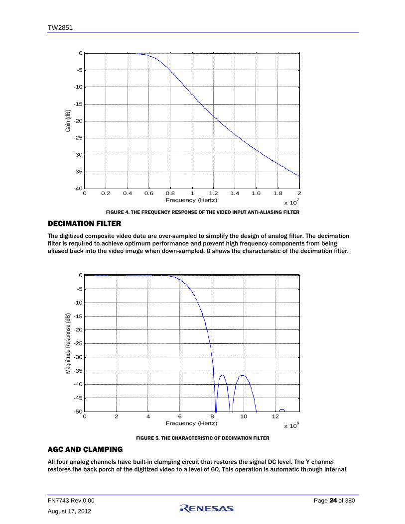
ANALOG FRONT-END
The TW2851 contains four 10-bit ADC (Analog to Digital Converters) to digitize the analog video inputs. The
ADC can be put into power-down mode by the V_ADC_PD (0xEC4) register. The TW2851 also contains an
anti-aliasing filter to prevent out-of-band frequency in analog video input signal. Therefore, there is no need
for external components in the analog input pin except for an AC coupling capacitor and termination resistor.
0 shows the frequency response of the anti-aliasing filter.
TW2851
FN7743 Rev.0.00 Page 24 of 380
August 17, 2012
FIGURE 4. THE FREQUENCY RESPONSE OF THE VIDEO INPUT ANTI-ALIASING FILTER
DECIMATION FILTER
The digitized composite video data are over-sampled to simplify the design of analog filter. The decimation
filter is required to achieve optimum performance and prevent high frequency components from being
aliased back into the video image when down-sampled. 0 shows the characteristic of the decimation filter.
FIGURE 5. THE CHARACTERISTIC OF DECIMATION FILTER
AGC AND CLAMPING
All four analog channels have built-in clamping circuit that restores the signal DC level. The Y channel
restores the back porch of the digitized video to a level of 60. This operation is automatic through internal
0 0.2 0.4 0.6 0.8 1 1.2 1.4 1.6 1.8 2
x 107
-40
-35
-30
-25
-20
-15
-10
-5
0
Frequency (Hertz)
Gai
n (d
B)
0 2 4 6 8 10 12
x 106
-50
-45
-40
-35
-30
-25
-20
-15
-10
-5
0
Frequency (Hertz)
Mag
nitu
de R
espo
nse
(dB
)

TW2851
FN7743 Rev.0.00 Page 25 of 380
August 17, 2012
feedback loop. The Automatic Gain Control (AGC) of the Y channel adjusts input gain so that the sync tip is at
a desired level. Programmable white peak protection logic is included to prevent saturation in the case of
abnormal signal proportion between sync and white peak level.
SYNC PROCESSING
The sync processor of TW2851 detects horizontal synchronization and vertical synchronization signals in the
composite video signal. The processor contains a digital phase-locked-loop and decision logic to achieve
reliable sync detection in stable signal as well as in unstable signals such as those from VCR fast forward or
backward.
The vertical sync separator detects the vertical synchronization pattern in the input video signals. In addition,
the actual sync determination is controlled by a detection window to provide more reliable synchronization.
An option is available to provide faster responses for certain applications. The field status is determined at
vertical synchronization time. The field logic can also be controlled to toggle automatically while tracking the
input.
Y/C SEPARATION
The color-decoding block contains the luminance/chrominance separation for the composite video signal and
multi-standard color demodulation. For NTSC and PAL standard signals, the luminance/chrominance
separation can be done either by comb filter or notch/band-pass filter combination. For SECAM standard
signals, adaptive notch/band-pass filter is used. The default selection for NTSC/PAL is comb filter.
In the case of comb filter, the TW2851 separates luminance (Y) and chrominance (C) of a NTSC/PAL
composite video signal using a proprietary 4H adaptive comb filter. The filter uses a four-line buffer. Adaptive
logic combines the upper-comb and the lower-comb results based on the signal changes among the previous,
current and next lines. This technique leads to excellent Y/C separation with small cross luminance and cross
color at both horizontal and vertical edges
Due to the line buffer used in the comb filter, there are always two lines processing delay at the output
except for the component input mode which has only one line delay. If notch/band-pass filter is selected, the
characteristics of the filters of luminance notch filter is shown in 0 for both NTSC and PAL system.
COLOR DECODING
Chrominance Demodulation
The color demodulation for NTSC and PAL standard is done by first quadrature mixing the chrominance
signal to the base band. A low-pass filter is then used to remove carrier signal and yield chrominance
components. The low-pass filter characteristic can be selected for optimized transient color performance. For
the PAL system, the PAL ID or the burst phase switching is identified to aid the PAL color demodulation.
For SECAM, the color information is FM modulated onto different carrier. The demodulation process therefore
consists of FM demodulator and de-emphasis filter. During the FM demodulation, the chrominance carrier
frequency is identified and used to control the SECAM color demodulation.
The sub-carrier signal for use in the color demodulator is generated by direct digital synthesis PLL that locks
onto the input sub-carrier reference (color burst). This arrangement allows any sub-standard of NTSC and PAL
to be demodulated easily with single crystal frequency.
0 and 0 show the frequency response of Chrominance Band-Pass and Low-Pass Filter Curves.

TW2851
FN7743 Rev.0.00 Page 26 of 380
August 17, 2012
FIGURE 6. THE CHARACTERISTICS OF LUMINANCE NOTCH FILTER FOR NTSC AND PAL
FIGURE 7. THE CHARACTERISTICS OF CHROMINANCE BAND-PASS FILTER FOR NTSC AND PAL
0 1 2 3 4 5 6 7 8
x 106
-45
-40
-35
-30
-25
-20
-15
-10
-5
0
5
Frequency (Hertz)
Gai
n (d
B)
0 1 2 3 4 5 6 7 8 9
x 106
-50
-45
-40
-35
-30
-25
-20
-15
-10
-5
0
Frequency (Hertz)
Mag
nitu
de R
espo
nse
(dB
)
PAL/SEAM
NTSC
NTSC PAL

TW2851
FN7743 Rev.0.00 Page 27 of 380
August 17, 2012
FIGURE 8. THE CHARACTERISTICS OF CHROMINANCE LOW-PASS FILTER CURVES
ACC (Automatic Color gain control)
The Automatic Chrominance Gain Control (ACC) compensates the reduced amplitudes caused by high-
frequency loss in video signal. In the NTSC/PAL standard, the color reference signal is the burst on the back
porch. It is measured to control the chrominance output gain. The range of ACC control is –6db to +24db.
CHROMINANCE PROCESSING
Chrominance Gain, Offset and Hue Adjustment
When decoding NTSC signals, TW2851 can adjust the hue of the chrominance signal. The hue is defined as a
phase shift of the subcarrier with respect to the burst. This phase shift of NTSC decoding can be programmed
through a control register. For the PAL standard, the PAL delay line is provided to compensate any hue error;
therefore, there is no hue adjustment available. The color saturation can be adjusted by changing the gain of
Cb and Cr signals for all NTSC, PAL and SECAM formats. The Cb and Cr gain can be adjusted independently
for flexibility.
CTI (Color Transient Improvement)
The TW2851 provides the Color Transient Improvement function to further enhance the image quality. The
CTI enhance the color edge transient without any overshoot or under-shoot.
LUMINANCE PROCESSING
The TW2851 adjusts brightness by adding a programmable value (in register BRIGHTNESS) to the Y signal. It
adjusts the picture contrast by changing the gain (in register CONTRAST) of the Y signal.
The TW2851 also provide programmable peaking function to further enhance the video sharpness. The
peaking control has built-in coring function to prevent enhancement of noise.
The 0 shows the characteristics of the peaking filter for four different gain modes and different center
frequencies.
0 1 2 3 4 5 6
x 106
-50
-45
-40
-35
-30
-25
-20
-15
-10
-5
0
Frequency (Hertz)
Gain
(dB
)
CBW=3
CBW=1
CBW=2

TW2851
FN7743 Rev.0.00 Page 28 of 380
August 17, 2012
FIGURE 9. THE CHARACTERISTIC OF LUMINANCE PEAKING FILTER
PSEUDO 8 CHANNELS
The TW2851 has 2 CVBS analog inputs for each video decoder. With the control from MCU, it is possible to
support non-real-time 8-channel videos by toggling the analog switch back and forth using register ANA_SW1
~ ANA_SW4 (0x057). The MCU switches the analog multiplexer, and wait for a period of time until the picture
from video decoder is stable, then issues a strobe signal to capture a field/frame to one of the display /
record / SPOT video buffer. Once the field/frame is captured, the strobe signal is self-cleared, and the MCU
can switch the analog mux again to change to the other analog input signal. The result of this analog mux
toggling is being able to support two analog inputs with a single video decoder and appearing as having 8
video decoders. This practically increases the analog channel number of TW2851 from 4 to 8, except each
channel is non-real-time. In order to support the pseudo 8 channels, the display/record/SPOT path needs to
be set to the strobe mode to capture the field/frame properly. See the description for each of these paths for
details.
CROPPING FUNCTION
The cropping function crops a video image into a smaller size. The active video region is determined by the
HDELAY, HACTIVE, VDELAY and VACTIVE registers (0x002 ~ 0x006, 0x012 ~ 0x016, 0x022 ~ 0x026, 0x032 ~
0x036). The first active line is defined by the VDELAY register and the first active pixel is defined by the
HDELAY register. The VACTIVE register can be programmed to define the number of active lines in a video
field, and the HACTIVE register can be programmed to define the number of active pixels in a video line. The
horizontal delay register HDELAY are set to crop out unwanted pixels from horizontal blank interval. The
horizontal active register HACTIVE determines the number of active pixels in a cropped line. The HACTIVE is
typically set to 720 for both NTSC and PAL system for full screen. Note that these values are referenced to
the pixel number before scaling. Therefore, even if the scaling ratio is changed, the active video region used
for scaling remains unchanged as set by the HDEALY and HACTIVE register. In order for the cropping to work
properly, the following equation should be satisfied.
HDELAY + HACTIVE < Total number of pixels per line
Where the total number of pixels per line is 858 for NTSC and 864 for PAL
The vertical delay register VDELAY determines the number of lines cropped at the upper side of the image.
The vertical active register (VACTIVE) determines the number of active lines in the cropped. These values are
0 1 2 3 4 5 6 7
x 106
0
2
4
6
8
10
12
14
16
Frequency (Hertz)
Mag
nitu
de R
espo
nse
(dB
)
TW2851
FN7743 Rev.0.00 Page 29 of 380
August 17, 2012
referenced to the incoming scan lines before the vertical scaling. In order for the vertical cropping to work
properly, the following equation should be satisfied.
VDELAY + VACTIVE < Total number of lines per field
Where the total number of lines per field is 262 for NTSC and 312 for PAL
To process full size region, the VDELAY should be set to 0 and VACTIVE set to 240 for NTSC and the VDELAY
should be also set to 0 and VACTIVE set to 288 for PAL.
NOISE REDUCTION
Behind the 4 video decoders are four sets of automatic noise reduction filters. The focus of the noise filter is
on Gaussian white noise and spot noise which is commonly generated by signal pick-up in the camera or in
analog channels, especially under poor lighting conditions. The Gaussian white noise is usually low amplitude
(low noise energy) and can be reduced by linear filter.
The automatic noise filter consists of a noise estimation module and a noise filtering module. Before the
noise filtering, a noise estimation process is performed to detect whether the incoming video signal is
corrupted and how strong the noise is. The noise estimated includes short-term and long-term noise level.
The estimated result is passed to the noise reduction filter to turn on/off the noise filter and/or set the
strength of filtering. Using the noise estimation module, the automatic noise reduction can intelligently
detect the noise, the edge, and the motion of the video picture. It turns on the noise filtering only when the
noise is detected. The noise filtering will turn off automatically at the edge of objects or while the object is
moving, in order to preserve the highest sharpness as possible. The automatic adjustment can also be turned
off by setting a force mode control register. The noise filter is based on a variant of sigma nearest neighbor
selection filter using IIR implementation. This noise filter can work on the range between 40 dB to 30 dB in 2
steps of 5 dB.
The output of the noise reduction is fed through three downscalers and eventually used for displaying in
display / record / SPOT path. The TW2851 allows the noise reduction be independently turned on/off for
each the display / record / SPOT path using registers 0x305 and 0x306.
DOWNSCALERS
The TW2851 has total of twelve downscalers in the analog video input path, with three downscalers
associated with each of the video decoder / noise reduction output. The three downscalers are used for
display, record, and SPOT respectively. The three downscalers can be configured independently using
different scaling factor. The way of configuring the scaling factor is through specifying the source video size
(scaler input size), and the target video size (scaler output size). The source sizes are specified in register
0x387 ~ 0x38B, 0x397 ~ 0x39B, 0x3A7 ~ 0x3AB, and 0x3B7 ~ 0x3BB. The target size are specified in
register 0x380 ~0x385, 0x390 ~ 0x395, 0x3A0 ~ 0x3A5, and 0x3B0 ~ 0x3B5.
Note that the display downscalers are free scaler. That is, the video size can be downscaled to various size
freely. While the record / SPOT downscalers are fix downscaler. They can only be downscaled to scaling
factor of 1, ½, ¼ in either horizontal or vertical direction. Scaling factors between 1 and ½ are not allowed.
MOTION DETECTION
The TW2851 supports a motion detector for each of the 4 video decoders. The built-in motion detection
algorithm uses the difference of luminance level between current and the reference field.
To detect motion properly according to situation needed, the TW2851 provides several sensitivity and velocity
control parameters for each motion detector. The TW2851 supports manual strobe function to update
motion detection so that it is more appropriate for user-defined motion sensitivity control.
When motion is detected in any video inputs, the TW2851 provides the interrupt request to host via the IRQ
pin. Through which the host processor can read the motion information by accessing the motion status from
register 0x6F1 ~ 0x6F4, and 0x690 ~ 0x6EF.

TW2851
FN7743 Rev.0.00 Page 30 of 380
August 17, 2012
Mask and Detection Region Selection
The motion detection algorithm utilizes the full screen video data and detects individual motion of 16x12
cells. This full screen for motion detection consists of 704 pixels and 240 lines for NTSC and 288 lines for
PAL. Starting pixel in horizontal direction can be shifted from 0 to 15 pixels using the MD_PIXEL_OS (0x61B)
register.
Each cell can be masked via the MD_MASK (0x690 ~ 0x6EF) registers as illustrated in 0. If the mask bit in
specific cell is set, the related cell is ignored for motion detection. The MD_MASK register has different
function for reading and writing mode. For writing mode, setting MD_MASK register to “1” inhibits the specific
cell from detecting motion. For reading mode, the MD_MASK register provides three different kinds of
information depending on the MDn_MASK_SEL (0x616) register. With MDn_MASK_SEL = “0”, the state of
MD_MASK register read back the result of VIN_A motion detection, with “1” denoting motion detected and
“0” no motion detected in the cell. With MDn_MASK_SEL = “1”, the MD_MASK register shows the results of
VIN_B motion detection. With MDn_MASK_SEL = “2”, the state of MD_MASK register shows the masking
information of cell of VIN_A. And with MDn_MASK_SEL = “3”, it shows the masking information of cell of
VIN_B.

TW2851
FN7743 Rev.0.00 Page 31 of 380
August 17, 2012
24
0 L
ine
s fo
r 60
Hz (
20
Lin
es/C
ell)
, 28
8 L
ine
s fo
r 5
0H
z (
24
Lin
es/C
ell)
704 Pixels (44 Pixels/Cell)
MD_
MASK11
[15]
MD_
MASK11
[14]
MD_
MASK11
[13]
MD_
MASK11
[12]
MD_
MASK11
[11]
MD_
MASK11
[10]
MD_
MASK11
[9]
MD_
MASK11
[8]
MD_
MASK11
[7]
MD_
MASK11
[6]
MD_
MASK11
[5]
MD_
MASK11
[4]
MD_
MASK11
[3]
MD_
MASK11
[2]
MD_
MASK11
[1]
MD_
MASK11
[0]
MD_
MASK10
[15]
MD_
MASK10
[14]
MD_
MASK10
[13]
MD_
MASK10
[12]
MD_
MASK10
[11]
MD_
MASK10
[10]
MD_
MASK10
[9]
MD_
MASK10
[8]
MD_
MASK10
[7]
MD_
MASK10
[6]
MD_
MASK10
[5]
MD_
MASK10
[4]
MD_
MASK10
[3]
MD_
MASK10
[2]
MD_
MASK10
[1]
MD_
MASK10
[0]
MD_
MASK9
[15]
MD_
MASK9
[14]
MD_
MASK9
[13]
MD_
MASK9
[12]
MD_
MASK9
[11]
MD_
MASK9
[10]
MD_
MASK9
[9]
MD_
MASK9
[8]
MD_
MASK9
[7]
MD_
MASK9
[6]
MD_
MASK9
[5]
MD_
MASK9
[4]
MD_
MASK9
[3]
MD_
MASK9
[2]
MD_
MASK9
[1]
MD_
MASK9
[0]
MD_
MASK8
[15]
MD_
MASK8
[14]
MD_
MASK8
[13]
MD_
MASK8
[12]
MD_
MASK8
[11]
MD_
MASK8
[10]
MD_
MASK8
[9]
MD_
MASK8
[8]
MD_
MASK8
[7]
MD_
MASK8
[6]
MD_
MASK8
[5]
MD_
MASK8
[4]
MD_
MASK8
[3]
MD_
MASK8
[2]
MD_
MASK8
[1]
MD_
MASK8
[0]
MD_
MASK7
[15]
MD_
MASK7
[14]
MD_
MASK7
[13]
MD_
MASK7
[12]
MD_
MASK7
[11]
MD_
MASK7
[10]
MD_
MASK7
[9]
MD_
MASK7
[8]
MD_
MASK7
[7]
MD_
MASK7
[6]
MD_
MASK7
[5]
MD_
MASK7
[4]
MD_
MASK7
[3]
MD_
MASK7
[2]
MD_
MASK7
[1]
MD_
MASK7
[0]
MD_
MASK6
[15]
MD_
MASK6
[14]
MD_
MASK6
[13]
MD_
MASK6
[12]
MD_
MASK6
[11]
MD_
MASK6
[10]
MD_
MASK6
[9]
MD_
MASK6
[8]
MD_
MASK6
[7]
MD_
MASK6
[6]
MD_
MASK6
[5]
MD_
MASK6
[4]
MD_
MASK6
[3]
MD_
MASK6
[2]
MD_
MASK6
[1]
MD_
MASK6
[0]
MD_
MASK5
[15]
MD_
MASK5
[14]
MD_
MASK5
[13]
MD_
MASK5
[12]
MD_
MASK5
[11]
MD_
MASK5
[10]
MD_
MASK5
[9]
MD_
MASK5
[8]
MD_
MASK5
[7]
MD_
MASK5
[6]
MD_
MASK5
[5]
MD_
MASK5
[4]
MD_
MASK5
[3]
MD_
MASK5
[2]
MD_
MASK5
[1]
MD_
MASK5
[0]
MD_
MASK4
[15]
MD_
MASK4
[14]
MD_
MASK4
[13]
MD_
MASK4
[12]
MD_
MASK4
[11]
MD_
MASK4
[10]
MD_
MASK4
[9]
MD_
MASK4
[8]
MD_
MASK4
[7]
MD_
MASK4
[6]
MD_
MASK4
[5]
MD_
MASK4
[4]
MD_
MASK4
[3]
MD_
MASK4
[2]
MD_
MASK4
[1]
MD_
MASK4
[0]
MD_
MASK3
[15]
MD_
MASK3
[14]
MD_
MASK3
[13]
MD_
MASK3
[12]
MD_
MASK3
[11]
MD_
MASK3
[10]
MD_
MASK3
[9]
MD_
MASK3
[8]
MD_
MASK3
[7]
MD_
MASK3
[6]
MD_
MASK3
[5]
MD_
MASK3
[4]
MD_
MASK3
[3]
MD_
MASK3
[2]
MD_
MASK3
[1]
MD_
MASK3
[0]
MD_
MASK2
[15]
MD_
MASK2
[14]
MD_
MASK2
[13]
MD_
MASK2
[12]
MD_
MASK2
[11]
MD_
MASK2
[10]
MD_
MASK2
[9]
MD_
MASK2
[8]
MD_
MASK2
[7]
MD_
MASK2
[6]
MD_
MASK2
[5]
MD_
MASK2
[4]
MD_
MASK2
[3]
MD_
MASK2
[2]
MD_
MASK2
[1]
MD_
MASK2
[0]
MD_
MASK1
[15]
MD_
MASK1
[14]
MD_
MASK1
[13]
MD_
MASK1
[12]
MD_
MASK1
[11]
MD_
MASK1
[10]
MD_
MASK1
[9]
MD_
MASK1
[8]
MD_
MASK1
[7]
MD_
MASK1
[6]
MD_
MASK1
[5]
MD_
MASK1
[4]
MD_
MASK1
[3]
MD_
MASK1
[2]
MD_
MASK1
[1]
MD_
MASK1
[0]
MD_
MASK0
[15]
MD_
MASK0
[14]
MD_
MASK0
[13]
MD_
MASK0
[12]
MD_
MASK0
[11]
MD_
MASK0
[10]
MD_
MASK0
[9]
MD_
MASK0
[8]
MD_
MASK0
[7]
MD_
MASK0
[6]
MD_
MASK0
[5]
MD_
MASK0
[4]
MD_
MASK0
[3]
MD_
MASK0
[2]
MD_
MASK0
[1]
MD_
MASK0
[0]
FIGURE 10. MOTION MASK AND DETECTION CELL
Sensitivity Control
The motion detector has 4 sensitivity parameters to control threshold of motion detection such as the level
sensitivity via the MD_LVSENS (0x61C) register, the spatial sensitivity via the MD_SPSENS (0x61E) and
MD_CELSENS (0x61D) register, and the temporal sensitivity parameter via the MD_TMPSENS (0x61B)
register.
Level Sensitivity
In built-in motion detection algorithm, the motion is detected when luminance level difference between
current and reference field is greater than MD_LVSENS value. Motion detector is more sensitive for the
smaller MD_LVSENS value and less sensitive for the larger. When the MD_LVSENS is too small, the motion
detector may be weak in noise.
Spatial Sensitivity
The TW2851 uses 192 (16x12) detection cells in full screen for motion detection. Each detection cell is
composed of 44 pixels and 20 lines for NTSC and 24 lines for PAL. Motion detection using only luminance
level difference between two fields is very weak for pictures with spatial random noise. To remove the fake
motion detected from the random noise, the TW2851 supports a spatial filter via the MD_SPSENS register
which defines the number of detected cell to decide motion detection in full size image. The large
MD_SPSENS value increases the immunity of spatial random noise.
Each detection cell has 4 sub-cells. The actual motion detection result of each cell comes from comparison of
4 sub-cells in it. The MD_CELSENS defines the number of detected sub-cell to decide motion detection in cell.
That is, the large MD_CELSENS value increases the immunity of spatial random noise in detection cell.
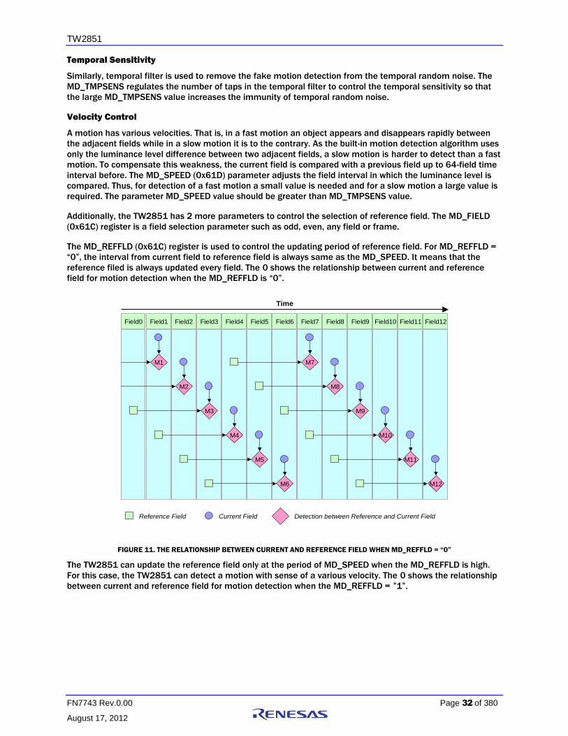
TW2851
FN7743 Rev.0.00 Page 32 of 380
August 17, 2012
Temporal Sensitivity
Similarly, temporal filter is used to remove the fake motion detection from the temporal random noise. The
MD_TMPSENS regulates the number of taps in the temporal filter to control the temporal sensitivity so that
the large MD_TMPSENS value increases the immunity of temporal random noise.
Velocity Control
A motion has various velocities. That is, in a fast motion an object appears and disappears rapidly between
the adjacent fields while in a slow motion it is to the contrary. As the built-in motion detection algorithm uses
only the luminance level difference between two adjacent fields, a slow motion is harder to detect than a fast
motion. To compensate this weakness, the current field is compared with a previous field up to 64-field time
interval before. The MD_SPEED (0x61D) parameter adjusts the field interval in which the luminance level is
compared. Thus, for detection of a fast motion a small value is needed and for a slow motion a large value is
required. The parameter MD_SPEED value should be greater than MD_TMPSENS value.
Additionally, the TW2851 has 2 more parameters to control the selection of reference field. The MD_FIELD
(0x61C) register is a field selection parameter such as odd, even, any field or frame.
The MD_REFFLD (0x61C) register is used to control the updating period of reference field. For MD_REFFLD =
“0”, the interval from current field to reference field is always same as the MD_SPEED. It means that the
reference filed is always updated every field. The 0 shows the relationship between current and reference
field for motion detection when the MD_REFFLD is “0”.
Field0
M1
Field1 Field2 Field3
M2
M3
M4
M5
M6
Field4 Field5 Field6 Field7 Field8 Field9 Field10 Field11 Field12
M7
M8
M9
M10
M11
M12
Time
Reference Field Detection between Reference and Current FieldCurrent Field
FIGURE 11. THE RELATIONSHIP BETWEEN CURRENT AND REFERENCE FIELD WHEN MD_REFFLD = “0”
The TW2851 can update the reference field only at the period of MD_SPEED when the MD_REFFLD is high.
For this case, the TW2851 can detect a motion with sense of a various velocity. The 0 shows the relationship
between current and reference field for motion detection when the MD_REFFLD = ”1”.

TW2851
FN7743 Rev.0.00 Page 33 of 380
August 17, 2012
Field0
M1
Field1 Field2 Field3
M2
M3
M4
M5
M6
Field4 Field5 Field6 Field7 Field8 Field9 Field10 Field11 Field12
M7
M8
M9
M10
M11
M12
Time
Reference Field Detection between Reference and Current FieldCurrent Field
FIGURE 12. THE RELATIONSHIP BETWEEN CURRENT AND REFERENCE FIELD WHEN MD_REFFLD = “1”
The TW2851 also supports the manual detection timing control of the reference field/frame via the
MD_STRB_EN and MD_STRB (0x61A) register. For MD_STRB_EN = “0”, the reference field/frame is
automatically updated and reserved on every reference field/frame. For MD_STRB_EN = “1”, the reference
field/frame is updated and reserved only when MD_STRB = “1”. In this mode, the interval between current
and reference field/frame depends on user’s strobe timing. This mode is very useful for a specific purpose
like non-periodical velocity control and very slow motion detection.
The TW2851 also provides dual detection mode for non-real-time application such as pseudo-8ch application
via MD_DUAL_EN (0x61A) register. For MD_DUAL_EN = 1, the TW2851 can detect dual motion independently
for VIN_A and B Input which is defined by the ANA_SWn (n=0~3) at 0x057 register. In this case, the
MD_SPEED is limited to 31.
BLIND DETECTION
The TW2851 supports a blind detection for each of the 4 analog video inputs and generated an interrupt to
the host when a blind condition is detected. A blind condition is detected when a camera is shaded / blocked
by some unknown object and the video level in wide area of a field is almost equal to average video level of
the field.
The TW2851 has two sensitivity parameters to detect blind input such as the level sensitivity via the
BD_LVSENS (0x61E) register and spatial sensitivity via the BD_CELSENS (0x61A) register.
The TW2851 uses total 768 (30x224) cells in full screen for blind detection. The BD_LVSENS parameter
controls the threshold of level between cell and field average. The BD_CELSENS parameter defines the
number of cells to detect blind. For BD_CELSENS = “0”, the number of cell whose level is same as average of
field should be over than 60% to detect blind, 70% for BD_CELSENS = “1”, 80% for BD_CELSENS = “2”, and
90% for BD_CELSENS = “3”. That is, the large value of BD_LVSENS and BD_CELSENS makes blind detector
less sensitive.
The TW2851 also supports dual detection mode for non-real-time application such as pseudo-8ch application
via the MD_DUAL_EN (0x61A) register. The host can read blind detection information for both VIN_A and
VIN_B input via MCU interrupt. When blind input is detected in any video inputs, the host processor can read
the information by accessing the INTERRUPT_VECT2 (0x1D2) register. This status information is updated in
the vertical blank period of each input.

TW2851
FN7743 Rev.0.00 Page 34 of 380
August 17, 2012
NIGHT DETECTION
The TW2851 supports night detection for each of the 4 analog video inputs and generates an interrupt to the
host when a night condition is detected. If an average of a field video level is very low, this input is interpreted
as night. Otherwise, the input is treated as day.
The TW2851 has two sensitivity parameters to detect night input such as the level sensitivity via the
ND_LVSENS (0x61F) register and the temporal sensitivity via the ND_TMPSENS (0x61F) register. The
ND_LVSENS parameter controls threshold level of day and night. The ND_TMPSENS parameter regulates the
number of taps in the temporal low pass filter to control the temporal sensitivity. The large value of
ND_LVSENS and ND_TMPSENS makes night detector less sensitive.
The TW2851 also supports dual detection mode for non-real-time application such as pseudo-8ch application
via the MD_DUAL_EN (0x61A) register. The host can read night detection information for both VIN_A and
VIN_B input via the MCU interrupt. When night input is detected in any video inputs, the TW2851 provides the
interrupt request to host via the IRQ pin. The host processor can read the information of night detection by
accessing the INTERRUPT_VECT1 (0x1D1) register. This status information is updated in the vertical blank
period of each input.
Digital Video Input
The TW2851 supports digital video input in 8-bit ITU-R BT.656, 16-bit BT.601, and 16-bit BT.1120 standards.
It has built-in ITU-R BT 656/601/1120 decoders. The digital video input can be used to display single-channel
video from any source, or to display a multi-channel video stream generated from a decompression engine.
In the multi-channel stream case, there will be channel ID information embedded in the video stream to
allow the downstream modules to de-multiplex the video stream. When using the digital video input in
BT.1120 format, TW2851 only supports single channel video.
ITU-R BT. 656 DIGITAL VIDEO INPUT FORMAT
When receiving video input in the BT. 656 format, TW2851 is capable of running at up to 4X clock rate of
108 MHz. With this a multi-channel field interleaved video stream of 8 half D1 field rate can be received
through a single 8-bit digital interface. TW2851 is able to de-multiplex the single video stream, extracts 4
channels, and perform cropping/scaling function on each channel independently. The timing of BT. 656
digital video input is illustrated in Figure 13.

TW2851
FN7743 Rev.0.00 Page 35 of 380
August 17, 2012
PBCLK
PBIN[7:0] Cb0 Y0 Cr080h 10h 80h 10h FFh 00h 00h00h 00h XYFFh XY Y1
EAV code SAV code
Cb2 Y2 Cr2 Y3 Cb4 Y4 Cr4 Y5 Cb6 Y6 Cr6 Y7 Cb8 Y8 Cr8 Y9
Horizontal Blanking Period Horizontal Active Period
FIGURE 13. TIMING DIAGRAM OF ITU-R BT. 656 FORMAT
TW2851 has a built-in BT. 656 decoder with error correction for decoding SAV/EAV information. The SAV and
EAV sequences are shown in Table 2.
TABLE 2. ITU-R BT.656 SAV AND EAV CODE SEQUENCE
CONDITION 656 FVH VALUE SAV/EAV CODE SEQUENCE
FIELD VERTICAL HORIZONTAL F V H FIRST SECOND THIRD FOURTH
EVEN Blank EAV
1 1 1
0xFF 0x00 0x00
0xF1
SAV 0 0xEC
EVEN Active EAV
1 0 1 0xDA
SAV 0 0xC7
ODD Blank EAV
0 1 1 0xB6
SAV 0 0xAB
ODD Active EAV
0 0 1 0x9D
SAV 0 0x80

TW2851
FN7743 Rev.0.00 Page 36 of 380
August 17, 2012
ITU-R BT. 601 DIGITAL VIDEO INPUT FORMAT
The digital video input can also take 16-bit ITU-R BT.601 standard. Additional signals such as HSYNC and
VSYNC are used for video timing control. The BT. 601 interface is able to run up to 4X clock rate (54 MHz) as
well. With this a multi-channel field/frame interleaved video stream of 4 D1 frame rate can be received
through a single 16-bit digital interface. Again, the TW2851 is able to de-multiplex this single video stream
into 4 channels, and perform cropping/scaling function on each channel independently.
The timing of BT. 601 digital video input is illustrated in
Front Porch Vertical Active Area Back Porch Front Porch Back PorchVertical Active Area
Top Field Bottom Field
VSYNC
HSYNC
DATA[15:0]
FIGURE 14. THE VSYNC/HSYNC TIMING IN BT. 601 INTERFACE
Note that there is no field ID input. The field information is derived from the leading edge of the VSYNC
signal. If this leading edge falls into a window (say, +/- N clock cycles) around the leading edge of HSYNC
signal, then the following field is top field. If it does not fall into such window, then the following field is
bottom field. The leading edge of the the VSYNC signal is the timing the field signal toggles.
ITU-R BT. 1120 DIGITAL VIDEO INPUT FORMAT
The digital video input can also take video streams in 16-bit ITU-R BT.1120 format. The BT. 1120 format
supports 1920x1125 (60 Hz) or 1920x1250 (50 Hz) resolution with a clock rate up to 74.25 MHz. The
BT.1120 input channel is a single channel video interface. There is no multi-channel interleaving or channel
ID support. Similar to the BT. 656 stream, the timing control signals are embedded in the data stream
through EAV/SAV header, defined the same way as BT. 656 in Table 2.
MULTI-CHANNEL VIDEO FORMAT
The video stream generated by TW2851 carries multi-channel video stream, which consists of multiple video
channels interleaved in one video stream. The multiple channels can be time interleaved in unit of a field (or
a frame when running at 27 MHz), or space multiplexed (in unit of CIF picture). The time/space multiplexed
format can vary flexibly from field/frame to field/frame. The “Picture Type” specifies how the multiple
channels are put together in each field/frame. There are total of 8 possible ways, as listed in the following
figure. Note that there are 4 channels at most in each field. The auto-channel ID in the VBI carries up to 4
channel IDs as well. The first channel ID will be CH_0. The second, third and forth being CH_1, CH_2, and
CH_3 correspondingly. Figure 15 shows how the 4 channel IDs are mapped into each field. Note that the
“Picture Type” automatically defines the picture size of each channel. The Auto-Channel ID in the VBI
specifies the location of each channel. When there are 4 channels, the size of each channel is evenly divided
from the full size of the picture. These various picture types are provided to allow external CODEC to make
use the stream as easy as possible. The CODEC can pick whatever is most fit into the design of their chip. Out
of the many types planned, the current TW2851 revB2 only supports field interleaving (type 0/2/) at
108/54/27 MHz, and frame interleaving (type 1 / 3) at 27 MHz.
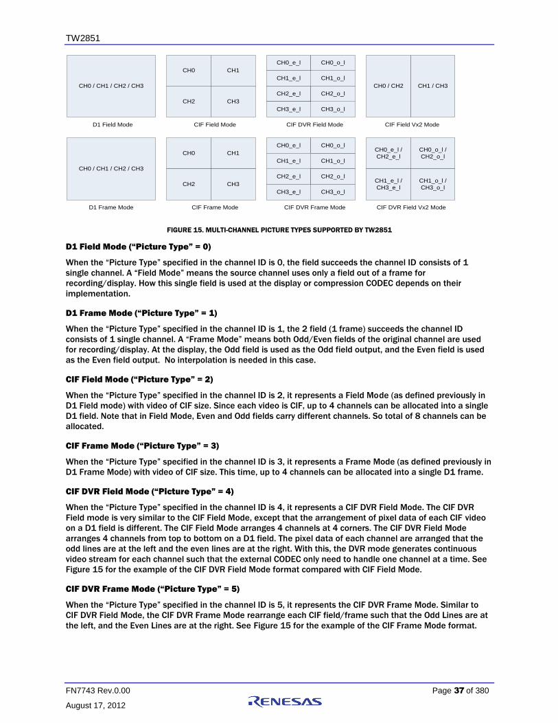
TW2851
FN7743 Rev.0.00 Page 37 of 380
August 17, 2012
CH0 CH1
CH2 CH3
CH0 / CH1 / CH2 / CH3 CH1 / CH3CH0 / CH2
CH0_e_l /
CH2_e_l
CH1_e_l /
CH3_e_l
CH0_o_l /
CH2_o_l
CH1_o_l /
CH3_o_l
CIF DVR Field Vx2 Mode
CIF Field Vx2 ModeCIF Field ModeD1 Field Mode
CH0_e_l
CH1_o_l
CH2_e_l
CH3_o_l
CIF DVR Field Mode
CH0_o_l
CH1_e_l
CH2_o_l
CH3_e_l
CH0 / CH1 / CH2 / CH3
D1 Frame Mode
CH0 CH1
CH2 CH3
CIF Frame Mode
CH0_e_l
CH1_o_l
CH2_e_l
CH3_o_l
CIF DVR Frame Mode
CH0_o_l
CH1_e_l
CH2_o_l
CH3_e_l
FIGURE 15. MULTI-CHANNEL PICTURE TYPES SUPPORTED BY TW2851
D1 Field Mode (“Picture Type” = 0)
When the “Picture Type” specified in the channel ID is 0, the field succeeds the channel ID consists of 1
single channel. A “Field Mode” means the source channel uses only a field out of a frame for
recording/display. How this single field is used at the display or compression CODEC depends on their
implementation.
D1 Frame Mode (“Picture Type” = 1)
When the “Picture Type” specified in the channel ID is 1, the 2 field (1 frame) succeeds the channel ID
consists of 1 single channel. A “Frame Mode” means both Odd/Even fields of the original channel are used
for recording/display. At the display, the Odd field is used as the Odd field output, and the Even field is used
as the Even field output. No interpolation is needed in this case.
CIF Field Mode (“Picture Type” = 2)
When the “Picture Type” specified in the channel ID is 2, it represents a Field Mode (as defined previously in
D1 Field mode) with video of CIF size. Since each video is CIF, up to 4 channels can be allocated into a single
D1 field. Note that in Field Mode, Even and Odd fields carry different channels. So total of 8 channels can be
allocated.
CIF Frame Mode (“Picture Type” = 3)
When the “Picture Type” specified in the channel ID is 3, it represents a Frame Mode (as defined previously in
D1 Frame Mode) with video of CIF size. This time, up to 4 channels can be allocated into a single D1 frame.
CIF DVR Field Mode (“Picture Type” = 4)
When the “Picture Type” specified in the channel ID is 4, it represents a CIF DVR Field Mode. The CIF DVR
Field mode is very similar to the CIF Field Mode, except that the arrangement of pixel data of each CIF video
on a D1 field is different. The CIF Field Mode arranges 4 channels at 4 corners. The CIF DVR Field Mode
arranges 4 channels from top to bottom on a D1 field. The pixel data of each channel are arranged that the
odd lines are at the left and the even lines are at the right. With this, the DVR mode generates continuous
video stream for each channel such that the external CODEC only need to handle one channel at a time. See
Figure 15 for the example of the CIF DVR Field Mode format compared with CIF Field Mode.
CIF DVR Frame Mode (“Picture Type” = 5)
When the “Picture Type” specified in the channel ID is 5, it represents the CIF DVR Frame Mode. Similar to
CIF DVR Field Mode, the CIF DVR Frame Mode rearrange each CIF field/frame such that the Odd Lines are at
the left, and the Even Lines are at the right. See Figure 15 for the example of the CIF Frame Mode format.

TW2851
FN7743 Rev.0.00 Page 38 of 380
August 17, 2012
CIF Vx2 Field Mode (“Picture Type” = 6)
When the “Picture Type” specified in the channel ID is 6, it represents a CIF Vx2 Field Mode. The Vx2 mode
means captures 2X of vertical lines of the field size to be display. With 2X of lines, the Odd lines are used for
Odd field, and the Even lines are used for Even field. This mode is intended to capture a single field while
used as a Frame at the output without interpolation. See Figure 15 for the CIF Vx2 Field Mode format.
CIF Vx2 DVR Field Mode (“Picture Type” = 7)
When the “Picture Type” specified in the channel ID is 7, it represents a CIF Vx2 DVR Field Mode. This mode is
a combination of Vx2, DVR, and Field Mode. See Figure 15 for the CIF Vx2 Field Mode format.
4D1 Frame Mode (“Picture Type” = 9)
Picture Type 9 is very similar to Picture Type 3, except the frame size is 4 times bigger. The Picture Type 3
uses a D1 frame to carry 4 CIF channels, while the Picture Type 9 uses a BT 1120 frame to carry 4 D1
channels. To use this type, the input PB port is configured as BT. 1120 port, and the VACTIVE / HACTIVE size
are configured to 4D1 rather than 1D1.
PLAYBACK INPUT CHANNEL DE-MULTIPLEXER
TW2851 supports up to four playback digital input ports (PB0 ~ PB3), each carries multiple channels within
the video stream. The PB0 ~ PB3 can be in either of 8-bit, 16-bit or 24-bit playback interfaces in BT. 656, BT.
601, BT. 1120, or component RGB format. There are total of 32 PB data input pins which can be flexibly
configured in various input configurations, as shown in Table 3.
TABLE 3. PLAYBACK INPUT CONFIGURATIONS
PB0_TYPE PB1_TYPE PB PORT 0 PB PORT 1 PB PORT 2 PB PORT 3
0
0 PB0_DIN[7:0]
BT. 656
PB1_DIN[15:8]
BT. 656
PB2_DIN[23:16]
BT. 656
PB3_DIN[31:24]
BT. 656
1
1
0 U / V = PB0_DIN[7:0]
Y = PB1_DIN[7:0]
BT. 601
PB2_DIN[23:16]
BT. 656
PB3_DIN[31:24]
BT. 656
1
U / V = PB2_DIN[7:0]
Y = PB3_DIN[7:0]
BT. 601
2
0
U / V = PB0_DIN[7:0]
Y = PB1_DIN[7:0]
BT. 1120
PB2_DIN[23:16]
BT. 656
PB3_DIN[31:24]
BT. 656
1
U / V = PB2_DIN[7:0]
Y = PB3_DIN[7:0]
BT. 601
3 X
R / V = PB2_DIN[7:0]
G / Y = PB1_DIN[7:0]
B / U = PB0_DIN[7:0]
PB3_DIN[31:24]
BT. 656

TW2851
FN7743 Rev.0.00 Page 39 of 380
August 17, 2012
The playback interface matches the desired channel number set in PB_CHNUM (0x160, 0x170, 0x180,
0x190) with the channel IDs embedded within the video stream from each of the 4 ports, and generates up
to 4 matched single-channel video streams (PB_CH0 ~ PB_CH3). Each of the PB_CH0 ~ PB_CH3 are single
channel that can be cropped / scaled individually before writing into the DDR memory. The matching process
generates the control signals PB_PORT_SEL0 ~ PB_PORT_SEL3 to select one of the 4 physical ports PB0 ~
PB3 for each of the PB_CH0 ~ PB_CH3 channel. The automatic matching result PB_PORT_SEL0 ~
PB_PORT_SEL3 can be read from register 0x101. Figure 16 shows how the input video streams from PB0 ~
PB3 are each checked against the PB_CHNUM, and de-multiplexed into 4 single channels PB_CH0 ~ PB_CH3.
PB0 CHID
Matching
CHID
Decoding
PB1 CHID
Matching
CHID
Decoding
PB2 CHID
Matching
Manual
CHID
Setting
PB3 CHID
Matching
Manual
CHID
Setting
PB_CH0
PB_CH1
PB_CH2
PB_CH3
PB_PORT_SEL0*
PB_PORT_SEL1*
PB_PORT_SEL2*
PB_PORT_SEL3*
FIGURE 16. PLAYBACK INPUT DE-MULTIPLEXER

TW2851
FN7743 Rev.0.00 Page 40 of 380
August 17, 2012
CHANNEL ID DECODER
In a multi-channel video stream, the channel ID information associated with each field / frame is embedded
in the video vertical blanking area right before the active field in order to identify the channels of pictures in
that active field. A channel ID decoder extracts and provides this information, including “channel IDs”,
“Picture Type”, to the crop / scale module to separate the multi-channel video stream into multiple single-
channel video streams. In addition, an auto strobe signal is generated if the decoded channel ID matches the
PB_CHNUM in 0x160, 0x170, 0x180, and 0x190. This signal is sent along with the separated single-channel
video streams to the write control module to capture the picture automatically into the external video buffer.
The first two digital input ports (PB0, PB1) are equipped with a channel ID decoder and channel ID matching
module to match and de-multiplex the multiple video streams automatically. In addition, a manual channel
ID setting can be used to replace the result from channel ID decoder. All 4 PB ports have the manual channel
ID setting through the registers in 0x120 ~ 0x123, 0x130 ~ 0x133, 0x140 ~ 0x143, and 0x150 ~ 0x153. The
manual channel ID setting is enabled by setting PBm_MAN_STRB_EN (0x120 / 0x130 / 0x140 / 0x150) to
“1”. The manual channel ID is useful if the incoming video stream does not carry any channel ID information
in its VBI. Note, however, that when the manual channel IDs are used, it cannot vary from field to field. Those
picture types with channel ID changing from field to field cannot be supported.
With 4 playback input ports, there are a maximum of 16 channels embedded in the incoming streams. The
playback path is designed to extract 4 out of the 16 channels. There are 4 sets of channel ID registers
PB_CHNUM0 ~ PB_CHNUM3 (0x160, 0x170, 0x180, 0x190) used for the matching module of each port. Each
port will generate up to 4 channels. The PB_CHNUM is a 5 bit ID, including the 2-bit chip ID (in cascade case),
2-bit port ID, and 1-bit of analog ID that needs to be matched with the PB_ANAx (0x160, 0x170, 0x180,
0x190) to support Pseudo 8 channel application. If there are same Channel IDs extracted from more than 1
port, only the channel from the lowest playback port number is used. For details of Channel ID information
embedded in VBI, please refer to the section on page 56.
CROPPING AND SCALING FUNCTION
The TW2851 supports the cropping and scaling function at the output of channel de-multiplexer behind the
digital input port. There are 4 cropping / scaling modules which use the decoded channel ID to automatically
crop the multi-channel stream into multiple single-channel streams and match the input Picture Type / size
automatically.
Cropping
Similar to the cropping function in the analog CVBS path, the digital video input interface provides a cropping
function to crop video into a smaller size as required by application. The active video region is determined by
the HDELAY, HACTIVE, VDELAY and VACTIVE registers (0x124 ~ 0x129, 0x134 ~ 0x139, 0x144 ~ 0x149,
0x154 ~ 0x159). The first active line is defined by the VDELAY register and the first active pixel is defined by
the HDELAY register. The VACTIVE register can be programmed to define the number of active lines in a video
field, and the HACTIVE register can be programmed to define the number of active pixels in a video line.
The cropping feature is also used for input video streams with multiple channel of video on the same field
(e.g. PIC_TYPE 2 or 3) to separate out the intended channel from others. In this case, however, the HDELAY,
VDELAY, HACTIVE, VACTIVE settings refer to the whole size of the field, instead of the size of each channel.
The cropping function will automatically do additional cropping based on the PIC_TYPE information to
separate out the single channel.

TW2851
FN7743 Rev.0.00 Page 41 of 380
August 17, 2012
Scaling
The scaling function in digital input path is similar to the downscalers in the video decoder path. A setting of
source and target video size are specified through register 0x162 ~ 0x165, 0x172 ~ 0x175, 0x182 ~ 0x185,
and 0x192 ~ 0x195. The scalers used here are downscalers that can down scale freely to any size in multiple
of 16-pixel steps. In case of CIF input that needs to be upscaled to D1, the TW2851 also provides a simple
upscaler that can upscale the input at a fixed 2X scaling factor. This is set through PB_H2X_EN in registers
0x161, 0x171, 0x181, 0x191, and DP_RD_V_2Xn (n= 0 ~ 3) in registers 0x250, 0x258, 0x260, and 0x268.
The use of downscaler and upscaler can be turned on simultaneously to achieve scaling factor up to 2X the
original size horizontally and vertically.
Video Multiplexers
The TW2851 has three sets of video multiplexers, one for display, SPOT and record path each. All three
multiplexers utilize a centralized external 256 Mbits DDR DRAM through a 16-bit data bus interface. The
control of multiplexers are through the way the video are captured and read back to / from the external DDR
SDRAM. The TW2851 supports 8-channel inputs for display path, 4-channel for SPOT path, and 4-channel for
record path. The block diagram of video controller is shown in Figure 17.
To
OSD
Overlay
Control
Part
Write
Control
Memory Interface
256M DDR DRAM @ 16 Bit Data
Zoom&
ImageEnhance
VGA_X
VOUT_Y0
PB0_X
PB1_X
PB2_X
PB3_X
From
Video
Input
PartRead
Control
VIN0_X
VIN1_X
VIN2_X
VIN3_X
VIN0_Y
VIN1_Y
VIN2_Y
VIN3_Y
8X8
INPUT
MUX
VIN0_S
VIN1_S
VIN2_S
VIN3_SVOUT_SScaling &
Overlay
CHID
Encoding VOUT_Y1
DNSCVBS_X
FIGURE 17. BLOCK DIAGRAM OF VIDEO CONTROLLER
CAPTURE CONTROL
Each of the Display / Record / SPOT paths supports video capturing in two different ways: LIVE mode and
STROBE mode. In LIVE mode, every incoming video is updated into the video buffer to show up at the output.
In STROBE mode, the incoming video is updated only if a strobe signal is issued either internally on the chip
or externally from the MCU.
There are two different strobe modes supported. One is the AUTO STROBE mode, one is the MANUAL STROBE
mode. The video streams from the playback interface can run at the AUTO STROBE mode, where a strobe
signal is generated on chip automatically through channel ID decoding and matching circuit. The video
streams from the video decoder only runs at MANUAL STROBE mode. Each channel can be independently

TW2851
FN7743 Rev.0.00 Page 42 of 380
August 17, 2012
operated in its own mode, either LIVE or STROBE mode. Table 4 shows the modes supported on each of the
display / SPOT / record path.
TABLE 4. CAPTURE MODES SUPPORT OF DISPLAY/SPOT/RECORD PATHS
LIVE MODE STROBE MODE
DISPLAY / VD YES MANUAL
DISPLAY / PB YES AUTO
SPOT YES MANUAL
RECORD YES MANUAL
Display Capture Modes
The display path capture mode is controlled by the DP_FUNC_MD (0x250 ~ 0x288).
Live Mode (DP_FUNC_MD = 0)
The LIVE mode captures every incoming field / frame into the video buffer into the external DDR memory. For
inputs from video decoder, the input is always frame based. Every frame is updated and shown as a real-time
video stream. For inputs from playback input, the capture mode is usually Auto Strobe Mode. However,
playback LIVE mode can be forced on if PB_FORCE_LIVE (0x123, 0x133, 0x143, 0x153) is set to ‘1’. Under
this mode, the incoming video stream always shows up independently of the PB_CHNUM setting. The
PB_FORCE_LIVE = 1 only take D1 frame mode. So the PBn_MAN_PIC_TYPE has to be set to 0x01 in this type.
The LIVE mode capturing can be over-ruled with a freeze control by setting DP_FREEZEm register
(0x250/0x258/0x260/0x268/0x270/0x278/0x280/0x288) to 1. In this case, the incoming video will no
longer been captured until this bit is cleared.
Auto Strobe Mode (DP_FUNC_MD = 0)
For playback digital inputs, a strobe can be provided automatically if there is a matching of PB_CHNUM with
the channel ID from VBI or from the manual mode setting. The TW2851 provides a channel ID matching
mechanism to strobe only at the valid field / frame that matches the channel ID. The auto strobe mode
capturing can also be over-ruled by a freeze control by setting DP_FREEZEm register
(0x250/0x258/0x260/0x268/0x270/0x278/0x280/0x288) to 1. In this case, the incoming video will no
longer been captured even though there is a channel ID match, until this bit is cleared.
Manual Strobe Mode (DP_FUNC_MD = 1)
The strobe mode of display path is mainly used to support the pseudo 8 channel mode. When the video
decoder is switching between VINA and VINB, the MCU is responsible for the timing of switching the
multiplexer. After switching, the MCU wait for a certain amount of delay time until the video picture is stable,
then issue the DP_STRB_REQ (0x24F) signal. The display path then captures a field/frame depending on the
setting of DP_STRB_FLD (0x250 ~ 0x288). Once the capture is completed, the display module clears the
DP_STRB_REQ signal. The MCU poll the DP_STRB_REQ signal, and perform the switching all over again.
Record/SPOT Capture Modes
The record/SPOT path also supports either LIVE and STROBE mode individually for each port. The mode is
controlled by RP_FUNC_MD_n (0x210 ~ 0x213, 0x2A0 ~ 0x2A3). Each port can be configured to LIVE mode
or STROBE mode individually using the FUNC_MD.
Live Mode (RP_FUNC_MD_n = 0)
In LIVE mode, the capture module captures every received field/frame into the video buffer into the external
DDR memory. Depending on the RP_PIC_TYPE / SP_PIC_TYPE (0x215, 0x2A5), the captured field/frame is
updated either per frame or per field. In addition to the existing picture type defined, the SPOT path also
supports an additional picture type that allows all 16 channels QCIF to cascade onto one single output.

TW2851
FN7743 Rev.0.00 Page 43 of 380
August 17, 2012
Strobe Mode (RP_FUNC_MD_n = 1)
The strobe mode captures a field / frame each time a strobe request is issued by the MCU. This allows the
MCU to control the timing of capturing a field/frame, and is useful in supporting pseudo 8 channel. In
pseudo 8 channel mode, the MCU switches the analog multiplexer from VINA to VINB, waits for a certain
amount of time till the picture is stable, and issues a strobe signal to RP_STROBE_n / SP_STROBE_n (0x214,
0x2A4). Once a field/frame is captured, the strobe signal is cleared automatically. The MCU can poll this bit
for capture completion, and starts the switching process all over again.
READ CONTROL
The read control arranges the input channels at the output port in terms of both temporal control and spatial
control. The spatial control specifies the location and the channel of each enabled window at the output. The
temporal control specifies how the multiple channels are temporally interleaved to share the frame rate
efficiently. Therefore each field / frame can carry video from different channels. For display path, every
enabled window shows up all the time. No temporal control is involved. For record / SPOT path, the channels
can be field / frame interleaved.
The control of temporal / spatial configurations is through either static register, or dynamic switch queue. The
static control specifies the spatial / temporal control through a set of registers. The switch queue specifies
the spatial / temporal control through a switch queue, with each entry of the queue determine the control in
a field / frame.
Display Read Control
For display path, the output channel does not change from field to field. So there is no temporal control.
Spatially, the display path can show up to 8 video windows on the output monitor. In implementation, the
window 0 has highest priority, and window 7 has lowest priority. Window 0 always stays on top, and covers
other windows. Every video window is flexibly configurable in terms of size and location and is controlled by
DP_PICHLm (0x252, 0x25A, 0x262, 0x26A, 0x272, 0x27A, 0x282, 0x28A), DP_PICHRm (0x253, 0x25B,
0x263, 0x26B, 0x273, 0x27B, 0x283, 0x28B), DP_PICVTm (0x254, 0x25C, 0x264, 0x26C, 0x274, 0x27B,
0x284, 0x28B), and DP_PICVBm (0x255, 0x25D, 0x265, 0x26D, 0x275, 0x27D, 0x285, 0x28D) for the left,
right, top, bottom of each window.
The display path supports 8 input channels to fill into the 8 video windows. Channel 0 ~ 3 take inputs from
either playback channel 0 ~ 3, or video decoder port 0 ~ 3 with analog selection 0 or 1. Channel 4 ~ 7 take
inputs from video decoders 0 ~ 3 with analog selection 0 or 1. The Table 5 shows the input selections the
display channel can support. Note that DP_PBVD_SEL is 4 bits. It controls each of channel 0 ~ 3 separately.
TABLE 5. DISPLAY CHANNEL CONFIGURATION
DISPLAY
CHANNEL #
PLAYBACK WITH 4
VD CHANNELS
DP_PBVD_SEL = 0
PSEUDO 8
CHANNELS
DP_PBVD_SEL = 1
0 PB_CH0 VD_0 (A/B)
1 PB_CH1 VD_1 (A/B)
2 PB_CH2 VD_2 (A/B)
3 PB_CH3 VD_3 (A/B)
4 VD_0 (A/B) VD_0 (A/B)
5 VD_1 (A/B) VD_1 (A/B)
6 VD_2 (A/B) VD_2 (A/B)
7 VD_3 (A/B) VD_3 (A/B)
The display path display supports cascade function, allowing 4 chips of TW2851 to be connected together
and merge all the windows into one single VGA / CVBS output. With 4-chip cascade, the display output can
TW2851
FN7743 Rev.0.00 Page 44 of 380
August 17, 2012
support up to 32 windows in total. The priority of all video windows will be the downstream chips cover the
upstream chips.
Record/SPOT Static Control (RP_SM_EN / SP_SM_EN = 0)
To run the record / SPOT path at static mode, the RP_SM_EN / SP_SM_EN register (0x215, 0x2A5 for SPOT)
is set to “0”. Instead of arranging all windows flexibly as in the display path, the Record / SPOT path read
control is less flexible. It uses the pre-specified configuration, described as picture types, shown in Figure 15,
with each window either full screen or 1/4 of the whole screen. The windows cannot be overlapped in record
/ SPOT path.
The picture type of record / SPOT path in static mode is controlled by the RP_PIC_TYPE / SP_PIC_TYPE
(0x215, 0x295) register. For each of the picture type, the windows are arranged as follows.
PIC_TYPE of 0 / 1: The record / SPOT module output 1 field/frame from each of the channel
specified by CHNUM0 ~ CHNUM3 (0x21D, 0x21E for record, and 0x2AD, 0x2AE for SPOT). There is a
control CH_CYCLE (0x215 for record, 0x2A5 for SPOT) used to control how many ports are
interleaved. A CH_CYCLE setting of m allows m channels to be interleaved as specified in CHNUM0 ~
CHNUMm-1. The CHNUMm through CHNUM3 will be ignored. A CH_CYCLE “0” represents m=4.
PIC_TYPE of 2/3/4/5: The record captures 4 channels to form a 4-window screen with CHNUM0
represents the upper left window, CHNUM1 represents the upper right window, CHNUM2 represents
the lower left window, and CHNUM3 represents the lower right window. CH_CYCLE should be set to 1
for these types.
PIC_TYPE of 6/7: The record path captures 2 channels to from a 2-window screen, with CHNUM0/2
representing the left window, and the CHNUM1/3 representing the right window. The CH_CYCLE can
be set to 2 to interleave 4 channels into 2 fields.
An additional SPOT path 16-window QCIF mode allows all 16 ports of the 4 chip cascade configuration to be
shown on a single output with 16 QCIF window size on the SPOT output. In this case, the channels are static
from field to field, just like display path. To use this mode, the user set the SP_16 register (0x2C0) to 1, and
specify the location of the output windows with SP_16_WINNUM0 ~ SP_16_WINNUM3 (0x2C1, 0x2C2) for
each of the port 0 ~ 3.
Record/SPOT Switch Control (SM_EN = 1)
Switch Queue
The dynamic switch mode is designed to allow multiple channels to share the output frame rate through flexible way of frame/field interleaving of “Picture Type” described previously at the “Multi-channel Video Format” section. The “Picture Type” can be one of the 8 types in Figure 15 and can change from field / frame to field / frame. To achieve this, an internal Switch Queue (1024 entries in the record path and 16 entries in the SPOT path) is used to specify the “Picture Type”, “Channel IDs”, the Capturing Field (Odd or Even) of each field/frame. The input videos are multiplexed according to the Switch Queue to generate the output multi-channel video stream. The Switch Queue read pointer increments once per field for “Picture Type” of the Field Mode type, and increment once per frame when the “Picture Type” being one of the Frame Mode type. The definition of a switch queue entry is shown in Table 6 for record path and Table 7 for SPOT path.

TW2851
FN7743 Rev.0.00 Page 45 of 380
August 17, 2012
TABLE 6. SWITCH QUEUE ENTRY DEFINITION OF RECORD PATH
SWITCH QUEUE
ENTRY BIT RANGE FUNCTION
3 : 0 CHNUM0 (upper left window)
CHIP_ID + PORT_ID
7 : 4 CHNUM1 (upper right window)
CHIP_ID + PORT_ID
11 : 8 CHNUM2 (lower left window)
CHIP_ID + PORT_ID
15 : 12 CHNUM3 (lower right window)
CHIP_ID + PORT_ID
19 : 16 CHANNEL DISABLE
22 : 20 PICTURE_TYPE
23 STROBE_FIELD
27 : 24 Record OSG0 Control
31 : 28 Record OSG1 Control
TABLE 7. SWITCH QUENE ENTRY DEFINITION OF SPOT PATH
SWITCH QUEUE
ENTRY BIT RANGE FUNCTION
3 : 0 CHNUM0 (upper left window)
CHIP_ID + PORT_ID
7 : 4 CHNUM1 (upper right window)
CHIP_ID + PORT_ID
11 : 8 CHNUM2 (lower left window)
CHIP_ID + PORT_ID
15 : 12 CHNUM3 (lower right window)
CHIP_ID + PORT_ID
19 : 16 CHANNEL DISABLE
22 : 20 PICTURE_TYPE
23 STROBE_FIELD
With the switch queue defined, the output video can change configuration from field / frame to field / frame.
For example, the first field can be a whole screen channel (e.g. picture type 0), the second field can be a
quad-CIF screen (e.g. picture type 2), while the third/fourth fields being picture type 5. A switch queue size
register RP_SQ_SIZE / SP_SQ_SIZE (0x20E, 0x20F for record and 0x29E for SPOT) specifies the length of the
queue. The use of the switch queue will loop from the first entry to the SQ_SIZE entry and starts over again.
Switch Queue Configuration
To write an entry in the Switch Queue, the MCU configures the RP_SQ_ADDR (0x20D/0x20F) for record,
SP_SQ_ADDR (0x29D) for SPOT, RP_SQ_SIZE (0x20E/0x20F) for record, RP_SQ_SIZE (0x29F), set a “1” to
RP_SQ_WR (0x208) for record, SP_SQ_WR (0x298) for SPOT, Then write a queue entry data to RP_SQ_DATA
(0x209/0x20A/0x20B/0x20C) for record, SP_SQ_DATA (0x299/0x29A/0x29B) for SPOT. Once all these are
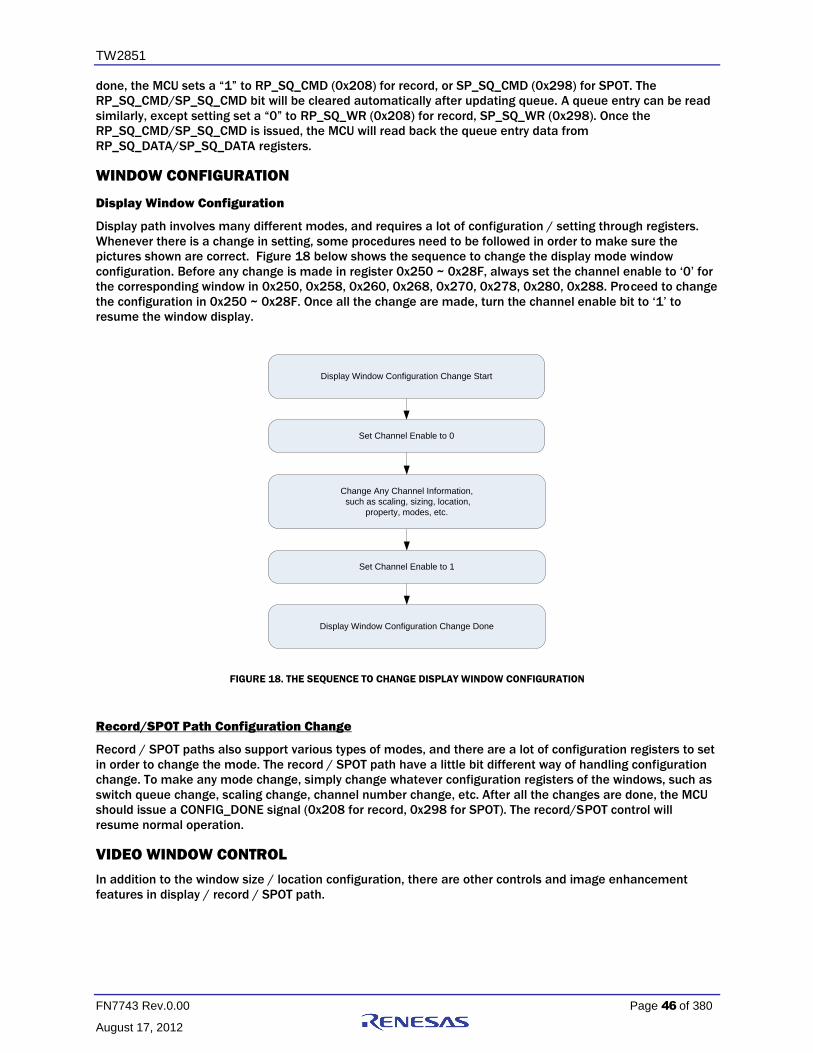
TW2851
FN7743 Rev.0.00 Page 46 of 380
August 17, 2012
done, the MCU sets a “1” to RP_SQ_CMD (0x208) for record, or SP_SQ_CMD (0x298) for SPOT. The
RP_SQ_CMD/SP_SQ_CMD bit will be cleared automatically after updating queue. A queue entry can be read
similarly, except setting set a “0” to RP_SQ_WR (0x208) for record, SP_SQ_WR (0x298). Once the
RP_SQ_CMD/SP_SQ_CMD is issued, the MCU will read back the queue entry data from
RP_SQ_DATA/SP_SQ_DATA registers.
WINDOW CONFIGURATION
Display Window Configuration
Display path involves many different modes, and requires a lot of configuration / setting through registers.
Whenever there is a change in setting, some procedures need to be followed in order to make sure the
pictures shown are correct. Figure 18 below shows the sequence to change the display mode window
configuration. Before any change is made in register 0x250 ~ 0x28F, always set the channel enable to ‘0’ for
the corresponding window in 0x250, 0x258, 0x260, 0x268, 0x270, 0x278, 0x280, 0x288. Proceed to change
the configuration in 0x250 ~ 0x28F. Once all the change are made, turn the channel enable bit to ‘1’ to
resume the window display.
Display Window Configuration Change Start
Display Window Configuration Change Done
Set Channel Enable to 1
Change Any Channel Information,
such as scaling, sizing, location,
property, modes, etc.
Set Channel Enable to 0
FIGURE 18. THE SEQUENCE TO CHANGE DISPLAY WINDOW CONFIGURATION
Record/SPOT Path Configuration Change
Record / SPOT paths also support various types of modes, and there are a lot of configuration registers to set
in order to change the mode. The record / SPOT path have a little bit different way of handling configuration
change. To make any mode change, simply change whatever configuration registers of the windows, such as
switch queue change, scaling change, channel number change, etc. After all the changes are done, the MCU
should issue a CONFIG_DONE signal (0x208 for record, 0x298 for SPOT). The record/SPOT control will
resume normal operation.
VIDEO WINDOW CONTROL
In addition to the window size / location configuration, there are other controls and image enhancement
features in display / record / SPOT path.
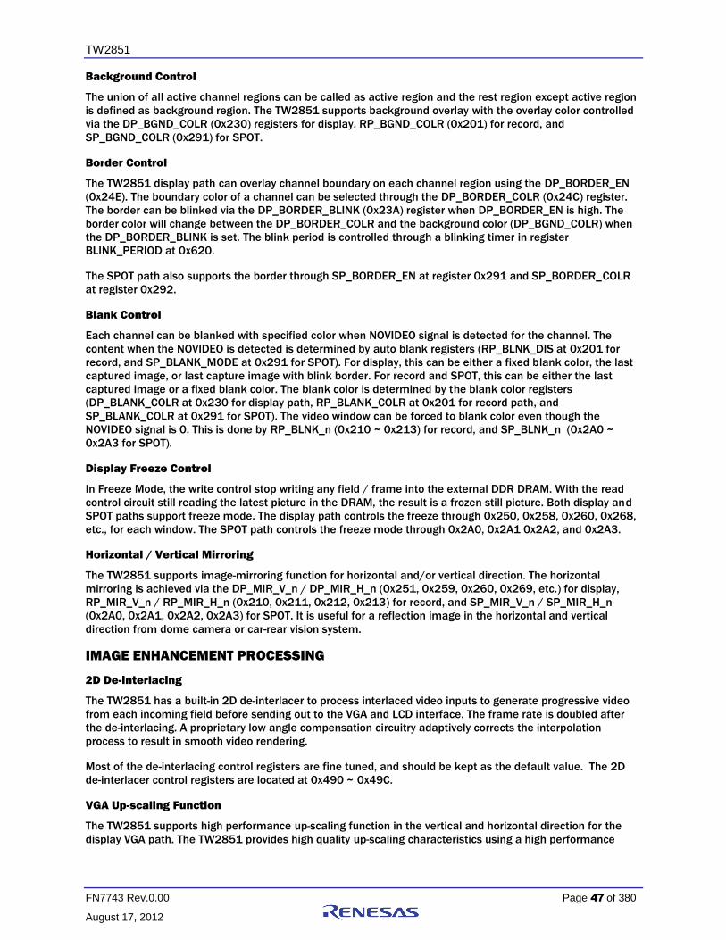
TW2851
FN7743 Rev.0.00 Page 47 of 380
August 17, 2012
Background Control
The union of all active channel regions can be called as active region and the rest region except active region
is defined as background region. The TW2851 supports background overlay with the overlay color controlled
via the DP_BGND_COLR (0x230) registers for display, RP_BGND_COLR (0x201) for record, and
SP_BGND_COLR (0x291) for SPOT.
Border Control
The TW2851 display path can overlay channel boundary on each channel region using the DP_BORDER_EN
(0x24E). The boundary color of a channel can be selected through the DP_BORDER_COLR (0x24C) register.
The border can be blinked via the DP_BORDER_BLINK (0x23A) register when DP_BORDER_EN is high. The
border color will change between the DP_BORDER_COLR and the background color (DP_BGND_COLR) when
the DP_BORDER_BLINK is set. The blink period is controlled through a blinking timer in register
BLINK_PERIOD at 0x620.
The SPOT path also supports the border through SP_BORDER_EN at register 0x291 and SP_BORDER_COLR
at register 0x292.
Blank Control
Each channel can be blanked with specified color when NOVIDEO signal is detected for the channel. The
content when the NOVIDEO is detected is determined by auto blank registers (RP_BLNK_DIS at 0x201 for
record, and SP_BLANK_MODE at 0x291 for SPOT). For display, this can be either a fixed blank color, the last
captured image, or last capture image with blink border. For record and SPOT, this can be either the last
captured image or a fixed blank color. The blank color is determined by the blank color registers
(DP_BLANK_COLR at 0x230 for display path, RP_BLANK_COLR at 0x201 for record path, and
SP_BLANK_COLR at 0x291 for SPOT). The video window can be forced to blank color even though the
NOVIDEO signal is 0. This is done by RP_BLNK_n (0x210 ~ 0x213) for record, and SP_BLNK_n (0x2A0 ~
0x2A3 for SPOT).
Display Freeze Control
In Freeze Mode, the write control stop writing any field / frame into the external DDR DRAM. With the read
control circuit still reading the latest picture in the DRAM, the result is a frozen still picture. Both display and
SPOT paths support freeze mode. The display path controls the freeze through 0x250, 0x258, 0x260, 0x268,
etc., for each window. The SPOT path controls the freeze mode through 0x2A0, 0x2A1 0x2A2, and 0x2A3.
Horizontal / Vertical Mirroring
The TW2851 supports image-mirroring function for horizontal and/or vertical direction. The horizontal
mirroring is achieved via the DP_MIR_V_n / DP_MIR_H_n (0x251, 0x259, 0x260, 0x269, etc.) for display,
RP_MIR_V_n / RP_MIR_H_n (0x210, 0x211, 0x212, 0x213) for record, and SP_MIR_V_n / SP_MIR_H_n
(0x2A0, 0x2A1, 0x2A2, 0x2A3) for SPOT. It is useful for a reflection image in the horizontal and vertical
direction from dome camera or car-rear vision system.
IMAGE ENHANCEMENT PROCESSING
2D De-interlacing
The TW2851 has a built-in 2D de-interlacer to process interlaced video inputs to generate progressive video
from each incoming field before sending out to the VGA and LCD interface. The frame rate is doubled after
the de-interlacing. A proprietary low angle compensation circuitry adaptively corrects the interpolation
process to result in smooth video rendering.
Most of the de-interlacing control registers are fine tuned, and should be kept as the default value. The 2D
de-interlacer control registers are located at 0x490 ~ 0x49C.
VGA Up-scaling Function
The TW2851 supports high performance up-scaling function in the vertical and horizontal direction for the
display VGA path. The TW2851 provides high quality up-scaling characteristics using a high performance
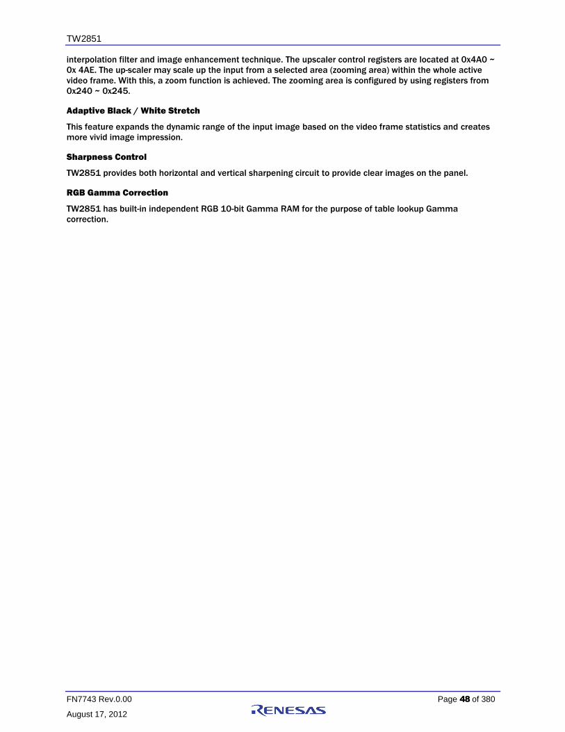
TW2851
FN7743 Rev.0.00 Page 48 of 380
August 17, 2012
interpolation filter and image enhancement technique. The upscaler control registers are located at 0x4A0 ~
0x 4AE. The up-scaler may scale up the input from a selected area (zooming area) within the whole active
video frame. With this, a zoom function is achieved. The zooming area is configured by using registers from
0x240 ~ 0x245.
Adaptive Black / White Stretch
This feature expands the dynamic range of the input image based on the video frame statistics and creates
more vivid image impression.
Sharpness Control
TW2851 provides both horizontal and vertical sharpening circuit to provide clear images on the panel.
RGB Gamma Correction
TW2851 has built-in independent RGB 10-bit Gamma RAM for the purpose of table lookup Gamma
correction.

TW2851
FN7743 Rev.0.00 Page 49 of 380
August 17, 2012
Video Output
TW2851 supports both analog and digital video outputs. Analog outputs include: display VGA output, two
CVBS output shared by display, record, and spot path. The digital outputs include: display RGB output, display
cascade output, display BT1120 output, record output 1 and 2 in 656 format, and SPOT output in 656
format.
Video
EncoderADC
Video
EncoderADC
ADC
ADC
ADC R
G
B
CVBS1
CVBS2
VGA
CNTLR
DISPLAY VGA
DISPLAY 656
DISPLAY CASCADE
LVDS/VDOX[15:8] RGB
or VDOX[15:0] YUV
RECORD_0 656
SPOT 656
VDOS[7:0]
RECORD_1 656
VDOY0[7:0]
VDOY1[7:0]
FIGURE 19. THE VIDEO OUTPUT BLOCK DIAGRAM
ANALOG VGA/RGB VIDEO OUTPUT
The TW2851 incorporate 3 higher performance DACs to provide analog RGB component output for display
VGA interface. In addition to the RGB component, the VGA VS / HS signal is also generated. The VGA output
supports various resolutions from VGA (640x480), SVGA (800x600), XGA (1024x768), SXGA (1280x1024),
and WXGA (1440x900). The VGA output video went through an on-chip 2D de-interlacer module to convert
the interlaced video signal into progressive and an up-scaler function to scale the internal 4D1 resolution
video into a screen size larger than 4D1.
CVBS VIDEO OUTPUT
The TW2851 supports analog video output using two built-in video encoders, which generates composite
video with a 10 bit DAC. The sources of the video encoder inputs are flexibly selectable from display and
SPOT path by setting VE_SEL (0x2D7, 0x2D8). Whatever the incoming video sources are, they have to be
running at 27 MHz in order to use the video encoder for CVBS output. The incoming digital video are adjusted
for gain and offset according to NTSC or PAL standard. Both the luminance and chrominance are band-
limited and interpolated to 27MHz sampling rate for digital to analog conversion. The NTSC output can be
selected to include a 7.5 IRE pedestal. The TW2851 also provides internal test color bar generation.
Output Standard Selection
The TW2851 on-chip video encoders support various video standard outputs via the VE_PAL_NTSC and
VE_FSCSEL (0x2D0), VE_PHALT, VE_PED (0x2D1) registers as described in the following Table 8.

TW2851
FN7743 Rev.0.00 Page 50 of 380
August 17, 2012
TABLE 8. ANALOG OUTPUT VIDEO STANDARDS
FORMAT
SPECIFICATION REGISTER
LINE/FV
(HZ) FH (KHZ) FSC (MHZ) PAL_NTSC ENC_ FSC ENC_PHALT ENC_PED
NTSC-M 525/59.94 15.734 3.579545 0 0 0
1
NTSC-J 0
NTSC-4.43 525/59.94 15.734 4.43361875 0 1 0 1
NTSC-N 625/50 15.625 3.579545 1 0 0 0
PAL-BDGHI 625/50 15.625 4.43361875 1 1 1
0
PAL-N 1
PAL-M 525/59.94 15.734 3.57561149 0 2 1 0
PAL-NC 625/50 15.625 3.58205625 1 3 1 0
PAL-60 525/59.94 15.734 4.43361875 0 1 1 0
If the VE_FDRST (0x2D1) register is set to “1”, phase alternation can be reset every 8 field so that phase
alternation keeps same phase every 8 field. The polarity of horizontal, vertical sync and field flag can be
controlled by the VE_HSPOL, VE_VSPOL and VE_FLDPOL (0x2D1) registers respectively. The TW2851 can
detect field polarity from vertical sync and horizontal sync via the VE_FLD (0x2D0) register or can detect
vertical sync from the field flag via the VE_VS (0x2D0) register. The detailed timing diagram is illustrated in
Figure 20.
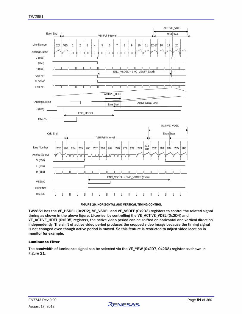
TW2851
FN7743 Rev.0.00 Page 51 of 380
August 17, 2012
ACTIVE_VDEL
Analog Output
Line Number
HSENC
VSENC
FLDENC
Analog Output
Line Number
HSENC
VSENC
FLDENC
VBI Full Interval
VBI Full Interval
524 525 1 2 3 4 5 6 7 8 9 10 11 12-17 18 19 20
Odd StartEven End
Even StartOdd End
262 263 264 265 266 267 268 269 270 271 272 273274-
281 282 283 284 285 286
ENC_VSDEL + ENC_VSOFF (Odd)
ENC_VSDEL + ENC_VSOFF (Even)
H (656)
V (656)
F (656)
H (656)
F (656)
V (656)
HSENC
ENC_HSDEL
Analog Output
ACTIVE_HDEL
ACTIVE_VDEL
H (656)
Active Data / LineLine Start
FIGURE 20. HORIZONTAL AND VERTICAL TIMING CONTROL
TW2851 has the VE_HSDEL (0x2D2), VE_VSDEL and VE_VSOFF (0x2D3) registers to control the related signal
timing as shown in the above figure. Likewise, by controlling the VE_ACTIVE_VDEL (0x2D4) and
VE_ACTIVE_HDEL (0x2D5) registers, the active video period can be shifted on horizontal and vertical direction
independently. The shift of active video period produces the cropped video image because the timing signal
is not changed even though active period is moved. So this feature is restricted to adjust video location in
monitor for example.
Luminance Filter
The bandwidth of luminance signal can be selected via the VE_YBW (0x2D7, 0x2D8) register as shown in
Figure 21.
TW2851
FN7743 Rev.0.00 Page 52 of 380
August 17, 2012
FIGURE 21. CHARACTERISTICS OF LUMINANCE FILTER
Chrominance Filter
The bandwidth of chrominance signal can be selected via the VE_CBW (0x2D7, 0x2D8) register as shown in
Figure 22.
FIGURE 22. CHARACTERISTICS OF CHROMINANCE FILTER
0 2 4 6 8 10 12
x 106
-45
-40
-35
-30
-25
-20
-15
-10
-5
0
Magnitude R
esponse (
dB
)
Frequency (Hertz)
0 0.5 1 1.5 2 2.5 3
x 106
-25
-20
-15
-10
-5
0
Magnitude R
esponse (
dB
)
Frequency (Hertz)

TW2851
FN7743 Rev.0.00 Page 53 of 380
August 17, 2012
Digital-to-Analog Converter
The digital video data from video encoder is converted to analog video signal by DAC (Digital to Analog
Converter). A simple reconstruction filter is required externally to reject noise as shown in the Figure 23.
VAORCA JACK
C
330pF
C
330pF
L
1.8uH
C
18pF
R
75
FIGURE 23. EXAMPLE OF RECONSTRUCTION FILTER
DIGITAL OUTPUT
The TW2851 display digtal format includes the RGB output, YUV output and cascade output output, etc.
Display RGB Output
The Display VGA RGB output supports various resolutions from VGA (640x480), SVGA (800x600), XGA
(1024x768), SXGA (1280x1024), and WXGA (1440x900). The VGA output video went through a on-chip 2D
de-interlacer module to convert the interlaced video signal into progressive. When in digital format, the RGB
data is 24 bit wide. The HS / VS signals are generated together with the 24 bit data.
Display YUV Output
The display YUV output is a 422 YUV interface of 16 bit wide digital interface. The YUV output video does not
go through de-interlacer. The output resolution is programmable, and can support up to 1080I resolution.
This allows the user to use external 3D de-interlacer if a higher picture quality is needed. The HS / VS signals
are generated, even though a BT1120 SAV/EAV timing signal is also embedded in the video data stream.
Display Cascade Output
The display cascade output is an 8-bit bus with built-in SAV/EAV timing control similar to the BT. 656 format,
however running at either 27 MHz or 108 MHz. With this, the display cascade path is able to support either 1
D1 (720x480 / 576) or 4 D1 (1440x960) display size. This allows the cascade path to run the native display
buffer resolution of supporting 4 D1 without downscaling and sacrifice the picture quality.
Record BT 656 / 601 Output in Field Interleave Format
The record path can support up to 2 656 digital output ports, 1 port 601, or 1 port BT. 1120-like format. . The
BT. 1120-like output is very similar to 656, except it is 16-bit wide and the resolution is 1440 x 960 rather
than 720x480 / 720x576. TW2851 supports all these formats with the configuration as shown in the Table 9
below. When using 1 output port of BT. 656, the frequency can run up to 54MHz to carry 2 times D1 frames
rates. If 2 port BT. 656, 601, format are used, only up to 27 MHz each port is supported. If BT. 1102 format
is used, the port frequency is always 54 MHz. The record clock is set by register RP_CLK_SEL at 0x200. Note
that when 2 BT. 656, 601, or 1120 formats are used, always set the RP_CLK_SEL register to be twice the
frequency of the port frequency. E.g., in order to setup a 27 MHz output frequency at the output port, the
RP_CLK_SEL should be set to 54 MHz whenever RP_2_656 is “1”. The internal circuit in the record path will
divide the clock down to 54 MHz at the output.

TW2851
FN7743 Rev.0.00 Page 54 of 380
August 17, 2012
TABLE 9. DIGITAL RECORD OUTPUT PORT CONFIGURATION
PORT TYPE PORT NUMBER MAX FIELD RATE PER
PORT PORT FREQUENCY RP_CLK_SEL
BT. 656 1 120 27 ~ 54 1 ~ 2
BT. 656 2 60 27 1 ~ 2
BT. 601 1 120 13.5 ~ 27 1 ~ 2
BT. 1120-like 1 60 54 3
The active video level of the ITU-R BT.656 can be limited to 1 ~ 254 via the RP_LIM_656 (0x202) register. In
case that channel ID is located in active video period, the RP_LIM_656 should be set to low for proper digital
channel ID operation.

TW2851
FN7743 Rev.0.00 Page 55 of 380
August 17, 2012
The following Table 10 shows the ITU-R BT.656 SAV and EAV code sequence.
TABLE 10. ITU-R BT.656 SAV AND EAV CODE SEQUENCE
LINE CONDITION FVH SAV/EAV CODE SEQUENCE
FROM TO FIELD VERTICAL HORIZONTAL F V H FIRST SECOND THIRD FOURTH
60
Hz
(52
5Lin
es)
523
(1*1) 3 EVEN Blank
EAV 1 1
1
0xFF 0x00 0x00
0xF1
SAV 0 0xEC
4 19 ODD Blank EAV
0 1 1 0xB6
SAV 0 0xAB
20 259
(263*1) ODD Active
EAV 0 0
1 0x9D
SAV 0 0x80
260
(264*1) 265 ODD Blank
EAV 0 1
1 0xB6
SAV 0 0xAB
266 282 EVEN Blank EAV
1 1 1 0xF1
SAV 0 0xEC
283 522
(525*1) EVEN Active
EAV 1 0
1 0xDA
SAV 0 0xC7
50
Hz
(62
5Lin
es)
1 22 ODD Blank EAV
0 1 1
0xFF 0x00 0x00
0xB6
SAV 0 0xAB
23 310 ODD Active EAV
0 0 1 0x9D
SAV 0 0x80
311 312 ODD Blank EAV
0 1 1 0xB6
SAV 0 0xAB
313 335 EVEN Blank EAV
1 1 1 0xF1
SAV 0 0xEC
336 623 EVEN Active EAV
1 0 1 0xDA
SAV 0 0xC7
624 625 EVEN Blank EAV
1 1 1 0xF1
SAV 0 0xEC
When 601 or 1120-like format is used, only 1 port is supported. The frequency can run up to 54 Mhz. In
either 656 / 601, the channel ID information is embedded in the VBI area that can be extracted by the
external CODEC, or by the playback channel ID decoder.
Record BT 656 Output in Byte-Interleave Format
The TW2851 byte-interleave output runs at 54 MHz, such that each of the VDOY0 and VDOY1 carry 2 D1
output. With this, a total of 4 D1 output directly from video decoder is available to the external CODEC. When
byte interleave is used, the CLKOY0 polarity can be set to be the reverse of CLKOY1 using CLKOY0_POL,
CLKOY1_POL (0x2FB) such that one video channel can be latched with the rising edge of CLK, and the other
channel from falling edge of CLK. The delay of CLKOY0, CLKOY1 can be adjusted with CLKOY0_DLY and
CLKOY1_DLY (0x2FE).

TW2851
FN7743 Rev.0.00 Page 56 of 380
August 17, 2012
SPOT 656 Output
The SPOT path can support one 656 digital output port at 27 MHz. This output can be used for both external
CODEC, or used as the SPOT cascade output to the next TW2851 chip.
TFT PANEL SUPPORT
The TW2851 supports varieties of active matrix TFT panels with single / dual channel LVDS as well. It
supports panel with resolution up to 1366x768 or WXGA resolution.
Dithering
If the color depth of the input data is larger than the LCD panel color depth, the TW2851 can be set to dither
the image. Up to four bits of apparent color depth can be added with the internal dithering ability of the
TW2851. This allows LCD panels with 4, 6 or 8 bits per color per pixel to display up to 16.8 million colors and
LCD panels with 3 bits per color per pixel to can display up to 2.1 million colors.
The TW2851 has both spatial and frame modulation dithering. When dithering with the least significant 4-
bits of input data the TW2851 uses spatial modulation with 4x4 blocks of pixels. When dithering with the
least significant 1 to 3 bits of input data, the TW2851 uses either spatial modulation with 2x2 pixel blocks, or
frame modulation.
Power Management
The TW2851 supports panel power sequencing. Typical TFT panels require different parts of the panel power
to be applied in the right sequence to avoid premature damage to the panel. Pins are provided to control the
panel backlight generator, digital circuitry and panel driver, separately. The TW2851 controls the power up
and power down sequence for the LCD panels. The time lapses between different stages of the sequence are
independently programmable to meet various power sequencing requirements.
The TW2851 also supports VESATM DPMS for monitor power management. It can detect the DPMS status
from input sync signals and automatically change into On/Off mode. To support the power management, the
TW2851 has three operating modes: Power On mode, Power Off mode, and Panel Off mode. All the DPMS
power saving mode will be covered by the Power Off mode.
Video Cascade
TW2851 supports cascade feature that allows up to 4 TW2851 chips to connect together and extend the port
number up to 16 ports. Both the VGA / SPOT display modes supports cascade features. The cascade feature
of each of the path can be individually turned on/off, depending on the user requirement. Figure 24 and
Figure 25 show various way of cascade configuration of TW2851.
Each of the 4 chips cascaded together got assigned a unique chip ID (at 0x2F1). There is no special
requirement on the sequence of chip ID as long as they are unique.
TW2851
(Source chip)
Display
SPOT
TW2851
Display
SPOT
TW2851
Display
SPOT
CODEC
TW2851
(End Chip)
Display
SPOT SPOT
Display
VGA
Record
Playback
Display
CVBS
CODEC
Record
Playback
CODEC
Record
Playback
CODEC
Record
Playback
FIGURE 24 TW2851 CASCADE IN DISPLAY / SPOT PATHS

TW2851
FN7743 Rev.0.00 Page 57 of 380
August 17, 2012
TW2851
(Source Chip)
Display
SPOT
TW2851
Display
SPOT
TW2851
Display
SPOT
CODEC
TW2851
(End Chip)
Display
SPOT
SPOTDisplay
VGA
Record
Playback
Display
CVBS
CODEC
Record
Playback
CODEC
Record
Playback
CODEC
Record
Playback
SPOTSPOTSPOT
FIGURE 25. CASCADE IN DISPLAY PATH ONLY
DISPLAY PATH
The TW2851 display cascade output goes through the VDOX bus using a 656 format. This cascade bus has
clock CLKOX running at either 27 MHz or 108 MHz to carry video resolution of either single D1 (720 x 480) or
4 D1 (1440 x 960) pictures. The CLKOX frequency is selected by the DP_CLK_CSCD_SEL register in 0x2F8. It
can be 27 MHz, 108 MHz, or any clock from the PPLL output. The PPLL output is intended such that the
VDOX bus output can also be used to drive external VGA / De-interlacer chip when the on-chip VGA is not to
be used.
The cascade input is the VDIX / CLKIX bus connected to the VDOX[7:0] / CLKOX outputs of the previous
stage.
SPOT PATH
The TW2851 SPOT cascade output shared the pins of regular SPOT 656 output port. The clock output is the
CLKOS, and is always 27 MHz. The VDOS[7:0] and CLKOS output drives the VDIS and CLKIS input pins of the
next stage.
In order to enable SPOT path cascade, it is required to configure the SP_CC_EN (0x290[4:3]) register based on the location of the chip in the cascade chain. When a chip is not cascaded, SP_CC_EN is set to 0. When a chip is located at the source (or beginning) of the chain (most upstream one that outputs video and clock to next chip in the cascade), the SP_CC_EN is set to 10. When the chip is in the middle of the chain, SP_CC_EN is set to 11, and with the chip is at the end of the chain (most downstream one that outputs the CVBS SPOT video), the SP_CC_EN is set to 01. See Table 11 for a summary.

TW2851
FN7743 Rev.0.00 Page 58 of 380
August 17, 2012
TABLE 11. SP_CC_EN SETTING FOR THE RECORD PATH CASCADE
PORT TYPE CASCADE
SOURCE CHIP
CASCADE
MIDDLE CHIPS
CASCADE
END CHIP NON-CASCADE
SP_CC_EN 10 11 01 00
The SP_CC_EN can be set to 00 as in Figure 25, even though the display path is cascaded together.
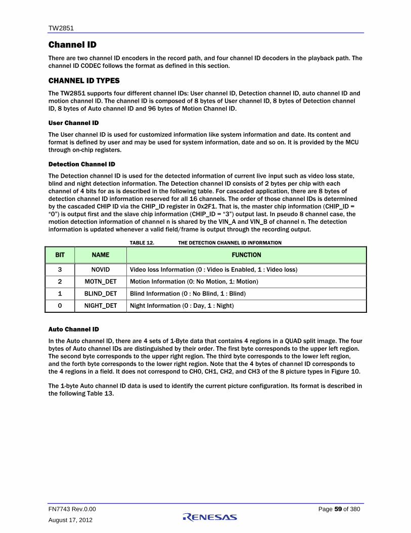
TW2851
FN7743 Rev.0.00 Page 59 of 380
August 17, 2012
Channel ID
There are two channel ID encoders in the record path, and four channel ID decoders in the playback path. The
channel ID CODEC follows the format as defined in this section.
CHANNEL ID TYPES
The TW2851 supports four different channel IDs: User channel ID, Detection channel ID, auto channel ID and
motion channel ID. The channel ID is composed of 8 bytes of User channel ID, 8 bytes of Detection channel
ID, 8 bytes of Auto channel ID and 96 bytes of Motion Channel ID.
User Channel ID
The User channel ID is used for customized information like system information and date. Its content and
format is defined by user and may be used for system information, date and so on. It is provided by the MCU
through on-chip registers.
Detection Channel ID
The Detection channel ID is used for the detected information of current live input such as video loss state,
blind and night detection information. The Detection channel ID consists of 2 bytes per chip with each
channel of 4 bits for as is described in the following table. For cascaded application, there are 8 bytes of
detection channel ID information reserved for all 16 channels. The order of those channel IDs is determined
by the cascaded CHIP ID via the CHIP_ID register in 0x2F1. That is, the master chip information (CHIP_ID =
“0”) is output first and the slave chip information (CHIP_ID = “3”) output last. In pseudo 8 channel case, the
motion detection information of channel n is shared by the VIN_A and VIN_B of channel n. The detection
information is updated whenever a valid field/frame is output through the recording output.
TABLE 12. THE DETECTION CHANNEL ID INFORMATION
BIT NAME FUNCTION
3 NOVID Video loss Information (0 : Video is Enabled, 1 : Video loss)
2 MOTN_DET Motion Information (0: No Motion, 1: Motion)
1 BLIND_DET Blind Information (0 : No Blind, 1 : Blind)
0 NIGHT_DET Night Information (0 : Day, 1 : Night)
Auto Channel ID
In the Auto channel ID, there are 4 sets of 1-Byte data that contains 4 regions in a QUAD split image. The four
bytes of Auto channel IDs are distinguished by their order. The first byte corresponds to the upper left region.
The second byte corresponds to the upper right region. The third byte corresponds to the lower left region,
and the forth byte corresponds to the lower right region. Note that the 4 bytes of channel ID corresponds to
the 4 regions in a field. It does not correspond to CH0, CH1, CH2, and CH3 of the 8 picture types in Figure 10.
The 1-byte Auto channel ID data is used to identify the current picture configuration. Its format is described in
the following Table 13.

TW2851
FN7743 Rev.0.00 Page 60 of 380
August 17, 2012
TABLE 13. AUTO CHANNEL ID BYTE 0 THROUGH BYTE 3 (FOR 4 REGIONS)
BIT NAME FUNCTION
7 PIC_TYPE[n] Picture Type bit n, located at bit 7 of byte n in auto channel ID bytes
6 STROBE STROBE represents a valid data in the specified channel window.
5 FLDMODE Sequence Unit (0: Frame, 1: Field) – Backward compatibility only
4 ANAPATH Analog switch information
[3:2] CASCADE Cascaded Stage Information – Backward compatibility only
[1:0] VIN_PATH Video Input Path Number
The bit 7 of auto-channel ID byte n is the bit n of PIC_TYPE. The PIC_TYPE is a code representing the picture
type described in Figure 1. The coding of PIC_TYPE[3:0] for each mode is shown in Table 14 below. The bit 6
is a STROBE used to denote the information update of each quad split area. If it is set to 1, then the video
data in the quad split area is valid to be used in CODEC or playback path. Otherwise, the quad split area is to
be ignored. The FLDMODE is used to denote the channel in the quad-split area is captured in either field or
frame format. This piece of information is redundant to the PIC_TYPE and can be derived from PIC_TYPE, as
shown in Table 14. The ANAPATH is used to identify the analog switch information of the channel in the quad
split area. The ANAPATH information is required for pseudo 8channel MUX application using analog switch.
The CASCADE is used to indicate the cascaded stage (chip ID) in chip-to-chip cascaded application. The
VIN_PATH information is used to indicate the video input channel.
TABLE 14. THE PICTURE TYPE CODE
CODE DESCRIPTION FLDMODE
0 D1 Field Mode 1
1 D1 Frame Mode 0
2 CIF Field Mode 1
3 CIF Frame Mode 0
4 CIF DVR Field Mode 1
5 CIF DVR Frame Mode 0
6 CIF Field Vx2 Mode 1
7 CIF DVR Vx2 Mode 1
8 Reserved n/a
9 4D1 Frame Mode 0
10 ~ 15 Reserved n/a

TW2851
FN7743 Rev.0.00 Page 61 of 380
August 17, 2012
The following figure shows the example of Auto channel ID for various recording picture types.
CH0
CH3
CH2
CH1
CH0
CH1
CH2
CH3
CH0
CH0
CH3CH2
CH1CH0
CH3CH2
CH1 A0 = “ 1100_0000
A1 = “ 1100_0001
A2 = “ 1100_0010
A3 = “ 1100_0011
A0 = “ 1110_0001
A1 = “ 1110_0010
A2 = “ 1110_0001
A3 = “ 1110_0010
CH2CH1
CIF Frame Mode
CIF Field Vx2 Mode
Auto Channel ID
Auto Channel ID
CH0
D1 Frame Mode
A0 = “1100_0000
A1 = “1100_0000
A2 = “1100_0000
A3 = “1100_0000
Auto Channel ID
CH0
D1 Field Mode
A0 = “ 1110_0000
A1 = “ 1110_0000
A2 = “ 1110_0000
A3 = “ 1110_0000
Auto Channel ID
CH3
CH0 CH0
CH3
CH0
CH3
CH2
CH1
CH0
CH1
CH2
CH3
CIF DVR Frame Mode
A0 = “ 1100_0000
A1 = “ 1100_0001
A2 = “ 1100_0010
A3 = “ 1100_0011
Auto Channel ID Auto Channel ID
A0 = “ 1110_0000
A1 = “ 1110_0000
A2 = “ 1110_0011
A3 = “ 1110_0011
CIF DVR Field Vx2 Mode
CH0
CH3CH2
CH1CH0
CH3CH2
CH1
CIF Field Mode
A0 = “ 1110_0000
A1 = “ 1110_0001
A2 = “ 1110_0010
A3 = “ 1110_0011
Auto Channel ID
CH0
CH3
CH2
CH1
CH0
CH1
CH2
CH3
CH0
CH3
CH2
CH1
CH0
CH1
CH2
CH3
CIF DVR Field Mode
A0 = “ 1110_0000
A1 = “ 1110_0001
A2 = “ 1110_0010
A3 = “ 1110_0011
Auto Channel ID
FIGURE 26. THE EXAMPLE OF AUTO CHANNEL ID FOR VARIOUS RECORD OUTPUT FORMATS
Motion Channel ID
The Motion Channel ID is used to carry 4 sets of the 16x12 motion flags (192 bits, or 24 bytes) for each quad
split regions on the field/frame picture. Similarly to the 4-byte of auto-channel ID, the first set of motion
channel ID corresponds to the upper left region, the second set upper right, the third set lower left, and the
fourth set lower right region. Total of 96 bytes of data are reserved in a motion channel ID. The motion
channel ID is sent through a digital type channel ID in the VBI only. The analog type does not carry motion
channel ID.
CHANNEL ID ENCODING SETTING
The TW2851 has several channel ID encoders to put the channel ID into the VBI of the multi-channel video
streams. The four types of channel IDs are embedded in the vertical blanking area in both analog and/or
digital formats. The digital format is mainly used for video compression CODEC connected through the
recording digital interface. The analog format is used if the recording device is an analog device such as a
VCR.
The use of the digital channel ID has priority over analog channel ID. The analog channel ID format encoding
is enabled via the ANA_ID_EN register and the digital type channel ID format encoding is operated via
DIG_ID_EN register. The motion channel information is enabled by MOTN_ID_EN. Within the analog channel
ID, each of the ID can be separately controlled by AUTO_ID_EN, DET_ID_EN, USER_ID_EN, ANA_RPT_EN, etc.
All these registers are at address 0x216 and 0x2A6.
In addition, there are registers used to control the format/location of the channel ID within the VBI. The
registers include the ANA_CHID_H_OFST (0x217, 0x2A7) to define horizontal start offset, the CHID_V_OFSTE
and CHID_V_OFSTO (0x21A, 0x21B, 0x2AA, 0x2AB) to define line offset between odd and even field, the
CHID_V_OFST (0x21A, 0x2AA) to define line offset for channel ID, and the ANA_CHID_BW (0x21B, 0x2AB) to
define pulse width for 1 bit data of analog channel ID. The magnitude of each bit is defined by the
ANA_CHID_HIGH / ANA_CHID_LOW (0x218, 0x219, 0x2A8, 0x2A9) register.
Figure 27 shows the relationship between channel ID and register setting in channel ID encoder.

TW2851
FN7743 Rev.0.00 Page 62 of 380
August 17, 2012
Run- In
ClockANA_CHID_H_OFST
ANA_CHID_BW
Parity
* Channel ID Type of each line can be detected with Channel ID Type
Auto channel ID (1 st 4 bytes) = 001
Auto channel ID (2 nd 4 bytes) = 010
Detection Channel ID = 011 / 100
User Channel ID = 101 / 110
Analog Channel ID Format
CHID_HIGH
Video Output
H
V
F
CHID_V_OFST +
CHID_V_OFSTO
A0 = 11000000 A1 = 11000001 A2 = 11000010 A2 = 11000010
Channel ID Type (*)
AUTO/DETECTION/USER
Digital Channel ID
User Channel ID
Detection Channel ID
Auto Channel ID
CHID_LOW
Motion Detection
Digital Channel ID
FIGURE 27. THE RELATED REGISTERS FOR CHANNEL ID ENCODING
CHANNEL ID DECODING SETTING
The TW2851 supports the channel ID decoder to detect/decode the digital/analog channel ID format during
VBI period. The decoding/detection of each channel ID detection can be enabled via the PBm_DID_EN,
PBm_AID_EN, and PBm_AUTO_CHID_DET registers at 0x12A ~ 0x13A.
Run- In
Clock
Parity
* Channel ID Type of each line can be detected with Channel ID Type
Auto channel ID = 001 / 010 (Repeated channel ID)
Detection Channel ID = 011 / 100
User Channel ID = 101 / 110
Analog Channel ID Format
CHID_MID_VAL
Video Output
H
V
F
CHID_V_OFST +
CHID_V_OFSTO
A0 = 11000000 A1 = 11000001 A2 = 11000010 A2 = 11000010
Channel ID Type (*)
AUTO/DETECTION/USER
Digital Channel ID
User Channel ID
Detection Channel ID
Auto Channel ID
ANA_CHID_BW
ANA_CHID_H_OFST
MOTION DETECTION
Digital Channel ID
FIGURE 28. THE RELATED REGISTERS FOR CHANNEL ID DECODING

TW2851
FN7743 Rev.0.00 Page 63 of 380
August 17, 2012
In order to provide accurate detection of analog channel ID decoder against noises from analog device such
as a VCR source, the channel ID LPF can be enabled via the PB_FLT_EN (0x12A, 0x13A) register. The
registers PB_CHID_MID_VAL (0x12E, 0x13E) are used to define the threshold level between high and low for
analog channel ID.
TW2851 channel ID decoder supports both automatic and manual channel ID detection modes to detect the
analog channel ID. In the automatic channel ID detection mode, the channel ID decoder identifies the analog
channel ID through a run-in clock embedded in the playback stream. The run-in clock insertion can be
specified via the PBm_RIC_EN (0x12A, 0x13A) registers. In the manual channel ID detection mode, the
decoder also use some preconfigured registers to specify the location of the analog channel ID, no matter the
playback stream has a run-in clock embedded or not. These registers include the PB_CHID_H_OFST (0x12C,
0x13C) to define horizontal start offset, the PB_CHID_FLD_OS (0x12A, 0x13A) to define line offset between
odd and even field, the PB_CHID_V_OFST (0x12B, 0x13B) to define line offset for channel ID, the
PB_CHID_LINE_SIZE (0x12B, 0x13B) to define how many lines of channel ID is inserted, and the
PB_ANA_CHID_BW (0x12D, 0x13D) to define pulse width for 1 bit data.
This decoded channel ID information can be read through the PB_CHID_TYPE (0x1A5) or PB_CHID_STATUS
registers (0x1A8 ~ 0x1AF). The PB_CHID_TYPE register specifies different types such as the Auto channel ID
(CHID_TYPE = “0”), or the detection/user channel ID (CHID_TYPE = “1”). The PB_CHn_AUTO_VLD (0x1A1),
DET_CHID_VLD, USER_CHID_VLD, MOTION_CHID_VLD (0x1A2) registers can be used to indicate whether the
auto channel ID, detection channel ID, user channel ID, and motion channel IDs are valid or not. In automatic
channel ID detection mode, the line size and bit width can be read through the PB_CHID_LINE_SIZE_DET and
PB_ANA_CHID_BW_DET (0x1A3) register. Figure 50 shows the relationship between channel ID and register
setting.
DIGITAL CHANNEL ID FORMAT
The four types of channel IDs are embedded in the vertical blanking area in both analog and/or digital
formats. The use of the digital channel ID has priority over analog channel ID. It is useful for DSP applications
to decode and extract the channel ID in digital format in just two lines of VBI. The digital channel ID is located
before the six analog channel ID lines.
There are two lines of digital channel ID defined in TW2851. The first line is for motion channel ID. It is used
to carry the motion detection flags of each channel. The second line is for auto/detection/user channel ID.
Its format is compatible with TW2835/TW2837 digital channel ID format. The two lines of digital channel ID
are located right before the analog channel ID. The register VIS_LINE_OS is used to determine the starting
line of the first line of digital channel ID. The analog channel lines is right after the second digital channel ID
line.
The First Digital Channel ID Line
The motion detection digital channel ID carries up to 4 channels of motion flags (16x12 bits or 24 bytes
each) within 1 digital channel ID line. Each channel corresponds to a quad split area on the window as was
the case of auto-channel ID. There are total of 96 bytes of motion flags information.
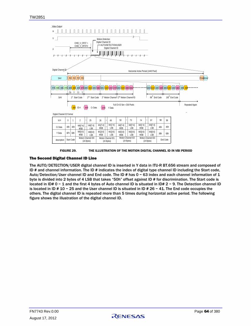
TW2851
FN7743 Rev.0.00 Page 64 of 380
August 17, 2012
Repeated Again
Cb Y Cr Y
Horizontal Active Period (1440 Pixel)Digital Channel ID
SAV EAVP0
80h 80h 40h 6Fh 80h 81h 40h 68h 80h 82h 4Xh 6Yh 80h 83h 4Mh 6Nh
P1
FFh 00h 00h XYh
P1440
1st Start Code 2nd Start Code 1st Motion Channel ID2nd Motion Channel ID
80h E2h 40h 68h
99th
End Code
80h E3h 40h 68h
100th
End Code
Full Ch ID Set = 256 Pixels
Digital Channel ID Format
~M0[7:4]
LSB
99
--
25~
Motion Channel ID0
(24 Bytes)
M0[7:4]
MSB
2
40h40hCr Data
End CodeStart Codedescription
9810Id #
00h 00h
80h ID # 4Xh Cr Data
SAV
P2 P3
Video Output
H
V
F
CHID_V_OFST +
CHID_V_OFSTO AUTO/DETECTION/USER
Digital Channel ID
Motion Detection
Digital Channel ID
~
49~
Motion Channel ID1
(24 Bytes)
26
~
73~
Motion Channel ID2
(24 Bytes)
50
~
97~
Motion Channel ID3
(24 Bytes)
74
40h
Y Data 6Fh 68h M0[3:0]
LSB
M0[3:0]
MSB
M1[7:4]
LSBM1[7:4]
MSB
M1[3:0]
LSB
M1[3:0]
MSB
M2[7:4]
LSBM2[7:4]
MSB
M2[3:0]
LSBM2[3:0]
MSB
M3[7:4]
LSB
M3[7:4]
MSB
M3[3:0]
LSB
M3[3:0]
MSB
40h
68h 68h
6Yh Y Data
FIGURE 29. THE ILLUSTRATION OF THE MOTION DIGITAL CHANNEL ID IN VBI PERIOD
The Second Digital Channel ID Line
The AUTO/DETECTION/USER digital channel ID is inserted in Y data in ITU-R BT.656 stream and composed of
ID # and channel information. The ID # indicates the index of digital type channel ID including the Start code,
Auto/Detection/User channel ID and End code. The ID # has 0 ~ 63 index and each channel information of 1
byte is divided into 2 bytes of 4 LSB that takes “50h” offset against ID # for discrimination. The Start code is
located in ID# 0 ~ 1 and the first 4 bytes of Auto channel ID is situated in ID# 2 ~ 9. The Detection channel ID
is located in ID # 10 ~ 25 and the User channel ID is situated in ID # 26 ~ 41. The End code occupies the
others. The digital channel ID is repeated more than 5 times during horizontal active period. The following
figure shows the illustration of the digital channel ID.

TW2851
FN7743 Rev.0.00 Page 65 of 380
August 17, 2012
Repeated Again
Cb Y Cr Y
Horizontal Active Period (1440 Pixel)Digital Channel ID
SAV EAVP0
80h 80h 40h 5Fh 80h 81h 40h 50h 80h 82h 40h 5Xh 80h 83h 40h 5Xh
P1
FFh 00h 00h XYh
P1440
1st Start Code 2nd Start Code 1st Auto Channel ID2nd Auto Channel ID
80h BEh 40h 50h
63th End Code
80h BFh 40h 50h
64th End Code
Full Ch ID Set = 256 Pixels
Digital Channel ID Format
~ {0101, U7_LSB}~
~
{ 0101, D7_LSB}~ {0101, A3_LSB}
63--25 ~
User Channel ID (8 Bytes)
{0101, U0_MSB}
26 41
Detection Channel ID (8 Bytes)
{0101, D0_MSB}
109~
Auto Channel ID (4 Bytes)
{0101, A0_MSB}
2
{0101, 0000}50h5FhData
End CodeStart Codedescription
4210Id #
00h 00h
80h ID # 5Xh Data
SAV
P2 P3
Video Output
H
V
F
CHID_V_OFST +
CHID_V_OFSTO AUTO/DETECTION/USER
Digital Channel ID
Motion Detection
Digital Channel ID
FIGURE 30. THE ILLUSTRATION OF THE AUTO/DETECTION/USER DIGITAL CHANNEL ID IN VBI PERIOD
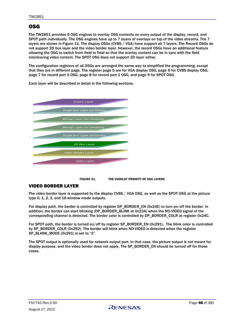
TW2851
FN7743 Rev.0.00 Page 66 of 380
August 17, 2012
OSG
The TW2851 provides 5 OSG engines to overlay OSG contents on every output of the display, record, and
SPOT path individually. The OSG engines have up to 7 layers of overlays on top of the video streams. The 7
layers are shown in Figure 11. The display OSGs (CVBS / VGA) have support all 7 layers. The Record OSGs do
not support 2D box layer and the video border layer. However, the record OSGs have an additional feature
allowing the OSG to switch from field to field so that the overlay content can be in sync with the field
interleaving video content. The SPOT OSG does not support 2D layer either.
The configuration registers of all OSGs are arranged the same way to simplified the programming, except
that they are in different page. The register page 5 are for VGA display OSG, page 6 for CVBS display OSG,
page 7 for record port 0 OSG, page 8 for record port 1 OSG, and page 9 for SPOT OSG.
Each layer will be described in detail in the following sections.
Cursor Layer
Single box Layer (x2 boxes)
Bitmap Layer (x1 windows)
Single box Layer (x6 boxes)
2D Box Layer
Video Border Layer
Video Layer
Bitmap Layer (x8 windows)
FIGURE 31. THE OVERLAY PRIORITY OF OSG LAYERS
VIDEO BORDER LAYER
The video border layer is supported by the display CVBS / VGA OSG, as well as the SPOT OSG at the picture
type 0, 1, 2, 3, and 16-window mode outputs.
For display path, the border is controlled by register DP_BORDER_EN (0x24E) to turn on/off the border. In
addition, the border can start blinking (DP_BORDER_BLINK at 0x23A) when the NO-VIDEO signal of the
corresponding channel is detected. The border color is controlled by DP_BORDER_COLR at register 0x24C.
For SPOT path, the border is turned on/off by register SP_BORDER_EN (0x291). The blink color is controlled
by SP_BORDER_COLR (0x292). The border will blink when NO-VIDEO is detected when the register
SP_BLANK_MODE (0x291) is set to “2”.
The SPOT output is optionally used for network output port. In that case, the picture output is not meant for
display purpose, and the video border does not apply. The SP_BORDER_EN should be turned off for those
cases.
TW2851
FN7743 Rev.0.00 Page 67 of 380
August 17, 2012
2-DIMENSIONAL ARRAYED BOX
The 2D arrayed boxes are mainly used to display the motion information, so the 2D boxes are available only
in the display VGA/CVBS output path. Corresponding to the 8 video windows in the display path, there are
eight 2D arrayed boxes to show the motion in the video windows. The 2D box OSG is tightly coupled with the
motion detection circuit in the front-end video decoder.
Since there are 8 2D-boxes, the configuration of each individual 2D-box is done through an indirect write
mechanism. The configuration register is applied to a specific 2D box if the corresponding bit in MDCH_SEL is
set to 1. For example, by setting MDCH_SEL[0] to 1, a write to MDBOX_EN at 0xm75 will turn on the
MDBOX_EN bit for the first 2D box. If MDCH_SEL is 0xFF, then a write to MDBOX_EN at 0xm75 will be set to
all 2D boxes simultaneously.
The 2D boxes can be used to make table menu or display motion detection information. The mode is set by
MDBOX_MODE (0xm84). In order to turn on a 2D box, a global MDBOX_EN at 0xm75 should be set to enable
the 2D box OSG. In addition, a register bit MDBOXn_EN (0xm85) is set to enable the specific 2D box out of
the 8 boxes. The 2D arrayed boxes have programmable number of row and column cells up to 16 x 16. It is
defined via the MDBOX_HCELL and MDBOX_VCELL (0xm8F). The horizontal and vertical location of left top is
controlled by the MDBOX_HOS and MDBOX_VOS (0xm87 ~ 0xm89). The horizontal and vertical size of each
cell is defined by the MDBOX_HW and MDBOX_VW (0xm8A ~ 0xm8C). The total size of 2D arrayed box will be
the same as the sum of cells in row and column. The border of 2D arrayed box can be enabled by the
MDBOX_BNDEN (0xm8D) register to show a color controlled via the MD_BNDRY_COLR (0xm8D) register
which selects one of 4 colors such as 0% black, 25% gray, 50% gray and 75% white.
The 2D arrayed box a mask plane and a detection plane. The mask plane is used to show the “masking” area
where the motion detection was not enabled. The detection plane represents the motion detected cell
excluding the mask cells among whole cells. Both the masking information and the motion information are
from the front-end motion detection circuit. The mask plane is enabled by the MDMASK_EN (0xm85) register
and the detection plane is enabled by the MDDET_EN (0xm85) register. The color of mask plane is controlled
by the MDMASK_COLR (0xm86) register and the color of detection plane is defined by the MDDET_COLR
(0xm86) register which selects one out of 12 fixed colors or 4 user defined colors using the CLUT (0xm78 ~
0xm83) registers. The plane can be transparently blended with video data by the MDBOX_MIX (0xm85) and
the alpha blending level is controlled as 25%, 50%, and 75% via the MDBOX_ALPHA (0xm75) register. Even
in the horizontal / vertical mirroring mode, the video data and motion detection result can be matched via
the MDBOX_HINV and MDBOX_VINV (0xm85) registers.
TW2851 provides a special function to indicate cursor cell inside 2D arrayed box. The cursor cell is enabled
by the MDCUR_EN (0xm85) register and the displayed location is defined by the MDCUR_HPOS and
MDCUR_VPOS (0xm8E) registers. Its color is a reverse color of cell boundary. It is useful function to control
motion mask region. The Figure 32 shows an example of 2D arrayed box in both table mode and motion
display mode.

TW2851
FN7743 Rev.0.00 Page 68 of 380
August 17, 2012
Detection Plane (MDMASK_EN = 0) : Color by MDDET_COLR
Boundary
MDBOX_HW
DBOX_HOS
MD
BO
X_V
OS
MD
BO
X_V
W
MD
BO
X_V
CE
LL =
4
MDBOX_HCELL = 7
Cursor Cell
MDCUR_HPOS = 5
MDCUR_VPOS = 1
Mask Plane (MDMASK_EN = 1) : Color by MDMASK_COLR Mask Plane
Boundary
Motion
detected
Cell
No Motion
Cell
MDBOX_HCELL = 15
MD
BO
X_
VC
EL
L =
11
Detection Plane
Table mode Motion display mode in MDDET_EN = 0
FIGURE 32. THE 2D ARRAYED BOX IN TABLE MODE AND MOTION DISPLAY MODE
BITMAP LAYER
Bitmap Buffer Structure
The TW2851 reserves a big space in the external DDR SDRAM for use by the bitmap layer. The bitmap buffer
is specified by a starting OSG_BASE address. For OSG write side, the base address is specified by
OSG_WRBASE_ADDR (0x641). At the read side, each of the 5 OSGs (display VGA, display CVBS, record, SPOT,
etc) has its own based address at 0xm36. The unit of the base addresses is 64 Kbytes. To avoid confusion,
all of these base addresses should be set to the same value. The bitmap buffer also has a register
OSG_MEM_WIDTH (0x640) to specify the bitmap buffer width, with the unit of 64 pixels. In this way, the
bitmap buffer is organized in a 2-dimensional space such that all the burst fill / burst move can be done with
respect to a 2-dimensional area, instead of a linear memory address. The internal format of bitmap buffer is
in either the 444 RGB format (565), or the 422 YUV format. The 444 RGB format is used only in the VGA /
LVDS path OSG. The 422 YUV format can be used in all OSGs, including display VGA/CVBS, record, spot, etc.
The use of bitmap buffer can be designed flexibly by the user. For example, some area can be assigned to be
used by VGA OSG, other area by record OSG, and yet other area used as scratch area for storing re-usable
font, logo, etc.
OSG Bitmap Preparation
The TW2851 provides various acceleration functions to allow the external MCU to upload/manipulate the
bitmap in the bitmap buffer efficiently.
Bitmap Burst Fill
The MCU can unload the bitmap into the bitmap buffer by specifying an area in the bitmap buffer, and
continuously write the pixel data into a register until the whole area is filled. To perform a bitmap burst fill,
the MCU will follow the procedure below.
Check whether there is a previously unfinished burst command by checking the OSG_OP_START register
(0x64F). If it is “1”, then the MCU will wait until it is cleared, i.e., previous command finished.
Set the OSG_OPMODE (0x642) to 0, which mean the bitmap burst fill mode.
Set the destination burst fill area in the bitmap buffer by setting OSG_DST_SV / OST_DST_SH (0x64B ~
0x64D) for the upper left corner, and OSG_DST_EV / OSG_DST_EH (0x648 ~ 0x64A) for the right lower
corner.
Set the OSG_OP_START to “1” to start a burst fill.

TW2851
FN7743 Rev.0.00 Page 69 of 380
August 17, 2012
Write a 64-byte of pixel data into data register (In either 8-bit or 16-bit per write, depending on the parallel
host interface data bus width)
Check the OSG_BMWR_BUSY (0x64F). If it is “1”, then repeat this step after a certain delay time.
Repeat (5) to (6) until the whole area is filled. After the whole burst fill is finished, the OSG_OP_START will be
cleared automatically to “0”.
Note that if the MCU supports the WAIT signal through the host interface, then step (6) is not needed. The
WAIT signal will automatically keep the MCU hardware interface waiting until the internal buffer is available
for MCU to fill 64 bytes of data.
Block Move
The MCU can move the bitmap from one area to another in the bitmap buffer by following the procedure
below.
Check whether there is a previously unfinished burst command by checking the OSG_OP_START register
(0x64F). If it is “1”, then the MCU will wait until it is cleared, i.e., previous command finished.
Set the OSG_OPMODE (0x642) to 1, which mean the bitmap block move mode.
Set the source location by setting the OSG_SRC_SH / OSG_SRC_SV in 0x645 ~ 0x647.
Set the destination block move area by setting OSG_DST_SV / OST_DST_SH (0x64B ~ 0x64D) for the upper
left corner, and OSG_DST_EV / OSG_DST_EH (0x648 ~ 0x64A) for the right lower corner.
Set the OSG_OP_START to “1” to start a block move. When the block move finishes, the OSG_OP_START bit
is self cleared to “0”.
Block Fill
The MCU can update a rectangular area of a single color by doing the following procedure.
Check whether there is a previously unfinished burst command by checking the OSG_OP_START register
(0x64F). If it is “1”, then the MCU will wait until it is cleared, i.e., previous command finished.
Set the OSG_OPMODE (0x642) to 2, which mean the bitmap burst fill mode.
Set the destination block move area by setting OSG_DST_SV / OST_DST_SH (0x64B ~ 0x64D) for the upper
left corner, and OSG_DST_EV / OSG_DST_EH (0x648 ~ 0x64A) for the right lower corner.
Set the color of the pixel in OSG_FILL_COLR (0x654 ~ 0x657). This is a 2-pixel data due to the use of 422
format in bitmap buffer.
Set the OSG_OP_START to “1” to start a block fill. When the block fill finishes, the OSG_OP_START bit is self
cleared to “0”
Color Conversion
TW2851 can convert a specific pixel data to another one during the bitmap fill, block move, block fill, and
upscaling operation. A color conversion table can be configured to specify 4 sets of source pixel data value
and destination pixel data value. Whenever a pixel data matches an entry in the color conversion table, its
pixel value is converted to the output pixel data before writing into the bitmap buffer. In order to do this,
simply turn on the color conversion by setting OSG_COLR_CON (0x642) to “1” before issuing the
OSG_OP_START in each of the operation.
TW2851 uses an indirect read/write mechanism to access internal color table. To access the color
conversion table,
Set the indirect target OSG_SELOSG (0x64E) to 0 to choose color conversion table

TW2851
FN7743 Rev.0.00 Page 70 of 380
August 17, 2012
Set the OSG_IND_ADDR (0x650) to the entry index to be accessed
Write the OSG_IND_WRDATA with the target data.
Issue OSG_INDRD / OSG_INDWR to read / write an entry. These bits are self-cleared after done. The address
will be auto-incremented. To continue write more entries, simply repeat step step (2) to (5).
The color conversion table has 4 entries of 8 bytes each. For the nth entry, (n = 0 ~ 3), the table address and
content is as follows
Byte 8*n + 0 input U
Byte 8*n + 1 input Y1
Byte 8*n + 2 input V
Byte 8*n + 3 input Y2
Byte 8*n + 4 output U
Byte 8*n + 5 output Y1
Byte 8*n + 6 output V
Byte 8*n + 7 output Y2
Bitmap Windows
The TW2851 OSG can display the content from any location/size in the bitmap buffer to any location on the
output video stream. The TW2851 supports two layers of bitmap OSG. One layer supports a single window up
to full screen size. Another layer supports 8 smaller non-overlapping windows. Each layer can be turned
on/off through register OSD_WINMAIN_ON and OSD_WINSUB_ON register in 0xm34. The bitmap pixel
format of YUV or RGB is also controlled in this register.
Each of the 9 windows can be further configured separately by first selecting the window number with
OSD_WINSEL in 0xm31. The OSD_WINSEL 0 ~ 7 are for the 8 windows of the multi-window layer, and 8 is the
window for the single window layer. Through this selection, the configuration changes are done by first writing
the configuration data in 0xm37 ~ 0xm3F, OSD_BLINK_EN (0xm30), and OSD_WIN_EN (0xm35), and then
issue a write command by setting OSD_WINSET bit to 1 in 0xm35. Through this, the configuration data of
each window is stored internally.
The setting of each window allows the bitmap layer controller to read an area of bitmap data from the
external DDR SDRAM, and display at a specified destination location on the screen. To do this, the source
OSG location is specified by OSD_SRC_SV and OSD_SRC_SH (0xm37 ~ 0xm39). There is a limitation on the
OSD_SRC_SH that it has to be at the 64 pixel boundary in order to display the OSG window correctly.
The destination area is specified by the upper left corner (OSD_DST_SV, OSD_DST_SH) and the lower right
corner (OSD_DST_EV, OSD_DST_EH) in register 0xm3A ~ 0xm3F, and also enable the window by setting the
enable bit OSD_WIN_EN (0xm35) to 1. Note that the implementation of TW2851 does not allow the 8
windows in the multi-window layer to overlap each other on the destination screen.
In addition to simply block read from the DDR SDRAM, each window also has the following features.
Transparent Blending
Each layer has its own transparent blending alpha so that the video / layer 1 and layer 2 can all be blended
together. The single window layer is control by OSD_GLOBAL_ALPHA1 (0xm32). The 8 windows in the 8-
window layer share another one OSD_GLOBAL_ALPHA2 (0xm33). The priority of the two layers can be
swapped, i.e., single window layer can be on top or bottom of the multi-window layer, by using the
OSD_BLEND_OPT at 0xm34.
Blinking
The 9 windows support the blinking feature independently. This is done by setting the OSD_BLINK_EN
(0xm30), and the bitmap will blink by switching on and off the bitmap window using a timer set by
OSD_BLINK_TIME (0xm35).
TW2851
FN7743 Rev.0.00 Page 71 of 380
August 17, 2012
Dynamic Field Switching
The recording path OSG features a dynamic field switching feature that allows the OSG windows be
controlled to turn on and off from field to field through the record switch queue entries. This mode is turned
on by setting OSD_WINSWITCH to 1. When this is set, the window enable signal is controlled by the record
switch queue entry. Bit 23 ~ 27 controls the lower 4 windows of OSG for record port 0, and bit 28 ~ bit 31
controls the lower 4 windows in the OSG of record port 1. When the switch queue entry changes from field to
field, the OSG windows enabled also changed. This allows an OSG window to lock on a particular channel in
the field interleaving case, and put on channel specific information. The upper 4 windows of the recording
path OSG are not affected by this setting.
SINGLE BOX
The TW2851 provides 8 single boxes that can be used for picture masking or drop down menu. The 8 single
boxes are separated into two layers. The first 2 windows are above the bitmap OSG layer, while the other 6
windows are below the bitmap OSG layer. Each of the layer can be turned on / off through the
BOX1D_EN[1:0] in 0xm67. Each layer can be programmed to blend transparently through BOX1D_ALPHA0
and BOX1D_ALPHA1 in 0xm64. Usually the single box is single color. When used as a picture privacy
masking box, however, the single box can be programmed to show mosaic blocks using two different colors.
The two colors are programmed through MOSAIC_COLOR_SEL0 and MOSAIC_COLOR_SEL1 at 0xm66.
Similar to the bitmap and 2D box layer, the 8 single boxes are programmed through indirect write by using
the MDCH_SEL in 0xm76. The configuration register is applied to a specific 1D box if the corresponding bit in
MDCH_SEL is set to 1. For example, by setting MDCH_SEL[0] to 1, a write to MOSAIC_EN at 0xm68 will turn
on the MOSAIC_EN bit for the first 1D box. If MDCH_SEL is 0xFF, then a write to MOSAIC_EN at 0xm67 will be
turn on the mosaic in all 2D boxes simultaneously.
The single box has configuration registers in register 0xm68 ~ 0xm6F. The BOX1D_HL is the horizontal
location of box with 2-pixel unit and the BOX1D_HW is the horizontal size of box with 2-pixel unit. The
BOX1D_VT is the vertical location of box with 1 line unit and the BOX1D_VW is the vertical size of box with 1
line unit. The BOX1D_BDR_EN and BOX1D_INT_EN (0xm68) registers turn on the border and interior display
of the 1D Box using the colors defined by BOX1D_COLR and BOX1D_BDR_COLR in 0xm69. The
BOX1D_COLR register selects one out of 12 fixed colors or 4 user defined colors specified with the CLUT
(0xm78 ~ 0xm83). The BOX1D_BDR_COLR selects one out of the 4 gray level colors.
In case that several boxes have same region, there will be a conflict of what to display for that region.
Generally the TW2851 defines that box 0 has priority over box 3. So if a conflict happens between more than
2 boxes, box 0 will be displayed first as top layer and box 1 to box 3 are hidden beneath.
MOUSE POINTER
The TW2851 supports the mouse pointers on all the 5 OSGs for display, record, and SPOT. However, only one
of them should be turned on at a time. This is through the CUR_EN in 0x65B. The mouse cursor supports
features such as reverse color, blinking, hollow shape, different size, or even custom cursor shape, all through
register 0x65C. The location of the cursor is at CUR_X, CUR_Y at 0x65D ~ 0x65F.
TW2851 supports customized cursor. The user can upload as many different cursor bitmaps as possible into
the external DDR memory through the DDR burst write through the host interface. Please refer to the Host
Interface section on page 87. The memory space used can be any area in the bitmap buffer, even though it is
not actually used by the bitmap OSG layer. The custom cursor is a bitmap of 48 x 48 pixels, with each pixel
represented in 2 bits. There will be total of 576 bytes of data for one customized cursor. The pixel
arrangement in the 576 bytes is big endian in rasterscan format. I.e., the first pixel is the bit [7:6] of byte 0,
second pixel is the bit [5:4] of byte 0, etc.,etc. The pixel data coding is as follows:
0 Transparent
1 border pixel (always black)
2 white pixel for interior
TW2851
FN7743 Rev.0.00 Page 72 of 380
August 17, 2012
3 black pixels for interior
Once all the cursors are uploaded in the DDR SDRAM, they can be read back on the fly into an on-chip cursor
RAM for use whenever needed. This is also done through the AUX interface.
(1) Enable the CUR_CUSTOM_LD bit to ‘1’
(2) Read the cursor content by setting the DDR AUX interface with size of 576 bytes. (Refer to the
Host Interface section on page 87.) The content will be burst read from the DDR to On-Chip cursor
SRAM. Note that with the setting of CUR_CUSTOM_LD in (1), the host burst interface automatically
read back the whole cursor bitmap continuously without CPU intervention. The MCU does not
need to read burst data like normal AUX read.
(3) Turn off the CUR_CUSTOM_LD by setting to ‘0’
(4) Set the CUR_SEL in 0x65C to 2 to use this custom cursor.

TW2851
FN7743 Rev.0.00 Page 73 of 380
August 17, 2012
Audio Codec
The audio codec in the TW2851 is composed of five audio Analog-to-Digital converters, 1 Digital-to-Analog
converter, audio mixer, digital serial audio interface and audio detector shown as the Figure 33. The TW2851
can accept 5 analog audio signals and 1 digital serial audio data and produce 1 mixing analog audio signal
and 2 digital serial audio data.
ADCAIN1 G
MIX
MUTE
ADCAIN2 G MUTE
ADCAIN3 G MUTE
MUTE
RATIO MUTE
I2S/DSP
Decoder
ACLKP
ASYNP
ADATP
ADCAIN4 G MUTE
ADCAIN51 G MUTE
I2S/DSP Encoder
ACLKR
ASYNR
ADATR
ADATM
Audio
Detector
Cascade In Mix
(AIN5 Pin Input)
PB1
PB3
PB4
PB2
AIN1 Digital
AIN2 Digital
AIN3 Digital
AIN4 Digital
AIN5 Digital
AIN6 Digital
AIN7 Digital
AIN8 Digital
AIN9 Digital
AIN10 Digital
AIN11 Digital
AIN12 Digital
AIN13 Digital
AIN14 Digital
AIN15 Digital
AIN16 Digital
AIN51 Digital
AIN52 Digital
AIN53 Digital
AIN54 Digital
OU
TP
UT
SE
LE
CT
AOUTDAC G
FIGURE 33. BLOCK DIAGRAM OF AUDIO CODEC
TW2851
FN7743 Rev.0.00 Page 74 of 380
August 17, 2012
The level of analog audio input signal AIN1 ~ AIN5 can be adjusted respectively by internal programmable
gain amplifiers that are defined via the AIGAIN1, AIGAIN2, AIGAIN3, AIGAIN4, and AIGAIN5 registers and
then sampled by each Analog-to-Digital converters. Figure 34 shows the audio decimation filter response. The
digital serial audio input data through the ACLKP, ASYNP and ADATP pin are used for playback function. To
record audio data, the TW2851 provides the digital serial audio output via the ACLKR, ASYNR and ADATR pin.
The TW2851 can mix all of audio inputs including analog audio signal and digital audio data according to the
predefined mixing ratio for each audio via the MIX_RATIO1 ~ MIX_RATIO5 and MIX_RATIOP registers. This
mixing audio output can be provided through the analog and digital interfaces. The ADATM pin supports the
digital mixing audio output and its digital serial audio timings are provided through the ACLKR and ASYNR
pins that are shared with the digital serial audio record timing pins.
(*) 0.016 line = 0.016x64xFs
FIGURE 34. AUDIO DECIMATION FILTER RESPONSE
AUDIO CLOCK MASTER/SLAVE MODE
The TW2851 has two types of Audio Clock modes. If ACLKRMASTER register is set to 1, the audio sample
rate 256xfs is processed from an internal audio clock generator ACKG. In this master mode, ACLKR/ASYNR
pins are output mode. ASYNROEN register for ASYNR pin should be set to 0 (output enable mode). If
ACLKRMASTER register is set to 0, audio sample rate is processed from external audio clock through the
ACLKR pin input. A 256xfs, 320xfs, or 384xfs external audio clock should be connected to ACLKR pin from
external master clock source in this slave mode. ASYNR pin can be input or output by external Audio clock
master in slave mode. ASYNR signal should change per fs audio sample rate in both master and slave mode.
AIN5MD and AFS384 register setup audio fs mode with the following table.

TW2851
FN7743 Rev.0.00 Page 75 of 380
August 17, 2012
REGISTER
FS MODE
AIN5MD AFS384
0 0 256xfs
1 0 320xfs
0 1 384xfs
AUDIO DETECTION
The TW2851 has an audio detector for each individual of 5 channels. There are 2 kinds of audio detection
method defined by the ADET_MTH. One is the detection of absolute amplitude and the other is of differential
amplitude. For both detection methods, the accumulating period is defined by the ADET_FILT register and the
detecting threshold value is defined by ADET_TH1 ~ ADET_TH5 registers. The status for audio detection is
read by the STATE_AVDET register and it also makes the interrupt request through the IRQ pin with the
combination of the status for video loss detection.
AUDIO MULTI-CHIP CASCADE
TW2851 can output 16 channel audio data on ACLKR/ASYNR/ADATR output simultaneously. Therefore, up
to 4 chips can be connected on most Multi-Chip application cases. ALINKI pin is the audio cascade serial
input, and ALINKO pin is the audio cascade serial output.
Each stage chip can accept 5 analog audio signals so that four cascaded chips will be 16-channel audio
controller as default AIN5MD=0. The first stage chip provides 16ch digital serial audio data for record. Even
though the first stage chip has only 1 digital serial audio data pin ADATR for record, the TW2851 can
generate 16 channel data simultaneously using multi-channel format. Also, each stage chip can support 4
channel record outputs that are corresponding with analog audio inputs. This first stage chip can also output
16 channels mixing audio data by the digital serial audio data and analog audio signal. The last stage chip
accepts the digital serial audio data for playback. The digital playback data can be converted to analog signal
by Digital-to-Analog Converter in the last stage chip.
In Multi-Chip Audio operation mode, one same Oscillator clock source (27 MHz) needs to be connected to all
TW2851 XTI or TW2851 CLKI pins.
Several Master/Slave mode configurations are available. The Figure 35 shows the most recommended and
demanded system with Clock Master mode (ACLKRMASTER=1). Figure 36 is the most recommended system
with Clock Slave Sync Slave mode (ACLKRMASTER=0, ASYNCR_OEN=1). Other system combinations are also
pissible if the application needs. The two cascade modes shown are typical systems.
In each of the following figures, Mix1-16-51-54/Pb1 means Mix output of AIN1-16, AIN51-AIN54, and
Playback1. AIN1-16-51-54/Pb1 means one selected Audio output in AIN1-16-51-54/Pb1.
If one TW2851 uses AIN5MD=1, all other cascaded TW2851 chips must set up AIN5MD=1 also. Generally, 4
audio input mode (AIN5MD=0) are most used in this cascade system.

TW2851
FN7743 Rev.0.00 Page 76 of 380
August 17, 2012
TW2851
First Stage
AOUT
IRQ
AOUT1
AIN1
AIN2
AIN3
AIN1
AIN2
AIN3
ACLKP
ASYNP
ADATP
ACLKR
ASYNR
ADATR
ADATM
ACLKR1
ASYNR1
ADATR1
ADATM1
XTI
ALINKO
ALINKI
Record Output
(AIN1-AIN16)
and
AIN51-54/Mix
Output
TW2851
Second StageAOUT
IRQAIN1
AIN2
AIN3
AIN4
AIN5
AIN6
AIN7
AIN8
ACLKP
ASYNP
ADATP
ACLKR
ASYNR
ADATR
ADATM
CLKI
ALINKO
ALINKI
TW2851
Third StageAOUT
IRQAIN1
AIN2
AIN3
AIN4
AIN9
AIN10
AIN11
AIN12
ACLKP
ASYNP
ADATP
ACLKR
ASYNR
ADATR
ADATM
CLKI
ALINKO
ALINKI
TW2851
Last Stage
AOUT
IRQAIN1
AIN2
AIN3
AIN4
AIN13
AIN14
AIN15
AIN16
ACLKP
ASYNP
ADATP
ACLKR
ASYNR
ADATR
ADATM
CLKI
ALINKO
ALINKI108MHz or
54MHz or
27MHzGND
Analog
Mix1-16-51-54-
Pb1/
AIN1-16-51-54/Pb1
Output
IRQ1
RSTB
RSTB
RSTB
RSTB RSTB
PCM/u-Law/A-Law/
Playback1 Input
PB1 ADATP
PB1 ACLKP
PB1 ASYNP
AIN4AIN4
AIN5AIN51
AIN5AIN52
AIN5AIN53
AIN5AIN54
FIGURE 35. RECOMMENDED CLOCK MASTER CASCADE MODE SYSTEM WITH ACLKRMASTER = 1; ASYNROEN = 0; PB_MASTER=0

TW2851
FN7743 Rev.0.00 Page 77 of 380
August 17, 2012
TW2851
First Stage
AOUT
IRQ
AOUT1
AIN1
AIN2
AIN3
AIN1
AIN2
AIN3
ACLKP
ASYNP
ADATP
ACLKR
ASYNR
ADATR
ADATM
ASYNR1 Fs Signal Input
ADATR1
ADATM1
XTI
ALINKO
ALINKI
Record Output
(AIN1-AIN16)
Mix/AIN51-54
Output
TW2851
Second StageAOUT
IRQAIN1
AIN2
AIN3
AIN4
AIN5
AIN6
AIN7
AIN8
ACLKP
ASYNP
ADATP
ACLKR
ASYNR
ADATR
ADATM
CLKI
ALINKO
ALINKI
TW2851
Third StageAOUT
IRQAIN1
AIN2
AIN3
AIN4
AIN9
AIN10
AIN11
AIN12
ACLKP
ASYNP
ADATP
ACLKR
ASYNR
ADATR
ADATM
CLKI
ALINKO
ALINKI
TW2851
Last StageAOUT
IRQAIN1
AIN2
AIN3
AIN4
AIN13
AIN14
AIN15
AIN16
ACLKP
ASYNP
ADATP
ACLKR
ASYNR
ADATR
ADATM
CLKI
ALINKO
ALINKI108MHz or
54MHz or
27MHzGND
Analog
Mix1-16-51-54-
Pb1/
AIN1-16-51-54/Pb1
Output
IRQ1
RSTB
RSTB
RSTB
RSTB RSTB
ACLKR
Clock-In
PCM/u-LAW/A-Law
Playback1 Input
PB1 ADATP
PB1 ACLKP
PB1 ASYNP
AIN4AIN4
AIN5AIN51
AIN5AIN52
AIN5AIN53
AIN5AIN54
FIGURE 36. RECOMMENDED CLOCK SLAVE SYNC SLAVE CASCADE MODE SYSTEM WITH ACLKRMASTER=0; ASYNROEN=1;
PB_MASTER=0
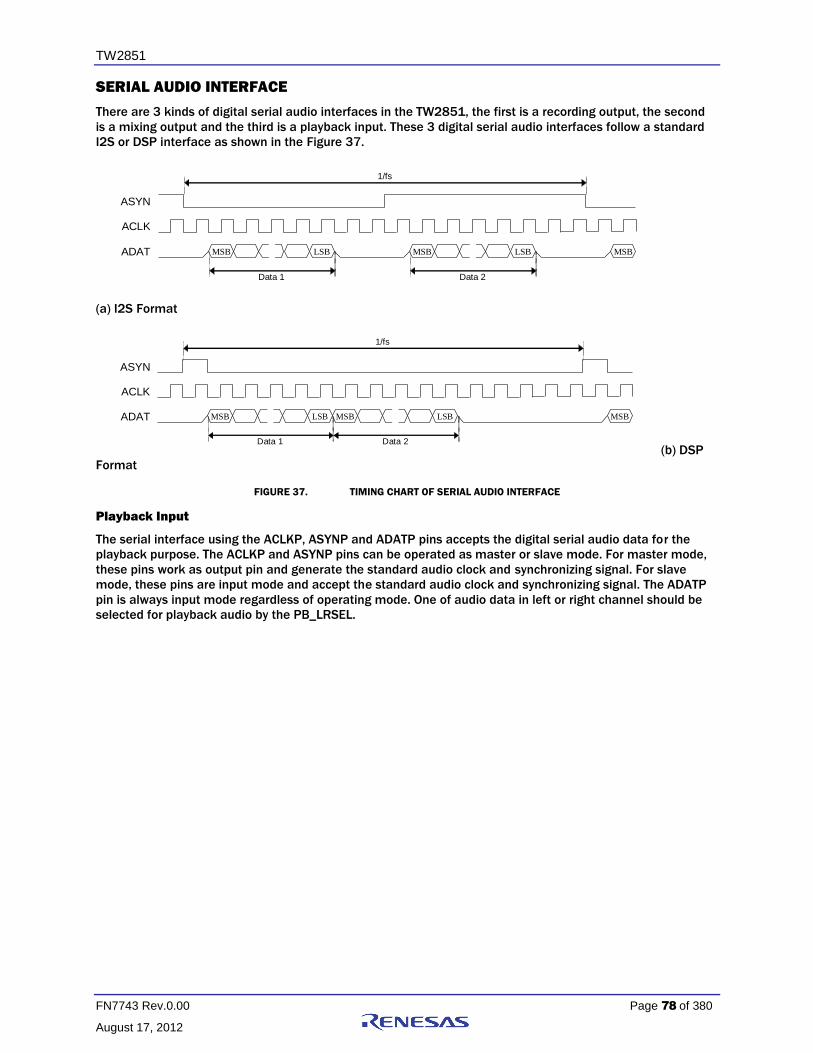
TW2851
FN7743 Rev.0.00 Page 78 of 380
August 17, 2012
SERIAL AUDIO INTERFACE
There are 3 kinds of digital serial audio interfaces in the TW2851, the first is a recording output, the second
is a mixing output and the third is a playback input. These 3 digital serial audio interfaces follow a standard
I2S or DSP interface as shown in the Figure 37.
MSB LSB MSB LSB MSB
1/fs
ASYN
ACLK
ADAT
Data 1 Data 2
(a) I2S Format
MSB LSB MSB LSB MSB
1/fs
ASYN
ACLK
ADAT
Data 1 Data 2 (b) DSP
Format
FIGURE 37. TIMING CHART OF SERIAL AUDIO INTERFACE
Playback Input
The serial interface using the ACLKP, ASYNP and ADATP pins accepts the digital serial audio data for the
playback purpose. The ACLKP and ASYNP pins can be operated as master or slave mode. For master mode,
these pins work as output pin and generate the standard audio clock and synchronizing signal. For slave
mode, these pins are input mode and accept the standard audio clock and synchronizing signal. The ADATP
pin is always input mode regardless of operating mode. One of audio data in left or right channel should be
selected for playback audio by the PB_LRSEL.
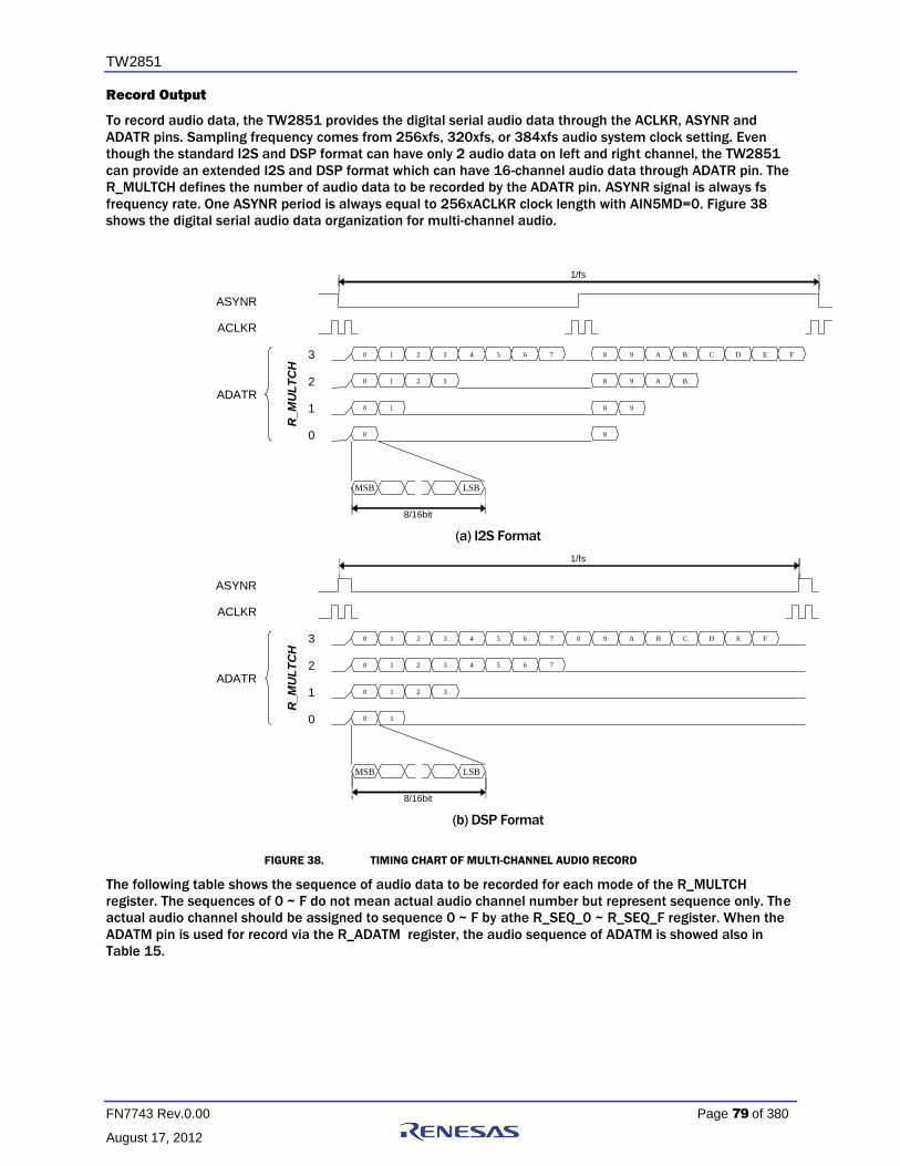
TW2851
FN7743 Rev.0.00 Page 79 of 380
August 17, 2012
Record Output
To record audio data, the TW2851 provides the digital serial audio data through the ACLKR, ASYNR and
ADATR pins. Sampling frequency comes from 256xfs, 320xfs, or 384xfs audio system clock setting. Even
though the standard I2S and DSP format can have only 2 audio data on left and right channel, the TW2851
can provide an extended I2S and DSP format which can have 16-channel audio data through ADATR pin. The
R_MULTCH defines the number of audio data to be recorded by the ADATR pin. ASYNR signal is always fs
frequency rate. One ASYNR period is always equal to 256xACLKR clock length with AIN5MD=0. Figure 38
shows the digital serial audio data organization for multi-channel audio.
0
1/fs
ASYNR
ACLKR
1 2 3 4 5 6 7 8 9 A B C D E F
0 1 2 3 8 9 A B
0 1 8 9
0 8
MSB LSB
8/16bit
ADATR
3
2
1
0
R_M
UL
TC
H
(a) I2S Format
0
1/fs
ASYNR
ACLKR
1 2 3 4 5 6 7 8 9 A B C D E F
0
ADATR
1 2 3 4 5 6 7
0 1 2 3
0 1
MSB LSB
8/16bit
3
2
1
0
R_M
UL
TC
H
(b) DSP Format
FIGURE 38. TIMING CHART OF MULTI-CHANNEL AUDIO RECORD
The following table shows the sequence of audio data to be recorded for each mode of the R_MULTCH
register. The sequences of 0 ~ F do not mean actual audio channel number but represent sequence only. The
actual audio channel should be assigned to sequence 0 ~ F by athe R_SEQ_0 ~ R_SEQ_F register. When the
ADATM pin is used for record via the R_ADATM register, the audio sequence of ADATM is showed also in
Table 15.

TW2851
FN7743 Rev.0.00 Page 80 of 380
August 17, 2012
TABLE 15. SEQUENCE OF MULTI-CHANNEL AUDIO RECORD
(A) I2S FORMAT
R_MULTCH Pin Left Channel Right Channel
0 ADATR 0 8 ADATM F 7
1 ADATR 0 1 8 9 ADATM F E 7 6
2 ADATR 0 1 2 3 8 9 A B ADATM F E D C 7 6 5 4
3 ADATR 0 1 2 3 4 5 6 7 8 9 A B C D E F
ADATM F E D C B A 9 8 7 6 5 4 3 2 1 0
(B) DSP FORMAT
R_MULTCH Pin Left/Right Channel
0 ADATR 0 1 ADATM F E
1 ADATR 0 1 2 3 ADATM F E D C
2 ADATR 0 1 2 3 4 5 6 7 ADATM F E D C B A 9 8
3 ADATR 0 1 2 3 4 5 6 7 8 9 A B C D E F
ADATM F E D C B A 9 8 7 6 5 4 3 2 1 0
Mix Output
The digital serial audio data on the ADATM pin has 2 different audio data which are mixing audio and
playback audio. The mixing digital serial audio data is the same as analog mixing output. The sampling
frequency, bit width and number of audio for the ADATM pin are same as the ADATR pin because the ACLKR
and ASYNR pins are shared with the ADATR and ADATM pins.

TW2851
FN7743 Rev.0.00 Page 81 of 380
August 17, 2012
AUDIO CLOCK SLAVE MODE DATA OUTPUT TIMING
TW2851 always output ASYNR/ADATR/ADATM by ACLKR falling edge triggered timing. ADATR/ADAMT
output data are always changing at the next ACLKR falling edge triggered timing after ASYNR signal changes.
If ASYNR is output, ADATR/ADATM outputs are always fixed to one ACLKR falling edge timing. But if ASYNR
is input, ADATR/ADATM output timing changes by ASYNR input timing.
ASYNR is ACLKR Falling Edge Triggered Input/output
If ASYNR is input and ASYNR input is ACLKR falling edge triggered input as ASYNR input signal is changing
after ACLKR falling edge, or if ASYNR is output, TW2851 output ADATR/ADATM by ACLKR falling edge
triggered timing as shown on following figures. ASYNR signal is changing during ACLKR = 0. TW2851 output
ADATR/ADATM data after next ACLKR falling edge triggered timing with more than half ACLKR clock delay.
MSB LSB MSB LSB MSB
1/fs
ASYNR
ACLKR
ADATR
Data 1 Data 2
FIGURE 39. AUDIO RECORD FALLING EDGE TRIGGERED INPUT/OUTPUT TIMING, ACLKMASTER=0, RM_SYNC=0
MSB LSB MSB LSB MSB
1/fs
ASYNR
ACLKR
ADATR
Data 1 Data 2
FIGURE 40. AUDIO RECORD FALLING EDGE TRIGGERED INPUT/OUTPUT TIMING, ACLKMASTER=0, RM_SYNC=1
ASYNR is ACLKR Rising Edge Triggered Input
If ASYNR is input and ASYNR input is ACLKR rising edge triggered input as ASYNR input signal is changing
after ACLKR rising edge, TW2851 output ADATR/ADATM by ACLKR falling edge triggered timing as shown on
following figures. ASYNR signal is changing during ACLKR = 1. TW2851 output ADATR/ADATM data after
next ACLKR falling edge triggered timing with less than half ACLKR clock delay.
MSB LSB MSB LSB MSB
1/fs
ASYNR
ACLKR
ADATR
Data 1 Data 2
FIGURE 41. AUDIO RECORD RISING EDGE TRIGGERED INPUT TIMING, ACLKMASTER=0, RM_SYNC=0, ASTBROEN=1

TW2851
FN7743 Rev.0.00 Page 82 of 380
August 17, 2012
MSB LSB MSB LSB MSB
1/fs
ASYNR
ACLKR
ADATR
Data 1 Data 2
FIGURE 42. AUDIO RECORD RISING EDGE TRIGGERED INPUT TIMING, ACLKMASTER=0, RM_SYNC=1, ASTBROEN=1
ACLKP/ASYNP SLAVE MODE DATA OUTPUT TIMING
The following 8 data input timing figures are supported. The ADATPDLY register needs to be set up according
to the difference of ADATP data input timings. Data1 is only used as default. MSB bit is the first input bit as
default PBINSWAP=0. If PBINSWAP=1, LSB bit is the first input bit.
ASYNP is ACLKP Falling Edge Triggered Input
MSB LSB MSB LSB MSB
1/fs
ASYNP
ACLKP
ADATP
Data 1 Data 2
FIGURE 43. AUDIO PLAYBACK FALLING EDGE TRIGGERED INPUT TIMING, RM_SYNC=0, PB_MASTER=0, ADATPDLY=0
MSB LSB MSB LSB MSB
1/fs
ASYNP
ACLKP
ADATP
Data 1 Data 2
FIGURE 44. AUDIO PLAYBACK FALLING EDGE TRIGGERED INPUT TIMING, RM_SYNC=1, PB_MASTER=0, ADATPDLY=0
MSB LSB MSB LSB MSB
1/fs
ASYNP
ACLKP
ADATP
Data 1 Data 2
FIGURE 45. AUDIO PLAYBACK FALLING EDGE TRIGGERED INPUT TIMING, RM_SYNC=0, PB_MASTER=0, ADATPDLY=1

TW2851
FN7743 Rev.0.00 Page 83 of 380
August 17, 2012
MSB LSB MSB LSB MSB
1/fs
ASYNR
ACLKR
ADATR
Data 1 Data 2
FIGURE 46. AUDIO PLAYBACK FALLING EDGE TRIGGERED INPUT TIMING, RM_SYNC=1, PB_MASTER=0, ADATPDLY=1
ASYNP is ACLKP Rising Edge Triggered Input
MSB LSB MSB LSB MSB
1/fs
ASYNP
ACLKP
ADATP
Data 1 Data 2
FIGURE 47. AUDIO PLAYBACK RISING EDGE TRIGGERED INPUT TIMING, RM_SYNC=0, PB_MASTER=0, ADATPDLY=1
MSB LSB MSB LSB MSB
1/fs
ASYNP
ACLKP
ADATP
Data 1 Data 2
FIGURE 48. AUDIO PLAYBACK RISING EDGE TRIGGERED INPUT TIMING, RM_SYNC=1, PB_MASTER=0, ADATPDLY=1
LSB LSB
1/fs
ASYNP
ACLKP
ADATP
Data 1 Data 2
MSB MSB
FIGURE 49. AUDIO PLAYBACK RISING EDGE TRIGGERED INPUT TIMING, RM_SYNC=0, PB_MASTER=0, ADATPDLY=0

TW2851
FN7743 Rev.0.00 Page 84 of 380
August 17, 2012
LSB MSB
1/fs
ASYNP
ACLKP
ADATP
Data 1 Data 2
MSBLSBMSB
FIGURE 50. AUDIO PLAYBACK RISING EDGE TRIGGERED INPUT TIMING, RM_SYNC=1, PB_MASTER=0, ADATPDLY=0
AUDIO CLOCK GENERATION
TW2851 has built-in field locked audio clock generator for use in video capture applications. The circuitry will
generate the same predefined number of audio sample clocks per field to ensure synchronous playback of
video and audio after digital recording or compression. The audio clock is digitally synthesized from the
crystal clock input. The master audio clock frequency is programmable through ACKN and ACKI register
based following two equations.
ACKN = round( F AMCLK / F field ), it gives the Audio master Clock Per Field.
ACKI = round( F AMCLK / F 27MHz * 2^23),it gives the Audio master Clock Nominal increment.
Following table provides setting example of some common used audio frequency assuming Video Decoder
system clock frequency of 27MHz. If ACLKRMASTER register bit is set to 1, following AMCLK is used as audio
system clock inside TW2851.
If Slave Playback-in lock mode is required,ACKN=00100hex and PBREFEN=1 needs to be set up. The number
of AMCLK clock per one ASYNP input cycle is locked(fixed) to 256 in this mode.
Frequency equation is “AMCLK(Freq) = 256 x ASYNP(Freq)”.
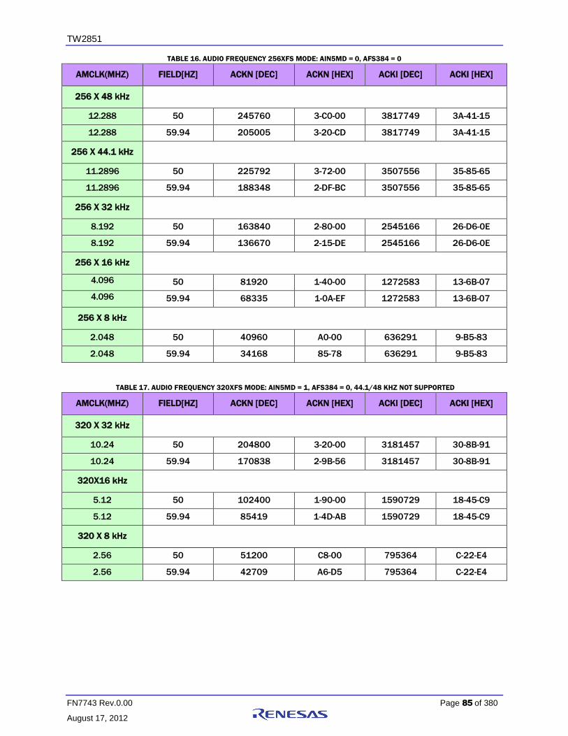
TW2851
FN7743 Rev.0.00 Page 85 of 380
August 17, 2012
TABLE 16. AUDIO FREQUENCY 256XFS MODE: AIN5MD = 0, AFS384 = 0
AMCLK(MHZ) FIELD[HZ] ACKN [DEC] ACKN [HEX] ACKI [DEC] ACKI [HEX]
256 X 48 kHz
12.288 50 245760 3-C0-00 3817749 3A-41-15
12.288 59.94 205005 3-20-CD 3817749 3A-41-15
256 X 44.1 kHz
11.2896 50 225792 3-72-00 3507556 35-85-65
11.2896 59.94 188348 2-DF-BC 3507556 35-85-65
256 X 32 kHz
8.192 50 163840 2-80-00 2545166 26-D6-0E
8.192 59.94 136670 2-15-DE 2545166 26-D6-0E
256 X 16 kHz
4.096 50 81920 1-40-00 1272583 13-6B-07
4.096 59.94 68335 1-0A-EF 1272583 13-6B-07
256 X 8 kHz
2.048 50 40960 A0-00 636291 9-B5-83
2.048 59.94 34168 85-78 636291 9-B5-83
TABLE 17. AUDIO FREQUENCY 320XFS MODE: AIN5MD = 1, AFS384 = 0, 44.1/48 KHZ NOT SUPPORTED
AMCLK(MHZ) FIELD[HZ] ACKN [DEC] ACKN [HEX] ACKI [DEC] ACKI [HEX]
320 X 32 kHz
10.24 50 204800 3-20-00 3181457 30-8B-91
10.24 59.94 170838 2-9B-56 3181457 30-8B-91
320X16 kHz
5.12 50 102400 1-90-00 1590729 18-45-C9
5.12 59.94 85419 1-4D-AB 1590729 18-45-C9
320 X 8 kHz
2.56 50 51200 C8-00 795364 C-22-E4
2.56 59.94 42709 A6-D5 795364 C-22-E4

TW2851
FN7743 Rev.0.00 Page 86 of 380
August 17, 2012
TABLE 18. AUDIO FREQUENCY 384XFS MODE: AIN5MD = 0, AFS384 = 1, 44.1/48 KHZ NOT SUPPORTED
AMCLK(MHZ) FIELD[HZ] ACKN [DEC] ACKN [HEX] ACKI [DEC] ACKI [HEX]
384 X 32 kHz
12.288 50 245760 3-C0-00 3817749 3A-41-15
12.288 59.94 205005 3-20-CD 3817749 3A-41-15
384X16 kHz
6.144 50 122880 1-E0-00 1908874 1D-20-8A
6.144 59.94 102503 1-90-67 1908874 1D-20-8A
384 X 8 kHz
3.072 50 61440 F0-00 954437 E-90-45
3.072 59.94 51251 C8-33 954437 E-90-45
AUDIO CLOCK AUTO SETUP
If ACLKRMASTER=1 audio clock master mode is selected,and AFAUTO register is set to “1”, TW2851 set up
ACKI register by AFMD register value automatically.ACKI control input in ACKG module block is automatically
set up to the required value by the condition of AIN5MD and AFS384 register value.
AFAUTO AFMD ACKG MODULE ACKI CONTROL INPUT VALUE
1 0 8kHz mode value by each AIN5MD/AFS384 case.
1 1 16kHz mode value by each AIN5MD/AFS384 case.
1 2 32kHz mode value by each AIN5MD/AFS384 case.
1 3 44.1kHz mode value by each AIN5MD/AFS384 case.
1 4 48kHz mode value by each AIN5MD/AFS384 case.
0 X ACKI register set up ACKI control input value.

TW2851
FN7743 Rev.0.00 Page 87 of 380
August 17, 2012
Host Interface
The TW2851 provides both serial and parallel interfaces that can be selected by HSP[1:0] pins. When HSP =
01, the I2C serial interface is selected. Else the parallel host interface is selected. There are three different
host interface mode: the address / data mux mode with ALE high active (HSP = 00), the address / data mux
mode with ALE low active (HSP = 10), and the address data separate mode (HSP = 11).
Some of the interface pins serve a dual purpose depending on the working mode. The pins HALE and HDAT
[7] in parallel mode become SCLK and SDAT pins in serial mode and the pins HDAT [6:1] and HCSB in
parallel mode become slave address in serial mode respectively. See Table 19 for pin assignment details of
each of the mode.
TABLE 19. PIN ASSIGNMENTS FOR SERIAL AND PARALLEL INTERFACE
PIN NAME SERIAL MODE
(HSP = 01)
A/D MUX WITH
HIGH ACTIVE ALE
(HSP = 00)
A/D MUX WITH
LOW ACTIVE ALE
(HSP = 10)
A / D SEPARATE
(HSP = 11)
HALE SCLK ALE ALE Not Used
HRDB Not Used (VSSO) RENB RENB RENB
HWRB Not Used (VSSO) WENB WENB WENB
HCSB Slave Address[0] CSB CSB CSB
HDAT[0] Not Used (VSSO) PDATA [0] /
PADDR[0]
PDATA[0] /
PADDR[0] PDATA[0]
HDAT[6:1] Slave Address[6:1] PDAT [6:1] /
PADDR[6:1]
PDAT [6:1] /
PADDR[6:1] PDATA[6:1]
HDAT[7] SDAT PDATA[7] /
PADDR[7]
PDATA[7] /
PADDR[7] PDATA[7]
HDAT[15:8] Not Used PDATA[15:8] PDATA[15:8] PDATA[15:8]
HADDR[7:0] Not Used Not Used Not Used PADDR[7:0]
HADDR[11:8] Not Used Not Used Not Used PADDR[11:8]
In serial interface mode and the A/D mux mode, the TW2851 has 8 bits of address. In order to access all the internal registers, an additional 4-bit address is used as page index. All the registers are organized into 16 page of 256 byte register each. The page index register is specified in a register at address 0xFF of each page. By setting the page index first, the following accesses are directed to the corresponding page. In cases of address / data separate mode, the page index is derived from PADDR[11:8]. The page index register at 0xFF is not used. For detailed description of registers, please refer to the

TW2851
FN7743 Rev.0.00 Page 88 of 380
August 17, 2012
Register Description section on page 97. In parallel bus case, the data bus width can be set to either 8-bit wide or 16-bit wide. This is controlled by a
power up strapping of the status of VGA_VS pin. If the VGA_VS pin is pull-up with an external resister, the
parallel interface data bus is 16-bit wide. If it is pull-down, then the data bus is 8-bit. All registers on TW2851
runs with 8-bit mode data bus only, except the OSD bitmap upload data register (0x652). This register can be
written 8-bit or 16-bit. Note that in some MCU running in 16-bit mode data bus, the addresses used to access
the registers on TW2851 need to be left shifted by 1 bit.

TW2851
FN7743 Rev.0.00 Page 89 of 380
August 17, 2012
SERIAL INTERFACE
HDAT [6:1] and HCSB pins define slave address in serial mode. Therefore, any slave address can be assigned
for full flexibility. The Figure 51 shows an illustration of serial interface for the case of slave address (Read :
“0x085”, Write : 0x084”).
FIGURE 51. THE SERIAL INTERFACE FOR THE CASE OF SLAVE ADDRESS. (READ : “0X085”, WRITE : “0X084”)
The detailed timing diagram is illustrated in Figure 52 and Figure 53.
MSB LSB MSB LSB MSB LSB
Start Slave address R/WB Ack Page index Ack Data Ack Stop
SDAT
SCLK
MSB LSB
Index address Ack
“0”
FIGURE 52. WRITE TIMING OF SERIAL INTERFACE
SDAT
SCLK
MSB LSB MSB LSB
Start Slave address R/WB Ack Index address Ack
MSB LSB MSB LSB
Start Slave address R/WB Data NoAck Stop
“0” “1”
Stop
Restart without stop is allowed
Index Write Procedure for Read Data Read Procedure
MSB LSB
Page Index Ack AckAck
MSB LSB
Data
FIGURE 53. READ TIMING OF SERIAL INTERFACE
SCLK
R20
1 4.7K
TW2851
U1
HCSB
HALE
HRDB HWRB
HDAT[7]
HDAT[6] HDAT[5] HDAT[4] HDAT[3]
HDAT[2]
HDAT[1]
HDAT[0]
3.3V/5V
R20
2 4.7K
R1
10
K
R20
0 10
K
3.3V/5V
Slave Address example Read : "10000101" Write : "10000100"
SDAT
3.3V/5V

TW2851
FN7743 Rev.0.00 Page 90 of 380
August 17, 2012
PARALLEL INTERFACE
For A/D Muxed parallel interface mode (HSP = 00 or 10), the address and data are multiplexed to share the
same bus pins. The writing and reading timing is shown in the Figure 54 and Figure 55 respectively. The
detail timing parameters are in Table 20.
TCS2CS
TCS2ALE TALE_W
TADDR_HTADDR_SETUPTCS2ADDR
ADDR WR_DATA
TALE2WR
TWDATA_H
HCSB
P_AD
ALE
HWRBTWR_W
TWDATA_SETUP
TWR2CS
FIGURE 54. WRITE TIMING OF PARALLEL INTERFACE WITH ADDRESS/DATA MULTIPLEXING MODE
TCS2CS
TCS2ALE TALE_W
TADDR_HTADDR_SETUPTCS2ADDR
ADDR RD_DATA
TRDATA_H
TALE2RD
HCSB
P_AD
ALE
HRDB
TRD_W
TRD2CS
TRD2DATA
FIGURE 55. READ TIMING OF PARALLEL INTERFACE WITH ADDRESS / DATA MULTIPLEXING MODE

TW2851
FN7743 Rev.0.00 Page 91 of 380
August 17, 2012
TABLE 20. TIMING PARAMETERS OF PARALLEL INTERFACE WITH ADDRESS / DATA MULTIPLEXING MODE
PARAMETER SYMBOL MIN TYP MAX UNITS
HCSB Setup Until ALE Active TCS2ALE > 0 ns
HCSB Setup Until ADDR Valid TCS2ADDR > 0 ns
ALE Active Pulse Width TALE_W 1 CPU_CLK
(Note 1) ns
ADDR Valid Until Inactive of ALE TADDR_SETUP 10 ns
ADDR Hold After ALE Inactive TADDR_H > 0 ns
ALE Inactive to HRDB Active TRD_W TRD2DATA ns
ALE Inactive to HWRB Active TWR_W 1 CPU_CLK
(Note 1) ns
Read DATA Hold After HRDB Inactive TRDATA_H > 0 ns
Write Data Hold After HWRB Inactive TWDATA_H > 0 Ns
HRDB Active Till Valid Read DATA TRD2DATA 30 ns
Write DATA Setup Before HWRB Active TWDATA_SETUP 10
HRDB Inactive Before HCSB Inactive TRD2CS > 0
HWRB Inactive Before HCSB Inactive TWR2CS 1 CPU_CLK
(Note 1)
HCSB Inactive Before HCSB Active TCS2CS 1 CPU_CLK
(Note 1) ns
NOTE:
1. The TW2851 internal CPU_CLK is 54 MHz
For the mode with HSP = 11, the address and data bus are separate. The ALE signal is not used. The read /
write timing of separate address/data bus is shown in Figure 56 and Figure 57.
TCS2CS
TWADDR_H
WR_DATA
TWDATA_H
HCSB
P_DATA
P_ADDR
HWRB
TWR_W
TWDATA_SETUP
ADDR
TWR2CS
TCS2WR
TWADDR_SETUP
FIGURE 56. WRITE TIMING OF PARALLEL INTERFACE WITH SEPARATE ADDRESS / DATA BUS

TW2851
FN7743 Rev.0.00 Page 92 of 380
August 17, 2012
TCS2CS
RD_DATA
TRDATA_HTCS2RD
HCSB
P_DATA
P_ADDR
HRDB
TRD_W
ADDR
TRD2CS
TRADDR_H
TRADDR_SETUP
TRD2DATA
FIGURE 57. READ TIMING OF PARALLEL INTERFACE WITH SEPARATE ADDRESS / DATA BUS
TABLE 21. TIMING PARAMETERS OF PARALLEL INTERFACE WITH SEPARATE ADDRESS / DATA BUS
PARAMETER SYMBOL MIN TYP MAX UNITS
HCSB Setup Until HWRB/HRDB
Active
TCS2RD
TCS2WR > 0 ns
Write ADDR Valid Until HWRB
Inactive TWADDR_SETUP 10 ns
Write ADDR Valid Until HRDB
Inactive TRADDR_SETUP 30 ns
Write ADDR Hold After HWRB
inactive TWADDR_H > 0 ns
Read ADDR Hold After HRDB
Inactive
TRADDR_H
> 0 ns
HRDB Active Pulse Width TRD_W TRD2DATA ns
HWRB Active Pulse Width TWR_W 1 CPU_CLK
(Note 1) ns
Read DATA Hold After HRDB
Inactive TRDATA_H > 0 ns
Write DATA Hold After HWRB
inactive TWDATA_H > 0 ns
Write DATA Setup Before HWRB
Inactive TWDATA_SETUP 10 ns
Read DATA Valid after ADDR Valid
and HRDB Active TRD2DATA
1 CPU_CLK +
30
(Note 1)
ns
HRDB / HWRB Inactive Before
HCSB Inactive
TRD2CS
TWR2CS > 0 ns
HCSB Active After HCSB Inactive TCS2CS 1 CPU_CLK
(Note 1) ns
NOTE:
1. The TW2851 internal CPU_CLK is 54 MHz

TW2851
FN7743 Rev.0.00 Page 93 of 380
August 17, 2012
VGA DDC I2C MASTER INTERFACE
The TW2851 provides an I2C master interface as DDC channel for the VGA interface. It allows the CPU to
read/write the DDC registers on the VGA monitors through this I2C interface. The DDC interface signals
DDC_CLK and DDC_DATA needs to be externally pulled up on the board. The DDC channel control registers
are at 0x9C0 ~ 0x9CF.
Before performing any of the I2C write/read operation, first program the DDC_CLK frequency by setting the
DDC_FREQ_DIV register (0x9C0 ~ 0x9C1). The DDC_CLK frequency is derived from an internal 54 MHz clock
divided by this parameter.
Write Operation
To write an I2C device through this I2C master interface,
1. Set the I2C slave device address and write command in DDC_WR_DATA register (0x9C2)
2. Write command 0x96 into register 0x9C4 DDC_COMMAND register. It will kick off the I2C Start
operation, and output the slave device address onto the DDC_DATA bus.
3. Wait for the ACK signal from I2C slave through the interrupt bit set in 0x9C4 DDC_STATUS register.
4. Clear the interrupt by writing 0x0F into DDC_COMMAND register (0x9C4)
5. Set the I2C slave register address in DDC_WR_DATA register (0x9C2)
6. Write command 0x16 to the DDC_COMMAND register (0x9C4) to put the address into SDA bus
7. Wait for the ACK signal as in (4)
8. Clear the interrupt as in (5)
9. Write the data to be written to I2C slave register in DDC_WR_DATA register (0x9C2)
10. Write command 0x16 to the DDC_COMMAND register (0x9C4) to put the data into SDA bus
11. Wait for ACK signal as in (4)
12. Clear the interrupt as in (5), and done with the I2C write operation
Read Operation
To read a register in I2C device through this I2C interface,
1. Write the I2C slave device address and read command into DDR_WR_DATA register (0x9C2)
2. Write 0x96 to DDC_COMMAND register to initiate the I2C Start operation, and put the slave device
address onto DDC_DATA bus
3. Wait for I2C slave ACK through the interrupt bit set in 0x9C4 DDC_STATUS register.
4. Clear the interrupt by writing 0x0F into DDC_COMMAND register (0x9C4)
5. Write the I2C slave register address into DDR_WR_DATA register (0x9C2)
6. Write 0x16 to DDC_COMMAND register to put the slave register address to DDC_DATA bus
7. Wait for I2C slave ACK as in (3)
8. Clear the interrupt as in (4)

TW2851
FN7743 Rev.0.00 Page 94 of 380
August 17, 2012
9. Write 0x26 into DDC_COMMAND register to urge the I2C slave to output the register data onto
DDC_DATA bus
10. Wait for the interrupt flag
11. Read the DDR_RD_DATA register 0x9C3 and finish the read operation
PS2 MOUSE INTERFACE
The TW2851 provides a PS2 interface for mouse support. With this, the CPU can receive interrupts whenever
the PS2 has events such as click, double click, cursor location change, etc. The PS2 interface signals PS2_CK
and PS2_D should be pulled up on the board. The PS2 control registers are at register 0x9D0 ~ 0x9DF.
INTERRUPT INTERFACE
The TW2851 provides the interrupt request function via an IRQ pin. Any video loss, motion, blind, and night
detection, status change, etc., will make IRQ pin low. There are total of 64 interrupt sources in TW2851, with
the INTERRUPT_VECT shown in register 0x1D0 to 0x1D7. Each bit of these registers represents one interrupt
source. To simplify the host polling effort, every 8 sources are further summarized in a second interrupt
status at register 0x1E0. In this status, if bit m is “1”, it means there are at least one source in 0x1Dm
triggered the IRQ pin. In order to clear the interrupt vector, simply write a “1” into the corresponding bit
location of the source into the INTERRUPT_VECT.
Associated with the 64 bit INTERRUPT_VECT, there are also 64 bit INTERRUPT_VECT_MASK that can be set to
“0” to mask out the interrupt source from triggering the IRQ pin. Note that this masking does not reset the
INTERRUPT_VECT. The host can still read the status of the masked sources from INTERRUPT_VECT.
For the list of interrupt sources corresponding to each of the INTERRUPT_VECT bit, please refer to the
description in the register description section.
BURST INTERFACE TO DDR SDRAM
TW2851 provides a burst circuit to allow CPU to burst read/write data from host interface to the external
DDR memory. This is useful for testing the external DDR memory. It is also used in writing the customized
cursor bitmap into DDR or reading the bitmap from DDR into the on-chip cursor SRAM.
To write data to DDR, do the following.
1. Write 0x2E0 / 0x2E1 / 0x2E2 with the DDR address to be accessed. The DDR address here is in
units of 2 bytes.
2. Write 0x2E3 / 0x2E4 with DMA length. This length can be 1 byte up to 1024 bytes. Internally, the
DDR burst is done 64 bytes by 64 bytes until it reaches the length specified here. The last burst can
be less than 64 bytes. The number of times the CPU writes in the last burst has to be exactly as
specified by this length. Note the DDR interface burst length is in unit of 4 bytes. So if the last DDR
burst length is not multiple of 4 bytes, the DDR still burst up to multiple of 4 bytes. Some garbage
data up to 3 bytes can be written into the DDR in the last DDR burst.
3. Write an AUX_DDR_WR command at 0x2E4 bit 0. This bit will be self cleared after done.
4. If the CPU parallel interface has P_WAIT signal, go ahead to start writing the 0x2DF address with the
data for AUX_DDR_LENGTH bytes. (This can be performed by the DMA engine at the CPU side).
5. If the CPU parallel interface has no P_WAIT signal, poll the AUX_FIFO_EMPTY bit at 0x2E4 bit 3. Wait
until this bit is set.
6. Repeat (4) or (5) as needed until total bytes up to the number specified previously in DMA length in
register 0x2E3/0x2E4. The last burst may be less than 64 bytes. After the last burst, the
AUX_DDR_WR command at 0x2E4 will be self-cleared. Note that before a full length is written, the
TW2851
FN7743 Rev.0.00 Page 95 of 380
August 17, 2012
CPU should not switch from write to read. Do not read 0x2DF until the burst write transaction is
done.
To read data from DDR, do the following:
1. Write 0x2E0 / 0x2E1 / 0x2E2 with the DDR address to be accessed. The DDR address here is in
units of 2 bytes.
2. Write 0x2E3 / 0x2E4 with DMA length. This length can be 1 byte up to 1024 bytes. Internally, the
DDR burst is done 64 bytes by 64 bytes until it reaches the length specified here. The last burst can
be less than 64 bytes. The number of times the CPU read in the last DDR burst has to exactly as
specified by this length.
3. Write an AUX_DDR_RD command at 0x2E4 bit 1. This bit will be self cleared after done.
4. If the CPU parallel interface has P_WAIT signal, go ahead to start reading the 0x2DF address with
the data for AUX_DDR_LENGTH bytes. (This can be performed by the DMA engine at the CPU side).
5. If the CPU parallel interface has no P_WAIT signal, poll the AUX_FIFO_FULL bit at 0x2E4 bit 2. Wait
until this bit is set, and proceed to read either 64 bytes (before the last DDR burst), or a length in the
last DDR burst consistent with the DMA length set in register 0x2E3/0x2E4.
6. Repeat (4) or (5) as needed.
Note that before a full length is read, the CPU should not switch from read to write. Do not write 0x2DF until
the burst read transaction is done.
External DRAM Interface
TW2851 uses a unified external DDR SDRAM for various functions, such as video buffers, bit-mapped OSG,
customized cursor bitmap, etc. The memory controller of the TW2851 supports 16bit data width up to 166
MHz clock rate. The memory capacity is 32 Mbytes.
When the chip is powered up, the CPU is responsible for setting all the on-chip configuration registers for DDR
memory configuration. Once the registers are set, the CPU releases the software reset signal, then the DDR
memory controller initializes the DDR memory configuration using the parameters in the registers. After the
initialization is done, the DDR memory is ready for use. After the initialization, the memory controller does
the memory refresh automatically.
Chip Reset / Initiation
TW2851 uses two reset signals: a hardware reset pin RST_N, and a software reset SOFT_RSTN register.
(0x2F0 bit 7). When the hardware reset RST_N pin is asserted, the whole chip is reset. When the software
reset register is asserted, the whole chip except all the on-chip configuration registers are reset. The content
in the on-chip register is not cleared by software reset. With this, TW2851 allows the micro-controller to first
release the hardware reset, and start configuring all the registers, and then release the software reset to start
normal operation.
In addition to the software reset, there is another register bit used for on-chip DLL reset. (0x2F0 bit 6) This
allows the CPU to control the on-chip DLL used by the DDR memory controller.
The programming sequence is as follows:
After PCB powered on, the hardware reset is released by hardware.
Initially the chip is in reset state. SOFT_RSTN (0x2F0 bit 7) is 0, DLL_RST (0x2F0 bit 6) is 1.
Release the DLL_RST afterward (Set DLL_RST to 1’b0).
Start configuring all the registers, especially the DDR configuration.

TW2851
FN7743 Rev.0.00 Page 96 of 380
August 17, 2012
Then released the SOFT_RSTN (Set SOFT_RSTN to 1’b1). After SOFT_RSTN is released, the DDR
controller start configuring the external DDR memory based on the setting in the register.
The chip is ready for normal operation.
Frequency Synthesizer Setup
There are three frequency synthesizers on TW2851. One is for DDR memory clock, one is for the VGA / LCD
panel clock, and the other is for generating the system clocks of 108 MHz. All the frequency synthesizers use
the same input clock (crystal or oscillator) of 27 MHz.
The frequency synthesizer for DDR memory clock generates a DDR clock of 166 MHz. The VGA clock depends
on the VGA resolution as defined in the VESA standard. The LCD panel clock depends on the make of the LCD
panel.
From the 27 MHz, an output clock frequency can be generated with the following equation.
Clock Frequency = 27 MHz x 2 x F [7:0]
R * NO
The Panel Clock configuration registers are at 0xEB0 ~ 0xEB2. The Memory Clock configuration registers are
at 0xEB4 ~ 0xEB6.
The third frequency synthesizer is a simpler one that only enhances the clock by 4X into 108 MHz. Other
video clocks such as 54 MHz, 27MHz, and 13.5 MHz are derived from 108 MHz.

TW2851
FN7743 Rev.0.00 Page 97 of 380
August 17, 2012
Register Description by Function
CVBS Video Input
VIDEO DECODER
# Address [7] [6] [5] [4] [3] [2] [1] [0]
0 0x000
VDLOSS* HLOCK* SLOCK* FLD* VLOCK* NOVIDEO* MONO* DET50* 1 0x010
2 0x020
3 0x030
* Read only bits
VDLOSS 1 Video not present. (Sync is not detected in number of
consecutive line periods specified by MISSCNT register)
0 Video detected.
HLOCK 1 Horizontal sync PLL is locked to the incoming video
source.
0 Horizontal sync PLL is not locked.
SLOCK 1 Sub-carrier PLL is locked to the incoming video source.
0 Sub-carrier PLL is not locked.
FLD 1 Even field is being decoded.
0 Odd field is being decoded.
VLOCK 1 Vertical logic is locked to the incoming video source.
0 Vertical logic is not locked.
NOVIDEO Reserved for TEST.
MONO 1 No color burst signal detected.
0 Color burst signal detected.
DET50 0 60Hz source detected
1 50Hz source detected
The actual vertical scanning frequency depends on the current
standard invoked.

TW2851
FN7743 Rev.0.00 Page 98 of 380
August 17, 2012
# Address [7] [6] [5] [4] [3] [2] [1] [0]
0 0x001
VCR* WKAIR* WKAIR1* VSTD* NINTL* VSHP 1 0x011
2 0x021
3 0x031
* Read only bits
VCR VCR signal indicator
WKAIR Weak signal indicator 2.
WKAIR1 Weak signal indicator controlled by WKTH
VSTD 1 = Standard signal
0 = Non-standard signal
NINTL 1 = Non-interlaced signal
0 = interlaced signal
VSHP Vertical Sharpness Control
0 = None (default)
7 = Highest
**Note: VSHP must be set to ‘0’ if COMB = 0
# Address [7] [6] [5] [4] [3] [2] [1] [0]
0 0x006
0 0 VACTIVE_
XY[8]
VDELAY_
XY[8] HACITIVE_XY[9:8] HDELAY_XY[9:8]
1 0x016
2 0x026
3 0x036
0 0x002
HDELAY_XY[7:0] 1 0x012
2 0x022
3 0x032
HDELAY_XY This 10bit register defines the starting location of horizontal active
pixel for display / record path. A unit is 1 pixel. The default value is
0x00F for NTSC and 0x00A for PAL.

TW2851
FN7743 Rev.0.00 Page 99 of 380
August 17, 2012
# Address [7] [6] [5] [4] [3] [2] [1] [0]
0 0x006
0 0 VACTIVE_
XY[8]
VDELAY_
XY[8] HACITIVE_XY[9:8] HDELAY_XY[9:8]
1 0x016
2 0x026
3 0x036
0 0x003
HACTIVE_XY[7:0] 1 0x013
2 0x023
3 0x033
HACTIVE_XY This 10bit register defines the number of horizontal active pixel for
display / record path. A unit is 1 pixel. The default value is decimal
720.
# Address [7] [6] [5] [4] [3] [2] [1] [0]
0 0x006
0 0 VACTIVE_
XY[8]
VDELAY_
XY[8] HACITIVE_XY[9:8] HDELAY_XY[9:8]
1 0x016
2 0x026
3 0x036
0 0x004
VDELAY_XY[7:0] 1 0x014
2 0x024
3 0x034
VDELAY_XY This 9bit register defines the starting location of vertical active for
display / record path. A unit is 1 line. The default value is decimal
6.
# Address [7] [6] [5] [4] [3] [2] [1] [0]
0 0x006
0 0 VACTIVE_
XY[8]
VDELAY_
XY[8] HACITIVE_XY[9:8] HDELAY_XY[9:8]
1 0x016
2 0x026
3 0x036
0 0x005
VACTIVE_XY[7:0] 1 0x015
2 0x025
3 0x035
VACTIVE_XY This 9bit register defines the number of vertical active lines for
display / record path. A unit is 1 line. The default value is decimal
240.

TW2851
FN7743 Rev.0.00 Page 100 of 380
August 17, 2012
# Address [7] [6] [5] [4] [3] [2] [1] [0]
0 0x007
HUE 1 0x017
2 0x027
3 0x037
HUE These bits control the color hue as 2's complement number. They
have value from +36o (7Fh) to -36o (80h) with an increment of 2.8o.
The 2 LSB has no effect. The positive value gives greenish tone and
negative value gives purplish tone. The default value is 0o (00h).
This is effective only on NTSC system. The default is 00h.
# Address [7] [6] [5] [4] [3] [2] [1] [0]
0 0x008
SCURVE VSF CTI SHARPNESS 1 0x018
2 0x028
3 0x038
SCURVE This bit controls the center frequency of the peaking filter. The
corresponding gain adjustment is HFLT.
0 Low
1 center
VSF This bit is for internal used. The default is 0.
CTI CTI level selection. The default is 1.
0 None
3 Highest
SHARPNESS These bits control the amount of sharpness enhancement on the
luminance signals. There are 16 levels of control with ‘0’ having no
effect on the output image. 1 through 15 provides sharpness
enhancement with ‘F’ being the strongest. The default is 1.
# Address [7] [6] [5] [4] [3] [2] [1] [0]
0 0x009
CNTRST 1 0x019
2 0x029
3 0x039
CNTRST These bits control the luminance contrast gain. A value of 100
(64h) has a gain of 1. The range adjustment is from 0% to 255% at
1% per step. The default is 64h.

TW2851
FN7743 Rev.0.00 Page 101 of 380
August 17, 2012
VIN Address [7] [6] [5] [4] [3] [2] [1] [0]
0 0x00A
BRIGHT 1 0x01A
2 0x02A
3 0x03A
BRIGHT These bits control the brightness. They have value of –128 to 127
in 2's complement form. Positive value increases brightness. A
value 0 has no effect on the data. The default is 00h.
# Address [7] [6] [5] [4] [3] [2] [1] [0]
0 0x00B
SAT_U 1 0x01B
2 0x02B
3 0x03B
SAT_U These bits control the digital gain adjustment to the U (or Cb)
component of the digital video signal. The color saturation can be
adjusted by adjusting the U and V color gain components by the
same amount in the normal situation. The U and V can also be
adjusted independently to provide greater flexibility. The range of
adjustment is 0 to 200%. A value of 128 (80h) has gain of 100%.
The default is 80h.
# Address [7] [6] [5] [4] [3] [2] [1] [0]
0 0x00C
SAT_V 1 0x01C
2 0x02C
3 0x03C
SAT_V These bits control the digital gain adjustment to the V (or Cr)
component of the digital video signal. The color saturation can be
adjusted by adjusting the U and V color gain components by the
same amount in the normal situation. The U and V can also be
adjusted independently to provide greater flexibility. The range of
adjustment is 0 to 200%. A value of 128 (80h) has gain of 100%.
The default is 80h.
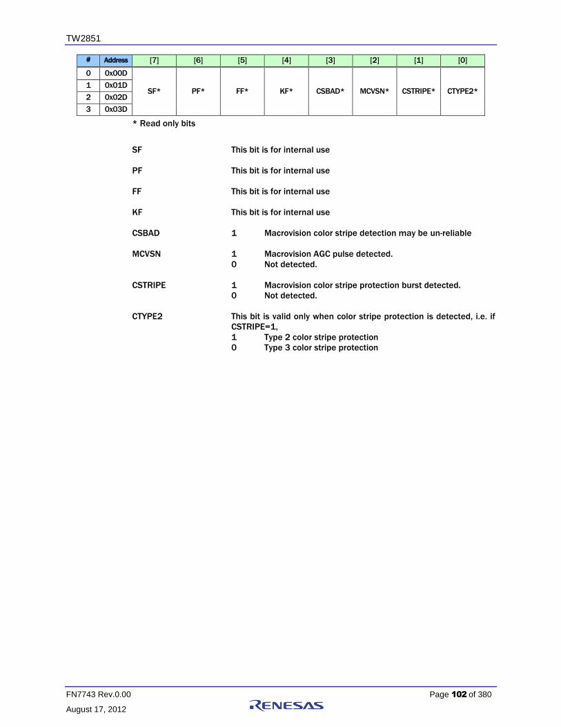
TW2851
FN7743 Rev.0.00 Page 102 of 380
August 17, 2012
# Address [7] [6] [5] [4] [3] [2] [1] [0]
0 0x00D
SF* PF* FF* KF* CSBAD* MCVSN* CSTRIPE* CTYPE2* 1 0x01D
2 0x02D
3 0x03D
* Read only bits
SF This bit is for internal use
PF This bit is for internal use
FF This bit is for internal use
KF This bit is for internal use
CSBAD 1 Macrovision color stripe detection may be un-reliable
MCVSN 1 Macrovision AGC pulse detected.
0 Not detected.
CSTRIPE 1 Macrovision color stripe protection burst detected.
0 Not detected.
CTYPE2 This bit is valid only when color stripe protection is detected, i.e. if
CSTRIPE=1,
1 Type 2 color stripe protection
0 Type 3 color stripe protection

TW2851
FN7743 Rev.0.00 Page 103 of 380
August 17, 2012
# Address [7] [6] [5] [4] [3] [2] [1] [0]
0 0x00E
DETSTUS*
STDNOW*
ATREG
STANDARD
1 0x01E
2 0x02E
3 0x03E
* Read only bits
DETSTUS 0 Idle
1 detection in progress
STDNOW Current standard invoked
0 NTSC(M)
1 PAL (B,D,G,H,I)
2 SECAM
3 NTSC4.43
4 PAL (M)
5 PAL (CN)
6 PAL 60
7 Not valid
ATREG 1 Disable the shadow registers
0 Enable VACTIVE and HDELAY shadow registers value
depending on STANDARD. (Default)
STANDARD Standard selection
0 NTSC(M)
1 PAL (B,D,G,H,I)
2 SECAM
3 NTSC4.43
4 PAL (M)
5 PAL (CN)
6 PAL 60
7 Auto detection (Default)

TW2851
FN7743 Rev.0.00 Page 104 of 380
August 17, 2012
# Address [7] [6] [5] [4] [3] [2] [1] [0]
0 0x00F
ATSTART PAL60EN PALCNEN PALMEN NTSC44EN SECAMEN PALBEN NTSCEN 1 0x01F
2 0x02F
3 0x03F
ATSTART 1 Writing 1 to this bit will manually initiate the auto format
detection process. This bit is a self-clearing bit
0 Manual initiation of auto format detection is done.
(Default)
PAL60EN 1 Enable recognition of PAL60 (Default)
0 Disable recognition
PALCNEN 1 Enable recognition of PAL (CN). (Default)
0 Disable recognition
PALMEN 1 Enable recognition of PAL (M). (Default)
0 Disable recognition
NTSC44EN 1 Enable recognition of NTSC 4.43. (Default)
0 Disable recognition
SECAMEN 1 Enable recognition of SECAM. (Default)
0 Disable recognition
PALBEN 1 Enable recognition of PAL (B,D,G,H,I). (Default)
0 Disable recognition
NTSCEN 1 Enable recognition of NTSC (M). (Default)
0 Disable recognition
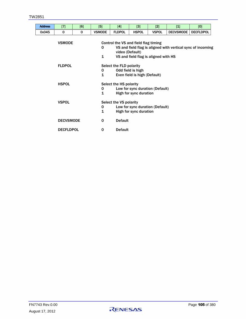
TW2851
FN7743 Rev.0.00 Page 105 of 380
August 17, 2012
Address [7] [6] [5] [4] [3] [2] [1] [0]
0x045 0 0 VSMODE FLDPOL HSPOL VSPOL DECVSMODE DECFLDPOL
VSMODE Control the VS and field flag timing
0 VS and field flag is aligned with vertical sync of incoming
video (Default)
1 VS and field flag is aligned with HS
FLDPOL Select the FLD polarity
0 Odd field is high
1 Even field is high (Default)
HSPOL Select the HS polarity
0 Low for sync duration (Default)
1 High for sync duration
VSPOL Select the VS polarity
0 Low for sync duration (Default)
1 High for sync duration
DECVSMODE 0 Default
DECFLDPOL 0 Default

TW2851
FN7743 Rev.0.00 Page 106 of 380
August 17, 2012
Address [7] [6] [5] [4] [3] [2] [1] [0]
0x046 AGCEN4 AGCEN3 AGCEN2 AGCEN1 AGCGAIN4[8] AGCGAIN3[8] AGCGAIN2[8] AGCGAIN1[8]
0x047 AGCGAIN1[7:0]
0x048 AGCGAIN2[7:0]
0x049 AGCGAIN3[7:0]
0x04A AGCGAIN4[7:0]
AGCENn Select Video AGC loop function on VIN of channel n
0 AGC loop function enabled (recommended for most
application cases) (default).
1 AGC loop function disabled. Gain is set by AGCGAINn
AGCGAINn These registers control the AGC gain of channel n when AGC loop is
disabled. Default value is 0F0h.
Address [7] [6] [5] [4] [3] [2] [1] [0]
0x04B PD_BIAS V_ADC_SAVE 0 0 0 YFLEN
PD_BIAS 1 Power down the bias of all 4 VADC
0 Do not power down the bias
V_ADC_SAVE Power Saving Mode Selection.
0 Most Power Consuming
7 Most Power Saving
IREF 0 Internal current reference 1 for Video ADC (default)
1 Internal current reference increase 30% for Video ADC.
VREF 0 Internal voltage reference for Video ADC (default)
1 Internal voltage reference shut down for Video ADC
YFLEN Analog Video CH1/CH2/CH3/CH4 anti-alias filter control
1 Enable(default)
0 Disable

TW2851
FN7743 Rev.0.00 Page 107 of 380
August 17, 2012
Address [7] [6] [5] [4] [3] [2] [1] [0]
0x04D TST_ADC_VD1 ADC_SEL1 0 0 0 0
TST_ADC_VD1 0 Default
ADC_SEL1 0 Default
Address [7] [6] [5] [4] [3] [2] [1] [0]
0x04E TST_ADC_VD2 ADC_SEL2 0 0 0 0
TST_ADC_VD2 0 Default
ADC_SEL2 0 Default
Address [7] [6] [5] [4] [3] [2] [1] [0]
0x04F FRM YNR CLMD PSP
FRM Free run mode control
0 Auto(default)
2 Default to 60Hz
3 Default to 50Hz
YNR Y HF noise reduction
0 None(default)
1 Smallest
2 Small
3 Medium
CLMD Clamping mode control
0 Sync top
1 Auto(default)
2 Pedestal
3 N/A
PSP Slice level control
0 Low
1 Medium(default)
2 High

TW2851
FN7743 Rev.0.00 Page 108 of 380
August 17, 2012
Address [7] [6] [5] [4] [3] [2] [1] [0]
0x050 HFLT2 HFLT1
0x051 HFLT4 HFLT3
HFLTn HFLTn controls the peaking function of channel n. Reserved for test
purpose.
Address [7] [6] [5] [4] [3] [2] [1] [0]
0x052 CTEST YCLEN 0 AFLTEN GTEST VLPF CKLY CKLC
CTEST Clamping control for debugging use. (Test purpose only)
(default 0)
YCLEN 1 Y channel clamp disabled (Test purpose only)
0 Enabled (default)
AFLTEN 1 Analog Audio input Anti-Aliasing Filter enabled (default)
0 Disabled
GTEST 1 Test (Test purpose only)
0 Normal operation (default)
VLPF Clamping filter control (default 0)
CKLY Clamping current control 1 (default 0)
CKLC Clamping current control 2 (default 0)
Address [7] [6] [5] [4] [3] [2] [1] [0]
0x053 NT502 NT501
NT501 1 Force the Video Decoder 1 to a special NTSC 50 Hz
format
0 Do not force to NTSC 50 Hz format
NT502 1 Force the Video Decoder 2 to a special NTSC 50 Hz
format
0 Do not force to NTSC 50 Hz format
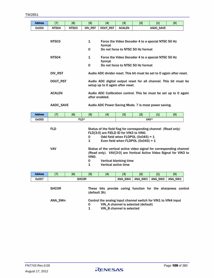
TW2851
FN7743 Rev.0.00 Page 109 of 380
August 17, 2012
Address [7] [6] [5] [4] [3] [2] [1] [0]
0x054 NT504 NT503 DIV_RST DOUT_RST ACALEN AADC_SAVE
NT503 1 Force the Video Decoder 4 to a special NTSC 50 Hz
format
0 Do not force to NTSC 50 Hz format
NT504 1 Force the Video Decoder 4 to a special NTSC 50 Hz
format
0 Do not force to NTSC 50 Hz format
DIV_RST Audio ADC divider reset. This bit must be set to 0 again after reset.
DOUT_RST Audio ADC digital output reset for all channel. This bit must be
setup up to 0 again after reset.
ACALEN Audio ADC Calibration control. This be must be set up to 0 again
after enabled.
AADC_SAVE Audio ADC Power Saving Mode. 7 is most power saving.
Address [7] [6] [5] [4] [3] [2] [1] [0]
0x055 FLD* VAV*
FLD Status of the field flag for corresponding channel (Read only)
FLD[3:0] are FIELD ID for VIN3 to VIN0.
0 Odd field when FLDPOL (0x045) = 1
1 Even field when FLDPOL (0x045) = 1
VAV Status of the vertical active video signal for corresponding channel
(Read only). VAV[3:0] are Vertical Active Video Signal for VIN3 to
VIN0.
0 Vertical blanking time
1 Vertical active time
Address [7] [6] [5] [4] [3] [2] [1] [0]
0x057 SHCOR ANA_SW4 ANA_SW3 ANA_SW2 ANA_SW1
SHCOR These bits provide coring function for the sharpness control
(default 3h)
ANA_SWn Control the analog input channel switch for VIN1 to VIN4 input
0 VIN_A channel is selected (default)
1 VIN_B channel is selected

TW2851
FN7743 Rev.0.00 Page 110 of 380
August 17, 2012
Address [7] [6] [5] [4] [3] [2] [1] [0]
0x058 PBW DEM PALSW SET7 COMB HCOMP YCOMB PDLY
PBW 1 Wide Chroma BPF BW (Default)
0 Normal Chroma BPF BW
DEM Reserved (Default 1)
PALSW 1 PAL switch sensitivity low.
0 PAL switch sensitivity normal (Default)
SET7 1 The black level is 7.5 IRE above the blank level.
0 The black level is the same as the blank level (Default)
COMB 1 Adaptive comb filter for NTSC and PAL
(Recommended). This setting is not for SECAM (Default)
0 Notch filter. For SECAM, always set to 0.
HCOMP 1 Operation mode 1 (Recommended) (Default)
0 Mode 0
YCOMB 1 Bypass Comb filter when no burst presence
0 No bypass (Default)
PDLY 0 Enable PAL delay line (default)
1 Disable PAL delay line
Address [7] [6] [5] [4] [3] [2] [1] [0]
0x059 GMEN CKHY HSDLY
GMEN Reserved (Default 0)
CKHY Color killer hysteresis.
0 Fastest (Default)
1 Fast
2 Medium
3 Slow
HSDLY Reserved for test

TW2851
FN7743 Rev.0.00 Page 111 of 380
August 17, 2012
Address [7] [6] [5] [4] [3] [2] [1] [0]
0x05A CTCOR CCOR VCOR CIF
CTCOR These bits control the coring for CTI (Default 1h)
CCOR These bits control the low level coring function for the Cb/Cr output
(Default 0h)
VCOR These bits control the coring function of vertical peaking
(Default 1h)
CIF These bits control the IF compensation level.
0 None(default)
1 1.5dB
2 3dB
3 6dB
Address [7] [6] [5] [4] [3] [2] [1] [0]
0x05B CLPEND CLPST
CLPEND These 4 bits set the end time of the clamping pulse. Its value
should be larger than the value of CLPST (Default 5h)
CLPST These 4 bits set the start time of the clamping. It is referenced to
PCLAMP position. (Default 0h)
Address [7] [6] [5] [4] [3] [2] [1] [0]
0x05C NMGAIN WPGAIN FC27
NMGAIN These bits control the normal AGC loop maximum correction value
(Default 4h)
WPGAIN Peak AGC loop gain control (Default 1h)
FC27 1 Normal ITU-R656 operation (Default)
0 Squared Pixel mode for test purpose only
Address [7] [6] [5] [4] [3] [2] [1] [0]
0x05D PEAKWT
PEAKWT These bits control the white peak detection threshold. Setting ‘FF’
can disable this function (Default D8h)

TW2851
FN7743 Rev.0.00 Page 112 of 380
August 17, 2012
Address [7] [6] [5] [4] [3] [2] [1] [0]
0x05E CLMPLD CLMPL
CLMPLD 0 Clamping level is set by CLMPL
1 Clamping level preset at 60d (Default)
CLMPL These bits determine the clamping level of the Y channel (Default
3Ch)
Address [7] [6] [5] [4] [3] [2] [1] [0]
0x05F SYNCTD SYNCT
SYNCTD 0 Reference sync amplitude is set by SYNCT
1 Reference sync amplitude is preset to 38h (Default)
SYNCT These bits determine the standard sync pulse amplitude for AGC
reference (Default 38h)
Address [7] [6] [5] [4] [3] [2] [1] [0]
0x0C0 BGNDEN BGNDCOL AUTO_BGND LIM_656 0
BGNDEN[n] Enable the background color for channel n for byte-interleave video
decoder output.
0 Background color is disabled (Default)
1 Background color is enabled
BGNDCOL Select the background color when BGNDEN = “1” or when
AUTO_BGND = “1” and Video Loss is detected
0 Blue color (Default)
1 Black color
AUTO_BGND Select the decoder background mode for byte-interleave video
decoder output.
0 Manual background mode (Default)
1 Automatic background mode when No-video is detected
LIM_656 Clamp the Y and C value in the video stream
0 Maximum of Y is 254, Minimum of Y is 1
Maximum of C is 254, Minimum of Y is 1
1 Maximum of Y is 235, Minimum of Y is 16
Maximum of Y is 240, Minimum of Y is 16
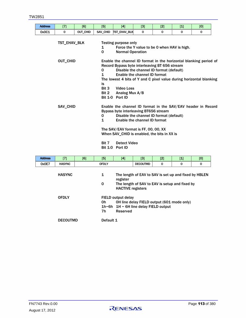
TW2851
FN7743 Rev.0.00 Page 113 of 380
August 17, 2012
Address [7] [6] [5] [4] [3] [2] [1] [0]
0x0C1 0 OUT_CHID SAV_CHID TST_EHAV_BLK 0 0 0 0
TST_EHAV_BLK Testing purpose only
1 Force the Y value to be 0 when HAV is high.
0 Normal Operation
OUT_CHID Enable the channel ID format in the horizontal blanking period of
Record Bypass byte interleaving BT 656 stream
0 Disable the channel ID format (default)
1 Enable the channel ID format
The lowest 4 bits of Y and C pixel value during horizontal blanking
is
Bit 3 Video Loss
Bit 2 Analog Mux A/B
Bit 1-0 Port ID
SAV_CHID Enable the channel ID format in the SAV/EAV header in Record
Bypass byte interleaving BT656 stream
0 Disable the channel ID format (default)
1 Enable the channel ID format
The SAV/EAV format is FF, 00, 00, XX
When SAV_CHID is enabled, the bits in XX is
Bit 7 Detect Video
Bit 1:0 Port ID
Address [7] [6] [5] [4] [3] [2] [1] [0]
0x0E7 HASYNC OFDLY DECOUTMD 0 0 0
HASYNC 1 The length of EAV to SAV is set up and fixed by HBLEN
register
0 The length of SAV to EAV is setup and fixed by
HACTIVE registers
OFDLY FIELD output delay
0h 0H line delay FIELD output (601 mode only)
1h~6h 1H ~ 6H line delay FIELD output
7h Reserved
DECOUTMD Default 1

TW2851
FN7743 Rev.0.00 Page 114 of 380
August 17, 2012
Address [7] [6] [5] [4] [3] [2] [1] [0]
0x0E8 HBLEN
HBLEN These bits are effective when HASYNC bit is set to 1. These bits
setup the length of EAV to SAV code when HASYNC bit is 1. Normal
value is (Total pixel per line – HACTIVE) value.
NTSC/PAL-M(60Hz) 8Ah = 858 – 720
PAL/SECAM(50Hz) 90h = 864 – 720
If register 0x00E[3] (ATREG for CH1) is set to 0, this value changes
into 8Ah or 90h at audio video format detection initial time
automatically according to CH1 video detection status.
Address [7] [6] [5] [4] [3] [2] [1] [0]
0x0E9 CKLM YDLY 0 0 0 0
CKLM Color Killer mode.
0 Normal (Default)
1 Fast (For special application)
TDLY Luma delay fine adjustment. This 2's complement number
provides –4 to +3 unit delay control (Default 3h)
Address [7] [6] [5] [4] [3] [2] [1] [0]
0x0EA 0 0 ADECRST 0 VDEC4RST VDEC3RST VDEC2RST VDEC1RST
ADECRST A 1 written to this bit resets the audio portion to its default state
but all register content remains unchanged. This bit is self-cleared.
VDECnRST A 1 written to this bit resets the VINn path Video Decoder portion to
its default state but all register content remain unchanged. This bit
is self cleared.
Address [7] [6] [5] [4] [3] [2] [1] [0]
0x0EB MISSCNT HSWIN
MISSCNT These bits set the threshold for horizontal sync miss count
threshold (Default 4h)
HSWIN These bits determine the VCR mode detection threshold (Default
4h)
Address [7] [6] [5] [4] [3] [2] [1] [0]
0x0EC PCLAMP
PCLAMP These bits set the clamping position from the PLL sync edge
(Default 2Ah)

TW2851
FN7743 Rev.0.00 Page 115 of 380
August 17, 2012
Address [7] [6] [5] [4] [3] [2] [1] [0]
0x0ED VLCKI VLCKO VMODE DETV AFLD VINT
VLCKI Vertical lock in time
0 Fastest (Default)
:
3 Slowest.
VLCKO Vertical lock out time
0 Fastest (Default)
:
3 Slowest
VMODE This bit controls the vertical detection window
1 Search mode
0 Vertical countdown mode (Default)
DETV 1 Recommended for special application only
0 Normal Vsync logic (Default)
AFLD Auto field generation control
0 Off (Default)
1 On
VINT Vertical integration time control
1 Short
0 Normal (Default)
Address [7] [6] [5] [4] [3] [2] [1] [0]
0x0EE BSHT VSHT
BSHT Burst PLL center frequency control (Default 0h)
VSHT Vsync output delay control in the increment of half line length
(Default 0h)

TW2851
FN7743 Rev.0.00 Page 116 of 380
August 17, 2012
Address [7] [6] [5] [4] [3] [2] [1] [0]
0x0EF CKILLMAX CKILLMIN
CKILLMAX These bits control the amount of color killer hysteresis. The
hysteresis amount is proportional to the value (Default 1h)
CKILLMIN These bits control the color killer threshold. Larger value gives
lower killer level (Default 28h)
Address [7] [6] [5] [4] [3] [2] [1] [0]
0x0F0 COMBMD HTL VTL
COMBMD 0 Adaptive mode (Default)
1 Fixed comb
HTL Adaptive Comb filter threshold control 1 (Default 4h)
VTL Adaptive Comb filter threshold control 2 (Default Ch)
Address [7] [6] [5] [4] [3] [2] [1] [0]
0x0F1 HPLC EVCNT PALC SDET 0 BYPASS 0 0
HPLC Reserved for internal use (Default 0)
EVCNT 1 Even field counter in special mode
0 Normal operation (Default)
PALC Reserved for future use (Default 0)
SDET ID detection sensitivity. A '1' is recommended (Default 1)
BYPASS It controls the standard detection and should be set to ‘1’ in
normal use (Default 1)

TW2851
FN7743 Rev.0.00 Page 117 of 380
August 17, 2012
Address [7] [6] [5] [4] [3] [2] [1] [0]
0x0F2 HPM ACCT SPM CBW
HPM Horizontal PLL acquisition time.
0 Normal
1 Auto2
2 Auto1 (Default)
3 Fast
ACCT ACC time constant
0 No ACC
1 Slow
2 Medium (Default)
3 Fast
SPM Burst PLL control
0 Slowest
1 Slow (Default)
2 Fast
3 Fastest
CBW Chroma low pass filter bandwidth control. Refer to filter curves
(Default 1)
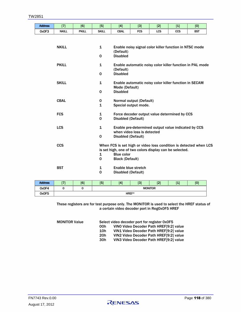
TW2851
FN7743 Rev.0.00 Page 118 of 380
August 17, 2012
Address [7] [6] [5] [4] [3] [2] [1] [0]
0x0F3 NKILL PKILL SKILL CBAL FCS LCS CCS BST
NKILL 1 Enable noisy signal color killer function in NTSC mode
(Default)
0 Disabled
PKILL 1 Enable automatic noisy color killer function in PAL mode
(Default)
0 Disabled
SKILL 1 Enable automatic noisy color killer function in SECAM
Mode (Default)
0 Disabled
CBAL 0 Normal output (Default)
1 Special output mode.
FCS 1 Force decoder output value determined by CCS
0 Disabled (Default)
LCS 1 Enable pre-determined output value indicated by CCS
when video loss is detected
0 Disabled (Default)
CCS When FCS is set high or video loss condition is detected when LCS
is set high, one of two colors display can be selected.
1 Blue color
0 Black (Default)
BST 1 Enable blue stretch
0 Disabled (Default)
Address [7] [6] [5] [4] [3] [2] [1] [0]
0x0F4 0 0 MONITOR
0x0F5 HREF*
These registers are for test purpose only. The MONITOR is used to select the HREF status of
a certain video decoder port in Reg0x0F5 HREF
MONITOR Value Select video decoder port for register 0x0F5
00h VIN0 Video Decoder Path HREF[9:2] value
10h VIN1 Video Decoder Path HREF[9:2] value
20h VIN2 Video Decoder Path HREF[9:2] value
30h VIN3 Video Decoder Path HREF[9:2] value

TW2851
FN7743 Rev.0.00 Page 119 of 380
August 17, 2012
Address [7] [6] [5] [4] [3] [2] [1] [0]
0x0F6 0 CVSTD1* CVFMT1
0x0F7 0 CVSTD2* CVFMT2
0x0F8 0 CVSTD3* CVFMT3
0x0F9 0 CVSTD4* CVFMT4
CVSTDn
CVFMTn
Address [7] [6] [5] [4] [3] [2] [1] [0]
0x0FA IDX1 NSEN1/SSEN1/PSEN1/WKTH1
0x0FB IDX2 NSEN2/SSEN2/PSEN2/WKTH2
0x0FC IDX3 NSEN3/SSEN3/PSEN3/WKTH3
0x0FD IDX4 NSEN4/SSEN4/PSEN4/WKTH4
NSENn/SSENn/PSENn/WKTHn shared the same 6 bits in the register. IDXn is used to
select which of the four parameters is being controlled. The write
sequence is a two steps process unless the same register is
written. A write of {ID,000000} selects one of the four registers to
be written. A subsequent write will actually write into the register.
(Default 0h)
IDXn 0 Controls the NTSC color carrier detection sensitivity
(NSENn) (Default 1Ah)
1 Controls the SECAM ID detection sensitivity (SSENn)
(Default 20h)
2 Controls the PAL ID detection sensitivity (PSENn)
(Default 1Ch)
3 Controls the weak signal detection sensitivity (WKTHn)
(Default 2Ah)
Address [7] [6] [5] [4] [3] [2] [1] [0]
0x0FE DEV_ID * REV_ID *
* Read only
DEV_ID The TW2851 product ID code is 01000
REV_ID The revision number is 0h

TW2851
FN7743 Rev.0.00 Page 120 of 380
August 17, 2012
Address [7] [6] [5] [4] [3] [2] [1] [0]
0x340 VDLOSS_TH1 VDLOSS_TH0
0x341 VDLOSS_TH3 VDLOSS_TH2
VDLOSS_THn Adjust the video loss signal presented to the backend modules
from video decoder 0, 1, 2, and 3.
0 The backend video loss signal is the same as the video
decoder video loss signal.
1 – 14 The backend video loss signal is asserted only when video
decoder video loss signal is asserted for more than
VDLOSS_THx fields.
15 The backend video loss signal is never asserted regardless
of the Video decoder video loss signal.
INTERNAL PATTERN GENERATOR
Address [7] [6] [5] [4] [3] [2] [1] [0]
0x303 0 1 PTRN_LIM_656 PTRN_SMALL PTRN_CHIP_ID PTRN_PAL PTRN_EN
PTRN_LIM_656 Limit the pixel value generated by the internal pattern generator
after the video decoder.
1 Limit Y to 235 maximum, 16 minimum
0 Do not limit
PTRN_SMALL Internal pattern generator generates small frame. For simulation
only
PTRN_CHIP_ID Specify the chip ID of this chip
PTRN_PAL 1 Internal pattern generator generates PAL pattern
0 Internal pattern generator generates NTSC pattern
PTRN_EN Enable Internal pattern generator to replace the video stream
from video decoder
1 Enable the pattern generator
0 Use the video decoder input
Address [7] [6] [5] [4] [3] [2] [1] [0]
0x304 0 0 0 0 PTRN_VIDEO_LOSS
PTRN_VIDEO_LOSS Generate the video loss signal from the internal pattern
generator
1 Video Loss
0 Video detected

TW2851
FN7743 Rev.0.00 Page 121 of 380
August 17, 2012
NOISE REDUCTION
Address [7] [6] [5] [4] [3] [2] [1] [0]
0x305 0 BP_NR_2S BP_NR_2Y BP_NR_2X 0 BP_NR_1S BP_NR_1Y BP_NR_1X
0x306 0 BP_NR_4S BP_NR_4Y BP_NR_4X 0 BP_NR_3S BP_NR_3Y BP_NR_3X
BP_NR_nX Bypass the noise reduction of display path for port n
1 Bypass
0 Do not bypass
BP_NR_nY Bypass the noise reduction of record path for port n
1 Bypass
0 Do not bypass
BP_NR_nS Bypass the noise reduction of SPOT path for port n
1 Bypass
0 Do not bypass
Address [7] [6] [5] [4] [3] [2] [1] [0]
0x350 NR2_SML_THD NR2_FR2 NR2_FR1 NR2_FR0 NR1_SML_THD NR1_FR2 NR1_FR1 NR1_FR0
0x351 NR4_SML_THD NR4_FR2 NR4_FR1 NR4_FR0 NR3_SML_THD NR3_FR2 NR3_FR1 NR3_FR0
NRn_FR0 Force port n noise reduction to level 0 – Disable noise reduction
NRn_FR1 Force port n noise reduction to level 1 – weak
NRn_FR2 Force port n noise reduction to level 2 – strong
NRn_SML_THD Default 0
Address [7] [6] [5] [4] [3] [2] [1] [0]
0x352 0 0 0 0 NR4_RST_DET NR3_RST_DET NR2_RST_DET NR1_RST_DET
NRn_RST_DET Reset the noise reduction detection for port n
Address [7] [6] [5] [4] [3] [2] [1] [0]
0x356 NR_DET_OUT_THD NR_DET_REF_VAR
NR_DET_OUT_THD Default 6
NR_DET_REF_VAR Default 1

TW2851
FN7743 Rev.0.00 Page 122 of 380
August 17, 2012
Address [7] [6] [5] [4] [3] [2] [1] [0]
0x357 NR_DET_NOISE_1L
0x358 NR_DET_NOISE_1H
0x359 NR_DET_NOISE_2L
0x35A NR_DET_NOISE_2H
0x35B NR_DET_NOISE_CL
0x35C NR_DET_NOISE_CH
0x35D NR_DET_SKIP_L
0x35E NR_DET_SKIP_H
NR_DET_NOISE_1L Lower bound of pixel distance for noise level 1
Default: 3
NR_DET_NOISE_1H Higher bound of pixel distance for noise level 1
Default: 10
NR_DET_NOISE_2L Lower bound of pixel distance for noise level 2
Default: 5
NR_DET_NOISE_2H Higher bound of pixel distance for noise level 2
Default: 15
NR_DET_NOISE_CL Lower bound of pixel distance for chroma noise level
Default: 4
NR_DET_NOISE_CH Higher bound of pixel distance for chroma noise level
Default: 10
NR_DET_SKIP_L Pixels with value below this threshold will not be processed
Default: 25
NR_DET_SKIP_H Pixels with value above this threshold will not be processed
Default: 240
Address [7] [6] [5] [4] [3] [2] [1] [0]
0x35F NRDET4_LVL* NRDET3_LVL* NRDET2_LVL* NRDET1_LVL*
*Read only
NRDETn_LVL Detected noise level for channel n
0 Disable noise
1 Weak noise reduction
2 Strong noise reduction

TW2851
FN7743 Rev.0.00 Page 123 of 380
August 17, 2012
DOWNSCALER
Address [7] [6] [5] [4] [3] [2] [1] [0]
0x301 0 BP_SCL_2S BP_SCL_2Y BP_SCL_2X 0 BP_SCL_1S BP_SCL_1Y BP_SCL_1X
0x302 0 BP_SCL_4S BP_SCL_4Y BP_SCL_4X 0 BP_SCL_3S BP_SCL_3Y BP_SCL_3X
BP_SCL_nX Bypass the down scaler of display path for port n
1 Bypass
0 Do not bypass
BP_SCL_nY Bypass the down scaler of record path for port n
1 Bypass
0 Do not bypass
BP_SCL_nS Bypass the down scaler of SPOT path for port n
1 Bypass
0 Do not bypass
Address [7] [6] [5] [4] [3] [2] [1] [0]
0x380 HSCL_DISP_TARG_1
0x390 HSCL_DISP_TARG_2
0x3A0 HSCL_DISP_TARG_3
0x3B0 HSCL_DISP_TARG_4
HSCL_DISP_TARG_n The display down scaler target horizontal size for port n. The unit
is in multiple of 16 pixels
Address [7] [6] [5] [4] [3] [2] [1] [0]
0x381 VSCL_DISP_TARG_1
0x391 VSCL_DISP_TARG_2
0x3A1 VSCL_DISP_TARG_3
0x3B1 VSCL_DISP_TARG_4
VSCL_DISP_TARG_n The display down scaler target vertical size for port n. The unit is in
multiple of 8 lines
Address [7] [6] [5] [4] [3] [2] [1] [0]
0x382 HSCL_REC_TARG_1
0x392 HSCL_REC_TARG_2
0x3A2 HSCL_REC_TARG_3
0x3B2 HSCL_REC_TARG_4
HSCL_REC_TARG_n The record down scaler target horizontal size for port n. The unit
is in multiple of 16 pixels

TW2851
FN7743 Rev.0.00 Page 124 of 380
August 17, 2012
Address [7] [6] [5] [4] [3] [2] [1] [0]
0x383 VSCL_REC_TARG_1
0x393 VSCL_REC_TARG_2
0x3A3 VSCL_REC_TARG_3
0x3B3 VSCL_REC_TARG_4
VSCL_REC_TARG_n The record down scaler target vertical size for port n. The unit is in
multiple of 8 lines
Address [7] [6] [5] [4] [3] [2] [1] [0]
0x384 HSCL_SPOT_TARG_1
0x394 HSCL_ SPOT _TARG_2
0x3A4 HSCL_ SPOT _TARG_3
0x3B4 HSCL_ SPOT _TARG_4
HSCL_SPOT_TARG_n The SPOT down scaler target horizontal size for port n. The unit
is in multiple of 16 pixels
Address [7] [6] [5] [4] [3] [2] [1] [0]
0x385 VSCL_ SPOT _TARG_1
0x395 VSCL_ SPOT _TARG_2
0x3A5 VSCL_ SPOT _TARG_3
0x3B5 VSCL_ SPOT _TARG_4
VSCL_SPOT_TARG_n The SPOT down scaler target vertical size for port n. The unit is in
multiple of 8 lines
Address [7] [6] [5] [4] [3] [2] [1] [0]
0x387 HSCL_DISP_SRC_1
0x397 HSCL_DISP_ SRC _2
0x3A7 HSCL_DISP_ SRC _3
0x3B7 HSCL_DISP_ SRC _4
HSCL_DISP_SRC_n The display down scaler source horizontal size for port n. The unit is
in multiple of 16 pixels
Address [7] [6] [5] [4] [3] [2] [1] [0]
0x388 VSCL_DISP_SRC_1
0x398 VSCL_DISP_ SRC _2
0x3A8 VSCL_DISP_ SRC _3
0x3B8 VSCL_DISP_ SRC _4
VSCL_DISP_SRC_n The display down scaler source vertical size for port n. The unit is in
multiple of 8 lines

TW2851
FN7743 Rev.0.00 Page 125 of 380
August 17, 2012
Address [7] [6] [5] [4] [3] [2] [1] [0]
0x389 HSCL_REC_ SRC _1
0x399 HSCL_REC_ SRC _2
0x3A9 HSCL_REC_ SRC _3
0x3B9 HSCL_REC_ SRC _4
HSCL_REC_SRC_n The record down scaler source horizontal size for port n. The unit is
in multiple of 16 pixels
Address [7] [6] [5] [4] [3] [2] [1] [0]
0x38A VSCL_REC_ SRC _1
0x39A VSCL_REC_ SRC _2
0x3AA VSCL_REC_ SRC _3
0x3BA VSCL_REC_ SRC _4
VSCL_REC_SRC_n The record down scaler source vertical size for port n. The unit is in
multiple of 8 lines
Address [7] [6] [5] [4] [3] [2] [1] [0]
0x38B HSCL_SPOT_ SRC _1
0x39B HSCL_ SPOT _ SRC _2
0x3AB HSCL_ SPOT _ SRC _3
0x3BB HSCL_ SPOT _ SRC _4
HSCL_SPOT_SRC_n The SPOT down scaler source horizontal size for port n. The unit is
in multiple of 16 pixels
Address [7] [6] [5] [4] [3] [2] [1] [0]
0x38C VSCL_ SPOT _ SRC _1
0x39C VSCL_ SPOT _ SRC _2
0x3AC VSCL_ SPOT _ SRC _3
0x3BC VSCL_ SPOT _ SRC _4
VSCL_SPOT_SRC_n The SPOT down scaler source vertical size for port n. The unit is in
multiple of 8 lines
Address [7] [6] [5] [4] [3] [2] [1] [0]
0x386 FLDPOL_1S FLDPOL_1Y FLDPOL_1X
0x396 FLDPOL_2S FLDPOL_2Y FLDPOL_2X
0x3A6 FLDPOL_3S FLDPOL_3Y FLDPOL_3X
0x3B6 FLDPOL_4S FLDPOL_4Y FLDPOL_4X
FLDPOL_nX The display downscaler field polarity control for port n
FLDPOL_nY The record downscaler field polarity control for port n
FLDPOL_nS The SPOT downscaler field polarity control for port n
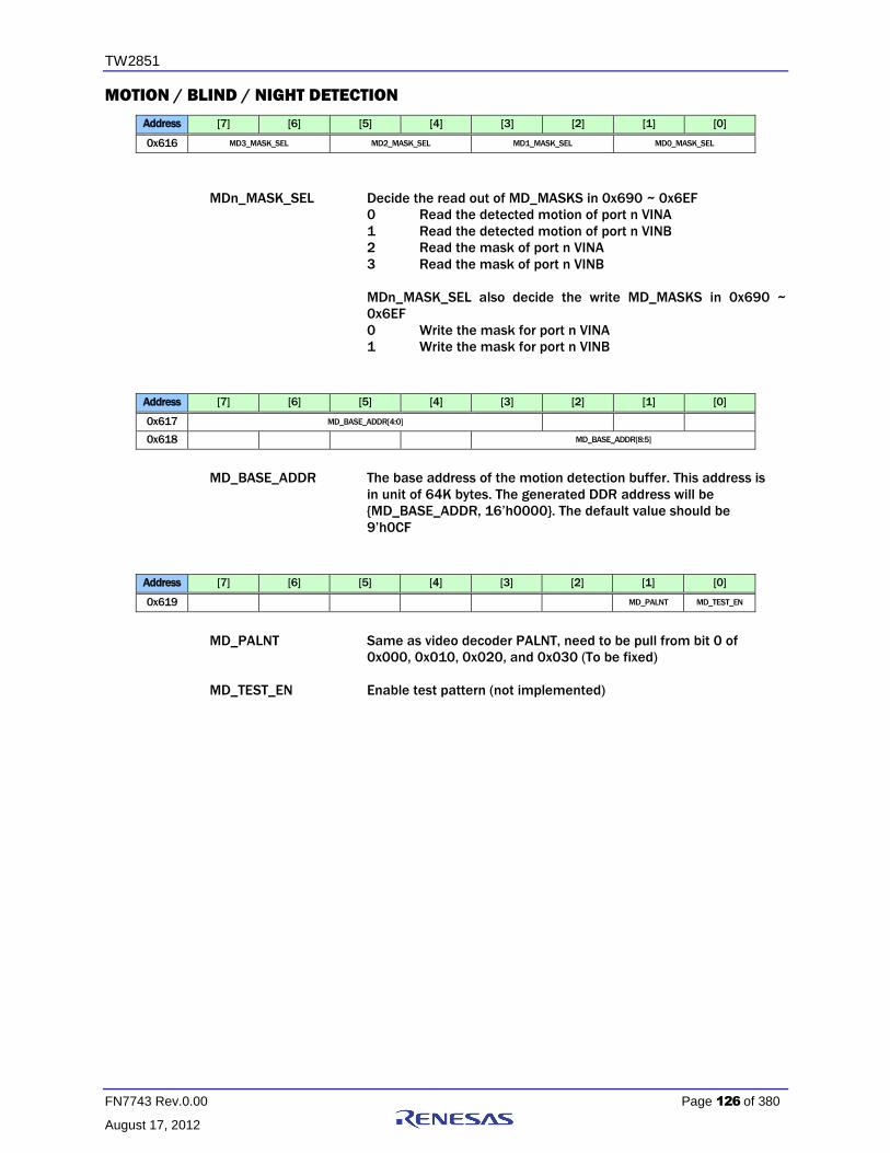
TW2851
FN7743 Rev.0.00 Page 126 of 380
August 17, 2012
MOTION / BLIND / NIGHT DETECTION
Address [7] [6] [5] [4] [3] [2] [1] [0]
0x616 MD3_MASK_SEL MD2_MASK_SEL MD1_MASK_SEL MD0_MASK_SEL
MDn_MASK_SEL Decide the read out of MD_MASKS in 0x690 ~ 0x6EF
0 Read the detected motion of port n VINA
1 Read the detected motion of port n VINB
2 Read the mask of port n VINA
3 Read the mask of port n VINB
MDn_MASK_SEL also decide the write MD_MASKS in 0x690 ~
0x6EF
0 Write the mask for port n VINA
1 Write the mask for port n VINB
Address [7] [6] [5] [4] [3] [2] [1] [0]
0x617 MD_BASE_ADDR[4:0]
0x618 MD_BASE_ADDR[8:5]
MD_BASE_ADDR The base address of the motion detection buffer. This address is
in unit of 64K bytes. The generated DDR address will be
{MD_BASE_ADDR, 16’h0000}. The default value should be
9’h0CF
Address [7] [6] [5] [4] [3] [2] [1] [0]
0x619 MD_PALNT MD_TEST_EN
MD_PALNT Same as video decoder PALNT, need to be pull from bit 0 of
0x000, 0x010, 0x020, and 0x030 (To be fixed)
MD_TEST_EN Enable test pattern (not implemented)

TW2851
FN7743 Rev.0.00 Page 127 of 380
August 17, 2012
Address [7] [6] [5] [4] [3] [2] [1] [0]
0x61A MD_DIS MD_DUAL_EN MD_STRB MD_STRB_EN BD_CELLSENS
0x61B MD_TMPSENS MD_PIXEL_OS
0x61C MD_REFFLD MD_FIELD MD_LVSENS
0x61D MD_CELSENS MD_SPEED
0x61E MD_SPSENS BD_LVSENS
0x61F ND_TMPSENS ND_LVSENS
Register 0x61A ~ 0x61F are used to control the motion detection of 8 inputs (A / B inputs
of 4 video decoders). In order to select the specific input to control, set the corresponding
bit of MDCH_SEL in 0x676.
MD_DIS Disable the motion and blind detection.
0 Enable motion and blind detection (default)
1 Disable motion and blind detection
MD_DUAL_EN Enable pseudo 8 channel for motion detection
MD_STRB Request to start motion detection on manual trigger mode
0 None Operation (default)
1 Request to start motion detection
MD_STRB_EN Select the trigger mode of motion detection
0 Automatic trigger mode of motion detection (default)
1 Manual trigger mode for motion detection
BD_CELSENS Define the threshold of cell for blind detection.
0 Low threshold (More sensitive) (default)
: :
3 High threshold (Less sensitive)
MD_TMPSENS Control the temporal sensitivity of motion detector.
0 More Sensitive (default)
: :
15 Less Sensitive
MD_PIXEL_OS Adjust the horizontal starting position for motion detection
0 0 pixel (default)
: :
15 15 pixels
MD_REFFLD Control the updating time of reference field for motion detection.
0 Update reference field every field (default)
1 Update reference field according to MD_SPEED
MD_FIELD Select the field for motion detection.
0 Detecting motion for only odd field (default)
1 Detecting motion for only even field
2 Detecting motion for any field
3 Detecting motion for both odd and even field
MD_LVSENS Control the level sensitivity of motion detector.
0 More sensitive (default)
: :
31 Less sensitive
MD_CELSENS Define the threshold of sub-cell number for motion detection.

TW2851
FN7743 Rev.0.00 Page 128 of 380
August 17, 2012
0 Motion is detected if 1 sub-cell has motion (More sensitive)
(default)
1 Motion is detected if 2 sub-cells have motion
2 Motion is detected if 3 sub-cells have motion
3 Motion is detected if 4 sub-cells have motion (Less
sensitive)
MD_SPEED Control the velocity of motion detector.
Large value is suitable for slow motion detection.
In MD_DUAL_EN = 1, MD_SPEED should be limited to 0 ~ 31.
0 1 field intervals (default)
1 2 field intervals
: :
61 62 field intervals
62 63 field intervals
63 Not supported
MD_SPSENS Control the spatial sensitivity of motion detector.
0 More Sensitive (default)
: :
15 Less Sensitive
BD_LVSENS Define the threshold of level for blind detection.
0 Low threshold (More sensitive) (default)
: :
15 High threshold (Less sensitive)
ND_TMPSENS Define the threshold of temporal sensitivity for night detection.
0 Low threshold (More sensitive) (default)
: :
15 High threshold (Less sensitive)
ND_LVSENS Define the threshold of level for night detection.
0 Low threshold (More sensitive) (default)
: :
15 High threshold (Less sensitive)
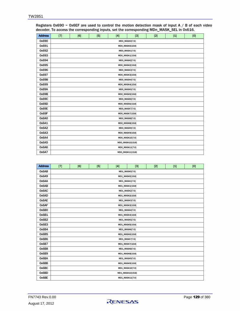
TW2851
FN7743 Rev.0.00 Page 129 of 380
August 17, 2012
Registers 0x690 ~ 0x6EF are used to control the motion detection mask of input A / B of each video
decoder. To access the corresponding inputs, set the corresponding MDn_MASK_SEL in 0x616.
Address [7] [6] [5] [4] [3] [2] [1] [0]
0x690 MD0_MASK0[7:0]
0x691 MD0_MASK0[15:8]
0x692 MD0_MASK1[7:0]
0x693 MD0_MASK1[15:8]
0x694 MD0_MASK2[7:0]
0x695 MD0_MASK2[15:8]
0x696 MD0_MASK3[7:0]
0x697 MD0_MASK3[15:8]
0x698 MD0_MASK4[7:0]
0x699 MD0_MASK4[15:8]
0x69A MD0_MASK5[7:0]
0x69B MD0_MASK5[15:8]
0x69C MD0_MASK6[7:0]
0x69D MD0_MASK6[15:8]
0x69E MD0_MASK7[7:0]
0x69F MD0_MASK7[15:8]
0x6A0 MD0_MASK8[7:0]
0x6A1 MD0_MASK8[15:8]
0x6A2 MD0_MASK9[7:0]
0x6A3 MD0_MASK9[15:8]
0x6A4 MD0_MASK10[7:0]
0x6A5 MD0_MASK10[15:8]
0x6A6 MD0_MASK11[7:0]
0x6A7 MD0_MASK11[15:8]
Address [7] [6] [5] [4] [3] [2] [1] [0]
0x6A8 MD1_MASK0[7:0]
0x6A9 MD1_MASK0[15:8]
0x6AA MD1_MASK1[7:0]
0x6AB MD1_MASK1[15:8]
0x6AC MD1_MASK2[7:0]
0x6AD MD1_MASK2[15:8]
0x6AE MD1_MASK3[7:0]
0x6AF MD1_MASK3[15:8]
0x6B0 MD1_MASK4[7:0]
0x6B1 MD1_MASK4[15:8]
0x6B2 MD1_MASK5[7:0]
0x6B3 MD1_MASK5[15:8]
0x6B4 MD1_MASK6[7:0]
0x6B5 MD1_MASK6[15:8]
0x6B6 MD1_MASK7[7:0]
0x6B7 MD1_MASK7[15:8]
0x6B8 MD1_MASK8[7:0]
0x6B9 MD1_MASK8[15:8]
0x6BA MD1_MASK9[7:0]
0x6BB MD1_MASK9[15:8]
0x6BC MD1_MASK10[7:0]
0x6BD MD1_MASK10[15:8]
0x6BE MD1_MASK11[7:0]

TW2851
FN7743 Rev.0.00 Page 130 of 380
August 17, 2012
Address [7] [6] [5] [4] [3] [2] [1] [0]
0x6BF MD1_MASK11[15:8]
Address [7] [6] [5] [4] [3] [2] [1] [0]
0x6C0 MD2_MASK0[7:0]
0x6C1 MD2_MASK0[15:8]
0x6C2 MD2_MASK1[7:0]
0x6C3 MD2_MASK1[15:8]
0x6C4 MD2_MASK2[7:0]
0x6C5 MD2_MASK2[15:8]
0x6C6 MD2_MASK3[7:0]
0x6C7 MD2_MASK3[15:8]
0x6C8 MD2_MASK4[7:0]
0x6C9 MD2_MASK4[15:8]
0x6CA MD2_MASK5[7:0]
0x6CB MD2_MASK5[15:8]
0x6CC MD2_MASK6[7:0]
0x6CD MD2_MASK6[15:8]
0x6CE MD2_MASK7[7:0]
0x6CF MD2_MASK7[15:8]
0x6D0 MD2_MASK8[7:0]
0x6D1 MD2_MASK8[15:8]
0x6D2 MD2_MASK9[7:0]
0x6D3 MD2_MASK9[15:8]
0x6D4 MD2_MASK10[7:0]
0x6D5 MD2_MASK10[15:8]
0x6D6 MD2_MASK11[7:0]
0x6D7 MD2_MASK11[15:8]
Address [7] [6] [5] [4] [3] [2] [1] [0]
0x6D8 MD3_MASK0[7:0]
0x6D9 MD3_MASK0[15:8]
0x6DA MD3_MASK1[7:0]
0x6DB MD3_MASK1[15:8]
0x6DC MD3_MASK2[7:0]
0x6DD MD3_MASK2[15:8]
0x6DE MD3_MASK3[7:0]
0x6DF MD3_MASK3[15:8]
0x6E0 MD3_MASK4[7:0]
0x6E1 MD3_MASK4[15:8]
0x6E2 MD3_MASK5[7:0]
0x6E3 MD3_MASK5[15:8]
0x6E4 MD3_MASK6[7:0]
0x6E5 MD3_MASK6[15:8]
0x6E6 MD3_MASK7[7:0]
0x6E7 MD3_MASK7[15:8]
0x6E8 MD3_MASK8[7:0]
0x6E9 MD3_MASK8[15:8]
0x6EA MD3_MASK9[7:0]
0x6EB MD3_MASK9[15:8]
0x6EC MD3_MASK10[7:0]

TW2851
FN7743 Rev.0.00 Page 131 of 380
August 17, 2012
Address [7] [6] [5] [4] [3] [2] [1] [0]
0x6ED MD3_MASK10[15:8]
0x6EE MD3_MASK11[7:0]
0x6EF MD3_MASK11[15:8]
MDx_MASK Define the motion Mask/Detection cell for VIN x. MD_MASK[15] is
right end and
MD_MASK[0] is left end of column.
In writing mode
0 Non-masking cell for motion detection (default)
1 Masking cell for motion detection
In reading mode when MDn_MASK_SEL = “0”
0 Motion is not detected for cell
1 Motion is detected for cell
In reading mode when MDn_MASK_SEL = “1”
0 Non-masked cell
1 Masked cell
Address [7] [6] [5] [4] [3] [2] [1] [0]
0x6F0 MD_STRB_DET*
*Read only bit
MD_STRBn 1 MD strobe has been performed at channel n
0 MD strobe has not yet been performed at channel n
Address [7] [6] [5] [4] [3] [2] [1] [0]
0x6F1 NOVID_DET_0B* MD_DET_0B* BD_DET_0B* ND_DET_0B* NOVID_DET_0A* MD_DET_0A* BD_DET_0A* ND_DET_0A*
0x6F2 NOVID_DET_1B* MD_DET_1B* BD_DET_1B* ND_DET_1B* NOVID_DET_1A* MD_DET_1A* BD_DET_1A* ND_DET_1A*
0x6F3 NOVID_DET_2B* MD_DET_2B* BD_DET_2B* ND_DET_2B* NOVID_DET_2A* MD_DET_2A* BD_DET_2A* ND_DET_2A*
0x6F4 NOVID_DET_3B* MD_DET_3B* BD_DET_3B* ND_DET_3B* NOVID_DET_3A* MD_DET_3A* BD_DET_3A* ND_DET_3A*
*Read only bits
NOVID_DET_mA NO_VIDEO Detected from port m, analog path A (read only)
NOVID_DET_mB NO_VIDEO Detected from port m, analog path B (read only)
MD_DET_mA Motion Detected from port m, analog path A (read only)
MD_DET_mB Motion Detected from port m, analog path B (read only)
BD_DET_mA Blind Detected from port m, analog path A (read only)
BD_DET_mB Blind Detected from port m, analog path B (read only)
ND_DET_mA Night Detected from port m, analog path A (read only)
ND_DET_mB Night Detected from port m, analog path B
Digital Input Interface
656 / 601 / RGB PORT
Address [7] [6] [5] [4] [3] [2] [1] [0]

TW2851
FN7743 Rev.0.00 Page 132 of 380
August 17, 2012
0x100 0 0 LIM_PB
_656
656_PB_EC
_BYPASS PB_CH_NO_VIDEO*
* Read only
LIM_PB_656 Specify the Clamping mode for PB input data at BT 656 mode
1 maximum 235, minimum 16
0 maximum 254, minimum 1
656_PB_EC_BYPASS Bypass the error correction of BT 656
1 Bypass error correction
0 Do not bypass error correction when the parity check is
wrong
PB_CH_NO_VIDEO[n] NO_VIDEO Status of Playback channel n (Read Only)
Address [7] [6] [5] [4] [3] [2] [1] [0]
0x101 PB_PORT_SEL3* PB_PORT_SEL2* PB_PORT_SEL1* PB_PORT_SEL0*
* Read only
PB_PORT_SELn The playback channel n mux selection of the physical playback
input port number (read only)
0 Channel n has input from Playback port 0
1 Channel n has input from Playback port 1
2 Channel n has input from Playback port 2
3 Channel n has input from Playback port 3
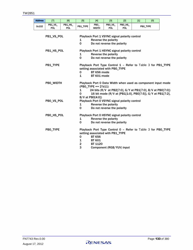
TW2851
FN7743 Rev.0.00 Page 133 of 380
August 17, 2012
Address [7] [6] [5] [4] [3] [2] [1] [0]
0x102 PB1_VS_
POL
PB1_HS_
POL PB1_TYPE
PB0_
WIDTH
PB0_VS_
POL
PB0_HS_
POL PB0_TYPE
PB1_VS_POL Playback Port 1 VSYNC signal polarity control
1 Reverse the polarity
0 Do not reverse the polarity
PB1_HS_POL Playback Port 1 HSYNC signal polarity control
1 Reverse the polarity
0 Do not reverse the polarity
PB1_TYPE Playback Port Type Control 1 – Refer to Table 3 for PB1_TYPE
setting associated with PB0_TYPE
0 BT 656 mode
1 BT 601 mode
PB0_WIDTH Playback Port 0 Data Width when used as component input mode
(PB0_TYPE == 2’b11)
1 24 bits (R/V at PB2[7:0], G/Y at PB1[7:0], B/V at PB0[7:0])
0 16 bit mode (R/V at {PB1[1:0], PB0[7:5]}, G/Y at PB1[7:2],
B/V at PB0[4:0])
PB0_VS_POL Playback Port 0 VSYNC signal polarity control
1 Reverse the polarity
0 Do not reverse the polarity
PB0_HS_POL Playback Port 0 HSYNC signal polarity control
1 Reverse the polarity
0 Do not reverse the polarity
PB0_TYPE Playback Port Type Control 0 – Refer to Table 3 for PB0_TYPE
setting associated with PB1_TYPE
0 BT 656
1 BT 601
2 BT 1120
3 Component (RGB/YUV) input
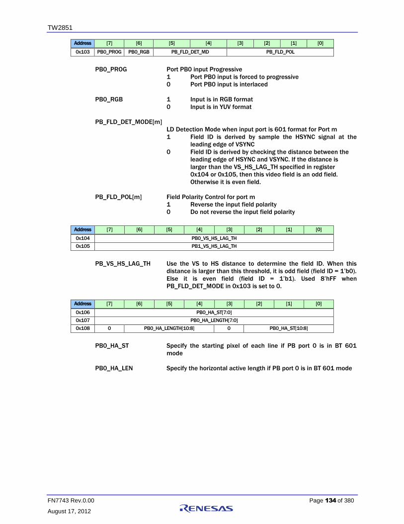
TW2851
FN7743 Rev.0.00 Page 134 of 380
August 17, 2012
Address [7] [6] [5] [4] [3] [2] [1] [0]
0x103 PB0_PROG PB0_RGB PB_FLD_DET_MD PB_FLD_POL
PB0_PROG Port PB0 input Progressive
1 Port PB0 input is forced to progressive
0 Port PB0 input is interlaced
PB0_RGB 1 Input is in RGB format
0 Input is in YUV format
PB_FLD_DET_MODE[m]
LD Detection Mode when input port is 601 format for Port m
1 Field ID is derived by sample the HSYNC signal at the
leading edge of VSYNC
0 Field ID is derived by checking the distance between the
leading edge of HSYNC and VSYNC. If the distance is
larger than the VS_HS_LAG_TH specified in register
0x104 or 0x105, then this video field is an odd field.
Otherwise it is even field.
PB_FLD_POL[m] Field Polarity Control for port m
1 Reverse the input field polarity
0 Do not reverse the input field polarity
Address [7] [6] [5] [4] [3] [2] [1] [0]
0x104 PB0_VS_HS_LAG_TH
0x105 PB1_VS_HS_LAG_TH
PB_VS_HS_LAG_TH Use the VS to HS distance to determine the field ID. When this
distance is larger than this threshold, it is odd field (field ID = 1’b0).
Else it is even field (field ID = 1’b1). Used 8’hFF when
PB_FLD_DET_MODE in 0x103 is set to 0.
Address [7] [6] [5] [4] [3] [2] [1] [0]
0x106 PB0_HA_ST[7:0]
0x107 PB0_HA_LENGTH[7:0]
0x108 0 PB0_HA_LENGTH[10:8] 0 PB0_HA_ST[10:8]
PB0_HA_ST Specify the starting pixel of each line if PB port 0 is in BT 601
mode
PB0_HA_LEN Specify the horizontal active length if PB port 0 is in BT 601 mode

TW2851
FN7743 Rev.0.00 Page 135 of 380
August 17, 2012
Address [7] [6] [5] [4] [3] [2] [1] [0]
0x109 PB0_VA1_ST[7:0]
0x10A PB0_VA2_ST[7:0]
0x10B PB0_VA_LEN[7:0]
0x10C 0 0 PB0_VA_LEN[9:8] PB0_VA2_ST[9:8] PB0_VA1_ST[9:8]
PB0_VAx_ST Specify the starting line if PB port 0 is in BT 601 mode
PB0_VA1_ST: The starting line of even field
PB0_VA2_ST: The starting line of odd field
PB0_VA_LEN Specify the vertical active length if PB port 0 is in BT 601 mode
Address [7] [6] [5] [4] [3] [2] [1] [0]
0x10D PB1_HA_ST[7:0]
0x10E PB1_HA_LEN[7:0]
0x10F 0 PB1_HA_LEN[10:8] 0 PB1_HA_ST[10:8]
PB1_HA_ST Specify the starting pixel of each line if PB port 1 is in BT 601
mode
PB1_HA_LEN Specify the horizontal active length if PB port 1 is in BT 601 mode
Address [7] [6] [5] [4] [3] [2] [1] [0]
0x110 PB1_VA1_ST[7:0]
0x111 PB1_VA2_ST[7:0]
0x112 PB1_VA_LEN[7:0]
0x113 0 0 PB1_VA_LEN[9:8] PB1_VA2_ST[9:8] PB1_VA1_ST[9:8]
PB1_VAx_ST Specify the starting line if PB port 1 is in BT 601 mode
PB1_VA1_ST: The starting line of even field
PB1_VA2_ST: The starting line of odd field
PB1_VA_LEN Specify the vertical active length if PB port1 is in BT 601 mode

TW2851
FN7743 Rev.0.00 Page 136 of 380
August 17, 2012
CHID DECODE / STROBE
Address [7] [6] [5] [4] [3] [2] [1] [0]
0x120 PB0_MAN_STRB_EN PB0_MAN_PIC_TYPE
0x130 PB1_MAN_STRB_EN PB1_MAN_PIC_TYPE
0x140 PB2_MAN_STRB_EN PB2_MAN_PIC_TYPE
0x150 PB3_MAN_STRB_EN PB3_MAN_PIC_TYPE
PBm_MAN_STRB_EN Enable manual strobe mode for PB port m
1 Enable
0 Disable
PBm_MAN_PIC_TYPE Specify the picture type used in manual strobe mode for PB port m
Address [7] [6] [5] [4] [3] [2] [1] [0]
0x121 PB0_MAN_CH1_ID PB0_MAN_CH0_ID
0x122 PB0_MAN_CH3_ID PB0_MAN_CH2_ID
0x131 PB1_MAN_CH1_ID PB1_MAN_CH0_ID
0x132 PB1_MAN_CH3_ID PB1_MAN_CH2_ID
0x141 PB2_MAN_CH1_ID PB2_MAN_CH0_ID
0x142 PB2_MAN_CH3_ID PB2_MAN_CH2_ID
0x151 PB3_MAN_CH1_ID PB3_MAN_CH0_ID
0x152 PB3_MAN_CH3_ID PB3_MAN_CH2_ID
PBm_MAN_CHn_ID Specify the channel ID to be used at PB port m channel n in
Manual Strobe mode
PBm_MAN_CHn_ID[3:2] chip ID
PBm_MAN_CHn_ID[1:0] channel ID

TW2851
FN7743 Rev.0.00 Page 137 of 380
August 17, 2012
Address [7] [6] [5] [4] [3] [2] [1] [0]
0x123 0 PB0_AUTO_STRB_EN PB0_FORCE_LIVE PB0_MAN_STRB_FLD PB0_MAN_ANA
0x133 0 PB1_AUTO_STRB_EN PB1_FORCE_LIVE PB1_MAN_STRB_FLD PB1_MAN_ANA
0x143 0 PB2_FORCE_LIVE PB2_MAN_STRB_FLD PB2_MAN_ANA
0x153 0 PB3_FORCE_LIVE PB3_MAN_STRB_FLD PB3_MAN_ANA
PBm_AUTO_STRB_EN
Enable playback port m automatic strobe using the channel ID
embedded in the VBI. Only PB0 and PB1 has channel ID decoder.
PB2 and PB3 do not support audio CHID.
1 Enable to use the channel ID embedded in the VBI to
strobe. In this mode, the Strobe signal is sent out
automatically without CPU issuing a strobe signal.
0 Disable: Use the channel ID specified by the register
0x120 ~ 0x122, 0x130 ~ 0x132, 0x140 ~0x142, 0x150 ~
0x152 to strobe.
PBm_FORCE_LIVE Force the playback to strobe on whatever input video stream.
1 When this bit is set to 1, the strobe is always sent out. It
will behave like a LIVE input. When this mode is on, the
PBm_MAN_PIC_TYPE has to be set to 0x01.
0 When this bit is set to 0, the strobe will be sent out only if
there is a match if PB_CHNUM with the channel ID from
the VBI, or the channel ID specified in the registers in
0x120 ~0x122, 0x130 ~ 0x132, 0x140 ~ 0x142, 0x150 ~
0x152.
Address [7] [6] [5] [4] [3] [2] [1] [0]
0x129 PB0_AUTO_STROBE_CH_EN PB0_VACTIVE[9:8] PB0_VDELAY[9:8]
0x139 PB1_AUTO_STROBE_CH_EN PB1_VACTIVE[9:8] PB1_VDELAY[9:8]
0x149 PB2_VACTIVE[9:8] PB2_VDELAY[9:8]
0x159 PB3_VACTIVE[9:8] PB3_VDELAY[9:8]
PBn_AUTO_STROBE_CH_EN[m]
Specify whether to turn on the auto strobe for port n, on channels
m. Only PB0 and PB1 have channel ID decoder. PB2 and PB3 do
not support audio CHID.

TW2851
FN7743 Rev.0.00 Page 138 of 380
August 17, 2012
Address [7] [6] [5] [4] [3] [2] [1] [0]
0x12A 0 PB0_CHID_FLD_OS PB0_DID_EN PB0_AID_EN PB0_FLT_EN PB0_RIC_EN PB0_AUTO_CHID_DET
0x13A 0 PB1_CHID_FLD_OS PB1_DID_EN PB1_AID_EN PB1_FLT_EN PB1_RIC_EN PB1_AUTO_CHID_DET
PBm_CHID_FLD_OS The PB port m CHID line offset of even field relative to odd field.
2 One line more than odd field
1 Same offset as odd field
0 One line less than odd field
PBm_DID_EN Enable digital channel ID detection for the PB port m
1 Turn on digital channel ID decoding
0 Turn off digital channel ID decoding
PBm_AID_EN Enable the Analog channel ID detection for PB port m
1 Turn on analog channel ID detection
0 Turn off analog channel ID detection
PBm_RIC_EN Select the run-in clock mode for analog channel ID
1 Run-in clock mode
0 No run-in clock mode
PBm_FLT_EN Select the LPF filter mode for playback input
0 Bypass mode
1 Enable the LPF filter
PBm_AUTO_CHID_DET Select the detection mode of Analog channel ID for playback input
port m
0 Manual detection mode for Analog channel ID
1 Automatic detection mode for Analog channel ID

TW2851
FN7743 Rev.0.00 Page 139 of 380
August 17, 2012
Address [7] [6] [5] [4] [3] [2] [1] [0]
0x12B PB0_CHID_LINE_SIZE PB0_CHID_V_OFST
0x13B PB1_CHID_LINE_SIZE PB1_CHID_V_OFST
PBm_CHID_LINE_SIZE Control the line width for Analog Channel ID for playback
input port m in manual detection mode (PBm_AUTO_CHID_DET =
0)
0 1 line
1 2 lines
:
7 8 lines (Default)
PBm_CHID_V_OFST Control the vertical starting offset from field transition for analog
channel ID
0 No offset
:
8 (default)
:
31
Address [7] [6] [5] [4] [3] [2] [1] [0]
0x12C PB0_CHID_H_OFST
0x13C PB1_CHID_H_OFST
PBm_CHID_H_OFST Define the horizontal starting offset of analog channel ID in
manual
detection mode (PBm_AUTO_CHID_DET = 0)
Address [7] [6] [5] [4] [3] [2] [1] [0]
0x12D 0 0 PB0_VAV_CHK PB0_ANA_CHID_BW
0x13D 0 0 PB1_VAV_CHK PB1_ANA_CHID_BW
PBm_VAV_CHK Enable the channel ID detection in vertical active period
0 Enable the channel ID detection for VBI period only
(default)
1 Enable the channel ID detection for VBI and active period
PBm_ANA_CHID_BW Define the pixel width for each bit of analog channel ID
0 1 pixel
:
31 32 pixels

TW2851
FN7743 Rev.0.00 Page 140 of 380
August 17, 2012
Address [7] [6] [5] [4] [3] [2] [1] [0]
0x12E PB0_CHID_MID_VAL
0x13E PB1_CHID_MID_VAL
PBm_CHID_MID_VAL Define the slicer threshold level to detect bit “0” or bit “1” from
analog channel ID (default 128)
Address [7] [6] [5] [4] [3] [2] [1] [0]
0x15F 0 0 0 0 0 0 PB_NOVID_MD
PB_NOVID_MD Select the No-Video flag generation mode
0 Faster
1 Fast
2 Slow
3 Slower (default)
Address [7] [6] [5] [4] [3] [2] [1] [0]
0x160 0 PB_STOP0 PB_HSCL_BYP0 PB_ANA0 PB_CHNUM0
0x170 0 PB_STOP1 PB_HSCL_BYP1 PB_ANA1 PB_CHNUM1
0x180 0 0 PB_HSCL_BYP2 PB_ANA2 PB_CHNUM2
0x190 0 0 PB_HSCL_BYP3 PB_ANA3 PB_CHNUM3
PB_STOPn Disable the auto strobe operation for playback channel n
0 Normal Operation (default)
1 Stop the auto strobe operation for playback channel n
PB_ HSCL_BYPn Bypass the horizontal scaler for playback channel n
0 Normal operation
1 Bypass the horizontal scaler
PB_ANAn The analog input selection of channel n
0 Select VINA
1 Select VINB
PB_CHNUMn The playback channel ID selection
PB_CHNUMn[3:2] CHIP ID
PB_CHNUMn[1:0] Port ID
Address [7] [6] [5] [4] [3] [2] [1] [0]
0x161 PB_2X_EN0 PB_FLD_POL0
0x171 PB_2X_EN1 PB_FLD_POL1
0x181 PB_2X_EN2 PB_FLD_POL2
0x191 PB_2X_EN3 PB_FLD_POL3
PB_2X_ENn Scale up 2X horizontally for PB channel n
PB_FLD_POLn Reverse the field signal polarity of channel n
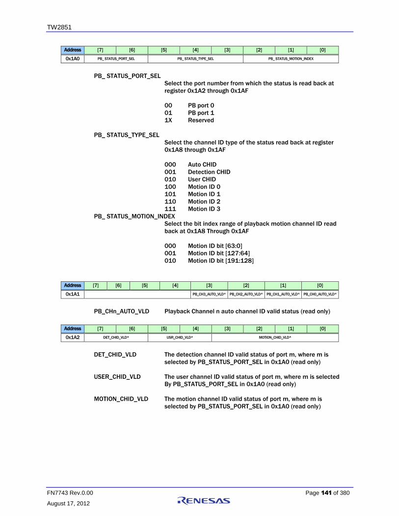
TW2851
FN7743 Rev.0.00 Page 141 of 380
August 17, 2012
Address [7] [6] [5] [4] [3] [2] [1] [0]
0x1A0 PB_ STATUS_PORT_SEL PB_ STATUS_TYPE_SEL PB_ STATUS_MOTION_INDEX
PB_ STATUS_PORT_SEL
Select the port number from which the status is read back at
register 0x1A2 through 0x1AF
00 PB port 0
01 PB port 1
1X Reserved
PB_ STATUS_TYPE_SEL
Select the channel ID type of the status read back at register
0x1A8 through 0x1AF
000 Auto CHID
001 Detection CHID
010 User CHID
100 Motion ID 0
101 Motion ID 1
110 Motion ID 2
111 Motion ID 3
PB_ STATUS_MOTION_INDEX
Select the bit index range of playback motion channel ID read
back at 0x1A8 Through 0x1AF
000 Motion ID bit [63:0]
001 Motion ID bit [127:64]
010 Motion ID bit [191:128]
Address [7] [6] [5] [4] [3] [2] [1] [0]
0x1A1 PB_CH3_AUTO_VLD* PB_CH2_AUTO_VLD* PB_CH1_AUTO_VLD* PB_CH0_AUTO_VLD*
PB_CHn_AUTO_VLD Playback Channel n auto channel ID valid status (read only)
Address [7] [6] [5] [4] [3] [2] [1] [0]
0x1A2 DET_CHID_VLD* USR_CHID_VLD* MOTION_CHID_VLD*
DET_CHID_VLD The detection channel ID valid status of port m, where m is
selected by PB_STATUS_PORT_SEL in 0x1A0 (read only)
USER_CHID_VLD The user channel ID valid status of port m, where m is selected
By PB_STATUS_PORT_SEL in 0x1A0 (read only)
MOTION_CHID_VLD The motion channel ID valid status of port m, where m is
selected by PB_STATUS_PORT_SEL in 0x1A0 (read only)

TW2851
FN7743 Rev.0.00 Page 142 of 380
August 17, 2012
Address [7] [6] [5] [4] [3] [2] [1] [0]
0x1A3 PB_CHID_LINE_SIZE_DET* PB_ANA_CHID_BW_DET
PB_CHID_LINE_SIZE_DET
The detected VBI line size of port m, where m is selected by
PB_STATUS_PORT_SEL in 0x1A0 (read only)
PB_ANA_CHID_BW_DET
The detected VBI pixel width of port m, where m is selected by
PB_STATUS_PORT_SEL in 0x1A0 (read only)
Address [7] [6] [5] [4] [3] [2] [1] [0]
0x1A4 PB_PIC_TYPE*
PB_PIC_TYPE The detected VBI picture type of port m, where m is selected by
PB_STATUS_PORT_SEL in 0x1A0 (read only)
Address [7] [6] [5] [4] [3] [2] [1] [0]
0x1A5 0 0 0 0 PB_CHID_TYPE
PB_CHID_TYPE The detected VBI channel ID type of port m, where m is selected
By PB_STATUS_PORT_SEL in 0x1A0 (read only)
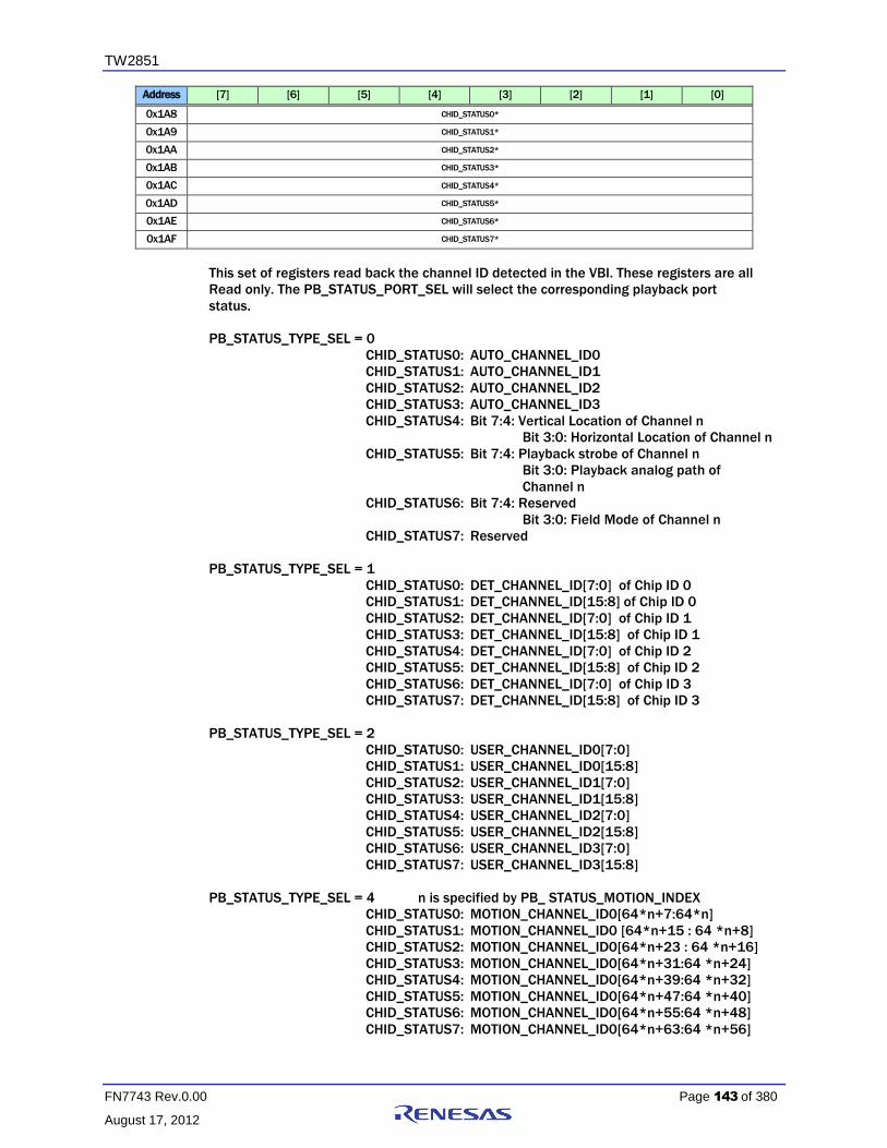
TW2851
FN7743 Rev.0.00 Page 143 of 380
August 17, 2012
Address [7] [6] [5] [4] [3] [2] [1] [0]
0x1A8 CHID_STATUS0*
0x1A9 CHID_STATUS1*
0x1AA CHID_STATUS2*
0x1AB CHID_STATUS3*
0x1AC CHID_STATUS4*
0x1AD CHID_STATUS5*
0x1AE CHID_STATUS6*
0x1AF CHID_STATUS7*
This set of registers read back the channel ID detected in the VBI. These registers are all
Read only. The PB_STATUS_PORT_SEL will select the corresponding playback port
status.
PB_STATUS_TYPE_SEL = 0
CHID_STATUS0: AUTO_CHANNEL_ID0
CHID_STATUS1: AUTO_CHANNEL_ID1
CHID_STATUS2: AUTO_CHANNEL_ID2
CHID_STATUS3: AUTO_CHANNEL_ID3
CHID_STATUS4: Bit 7:4: Vertical Location of Channel n
Bit 3:0: Horizontal Location of Channel n
CHID_STATUS5: Bit 7:4: Playback strobe of Channel n
Bit 3:0: Playback analog path of
Channel n
CHID_STATUS6: Bit 7:4: Reserved
Bit 3:0: Field Mode of Channel n
CHID_STATUS7: Reserved
PB_STATUS_TYPE_SEL = 1
CHID_STATUS0: DET_CHANNEL_ID[7:0] of Chip ID 0
CHID_STATUS1: DET_CHANNEL_ID[15:8] of Chip ID 0
CHID_STATUS2: DET_CHANNEL_ID[7:0] of Chip ID 1
CHID_STATUS3: DET_CHANNEL_ID[15:8] of Chip ID 1
CHID_STATUS4: DET_CHANNEL_ID[7:0] of Chip ID 2
CHID_STATUS5: DET_CHANNEL_ID[15:8] of Chip ID 2
CHID_STATUS6: DET_CHANNEL_ID[7:0] of Chip ID 3
CHID_STATUS7: DET_CHANNEL_ID[15:8] of Chip ID 3
PB_STATUS_TYPE_SEL = 2
CHID_STATUS0: USER_CHANNEL_ID0[7:0]
CHID_STATUS1: USER_CHANNEL_ID0[15:8]
CHID_STATUS2: USER_CHANNEL_ID1[7:0]
CHID_STATUS3: USER_CHANNEL_ID1[15:8]
CHID_STATUS4: USER_CHANNEL_ID2[7:0]
CHID_STATUS5: USER_CHANNEL_ID2[15:8]
CHID_STATUS6: USER_CHANNEL_ID3[7:0]
CHID_STATUS7: USER_CHANNEL_ID3[15:8]
PB_STATUS_TYPE_SEL = 4 n is specified by PB_ STATUS_MOTION_INDEX
CHID_STATUS0: MOTION_CHANNEL_ID0[64*n+7:64*n]
CHID_STATUS1: MOTION_CHANNEL_ID0 [64*n+15 : 64 *n+8]
CHID_STATUS2: MOTION_CHANNEL_ID0[64*n+23 : 64 *n+16]
CHID_STATUS3: MOTION_CHANNEL_ID0[64*n+31:64 *n+24]
CHID_STATUS4: MOTION_CHANNEL_ID0[64*n+39:64 *n+32]
CHID_STATUS5: MOTION_CHANNEL_ID0[64*n+47:64 *n+40]
CHID_STATUS6: MOTION_CHANNEL_ID0[64*n+55:64 *n+48]
CHID_STATUS7: MOTION_CHANNEL_ID0[64*n+63:64 *n+56]

TW2851
FN7743 Rev.0.00 Page 144 of 380
August 17, 2012
PB_STATUS_TYPE_SEL = 5 n is specified by PB_ STATUS_MOTION_INDEX
CHID_STATUS0: MOTION_CHANNEL_ID1[64*n+7:64*n],
CHID_STATUS1: MOTION_CHANNEL_ID1[64*n+15:64*
n+8]
CHID_STATUS2: MOTION_CHANNEL_ID1[64*n+23:64* n+16]
CHID_STATUS3: MOTION_CHANNEL_ID1[64*n+31:64* n+24]
CHID_STATUS4: MOTION_CHANNEL_ID1[64*n+39:64* n+32]
CHID_STATUS5: MOTION_CHANNEL_ID1[64*n+47:64* n+40]
CHID_STATUS6: MOTION_CHANNEL_ID1[64*n+55:64* n+48]
CHID_STATUS7: MOTION_CHANNEL_ID1[64*n+63:64* n+56]
PB_STATUS_TYPE_SEL = 6 n is specified by PB_ STATUS_MOTION_INDEX
CHID_STATUS0: MOTION_CHANNEL_ID2[64*n+7:64*n]
CHID_STATUS1: MOTION_CHANNEL_ID2[64*n+15:64* n+8]
CHID_STATUS2: MOTION_CHANNEL_ID2[64*n+23:64* n+16]
CHID_STATUS3: MOTION_CHANNEL_ID2[64*n+31:64* n+24]
CHID_STATUS4: MOTION_CHANNEL_ID2[64*n+39:64* n+32]
CHID_STATUS5: MOTION_CHANNEL_ID2[64*n+47:64* n+40]
CHID_STATUS6: MOTION_CHANNEL_ID2[64*n+55:64* n+48]
CHID_STATUS7: MOTION_CHANNEL_ID2[64*n+63:64* n+56]
PB_STATUS_TYPE_SEL = 7 n is specified by PB_ STATUS_MOTION_INDEX
CHID_STATUS0: MOTION_CHANNEL_ID3[64*n+7:64*n],
CHID_STATUS1: MOTION_CHANNEL_ID3[64*n+15:64* n+8]
CHID_STATUS2: MOTION_CHANNEL_ID3[64*n+23:64* n+16]
CHID_STATUS3: MOTION_CHANNEL_ID3[64*n+31:64* n+24]
CHID_STATUS4: MOTION_CHANNEL_ID3[64*n+39:64* n+32]
CHID_STATUS5: MOTION_CHANNEL_ID3[64*n+47:64 *n+40]
CHID_STATUS6: MOTION_CHANNEL_ID3[64*n+55:64* n+48]
CHID_STATUS7: MOTION_CHANNEL_ID3[64*n+63:64* n+56]
PLAYBACK CROPPING
Address [7] [6] [5] [4] [3] [2] [1] [0]
0x124 PB0_HDELAY[7:0]
0x125 PB0_HACTIVE[7:0]
0x126 0 PB0_HACTIVE[10:8] 0 PB0_HDELAY[10:8]
0x134 PB1_HDELAY[7:0]
0x135 PB1_HACTIVE[7:0]
0x136 0 PB1_HACTIVE[10:8] 0 PB1_HDELAY[10:8]
0x144 PB2_HDELAY[7:0]
0x145 PB2_HACTIVE[7:0]
0x146 0 PB2_HACTIVE[10:8] 0 PB2_HDELAY[10:8]
0x154 PB3_HDELAY[7:0]
0x155 PB3_HACTIVE[7:0]
0x156 0 PB3_HACTIVE[10:8] 0 PB3_HDELAY[10:8]
PBn_HDELAY Specify the starting pixel number for cropping port n. Pixels before
this pixel number are cropped. Note that this is before the further
cropping based on picture type.
PBn_HACTIVE Specify the active horizontal length for cropping port n. Pixels
beyond the range of this horizontal length are cropped. Note that
this is before the further cropping based on picture type.
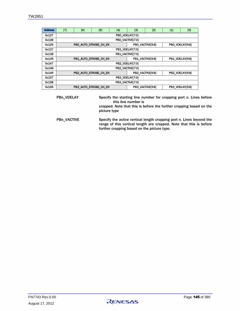
TW2851
FN7743 Rev.0.00 Page 145 of 380
August 17, 2012
Address [7] [6] [5] [4] [3] [2] [1] [0]
0x127 PB0_VDELAY[7:0]
0x128 PB0_VACTIVE[7:0]
0x129 PB0_AUTO_STROBE_CH_EN PB0_VACTIVE[9:8] PB0_VDELAY[9:8]
0x137 PB1_VDELAY[7:0]
0x138 PB1_VACTIVE[7:0]
0x139 PB1_AUTO_STROBE_CH_EN PB1_VACTIVE[9:8] PB1_VDELAY[9:8]
0x147 PB2_VDELAY[7:0]
0x148 PB2_VACTIVE[7:0]
0x149 PB2_AUTO_STROBE_CH_EN PB2_VACTIVE[9:8] PB2_VDELAY[9:8]
0x157 PB3_VDELAY[7:0]
0x158 PB3_VACTIVE[7:0]
0x159 PB3_AUTO_STROBE_CH_EN PB3_VACTIVE[9:8] PB3_VDELAY[9:8]
PBn_VDELAY Specify the starting line number for cropping port n. Lines before
this line number is
cropped. Note that this is before the further cropping based on the
picture type
PBn_VACTIVE Specify the active vertical length cropping port n. Lines beyond the
range of this vertical length are cropped. Note that this is before
further cropping based on the picture type.
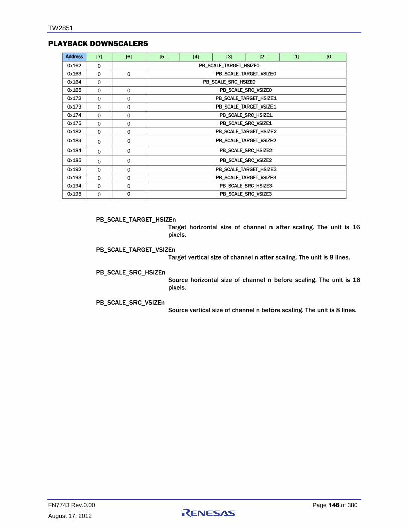
TW2851
FN7743 Rev.0.00 Page 146 of 380
August 17, 2012
PLAYBACK DOWNSCALERS
Address [7] [6] [5] [4] [3] [2] [1] [0]
0x162 0 PB_SCALE_TARGET_HSIZE0
0x163 0 0 PB_SCALE_TARGET_VSIZE0
0x164 0 PB_SCALE_SRC_HSIZE0
0x165 0 0 PB_SCALE_SRC_VSIZE0
0x172 0 0 PB_SCALE_TARGET_HSIZE1
0x173 0 0 PB_SCALE_TARGET_VSIZE1
0x174 0 0 PB_SCALE_SRC_HSIZE1
0x175 0 0 PB_SCALE_SRC_VSIZE1
0x182 0 0 PB_SCALE_TARGET_HSIZE2
0x183 0 0 PB_SCALE_TARGET_VSIZE2
0x184 0 0 PB_SCALE_SRC_HSIZE2
0x185 0 0 PB_SCALE_SRC_VSIZE2
0x192 0 0 PB_SCALE_TARGET_HSIZE3
0x193 0 0 PB_SCALE_TARGET_VSIZE3
0x194 0 0 PB_SCALE_SRC_HSIZE3
0x195 0 0 PB_SCALE_SRC_VSIZE3
PB_SCALE_TARGET_HSIZEn
Target horizontal size of channel n after scaling. The unit is 16
pixels.
PB_SCALE_TARGET_VSIZEn
Target vertical size of channel n after scaling. The unit is 8 lines.
PB_SCALE_SRC_HSIZEn
Source horizontal size of channel n before scaling. The unit is 16
pixels.
PB_SCALE_SRC_VSIZEn
Source vertical size of channel n before scaling. The unit is 8 lines.

TW2851
FN7743 Rev.0.00 Page 147 of 380
August 17, 2012
Video Multiplexers
RECORD CONTROL
Address [7] [6] [5] [4] [3] [2] [1] [0]
0x200 0 0 RP_INP_FLD_POL RP_CC_EN 0 RP_CLK_SEL
RP_INP_FLD_POL Reverse the field polarity for record path only
RP_CC_EN[1] 1 Record Cascade Output Enable
0 Record Cascade Output Disable
This feature is not available in TW2851 rev B2. This bit is always
set to 0.
RP_CC_EN[0] 1 Record Cascade Input Enable
0 Record Cascade Input Disable
This feature is not available in TW2851 rev B2. This bit is always
set to 0.
RP_CLK_SEL Record Path Clock Selection
0 Reserved
1 27 MHz for 1 port 656, 13.5 MHz for 2 port 656 or 601
2 54 MHz for 1 port 656, 27 MHz for 2 port 656 or 601
3 108 MHz for 1 port 656, 54 MHz for 2 port 656, 601, or
1120
Address [7] [6] [5] [4] [3] [2] [1] [0]
0x201 RP_BLANK_COLR RP_BGND_COLR 0 RP_BLNK_DIS 0 0
RP_BLANK_COLR The blank color of the video window that does not have active
video source or forced to show the blank color
0 Dark Gray
1 Intermediate Gray
2 Bright Gray
3 Blue
RP_BGND_COLR The background color outside of the video window configured
picture.
0 Dark Gray
1 Intermediate Gray
2 Bright Gray
3 Blue
RP_BLNK_DIS 0 Shows blank color specified by RP_BLANK_COLR
when NO_VIDEO signal is detected
1 shows the last image captured when the NO_VIDEO is
detected
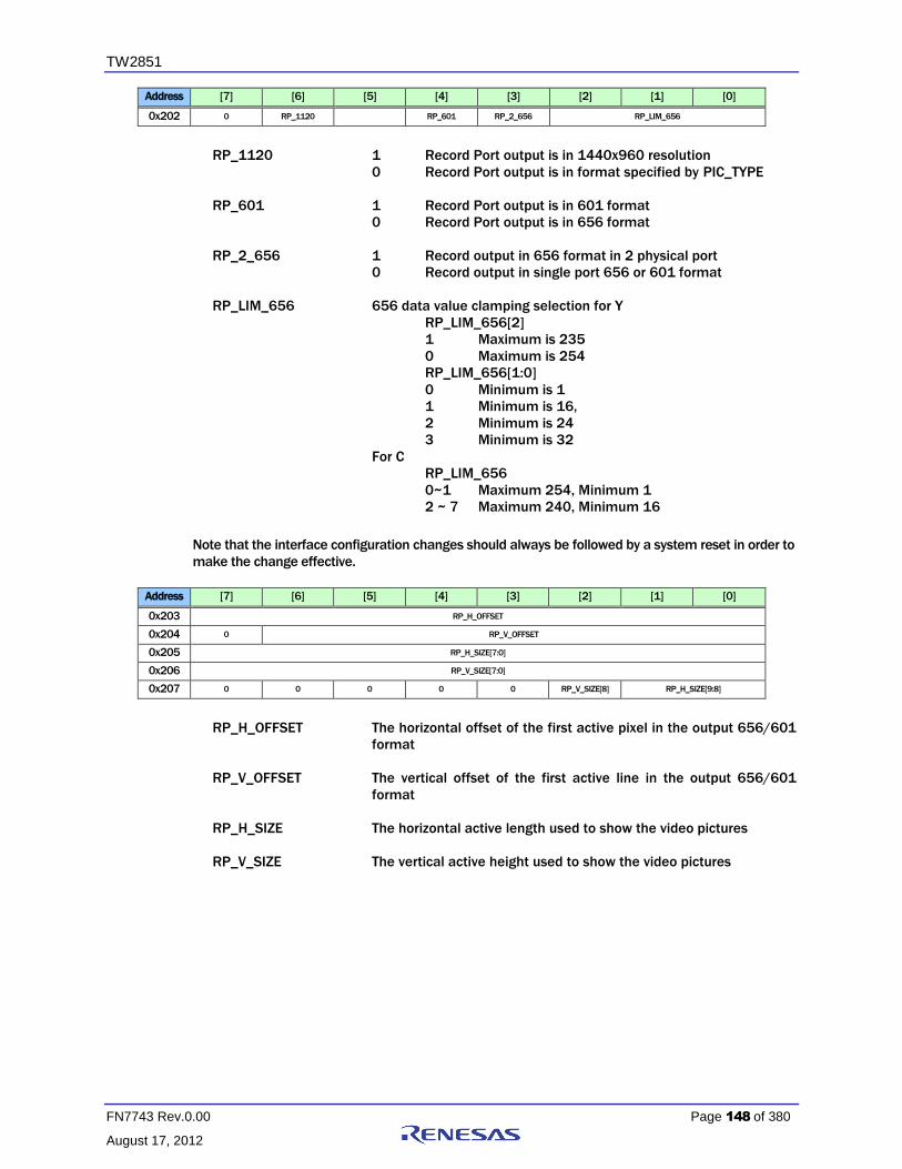
TW2851
FN7743 Rev.0.00 Page 148 of 380
August 17, 2012
Address [7] [6] [5] [4] [3] [2] [1] [0]
0x202 0 RP_1120 RP_601 RP_2_656 RP_LIM_656
RP_1120 1 Record Port output is in 1440x960 resolution
0 Record Port output is in format specified by PIC_TYPE
RP_601 1 Record Port output is in 601 format
0 Record Port output is in 656 format
RP_2_656 1 Record output in 656 format in 2 physical port
0 Record output in single port 656 or 601 format
RP_LIM_656 656 data value clamping selection for Y
RP_LIM_656[2]
1 Maximum is 235
0 Maximum is 254
RP_LIM_656[1:0]
0 Minimum is 1
1 Minimum is 16,
2 Minimum is 24
3 Minimum is 32
For C
RP_LIM_656
0~1 Maximum 254, Minimum 1
2 ~ 7 Maximum 240, Minimum 16
Note that the interface configuration changes should always be followed by a system reset in order to
make the change effective.
Address [7] [6] [5] [4] [3] [2] [1] [0]
0x203 RP_H_OFFSET
0x204 0 RP_V_OFFSET
0x205 RP_H_SIZE[7:0]
0x206 RP_V_SIZE[7:0]
0x207 0 0 0 0 0 RP_V_SIZE[8] RP_H_SIZE[9:8]
RP_H_OFFSET The horizontal offset of the first active pixel in the output 656/601
format
RP_V_OFFSET The vertical offset of the first active line in the output 656/601
format
RP_H_SIZE The horizontal active length used to show the video pictures
RP_V_SIZE The vertical active height used to show the video pictures

TW2851
FN7743 Rev.0.00 Page 149 of 380
August 17, 2012
Address [7] [6] [5] [4] [3] [2] [1] [0]
0x210 RP_CH_EN_0 0 RP_FUNC_MD_0 RP_ANA_0 0 RP_BLNK_0 RP_MIR_V_0 RP_MIR_H_0
0x211 RP_CH_EN_1 0 RP_FUNC_MD_1 RP_ANA_1 0 RP_BLNK_1 RP_MIR_V_1 RP_MIR_H_1
0x212 RP_CH_EN_2 0 RP_FUNC_MD_2 RP_ANA_2 0 RP_BLNK_2 RP_MIR_V_2 RP_MIR_H_2
0x213 RP_CH_EN_3 0 RP_FUNC_MD_3 RP_ANA_3 0 RP_BLNK_3 RP_MIR_V_3 RP_MIR_H_3
RP_CH_EN Channel Enable Control for each of channel 0 through 3
1 Enable channel
0 Disable channel
RP_FUNC_MD When the Record Path is not in Switch mode, this bit specifies the
record capture mode
1 Strobe Mode
0 Live Mode
RP_ANA Specify the analog input selection of each of the channel.
0 VINA
1 VINB
RP_BLNK Force the channel to display blank color
1 Blank
0 Normal video
RP_MIR_V Control to mirror the image vertically for each channel
0 Do not mirror vertically
1 Mirror vertically
RP_MIR_H Control to mirror the image horizontally for each channel
0 Do not mirror horizontally
1 Mirror horizontally
Address [7] [6] [5] [4] [3] [2] [1] [0]
0x214 0 0 0 0 RP_STROBE_3 RP_STROBE_2 RP_STROBE_1 RP_STROBE_0
RP_STROBE Strobe command for each channel. Once set to 1, the
corresponding channel will capture one field/frame and then clear
this bit.

TW2851
FN7743 Rev.0.00 Page 150 of 380
August 17, 2012
Address [7] [6] [5] [4] [3] [2] [1] [0]
0x215 0 RP_STRB_FLD RP_CH_CYCLE RP_SM_EN RP_PIC_TYPE
RP_STRB_FLD In non-switch mode, this bit controls which field to capture in field
mode ( pic_type 0, 2, 4, 6, 7)
0 Capture Even field
1 Capture Odd field
RP_CH_CYCLE In non-switch mode, this RP_CH_CYCLE controls how many
channels to interleave when the pic_type is 0, 1, 6, and 7.
PIC_TYPE 0, 1
0 Capture and interleave channel 0, 1, 2, 3
1 Capture channel 0
2 Capture and interleave channel 0, 1
3 Capture and interleave channel 0, 1, 2
PIC_TYPE 6, 7
1 Capture channel 0, 1
2 Capture and interleave channel 0, 1, 2, 3
RP_SM_EN 1 Record Path is in Switch Queue Mode
0 Record Path is in Live or Strobe Mode
RP_PIC_TYPE When Record Path is not in Switch Queue Mode, RP_PIC_TYPE
specifies the pic_type used in LIVE/Strobe mode
RECORD SWITCH QUEUE
Address [7] [6] [5] [4] [3] [2] [1] [0]
0x208 RP_SQ_CMD RP_SQ_WR RP_SQ_RW_DONE* 0 0 0 0 RP_CONFIG_DONE
RP_SQ_CMD The command bit to start a Record Path Switch Queue read / write
operation. Set to 1 to start a command. This bit will self clear.
RP_SQ_WR Read/Write Flag for Record Path Switch Queue operation
1 Write to Switch Queue
0 Read from Switch Queue
RP_SQ_RW_DONE Read Only
RP_CONFIG_DONE After any configuration changes are made to the record path
control registers, this bit should be set to resume the record path
operation.

TW2851
FN7743 Rev.0.00 Page 151 of 380
August 17, 2012
Address [7] [6] [5] [4] [3] [2] [1] [0]
0x209 RP_SQ_ DATA[7:0]
0x20A RP_SQ_ DATA[15:8]
0x20B RP_SQ_ DATA[23:16]
0x20C RP_SQ_ DATA[31:24]
RP_SQ_DATA0 ~ 3 are used to read/write the data from/to the record path switch queue
entry when a switch queue read/write operation is performed.
In write operation, these 4 registers are written first. Then a command is issued using
RP_SQ_CMD in 0x208 to move the data into the switching queue.
In read operation, a read command is issued using RP_SQ_CMD in 0x208 to move the
data from switch queue into these 4 registers. The MCU can then read the entry from
these registers.
The definition of each bit used in the switch queue entry is as follows.
RP_SQ_DATA[1:0] Port ID for channel 0 (upper left window)
RP_SQ_DATA[3:2] Chip ID for channel 0
RP_SQ_DATA[5:4] Port ID for Channel 1 (upper right window)
RP_SQ_DATA[7:6] Chip ID for Channel 1
RP_SQ_DATA[9:8] Port ID for Channel 2 (Lower left window)
RP_SQ_DATA[11:10] Chip ID for Channel 2
RP_SQ_DATA[13:12] Port ID for Channel 3 (Lower right window)
RP_SQ_DATA[15:14] Chip ID for Channel 3
RP_SQ_DATA[19:16] Channel 0 ~ 3 disable bit.
Bit 16 set to 1, Channel 0 is disabled.
Bit 17 set to 1, Channel 1 is disabled
Bit 18 set to 1, Channel 2 is disabled
Bit 19 set to 1, Channel 3 is disabled
RP_SQ_DATA[22:20] Picture Type, as shown in Figure 15
RP_SQ_DATA[23] Strobe field type for field mode picture type.
1 Odd field
0 Even field
RP_SQ_DATA[25:24] Field/Frame based OSD0 selection for Record Output Port 0. There
will be 4 sets of OSD0 configuration information. These 2 bits
selects one of the 4 sets for record output port 0. According to
the setting of these 2 bits, the OSD result can change from field to
field or frame to frame.
RP_SQ_DATA[27:26] Field/Frame based OSD1 selection for Record Output Port 1. There
will be 4 sets of OSD1 configuration information. These 2 bits
selects one of the 4 sets for record output port 1. According to the
setting of these 2 bits, the OSD result can change from field to field
or frame to frame.
RP_SQ_DATA[31:28] Reserved

TW2851
FN7743 Rev.0.00 Page 152 of 380
August 17, 2012
Address [7] [6] [5] [4] [3] [2] [1] [0]
0x20D RP_SQ_ ADDR[7:0]
0x20E RP_SQ_ SIZE[7:0]
0x20F 0 RP_SQ_SIZE[10:8] 0 RP_SQ_ADDR[10:8]
RP_SQ_ADDR The switch queue entry address to perform the switch queue
read / write command. This address is automatically incremented
after the command is performed
RP_SQ_SIZE The switch queue size.
1-2047: 1-2047
2048: 0
RECORD CHID ENCODER
Address [7] [6] [5] [4] [3] [2] [1] [0]
0x216 RP_MOTN_ID_EN RP_DIG_ID_EN RP_ANA_ID_EN RP_ANA_RIC_EN RP_AUTO_ID_EN RP_AUTO_RPT_EN RP_DET_ID_EN RP_USR_ID_EN
RP_MOTN_ID_EN 1 Turn on motion information encoding
0 Do not turn on motion information encoding
RP_DIG_ID_EN 1 Turn on the digital channel ID encoding
0 Turn off the digital channel ID encoding
RP_ANA_ID_EN 1 Turn on the analog channel ID encoding
0 Turn off the analog channel ID encoding
RP_ANA_RPT_EN 1 Turn on the analog auto channel ID repeat line
0 Turn off the analog auto channel ID repeat line
RP_AUTO_ID_EN 1 Turn on the auto channel ID encoding
0 Turn off the auto channel ID encoding
RP_DET_ID_EN 1 Turn on the detection ID encoding
0 Turn off the detection ID encoding
RP_USR_ID_EN 1 Turn on the user information encoding
0 Turn off the user information encoding
Address [7] [6] [5] [4] [3] [2] [1] [0]
0x217 RP_ANA_CHID_H_OFST
RP_ANA_CHID_H_OFST
The horizontal starting offset for Analog Channel ID
Address [7] [6] [5] [4] [3] [2] [1] [0]
0x218 RP_ANA_CHID_HIGH
0x219 RP_ANA_CHID_LOW
RP_ANA_CHID_HIGH Pixel values bigger than this setting are interpreted as “1” for
Analog Channel ID (default: 235)
RP_ANA_CHID_LOW Pixel values smaller than this setting are interpreted as “0” for
Analog Channel ID (default: 16)
Address [7] [6] [5] [4] [3] [2] [1] [0]

TW2851
FN7743 Rev.0.00 Page 153 of 380
August 17, 2012
0x21A RP_CHID_V_OFSTO 0 RP_CHID_V_OFST
0x21B RP_CHID_V_OFSTE RP_USR_ID_PT_SEL RP_ANA_CHID_BW
RP_CHID_V_OFSTO Control the vertical starting offset on top of RP_CHID_V_OFST in
odd field for Analog Channel ID
RP_CHID_V_OFSTE Control the vertical starting offset on top of RP_CHID_V_OFST in
even field for Analog Channel ID
RP_CHID_V_OFST Vertical starting offset for Analog Channel ID. The actual vertical
line offset is RP_CHID_V_OFST + RP_CHID_V_OFSTO or
RP_CHID_V_OFST + RP_CHID_V_OFSTE
RP_ANA_CHID_BW Control the pixel width of each bit for Analog Channel ID
0 1 pixel
: :
31 32 pixels (default)
RP_USER_ID_PT_SEL This bit is used to select the user channel ID registers in 0x220 ~
0x227 information is to be used for either record port 0 or 1
0 0x220 ~ 0x227 are used for record port 0
1 0x220 ~ 0x227 are used for record port 1
Address [7] [6] [5] [4] [3] [2] [1] [0]
0x21C RP_SMALL_FR RP_BI_CLK RP_BYPASS RP_GEN_CTL
RP_GEN_CTL Internal test function
RP_BYPASS Enable bypass from video decoder to record output pin with byte-
interleaving format
0 Disable bypass
1 Enable bypass
RP_BI_CLK Use 27 MHz CLKOY and CLKOYB for Byte Interleaving Output. This
bit is valid only when RP_BYPASS is set to 1.
0 27 MHz
1 54 MHz
RP_SMALL_FR Internal test function
Address [7] [6] [5] [4] [3] [2] [1] [0]
0x21D RP_CHNUM1 RP_CHNUM0
0x21E RP_CHNUM3 RP_CHNUM2
0x21F RP_GEN_FLDPOL
RP_CHNUM The Channel Number to display in non-switch mode
[3:2] CHIP ID
[1:0] PORT ID
RP_GEN_FLDPOL Reverse the field polarity of the internal pattern generator for RP
path.
Address [7] [6] [5] [4] [3] [2] [1] [0]

TW2851
FN7743 Rev.0.00 Page 154 of 380
August 17, 2012
0x220 RP_USER_CHID[7:0]
0x221 RP_USER_CHID[15:8]
0x222 RP_USER_CHID[23:16]
0x223 RP_USER_CHID[31:24]
0x224 RP_USER_CHID[39:32]
0x225 RP_USER_CHID[47:40]
0x226 RP_USER_CHID[55:48]
0x227 RP_USER_CHID[63:56]
RP_USER_CHID Used to set the USER Channel ID for record path.
Depending on the RP_USER_ID_PT_SEL (0x21B bit 5), these can
be used to read/write the user channel ID for record port 0,
or record port 1. Always set RP_USER_ID_PT_SEL before any
read/write to these registers
DISPLAY CONTROL
Address [7] [6] [5] [4] [3] [2] [1] [0]
0x230 DP_BLANK_COLR DP_BGND_COLR
DP_BLANK_COLR[3]
1 Blue
0 Gray, the gray level is selected by
DP_BLANK_COLR[2:0]
DP_BLANK_COLR[2:0]
0 ~ 3 Black
4 Gray darkest
5 Gray darker
6 Gray lighter
7 Gray lightest
DP_BGND_COLR[3]
1 Blue
0 Gray, the gray level is selected by
DP_BGND_COLR[2:0]
DP_BGND_COLR[2:0]
0 ~ 3 Black
4 Gray darkest
5 Gray darker
6 Gray lighter
7 Gray lightest

TW2851
FN7743 Rev.0.00 Page 155 of 380
August 17, 2012
Address [7] [6] [5] [4] [3] [2] [1] [0]
0x231 DP_LIM_656 DP_CVBS_VSPOL DP_FIELD_ID DP_WINWIDTH
DP_LIM_656 656 Data Clamping
For Y:
DP_LIM_656[2]
0 Maximum limit to 254
1 Maximum limit to 235
DP_LIM_656[1:0]
0 Minimum set to 1
1 Minimum set to 16
2 Minimum set to 24
3 Minimum set to 32
For C
DP_LIM_656
0 Maximum 254, Minimum 1
1~7 Maximum 240, Minimum 16
DP_CVBS_VSPOL 0 Do not reverse the VS polarity for CVBS
1 Reverse the VS polarity for CVBS
DP_FIELD_ID 1 Force the output to de-interlacer to top field
0 Do not force field ID to top field
DP_WINWIDTH 1 1440 pixels maximum per line
0 720 pixels maximum per line
Address [7] [6] [5] [4] [3] [2] [1] [0]
0x232 DP_SOFTRST DP_DI_FLDPOL 0 0 0 0 0 0
DP_SOFTRST 1 Reset Display Path
0 Do not reset the display path
DP_DI_FLDPOL 1 Reverse the field polarity to the VGA de-interlacer
0 Do not reverse the field polarity to the de-interlacer
Address [7] [6] [5] [4] [3] [2] [1] [0]
0x237 DP_CAS_IN_EN
DP_CAS_IN_EN Enable the display cascade input
Address [7] [6] [5] [4] [3] [2] [1] [0]
0x238 1 0
Reserved

TW2851
FN7743 Rev.0.00 Page 156 of 380
August 17, 2012
Address [7] [6] [5] [4] [3] [2] [1] [0]
0x23A DP_BORDER_BLINK
DP_BORDER_BLINK 1 Turn on border blinking for the corresponding window 0
~ 7
0 Turn off border blinking
Address [7] [6] [5] [4] [3] [2] [1] [0]
0x23B DP_VGA_FLDPOL DP_CVBS_FLDPOL DP_VD_FLDPOL
DP_VGA_FLDPOL Reverse the field polarity for the display VGA output
DP_CVBS_FLDPOL Reverse the field polarity for the display CVBS output
DP_VD_FLDPOL Reverse the field polarity of the incoming video stream
Address [7] [6] [5] [4] [3] [2] [1] [0]
0x23C DP_FREEZEOPT[7:0]
0x23D DP_ADAPT_EN[7:0]
DP_FREEZEOPT 0 Display field only when freeze command is issued or
underflow condition occurs
1 Display frame when freeze command is issued or
underflow condition occurs
DP_ADAPT_EN 0 Display field/frame according to DP_FREEZEOPT
1 Overwrite DP_FREEZEOPT and display frame when
no_motion is asserted
Address [7] [6] [5] [4] [3] [2] [1] [0]
0x23E NON_REALTIME[7:0]
0x23F FRCE_BLNK_SEL FRCE_BLNK_GRY_LVL NON_REALTIME[8]
NON_REALTIME[n] 0 Display non-real-time video source at display window n,
n = 0 ~ 8. n equals 8 specifies the display cascade input.
1 Display real-time Video Sources at display window n,
n = 0 ~ 8. n equals 8 specifies the display cascade input.
FRCE_BLNK_GRY_LVL These bit only work when the DP_BLNKm Register bit is set
(0x250[0], 0x258[0], …., etc.)
0xx Black
100 25% Gray
101 40% Gray
110 75% Gray
111 100% Gray
FRCE_BLNK_SEL This bit only work when the DP_BLNKm Register bit is set (0x250[0],
0x258[0], …., etc.)
0 Gray
1 Blue
Address [7] [6] [5] [4] [3] [2] [1] [0]

TW2851
FN7743 Rev.0.00 Page 157 of 380
August 17, 2012
0x240 DP_VGA_HDELAY[7:0]
0x241 DP_VGA_HACTIVE[7:0]
0x242 DP_VGA_HACTIVE[10:8] DP_VGA_HDELAY[10:8]
0x243 DP_VGA_VDELAY[7:0]
0x244 DP_VGA_VACTIVE[7:0]
0x245 DP_VGA_VACTIVE[10:8] DP_VGA_VDELAY[10:8]
DP_VGA_HDELAY VGA Cropping HDELAY
DP_VGA_HACTIVE VGA Cropping HACTIVE
DP_VGA_VDELAY VGA Cropping VDELAY
DP_VGA_VACTIVE VGA Cropping VACTIVE
Address [7] [6] [5] [4] [3] [2] [1] [0]
0x24C DP_BORDER_COLR 0 DP_PBVD_SEL
DP_BORDER_COLR Select the color of the display window border
DP_PBVD_SEL Select the source of display window 0 ~ 3 to be from PB_CH0 ~
PB_CH3 or from video decoders VD0 ~ VD3
0 PB
1 VD
Address [7] [6] [5] [4] [3] [2] [1] [0]
0x24D DP_CHNAB_SEL
DP_CHNAB_SEL Select the Analog Switch A/B for each window 0 ~ 7
Address [7] [6] [5] [4] [3] [2] [1] [0]
0x24E DP_BORDER_EN
DP_BORDER_EN Enable display window borders for each window 0 ~ 7
Address [7] [6] [5] [4] [3] [2] [1] [0]
0x24F DP_STRB_REQ
DP_STRB_REQ Strobe Request to each of the 8 windows. Self clear after the
strobe is done
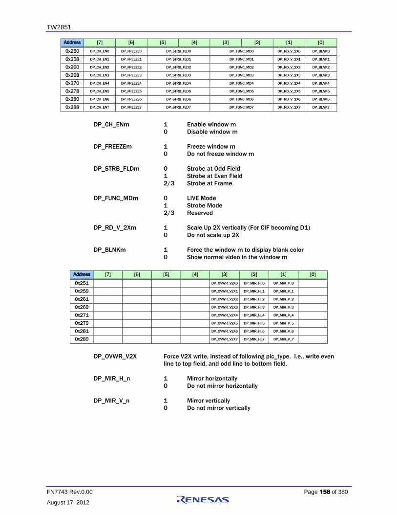
TW2851
FN7743 Rev.0.00 Page 158 of 380
August 17, 2012
Address [7] [6] [5] [4] [3] [2] [1] [0]
0x250 DP_CH_EN0 DP_FREEZE0 DP_STRB_FLD0 DP_FUNC_MD0 DP_RD_V_2X0 DP_BLNK0
0x258 DP_CH_EN1 DP_FREEZE1 DP_STRB_FLD1 DP_FUNC_MD1 DP_RD_V_2X1 DP_BLNK1
0x260 DP_CH_EN2 DP_FREEZE2 DP_STRB_FLD2 DP_FUNC_MD2 DP_RD_V_2X2 DP_BLNK2
0x268 DP_CH_EN3 DP_FREEZE3 DP_STRB_FLD3 DP_FUNC_MD3 DP_RD_V_2X3 DP_BLNK3
0x270 DP_CH_EN4 DP_FREEZE4 DP_STRB_FLD4 DP_FUNC_MD4 DP_RD_V_2X4 DP_BLNK4
0x278 DP_CH_EN5 DP_FREEZE5 DP_STRB_FLD5 DP_FUNC_MD5 DP_RD_V_2X5 DP_BLNK5
0x280 DP_CH_EN6 DP_FREEZE6 DP_STRB_FLD6 DP_FUNC_MD6 DP_RD_V_2X6 DP_BLNK6
0x288 DP_CH_EN7 DP_FREEZE7 DP_STRB_FLD7 DP_FUNC_MD7 DP_RD_V_2X7 DP_BLNK7
DP_CH_ENm 1 Enable window m
0 Disable window m
DP_FREEZEm 1 Freeze window m
0 Do not freeze window m
DP_STRB_FLDm 0 Strobe at Odd Field
1 Strobe at Even Field
2/3 Strobe at Frame
DP_FUNC_MDm 0 LIVE Mode
1 Strobe Mode
2/3 Reserved
DP_RD_V_2Xm 1 Scale Up 2X vertically (For CIF becoming D1)
0 Do not scale up 2X
DP_BLNKm 1 Force the window m to display blank color
0 Show normal video in the window m
Address [7] [6] [5] [4] [3] [2] [1] [0]
0x251 DP_OVWR_V2X0 DP_MIR_H_0 DP_MIR_V_0
0x259 DP_OVWR_V2X1 DP_MIR_H_1 DP_MIR_V_1
0x261 DP_OVWR_V2X2 DP_MIR_H_2 DP_MIR_V_2
0x269 DP_OVWR_V2X3 DP_MIR_H_3 DP_MIR_V_3
0x271 DP_OVWR_V2X4 DP_MIR_H_4 DP_MIR_V_4
0x279 DP_OVWR_V2X5 DP_MIR_H_5 DP_MIR_V_5
0x281 DP_OVWR_V2X6 DP_MIR_H_6 DP_MIR_V_6
0x289 DP_OVWR_V2X7 DP_MIR_H_7 DP_MIR_V_7
DP_OVWR_V2X Force V2X write, instead of following pic_type. I.e., write even
line to top field, and odd line to bottom field.
DP_MIR_H_n 1 Mirror horizontally
0 Do not mirror horizontally
DP_MIR_V_n 1 Mirror vertically
0 Do not mirror vertically
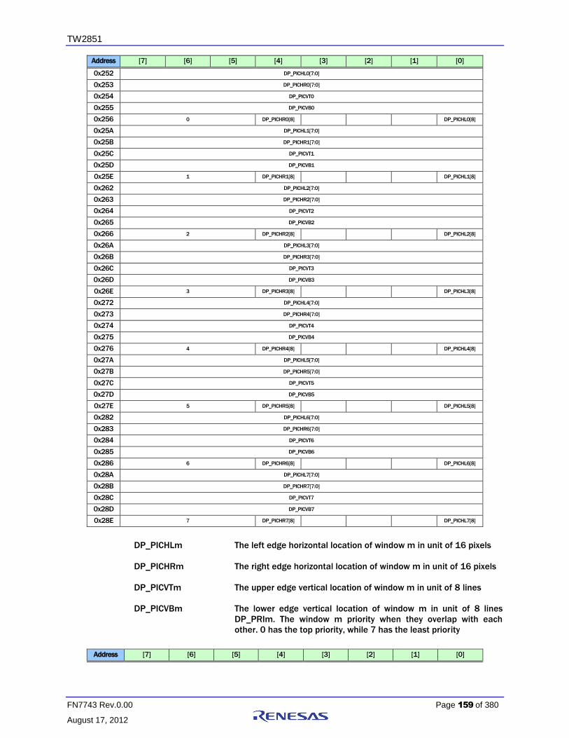
TW2851
FN7743 Rev.0.00 Page 159 of 380
August 17, 2012
Address [7] [6] [5] [4] [3] [2] [1] [0]
0x252 DP_PICHL0[7:0]
0x253 DP_PICHR0[7:0]
0x254 DP_PICVT0
0x255 DP_PICVB0
0x256 0 DP_PICHR0[8] DP_PICHL0[8]
0x25A DP_PICHL1[7:0]
0x25B DP_PICHR1[7:0]
0x25C DP_PICVT1
0x25D DP_PICVB1
0x25E 1 DP_PICHR1[8] DP_PICHL1[8]
0x262 DP_PICHL2[7:0]
0x263 DP_PICHR2[7:0]
0x264 DP_PICVT2
0x265 DP_PICVB2
0x266 2 DP_PICHR2[8] DP_PICHL2[8]
0x26A DP_PICHL3[7:0]
0x26B DP_PICHR3[7:0]
0x26C DP_PICVT3
0x26D DP_PICVB3
0x26E 3 DP_PICHR3[8] DP_PICHL3[8]
0x272 DP_PICHL4[7:0]
0x273 DP_PICHR4[7:0]
0x274 DP_PICVT4
0x275 DP_PICVB4
0x276 4 DP_PICHR4[8] DP_PICHL4[8]
0x27A DP_PICHL5[7:0]
0x27B DP_PICHR5[7:0]
0x27C DP_PICVT5
0x27D DP_PICVB5
0x27E 5 DP_PICHR5[8] DP_PICHL5[8]
0x282 DP_PICHL6[7:0]
0x283 DP_PICHR6[7:0]
0x284 DP_PICVT6
0x285 DP_PICVB6
0x286 6 DP_PICHR6[8] DP_PICHL6[8]
0x28A DP_PICHL7[7:0]
0x28B DP_PICHR7[7:0]
0x28C DP_PICVT7
0x28D DP_PICVB7
0x28E 7 DP_PICHR7[8] DP_PICHL7[8]
DP_PICHLm The left edge horizontal location of window m in unit of 16 pixels
DP_PICHRm The right edge horizontal location of window m in unit of 16 pixels
DP_PICVTm The upper edge vertical location of window m in unit of 8 lines
DP_PICVBm The lower edge vertical location of window m in unit of 8 lines
DP_PRIm. The window m priority when they overlap with each
other. 0 has the top priority, while 7 has the least priority
Address [7] [6] [5] [4] [3] [2] [1] [0]

TW2851
FN7743 Rev.0.00 Page 160 of 380
August 17, 2012
0x257 DP_WR_CH_EN[8] DP_WR_EN
0x267 DP_WR_CH_EN[7:0]
DP_WR_EN Enable write to the display buffer. This bit is combined with
DP_WR_CH_EN ({0x257[4], 0x267[7:0]} for the per window control.
I.e., use DP_WR_CH_EN to select which windows will be controlled, and
then use DP_WR_EN to do the actual enable / disable.
DP_WR_CH_EN {0x257[4], 0x267[7:0]} controls per-window display write buffer
control. These bit work together with 0x257[0].
Address [7] [6] [5] [4] [3] [2] [1] [0]
0x27F DP_BASE_ADDR
DP_BASE_ADDR The base address of the display buffer. In unit of 128 Kbytes
The DDR address generated with DP_BASE_ADDR is
{DP_BASE_ADDR, 17’h0}
Address [7] [6] [5] [4] [3] [2] [1] [0]
0x28F DP_TEST
DP_TEST Default 0

TW2851
FN7743 Rev.0.00 Page 161 of 380
August 17, 2012
SPOT CONTROL
Address [7] [6] [5] [4] [3] [2] [1] [0]
0x290 0 0 SP_INP_FLD_POL SP_CC_EN
SP_INP_FLD_POL Reverse the field polarity for spot path only
SP_CC_EN[1] 1 SPOT Cascade Output Enable
0 SPOT Cascade Output Disable
SP_CC_EN[0] 1 SPOT Cascade Input Enable. The SPOT clock is the
clock from SPOT cascade input clock.
0 SPOT Cascade Input Disable. The SPOT clock is
a 27 MHz clock generated internally
Address [7] [6] [5] [4] [3] [2] [1] [0]
0x291 SP_BLANK_COLR SP_BGND_COLR SP_BLANK_MODE SP_BORDER_EN 0
SP_BLANK_COLR The blank color of the video window that does not have active
video source or forced to show the blank color
0 Dark Gray
1 Intermediate Gray
2 Bright Gray
3 Blue
SP_BGND_COLR The background color outside of the video window configured
picture.
0 Dark Gray
1 Intermediate Gray
2 Bright Gray
3 Blue
SP_BLANK_MODE 0 Show blank color as specified by SP_BLANK_COLR
When the NO_VIDEO is detected
1 Shows the last image captured when the NO_VIDEO is
detected
2 Display blank color specified by SP_BLANK_COLR with
border blinking when NO_VIDEO is detected (valid only if
SP_BORDER_EN is on)
3 Display the last image captured with border blinking
when the NO_VIDEO is detected (valid only if
SP_BORDER_EN is on)
SP_BORDER_EN 1 Enable displaying SPOT border
0 Disable displaying SPOT border

TW2851
FN7743 Rev.0.00 Page 162 of 380
August 17, 2012
Address [7] [6] [5] [4] [3] [2] [1] [0]
0x292 SP_BORDER_COLR 0 0 SP_LIM_656
SP_LIM_656 656 data value clamping selection
For Y
SP_LIM_656[2]
1 Maximum is 235
0 Maximum is 254
SP_LIM_656[1:0]
0 Minimum is 1
1 Minimum is 16,
2 Minimum is 24
3 Minimum is 32
For C
SP_LIM_656
0~1 Maximum 254, Minimum 1
2 ~ 7 Maximum 240, Minimum 16
SP_BORDER_COLR
0 Black
1 Dark gray
2 Light gray
3 White
Address [7] [6] [5] [4] [3] [2] [1] [0]
0x293 SP_H_OFFSET
0x294 0 SP_V_OFFSET
0x295 SP_H_SIZE[7:0]
0x296 SP_V_SIZE[7:0]
0x297 0 0 0 0 0 SP_V_SIZE[8] SP_H_SIZE[9:8]
SP_H_OFFSET The horizontal offset of the first active pixel in the output 656/601
format
SP_V_OFFSET The vertical offset of the first active line in the output 656/601
format
SP_H_SIZE The horizontal active length used to show the video pictures
SP_V_SIZE The vertical active height used to show the video pictures

TW2851
FN7743 Rev.0.00 Page 163 of 380
August 17, 2012
Address [7] [6] [5] [4] [3] [2] [1] [0]
0x2A0 SP_CH_EN_0 SP_FREEZE_0 SP_FUNC_MD_0 SP_ANA_0 0 SP_BLNK_0 SP_MIR_V_0 SP_MIR_H_0
0x2A1 SP_CH_EN_1 SP_FREEZE_1 SP_FUNC_MD_1 SP_ANA_1 0 SP_BLNK_1 SP_MIR_V_1 SP_MIR_H_1
0x2A2 SP_CH_EN_2 SP_FREEZE_2 SP_FUNC_MD_2 SP_ANA_2 0 SP_BLNK_2 SP_MIR_V_2 SP_MIR_H_2
0x2A3 SP_CH_EN_3 SP_FREEZE_3 SP_FUNC_MD_3 SP_ANA_3 0 SP_BLNK_3 SP_MIR_V_3 SP_MIR_H_3
SP_CH_EN Channel Enable Control for each of channel 0 through 3
1 Enable channel
0 Disable channel
SP_FREEZE 1 Freeze the video
0 Disable freeze
SP_FUNC_MD When the SPOT Path is not in Switch mode, this bit specifies the
SPOT mode of
1 Strobe Mode
0 Live Mode
SP_ANA Specify the analog input selection of each of the channel.
0 VINA
1 VINB
SP_BLNK Force the channel to display blank color
1 Blank Color
0 Normal video
SP_MIR_V Control to mirror the image vertically for each channel
0 Do not mirror vertically
1 Mirror vertically
SP_MIR_H Control to mirror the image horizontally for each channel
0 Do not mirror horizontally
1 Mirror horizontally
Address [7] [6] [5] [4] [3] [2] [1] [0]
0x2A4 0 0 0 0 SP_STROBE_3 SP_STROBE_2 SP_STROBE_1 SP_STROBE_0
SP_STROBE Strobe command for each channel. Once set to 1, the
corresponding channel will capture one field/frame and then clear
this bit.
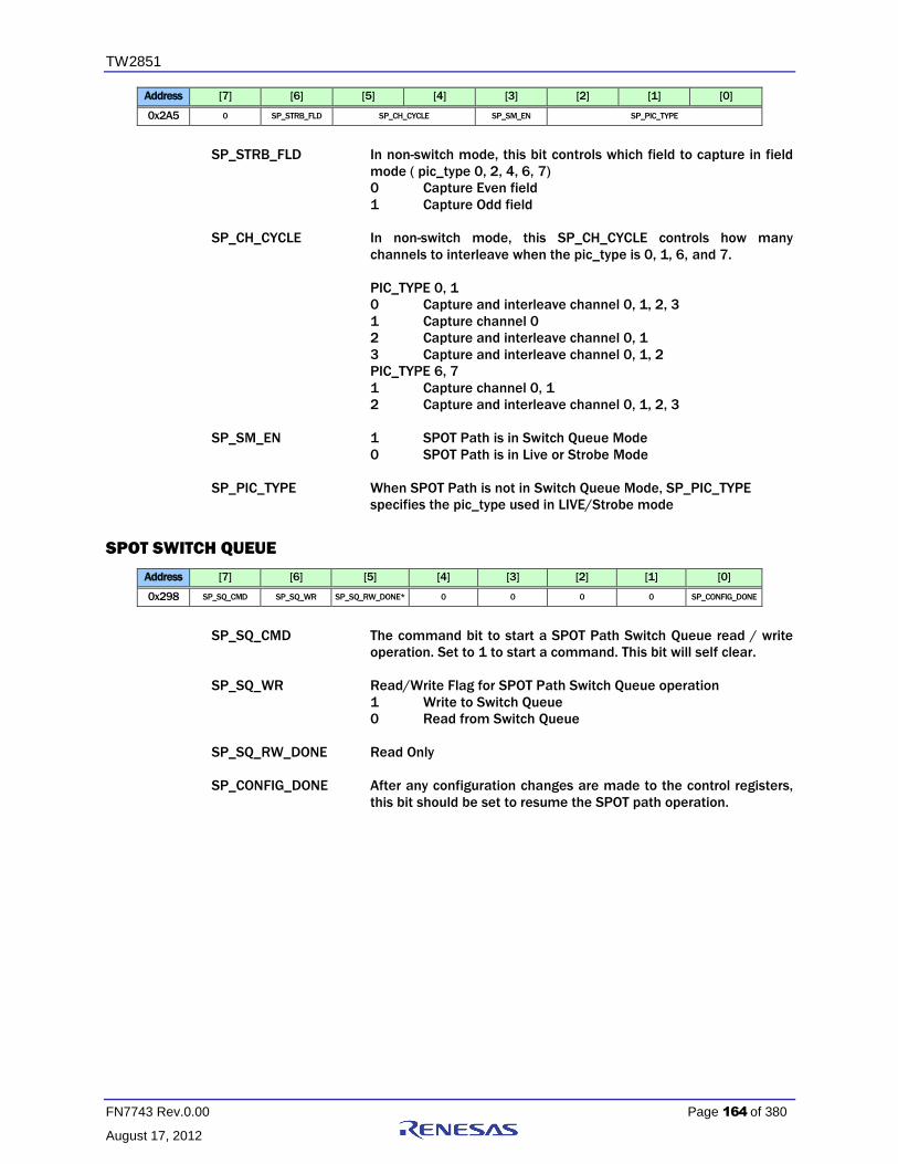
TW2851
FN7743 Rev.0.00 Page 164 of 380
August 17, 2012
Address [7] [6] [5] [4] [3] [2] [1] [0]
0x2A5 0 SP_STRB_FLD SP_CH_CYCLE SP_SM_EN SP_PIC_TYPE
SP_STRB_FLD In non-switch mode, this bit controls which field to capture in field
mode ( pic_type 0, 2, 4, 6, 7)
0 Capture Even field
1 Capture Odd field
SP_CH_CYCLE In non-switch mode, this SP_CH_CYCLE controls how many
channels to interleave when the pic_type is 0, 1, 6, and 7.
PIC_TYPE 0, 1
0 Capture and interleave channel 0, 1, 2, 3
1 Capture channel 0
2 Capture and interleave channel 0, 1
3 Capture and interleave channel 0, 1, 2
PIC_TYPE 6, 7
1 Capture channel 0, 1
2 Capture and interleave channel 0, 1, 2, 3
SP_SM_EN 1 SPOT Path is in Switch Queue Mode
0 SPOT Path is in Live or Strobe Mode
SP_PIC_TYPE When SPOT Path is not in Switch Queue Mode, SP_PIC_TYPE
specifies the pic_type used in LIVE/Strobe mode
SPOT SWITCH QUEUE
Address [7] [6] [5] [4] [3] [2] [1] [0]
0x298 SP_SQ_CMD SP_SQ_WR SP_SQ_RW_DONE* 0 0 0 0 SP_CONFIG_DONE
SP_SQ_CMD The command bit to start a SPOT Path Switch Queue read / write
operation. Set to 1 to start a command. This bit will self clear.
SP_SQ_WR Read/Write Flag for SPOT Path Switch Queue operation
1 Write to Switch Queue
0 Read from Switch Queue
SP_SQ_RW_DONE Read Only
SP_CONFIG_DONE After any configuration changes are made to the control registers,
this bit should be set to resume the SPOT path operation.

TW2851
FN7743 Rev.0.00 Page 165 of 380
August 17, 2012
Address [7] [6] [5] [4] [3] [2] [1] [0]
0x299 SP_SQ_ DATA[7:0]
0x29A SP_SQ_ DATA[15:8]
0x29B SP_SQ_ DATA[23:16]
SP_SQ_DATA are used to read/write the data from/to the SPOT path switch queue entry
when a switch queue read/write operation is performed.
In write operation, these 4 registers are written first. Then a command is issued using
SP_SQ_CMD in 0x298 to move the data into the switching queue.
In read operation, a read command is issued using SP_SQ_CMD in 0x298 to move the
data from switch queue into these 4 registers. The MCU can then read the entry from
these registers.
The definition of each bit used in the switch queue entry is as follows.
SP_SQ_DATA[1:0] Port ID for channel 0 (upper left window)
SP_SQ_DATA[3:2] Chip ID for channel 0
SP_SQ_DATA[5:4] Port ID for Channel 1 (upper right window)
SP_SQ_DATA[7:6] Chip ID for Channel 1
SP_SQ_DATA[9:8] Port ID for Channel 2 (Lower left window)
SP_SQ_DATA[11:10] Chip ID for Channel 2
SP_SQ_DATA[13:12] Port ID for Channel 3 (Lower right window)
SP_SQ_DATA[15:14] Chip ID for Channel 3
SP_SQ_DATA[19:16] Channel 0 ~ 3 disable bit.
Bit 16 set to 1, Channel 0 is disabled.
Bit 17 set to 1, Channel 1 is disabled
Bit 18 set to 1, Channel 2 is disabled
Bit 19 set to 1, Channel 3 is disabled
SP_SQ_DATA[22:20] Picture Type, as shown in Figure ??.
SP_SQ_DATA[23] Strobe field type for field mode picture type.
1 Odd field
0 Even field
Address [7] [6] [5] [4] [3] [2] [1] [0]
0x29D SP_SQ_ ADDR
0x29E SP_SQ_ SIZE
SP_SQ_ADDR The switch queue entry address to perform the switch queue read /
write command. This address is automatically incremented after
the command is performed
SP_SQ_SIZE The switch queue size.
1 – 15: 1-15
16: 0
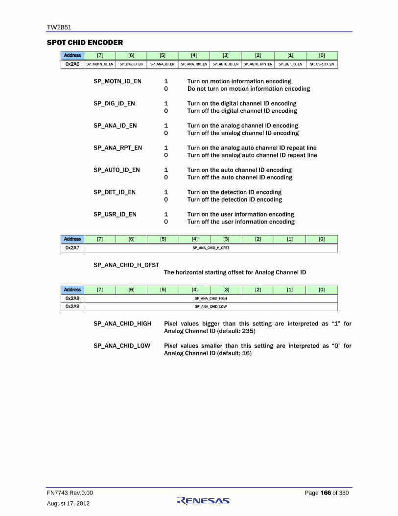
TW2851
FN7743 Rev.0.00 Page 166 of 380
August 17, 2012
SPOT CHID ENCODER
Address [7] [6] [5] [4] [3] [2] [1] [0]
0x2A6 SP_MOTN_ID_EN SP_DIG_ID_EN SP_ANA_ID_EN SP_ANA_RIC_EN SP_AUTO_ID_EN SP_AUTO_RPT_EN SP_DET_ID_EN SP_USR_ID_EN
SP_MOTN_ID_EN 1 Turn on motion information encoding
0 Do not turn on motion information encoding
SP_DIG_ID_EN 1 Turn on the digital channel ID encoding
0 Turn off the digital channel ID encoding
SP_ANA_ID_EN 1 Turn on the analog channel ID encoding
0 Turn off the analog channel ID encoding
SP_ANA_RPT_EN 1 Turn on the analog auto channel ID repeat line
0 Turn off the analog auto channel ID repeat line
SP_AUTO_ID_EN 1 Turn on the auto channel ID encoding
0 Turn off the auto channel ID encoding
SP_DET_ID_EN 1 Turn on the detection ID encoding
0 Turn off the detection ID encoding
SP_USR_ID_EN 1 Turn on the user information encoding
0 Turn off the user information encoding
Address [7] [6] [5] [4] [3] [2] [1] [0]
0x2A7 SP_ANA_CHID_H_OFST
SP_ANA_CHID_H_OFST
The horizontal starting offset for Analog Channel ID
Address [7] [6] [5] [4] [3] [2] [1] [0]
0x2A8 SP_ANA_CHID_HIGH
0x2A9 SP_ANA_CHID_LOW
SP_ANA_CHID_HIGH Pixel values bigger than this setting are interpreted as “1” for
Analog Channel ID (default: 235)
SP_ANA_CHID_LOW Pixel values smaller than this setting are interpreted as “0” for
Analog Channel ID (default: 16)

TW2851
FN7743 Rev.0.00 Page 167 of 380
August 17, 2012
Address [7] [6] [5] [4] [3] [2] [1] [0]
0x2AA SP_CHID_V_OFSTO 0 SP_CHID_V_OFST
0x2AB SP_CHID_V_OFSTE 0 SP_ANA_CHID_BW
SP_CHID_V_OFSTO Control the vertical starting offset on top of SP_CHID_V_OFST in
odd field for Analog Channel ID
SP_CHID_V_OFSTE Control the vertical starting offset on top of SP_CHID_V_OFST in
even field for Analog Channel ID
SP_CHID_V_OFST Vertical starting offset for Analog Channel ID. The actual vertical
line offset is SP_CHID_V_OFST + SP_CHID_V_OFSTO or
SP_CHID_V_OFST + SP_CHID_V_OFSTE
SP_ANA_CHID_BW Control the pixel width of each bit for Analog Channel ID
0 1 pixel
: :
31 32 pixels (default)
Address [7] [6] [5] [4] [3] [2] [1] [0]
0x2AC 0 0 0 0 0 0 0 SP_GEN_EN
SP_GEN_EN Internal Test Function
Default 0
Address [7] [6] [5] [4] [3] [2] [1] [0]
0x2AD SP_CHNUM1 SP_CHNUM0
0x2AE SP_CHNUM3 SP_CHNUM2
SP_CHNUM The Channel Number to display in non-switch mode
SP_CHNUMx[3:2]: CHIP ID
SP_CHNUMx[1:0]: PORT ID

TW2851
FN7743 Rev.0.00 Page 168 of 380
August 17, 2012
Address [7] [6] [5] [4] [3] [2] [1] [0]
0x2B0 SP_USER_CHID[7:0]
0x2B1 SP_USER_CHID[15:8]
0x2B2 SP_USER_CHID[23:16]
0x2B3 SP_USER_CHID[31:24]
0x2B4 SP_USER_CHID[39:32]
0x2B5 SP_USER_CHID[47:40]
0x2B6 SP_USER_CHID[55:48]
0x2B7 SP_USER_CHID[63:56]
SP_USER_CHID Used to set the USER Channel ID for SPOT path.
Address [7] [6] [5] [4] [3] [2] [1] [0]
0x2C0 SP_16
SP_16 16 Window Display Mode
Address [7] [6] [5] [4] [3] [2] [1] [0]
0x2C1 SP_16_WINNUM1 SP_16_WINNUM0
0x2C2 SP_16_WINNUM3 SP_16_WINNUM2
SP_16_WINNUM The window location of the 16 window configuration. The 16
windows are arranged as shown in the following figure.
0 1 2 3
4 5 6 7
8 9 10 11
12 13 14 15
FIGURE 58. THE WINDOW ID OF THE 16 WINDOW CONFIGURATION

TW2851
FN7743 Rev.0.00 Page 169 of 380
August 17, 2012
Display CVBS Processing
DOWN-SCALING
Address [7] [6] [5] [4] [3] [2] [1] [0]
0x1C0 CVBS_SCL_HACTIVE[7:0]
0x1C1 CVBS_SCL_VACTIVE[7:0]
0x1C2 CVBS_SCL_VACTIVE[8] CVBS_SCL_HACTIVE[9:8]
CVBS_SCL_HACTIVE The horizontal active pixel number for display CVBS path
downscaler
CVBS_SCL_VACTIVE The vertical active line number for display CVBS path
downscaler
Address [7] [6] [5] [4] [3] [2] [1] [0]
0x1C3 CVBS_VSCALE[7:0]
0x1C4 CVBS_VSCALE[15:8]
0x1C6 CVBS_HSCALE[7:0]
0x1C7 CVBS_HSCALE[15:8]
CVBS_VSCALE The vertical scaling factor for display CVBS path downscaler.
0x1FFF is scaling factor of 1.
CVBS_VSCALE = Input line number (CVBS_SCL_VACTIVE) * 8191 /
(Output line number + 1)
**Note: line number means the number of lines in a field
CVBS_HSCALE The horizontal factor for display CVBS path downscaler. 0x1FFF
is scaling factor of 1,
CVBS_HSCALE = Input pixel number (CVBS_SCL_HACTIVE) * 8191 /
(Output pixel number + 1)
Address [7] [6] [5] [4] [3] [2] [1] [0]
0x1C5 CVBS_ODD_SKEW CVBS_EVEN_SKEW
CVBS_ODD_SKEW Additional vertical offset on odd fields
CVBS_EVEN_SKEW Additional vertical offset on even fields

TW2851
FN7743 Rev.0.00 Page 170 of 380
August 17, 2012
Address [7] [6] [5] [4] [3] [2] [1] [0]
0x1C8 CVBS_LIM656 CVBS_V_OFST CVBS_VSYNC_POL CVBS_HSYNC_POL CVBS_HSFLT CVBS_VSFLT
CVBS_LIM656 1 Limit the CVBS display pixel outputs (YUV) to between
16 and
235 (Default)
0 Limit the CVBS display pixel outputs (YUV) to between 1
and 254
CVBS_V_OFST 1 Enable using different offset for EVEN/ODD field during
vertical scaling (Default)
0 Use the same offset for EVEN/ODD field during vertical
scaling
CVBS_VSYNC_POL 1 Reverse the VS polarity for CVBS display (Default)
0 Do not reverse the VS polarity for CVBS display
CVBS_HSYNC_POL 1 Reverse the HS polarity for CVBS display (Default)
0 Do not reverse the HS polarity for CVBS display
CVBS_HSFLT Select the CVBS display horizontal downscaler anti-aliasing filter
mode
0 Full bandwidth (Default)
1 2 MHz bandwidth
2 1.5 MHz bandwidth
3 1 MHz bandwidth
CVBS_VSFLT Select the CVBS display vertical downscaler anti-aliasing filter
mode
0 Full bandwidth (Default)
1 0.25 line-rate bandwidth
2,3 0.18 line-rate bandwidth
Address [7] [6] [5] [4] [3] [2] [1] [0]
0x1C9 0 0 0 0 CVBS_FLD_POL CVBS_T_FDLY CVBS_T_VSCL CVBS_T_CPALDLY
CVBS_FLD_POL 1 Reverse the Display CVBS field polarity
0 Do not reverse the field polarity
CVBS_T_FDLY Set display CVBS scaler field delay mode for testing
CVBS_T_VSCL Set display CVBS vertical scaler scaling factor to be 1 for testing
CVBS_T_CPALDLY Set display CVBS scaler chroma delay in PAL mode

TW2851
FN7743 Rev.0.00 Page 171 of 380
August 17, 2012
Address [7] [6] [5] [4] [3] [2] [1] [0]
0x1CA CVBS_TEST CVBS_SOFT_RST CVBS_HSCL_BP CVBS_PALDLY
CVBS_TEST 0001 Enable display CVBS scaler test pattern with data valid
from the pattern generator
0010 Enable display CVBS scaler test pattern with data valid
from the display path
CVBS_SOFT_RST Display CVBS scaler software reset
CVBS_HSCL_BP Bypass display CVBS horizontal scaler
CVBS_PALDLY Set PAL delay mode
Address [7] [6] [5] [4] [3] [2] [1] [0]
0x1CB C_V_START
0x1CC C_V_END [7:0]
0x1CD C_LINE_INS C_V_END[8]
C_V_START Set the starting line number of active video shown in PAL mode
C_V_END Set the end line number of active video shown in PAL mode
C_LINE_INS Enable inserting blanking lines at the beginning and end in PAL
mode
Display VGA / LCD Processing
Address [7] [6] [5] [4] [3] [2] [1] [0]
0x480 VGA_RD_RST VGA_RST
VGA_RST Software Reset for VGA / De-Interlacer / Brightness Control / RGB
control, timing generation modules. When this bit is set, the VGA
sync is lost.
VGA_RD_RST Software Reset of the video buffer read side of the VGA path. When
this bit is set, the VGA output become blanks, and the VGA sync is
not lost. This bit can be set when the display configuration change
is performed.

TW2851
FN7743 Rev.0.00 Page 172 of 380
August 17, 2012
Address [7] [6] [5] [4] [3] [2] [1] [0]
0x4E0 USE_GAMMAB USE_GAMMAG USE_GAMMAR
0x4E1 DITHER_BP S_DM S_BC
USE_GAMMAR Enable red color gamma table
USE_GAMMAG Enable green color gamma table
USE_GAMMAB Enable blue color gamma table
S_BC Output Pixel Width for each of R, G, B value
0: 8:8:8 (default)
1: 6:6:6
2: 5:6:5
3: 5:5:5
4: 4:4:4
5: 3:3:3
6: 3:3:2
S_DM Dithering mode configuration. This specifies the number of lower
bits for dithering.
DITHER_BP Bypass dithering
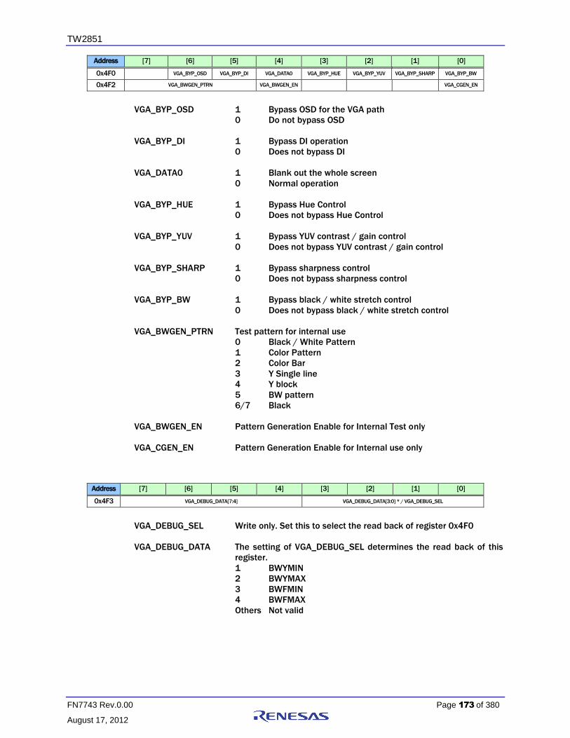
TW2851
FN7743 Rev.0.00 Page 173 of 380
August 17, 2012
Address [7] [6] [5] [4] [3] [2] [1] [0]
0x4F0 VGA_BYP_OSD VGA_BYP_DI VGA_DATA0 VGA_BYP_HUE VGA_BYP_YUV VGA_BYP_SHARP VGA_BYP_BW
0x4F2 VGA_BWGEN_PTRN VGA_BWGEN_EN VGA_CGEN_EN
VGA_BYP_OSD 1 Bypass OSD for the VGA path
0 Do not bypass OSD
VGA_BYP_DI 1 Bypass DI operation
0 Does not bypass DI
VGA_DATA0 1 Blank out the whole screen
0 Normal operation
VGA_BYP_HUE 1 Bypass Hue Control
0 Does not bypass Hue Control
VGA_BYP_YUV 1 Bypass YUV contrast / gain control
0 Does not bypass YUV contrast / gain control
VGA_BYP_SHARP 1 Bypass sharpness control
0 Does not bypass sharpness control
VGA_BYP_BW 1 Bypass black / white stretch control
0 Does not bypass black / white stretch control
VGA_BWGEN_PTRN Test pattern for internal use
0 Black / White Pattern
1 Color Pattern
2 Color Bar
3 Y Single line
4 Y block
5 BW pattern
6/7 Black
VGA_BWGEN_EN Pattern Generation Enable for Internal Test only
VGA_CGEN_EN Pattern Generation Enable for Internal use only
Address [7] [6] [5] [4] [3] [2] [1] [0]
0x4F3 VGA_DEBUG_DATA[7:4] VGA_DEBUG_DATA[3:0] * / VGA_DEBUG_SEL
VGA_DEBUG_SEL Write only. Set this to select the read back of register 0x4F0
VGA_DEBUG_DATA The setting of VGA_DEBUG_SEL determines the read back of this
register.
1 BWYMIN
2 BWYMAX
3 BWFMIN
4 BWFMAX
Others Not valid

TW2851
FN7743 Rev.0.00 Page 174 of 380
August 17, 2012
UP-SCALING
Address [7] [6] [5] [4] [3] [2] [1] [0]
0x4A0 UPS_BG_COLR
UPS_BG_COLR Background color used for UPS
Y = {UPS_BG_COLR[7:6], 6’b0}
Cb = {UPS_BG_COLR[5:3], 5’b0}
Cr = {UPS_BG_COLR[2:0], 5’b0}
Address [7] [6] [5] [4] [3] [2] [1] [0]
0x4A1 UPS_HST
0x4A2 UPS_VST
0x4A3 UPS_HACTIVE_O[7:0]
0x4A4 UPS_VACTIVE_O[7:0]
0x4A5 UPS_VACTIVE_O[10:8] UPS_HACTIVE_O[10:8]
UPS_HST Specify the video starting horizontal location in the output video
frame
UPS_VST Specify the video starting vertical location in the output video
frame
UPS_HACTIVE_O Specify the video width shown in the output video frame after
scaling
UPS_VACTIVE_O Specify the video height shown in the output video frame after
scaling
Address [7] [6] [5] [4] [3] [2] [1] [0]
0x4A8 UPS_HACTIVE_IN[7:0]
0x4A9 UPS_VACTIVE_IN[7:0]
0x4AA UPS_VACTIVE_IN[10:8] UPS_HACTIVE_IN[10:8]
UPS_HACTIVE_IN Specify the upscaler input horizontal video width
UPS_VACTIVE_IN Specify the upscaler input vertical video height
Address [7] [6] [5] [4] [3] [2] [1] [0]
0x4AB UPS_HSCALE[7:0]
0x4AC UPS_HSCALE[12:0]
0x4AD UPS_VSCALE[7:0]
0x4AE UPS_VSCALE[10:8]
UPS_HSCALE Horizontal scaling factor. 0x1000 represents scaling factor of 1
UPS_VSCALE Vertical scaling factor. 0x400 represents scaling factor of 1

TW2851
FN7743 Rev.0.00 Page 175 of 380
August 17, 2012
Address [7] [6] [5] [4] [3] [2] [1] [0]
0x4AF VGA_BLACKOPUT
VGA_BLACKOUT 1 Black out the VGA output
0 Normal display
GAMMA TABLE
Address [7] [6] [5] [4] [3] [2] [1] [0]
0x488 GAMMA_ADDR[7:0]
0x489 GAMMA_ADDR[9:8]
0x48A GAMMA_WDATA[7:0]
0x48B GAMMA_WDATA[9:8]
0x48C GAMMA_RDATA[7:0]*
0x48D GAMMA_RDATA[9:8]*
0x48E GAMMA_RD_START
GAMMA_ADDR Gamma table address
GAMMA_WDATA Gamma table write data. The indirect write starts after writing
0x48B
GAMMA_RDATA Gamma table read data (Read Only)
GAMMA_RD_START Command to start a read by writing register 0x48E. Data written to
0x48E does not matter.
2D DE-INTERLACE
Address [7] [6] [5] [4] [3] [2] [1] [0]
0x490 M2DI_LOW_ANGLE_CNTL M2DI_USE_BOB
M2DI_LOW_ANGLE_CNTL
Disable a specific criterion to disqualify low angle. Default 0
M2DI_USE_BOB Use BOB instead of low angle. Default 0
Address [7] [6] [5] [4] [3] [2] [1] [0]
0x491 0 0 0 1 1 0 0 1
0x492 0 0 1 1 1 1 0 0
0x493 1 1 0 0 1 0 0 0
0x494 1 0 1 1 0 1 0 0
0x495 0 0 0 0 0 0 0 1
0x496 0 0 0 0 1 0 1 0
0x497 0 0 0 0 1 0 1 0
Reserved

TW2851
FN7743 Rev.0.00 Page 176 of 380
August 17, 2012
Address [7] [6] [5] [4] [3] [2] [1] [0]
0x498 M2DI_FRM_WIDTH[7:0]
0x499 M2DI_FRM_PITCH[7:0]
0x49A M2DI_FRM_PITCH[10:8] M2DI_FRM_WIDTH[10:8]
0x49B M2DI_FRM_HEIGHT[7:0]
0x49C M2DI_FRM_HEIGHT[9:8]
M2DI_FRM_WIDTH The frame width of the incoming video in pixels
M2DI_FRM_PITCH The frame width allocated in the memory including the unused
portion at the end of each line
M2DI_FRM_HEIGHT The frame height of the incoming video in lines
IMAGE ENHANCEMENT
Address [7] [6] [5] [4] [3] [2] [1] [0]
0x4B0 VGA_SHWIN VGA_SHCOR
0x4B1 VGA_OVERSHOOT VGA_SHARP
VGA_SHWIN[1] Sharpening filter window size selection
0 2 pixels
1 4 pixels
VGA_SHWIN[0] Sharpening filter min/max window size selection
0 2 pixels
1 4 pixels
VGA_SHCOR Sharpening Coring Setting
VGA_OVERSHOOT Sharpening overshoot setting
VGA_SHARP Sharpening gain
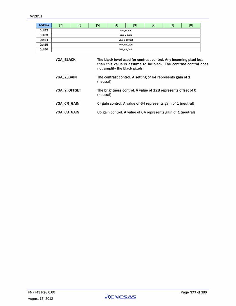
TW2851
FN7743 Rev.0.00 Page 177 of 380
August 17, 2012
Address [7] [6] [5] [4] [3] [2] [1] [0]
0x4B2 VGA_BLACK
0x4B3 VGA_Y_GAIN
0x4B4 VGA_Y_OFFSET
0x4B5 VGA_CR_GAIN
0x4B6 VGA_CB_GAIN
VGA_BLACK The black level used for contrast control. Any incoming pixel less
than this value is assume to be black. The contrast control does
not amplify the black pixels.
VGA_Y_GAIN The contrast control. A setting of 64 represents gain of 1
(neutral)
VGA_Y_OFFSET The brightness control. A value of 128 represents offset of 0
(neutral)
VGA_CR_GAIN Cr gain control. A value of 64 represents gain of 1 (neutral)
VGA_CB_GAIN Cb gain control. A value of 64 represents gain of 1 (neutral)

TW2851
FN7743 Rev.0.00 Page 178 of 380
August 17, 2012
Address [7] [6] [5] [4] [3] [2] [1] [0]
0x4B7 VGA_BLKLVL VGA_WHTLVL VGA_HUEADJ
0x4B8 VGA_BWLST[7:0]
0x4B9 VGA_BWLEND[7:0]
0x4BA VGA_BWLEND[11:8] VGA_BWLST[11:8]
0x4BB VGA_BWFGAIN VGA_BWHGAIN
0x4BC VGA_BTILT
0x4BD VGA_WTILT
0x4BE VGA_BLIMIT
0x4BF VGA_WLIMIT
VGA_HUEADJ HUE Control
VGA_WHTLVL 0 235 as white
1 255 as white
VGA_BLKLVL 0 0 as black
1 16 as black
VGA_BWLST The first line of the black / white detection window for BW stretch
VGA_BWLEND The last line of the black / white detection window for BW stretch
VGA_BWHGAIN Tap for pixel recursive filtering before black / white line minmax
detection
VGA_BWFGAIN Tap for field recursive filtering before black / white field minmax
detection
VGA_BTILT Black Tilt point for BW stretch
VGA_WTILT White Tilt point for BW stretch
VGA_BLIMIT The darkest pixel value after BW stretch
VGA_WLIMIT The brightest pixel value after BW stretch
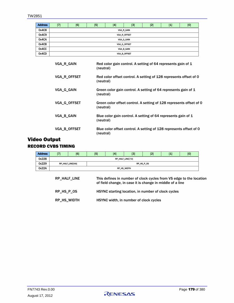
TW2851
FN7743 Rev.0.00 Page 179 of 380
August 17, 2012
Address [7] [6] [5] [4] [3] [2] [1] [0]
0x4C8 VGA_R_GAIN
0x4C9 VGA_R_OFFSET
0x4CA VGA_G_GAIN
0x4CB VGA_G_OFFSET
0x4CC VGA_B_GAIN
0x4CD VGA_B_OFFSET
VGA_R_GAIN Red color gain control. A setting of 64 represents gain of 1
(neutral)
VGA_R_OFFSET Red color offset control. A setting of 128 represents offset of 0
(neutral)
VGA_G_GAIN Green color gain control. A setting of 64 represents gain of 1
(neutral)
VGA_G_OFFSET Green color offset control. A setting of 128 represents offset of 0
(neutral)
VGA_B_GAIN Blue color gain control. A setting of 64 represents gain of 1
(neutral)
VGA_B_OFFSET Blue color offset control. A setting of 128 represents offset of 0
(neutral)
Video Output
RECORD CVBS TIMING
Address [7] [6] [5] [4] [3] [2] [1] [0]
0x228 RP_HALF_LINE[7:0]
0x229 RP_HALF_LINE[9:8] RP_HS_P_OS
0x22A RP_HS_WIDTH
RP_HALF_LINE This defines in number of clock cycles from VS edge to the location
of field change, in case it is change in middle of a line
RP_HS_P_OS HSYNC starting location, in number of clock cycles
RP_HS_WIDTH HSYNC width, in number of clock cycles

TW2851
FN7743 Rev.0.00 Page 180 of 380
August 17, 2012
Address [7] [6] [5] [4] [3] [2] [1] [0]
0x22B RP_TOP_VS_END
0x22C RP_BOT_VS_END
0x22D RP_T_VS_POS RP_TOP_VS_OS
0x22E RP_B_VS_PS RP_BOT_VS_OS
RP_TOP_VS_END VSYNC trailing edge location of top field, in number of lines
RP_BOT_VS_END VSYNC trailing edge location of bottom field, in number of lines
RP_TOP_VS_OS VSYNC leading edge location of top field, in number of lines
RP_BOT_VS_OS VSYNC leading edge location of bottom field, in number of lines
RP_T_VS_POS Enable the top field vsync edge at the middle of a line
RP_B_VS_POS Enable the bottom field vsync edge at the middle of a line
Address [7] [6] [5] [4] [3] [2] [1] [0]
0x22F RP_HS_POL RP_VS_POL RP_FLD_POL RP_VAV_POL RP_HAV_POL RP_ 656_ERRCHK
RP_HS_POL Output HSYNC polarity control
RP_VS_POL Output VSYNC polarity control
RP_FLD_POL Output FIELD polarity control
RP_VAV_POL Output VAV polarity control
RP_HAV_POL Output HAV polarity control
RP_656_ERRCHK Enable 656 SAV/EAV error check
SPOT CVBS TIMING
Address [7] [6] [5] [4] [3] [2] [1] [0]
0x2B8 SP_HALF_LINE[7:0]
0x2B9 SP_HALF_LINE[9:8] SP_HS_P_OS
0x2BA SP_HS_WIDTH
SP_HALF_LINE This defines in number of clock cycles from VS edge to the location
of field change, in case it is change in middle of a line
SP_HS_P_OS HSYNC starting location, in number of clock cycles
SP_HS_WIDTH HSYNC width, in number of clock cycles
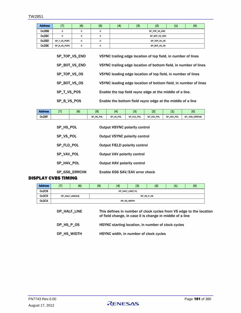
TW2851
FN7743 Rev.0.00 Page 181 of 380
August 17, 2012
Address [7] [6] [5] [4] [3] [2] [1] [0]
0x2BB 0 0 0 SP_TOP_VS_END
0x2BC 0 0 0 SP_BOT_VS_END
0x2BD SP_T_VS_POFS 0 0 SP_TOP_VS_OS
0x2BE SP_B_VS_POFS 0 0 SP_BOT_VS_OS
SP_TOP_VS_END VSYNC trailing edge location of top field, in number of lines
SP_BOT_VS_END VSYNC trailing edge location of bottom field, in number of lines
SP_TOP_VS_OS VSYNC leading edge location of top field, in number of lines
SP_BOT_VS_OS VSYNC leading edge location of bottom field, in number of lines
SP_T_VS_POS Enable the top field vsync edge at the middle of a line.
SP_B_VS_POS Enable the bottom field vsync edge at the middle of a line
Address [7] [6] [5] [4] [3] [2] [1] [0]
0x2BF SP_HS_POL SP_VS_POL SP_FLD_POL SP_VAV_POL SP_HAV_POL SP_ 656_ERRCHK
SP_HS_POL Output HSYNC polarity control
SP_VS_POL Output VSYNC polarity control
SP_FLD_POL Output FIELD polarity control
SP_VAV_POL Output VAV polarity control
SP_HAV_POL Output HAV polarity control
SP_656_ERRCHK Enable 656 SAV/EAV error check
DISPLAY CVBS TIMING
Address [7] [6] [5] [4] [3] [2] [1] [0]
0x2C8 DP_HALF_LINE[7:0]
0x2C9 DP_HALF_LINE[9:8] DP_HS_P_OS
0x2CA DP_HS_WIDTH
DP_HALF_LINE This defines in number of clock cycles from VS edge to the location
of field change, in case it is change in middle of a line
DP_HS_P_OS HSYNC starting location, in number of clock cycles
DP_HS_WIDTH HSYNC width, in number of clock cycles
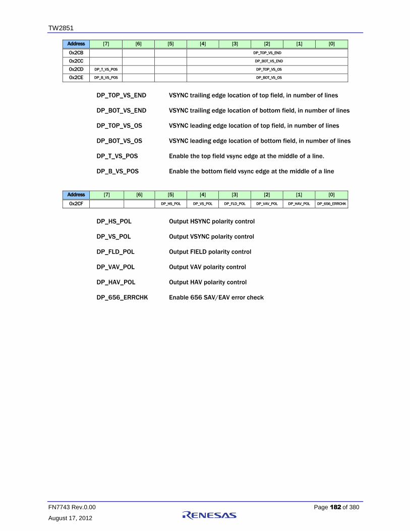
TW2851
FN7743 Rev.0.00 Page 182 of 380
August 17, 2012
Address [7] [6] [5] [4] [3] [2] [1] [0]
0x2CB DP_TOP_VS_END
0x2CC DP_BOT_VS_END
0x2CD DP_T_VS_POS DP_TOP_VS_OS
0x2CE DP_B_VS_POS DP_BOT_VS_OS
DP_TOP_VS_END VSYNC trailing edge location of top field, in number of lines
DP_BOT_VS_END VSYNC trailing edge location of bottom field, in number of lines
DP_TOP_VS_OS VSYNC leading edge location of top field, in number of lines
DP_BOT_VS_OS VSYNC leading edge location of bottom field, in number of lines
DP_T_VS_POS Enable the top field vsync edge at the middle of a line.
DP_B_VS_POS Enable the bottom field vsync edge at the middle of a line
Address [7] [6] [5] [4] [3] [2] [1] [0]
0x2CF DP_HS_POL DP_VS_POL DP_FLD_POL DP_VAV_POL DP_HAV_POL DP_656_ERRCHK
DP_HS_POL Output HSYNC polarity control
DP_VS_POL Output VSYNC polarity control
DP_FLD_POL Output FIELD polarity control
DP_VAV_POL Output VAV polarity control
DP_HAV_POL Output HAV polarity control
DP_656_ERRCHK Enable 656 SAV/EAV error check

TW2851
FN7743 Rev.0.00 Page 183 of 380
August 17, 2012
CVBS ENCODER CONTROL
Address [7] [6] [5] [4] [3] [2] [1] [0]
0x2D0 VE_FSCSEL 0 VE_FLD VE_VS 0 1 VE_PAL_NTSC
VE_FSCSEL Set the sub-carrier frequency for video encoder
0 3.57954545 MHz (default)
1 4.43361875 MHz
2 3.57561149 MHz
3 3.58205625 MHz
VE_FLD Define the field detection type
0 Use field from input field signal (default)
1 Detect field from combination of HSENC and VSENC
signals
VE_VS Define the vertical sync (VSYNC) detection type
0 Use signal from input VSYNC
1 Detect VSYNC from combination of HSENC and FLDEN
VE_PAL_NTSC Define the PAL or NTSC
0 NTSC
1 PAL
Address [7] [6] [5] [4] [3] [2] [1] [0]
0x2D1 VE_HSDEL[9:8] VE_FLDPOL VE_VSPOL VE_HSPOL VE_PED VE_FDRST VE_PHALT
VE_FLDPOL Control the field polarity
0 Even field is high (default)
1 Odd field is high
VE_VSPOL Control the vertical sync polarity
0 Active low (default)
1 Active high
VE_HSPOL Control the horizontal sync polarity
0 Active low (default)
1 Active high
VE_PED Set 7.5 IRE for pedestal level
0 IRE for pedestal level
1 7.5 IRE for pedestal level (default)
VE_FDRST Reset the phase alternation every 8 field
0 No reset mode (default)
1 Reset the phase alternation every 8 field
VE_PHALT Set the phase alternation
0 Disable phase alternation for line-by-line (default)
1 Enable phase alternation for line-by-line

TW2851
FN7743 Rev.0.00 Page 184 of 380
August 17, 2012
Address [7] [6] [5] [4] [3] [2] [1] [0]
0x2D1 VE_HSDEL[9:8] VE_FLDPOL VE_VSPOL VE_HSPOL VE_PED VE_FDRST VE_PHALT
0x2D2 VE_HSDEL[7:0]
0x2D3 VE_VSOFF VE_VSDEL
VE_HSDEL Control the pixel delay of horizontal sync from active video by ½
pixels/Step
0 No delay
: :
256 64 pixels delay (default)
: :
1023 255 pixels delay
VE_VSDEL Control the line delay of vertical sync from active video by 1
line/step
0 No delay
: :
32 32 lines delay (default)
: :
63 63 lines delay
VE_VSOFF Compensate the field offset for the first active video line
0 Apply same VE_VSDEL for odd and even field (default)
1 Apply (VE_VSDEL+1) for odd and VE_VSDEL for even
field
2 Apply VE_VSDEL for odd and (VE_VSDEL + 1) for even
field
3 Apply VE_VSDEL for odd and (VE_VSDEL+2) for even
field
Address [7] [6] [5] [4] [3] [2] [1] [0]
0x2D4 VE_ACTIVE_VDEL
0x2D5 VE_ACTIVE_HDEL
VE_ACTIVE_VDEL Control the line delay of active video by 1 line/step
0 -12 lines delay
: :
12 0 line delay (default)
: :
25 13 lines delay
VE_ACTIVE_HDEL Control the pixel delay of active video by 1 pixel/step
0 -32 pixels delay
: :
32 0 pixel delay
: :
63 31 pixels delay
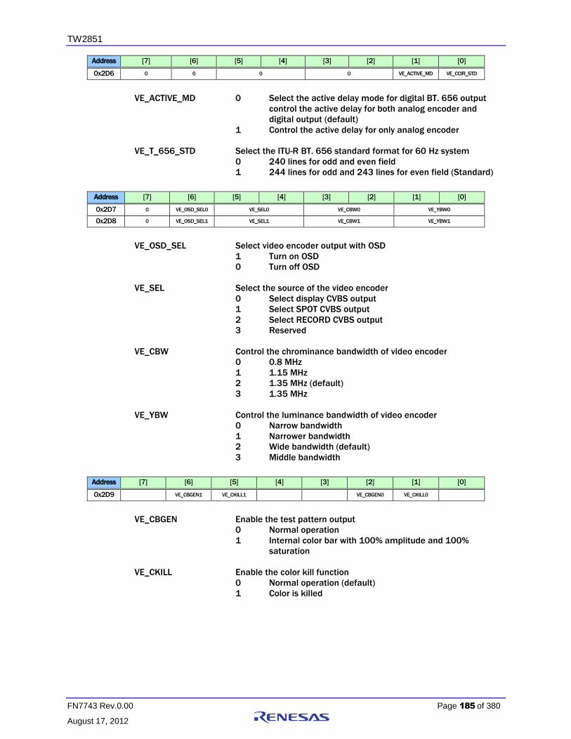
TW2851
FN7743 Rev.0.00 Page 185 of 380
August 17, 2012
Address [7] [6] [5] [4] [3] [2] [1] [0]
0x2D6 0 0 0 0 VE_ACTIVE_MD VE_CCIR_STD
VE_ACTIVE_MD 0 Select the active delay mode for digital BT. 656 output
control the active delay for both analog encoder and
digital output (default)
1 Control the active delay for only analog encoder
VE_T_656_STD Select the ITU-R BT. 656 standard format for 60 Hz system
0 240 lines for odd and even field
1 244 lines for odd and 243 lines for even field (Standard)
Address [7] [6] [5] [4] [3] [2] [1] [0]
0x2D7 0 VE_OSD_SEL0 VE_SEL0 VE_CBW0 VE_YBW0
0x2D8 0 VE_OSD_SEL1 VE_SEL1 VE_CBW1 VE_YBW1
VE_OSD_SEL Select video encoder output with OSD
1 Turn on OSD
0 Turn off OSD
VE_SEL Select the source of the video encoder
0 Select display CVBS output
1 Select SPOT CVBS output
2 Select RECORD CVBS output
3 Reserved
VE_CBW Control the chrominance bandwidth of video encoder
0 0.8 MHz
1 1.15 MHz
2 1.35 MHz (default)
3 1.35 MHz
VE_YBW Control the luminance bandwidth of video encoder
0 Narrow bandwidth
1 Narrower bandwidth
2 Wide bandwidth (default)
3 Middle bandwidth
Address [7] [6] [5] [4] [3] [2] [1] [0]
0x2D9 VE_CBGEN1 VE_CKILL1 VE_CBGEN0 VE_CKILL0
VE_CBGEN Enable the test pattern output
0 Normal operation
1 Internal color bar with 100% amplitude and 100%
saturation
VE_CKILL Enable the color kill function
0 Normal operation (default)
1 Color is killed

TW2851
FN7743 Rev.0.00 Page 186 of 380
August 17, 2012
DISPLAY CASCADE TIMING
Address [7] [6] [5] [4] [3] [2] [1] [0]
0x508 VDOX_BT1120_SEL VDOX_FLD_POL VDOX_1120_CROP VDOX_HVS_MD VDOX_DIG_OSD_BP DISP_CVBS_EN
DISP_CVBS_EN 1 Enable Display CVBS Path
0 Enable display digital output (either BT1120 or 8-bit
cascade)
VDOX_DIG_OSD_BP 1 Bypass the digital display path OSD
0 Enable the OSD on the display digital output
VDOX_HVS_MD 1 Output HAV/VAV signal at the HSYNC VSYNC port
0 Output regular HSYNC/VSYNC signal
VDOX_1120_CROP 1 BT1120 mode crop window enabled
0 BT1120 mode crop window disabled
VDOX_FLD_POL 1 Reverse the field polarity for display digital
output
0 Do not reverse the field polarity for display digital output
VDOX_BT1120_SEL 1 Select display digital output as the BT1120 output
0 Select display digital output as the 8-bit Cascade output
Address [7] [6] [5] [4] [3] [2] [1] [0]
0x509 VDOX_BT1120_TOP_OS[7:0]
0x50A VDOX_BT1120_BOT_OS[7:0]
0x50B VDOX_BT1120_L_OS[7:0]
0x50C VDOX_BT1120_R_OS[7:0]
0x50D VDOX_BT1120_R_OS[8] VDOX_BT1120_BOT_OS[8]
VDOX_BT1120_TOP_OS Top offset defining the vertical starting location
of active video in the BT1120 (1920x1080) frame
VDOX_BT1120_BOT_OS Bottom offset defining the vertical ending location of
active video in the BT1120 (1920x1080) frame
VDOX_BT1120_L_OS Left offset defining the horizontal starting location of
active video in the BT1120 (1920x1080) frame
VDOXD_BT1120_R_OS Right offset defining the horizontal ending location of
active video in the BT1120 (1920x1080) frame

TW2851
FN7743 Rev.0.00 Page 187 of 380
August 17, 2012
Address [7] [6] [5] [4] [3] [2] [1] [0]
0x50F VDOX_VAV_ODD_OFS
0x510 VDOX_VAV_EVEN_OFS
VDOX_VAV_ODD_OFS The line number between the beginning of the ODD field
and the beginning of VAV of display digital output
(BT1120 or cascade)
VDOX_VAV_EVEN_OFS The line number between the beginning of the EVEN field and the
beginning of VAV of display digital output (BT1120 or
cascade)
Address [7] [6] [5] [4] [3] [2] [1] [0]
0x511 VDOX_VS_POL VDOX_HS_POL VDOX_VS_ETP_EN VDOX_VS_ELP_EN VDOX_VS_OTP_EN VDOX_VS_OLP_EN
VDOX_VS_POL Select the VS polarity of display digital output.
1 Low active
0 High active
VDOX_HS_POL Select the HS polarity of display digital output
1 Low active
0 High active
VDOX_VS_ETP_EN Enable the pixel offset of even field VS trailing edge relative to HS
specified with VDOX_VS_POFS
VDOX_VS_ELP_EN Enable the pixel offset of even field VS leading edge relative to HS
specified with VDOX_VS_POFS
VDOX_VS_OTP_EN Enable the pixel offset of odd field VS trailing edge relative to HS
specified with VDOX_VS_POFS
VDOX_VS_OLP_EN Enable the pixel offset of odd field VS leading edge relative to HS
specified with VDOX_VS_POFS
Address [7] [6] [5] [4] [3] [2] [1] [0]
0x512 VDOX_VS_POFS[11:8] VDOX_VSYNC_WIDTH
0x513 VDOX_VS_POFS[7:0]
VDOX_VS_POFS The pixel offset of VS edge relative to HS for the display digital
output timing
VDOX_VSYNC_WIDTH The VSYNC width in unit of lines for the display digital output
timing
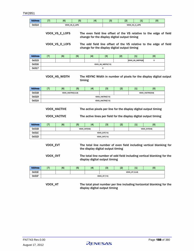
TW2851
FN7743 Rev.0.00 Page 188 of 380
August 17, 2012
Address [7] [6] [5] [4] [3] [2] [1] [0]
0x514 VDOX_VS_E_LOFS VDOX_VS_O_LOFS
VDOX_VS_E_LOFS The even field line offset of the VS relative to the edge of field
change for the display digital output timing
VDOX_VS_O_LOFS The odd field line offset of the VS relative to the edge of field
change for the display digital output timing
Address [7] [6] [5] [4] [3] [2] [1] [0]
0x515 VDOX_HS_WIDTH[8] 0
0x516 VDOX_HS_WIDTH[7:0]
0x517 0
VDOX_HS_WIDTH The HSYNC Width in number of pixels for the display digital output
timing
Address [7] [6] [5] [4] [3] [2] [1] [0]
0x518 VDOX_HACTIVE[11:8] VDOX_VACTIVE[9:8]
0x519 VDOX_VACTIVE[7:0]
0x51A VDOX_HACTIVE[7:0]
VDOX_HACTIVE The active pixels per line for the display digital output timing
VDOX_VACTIVE The active lines per field for the display digital output timing
Address [7] [6] [5] [4] [3] [2] [1] [0]
0x51B VDOX_OVT[9:8] VDOX_EVT[9:8]
0x51C VDOX_EVT[7:0]
0x51D VDOX_OVT[7:0]
VDOX_EVT The total line number of even field including vertical blanking for
the display digital output timing
VDOX_OVT The total line number of odd field including vertical blanking for the
display digital output timing
Address [7] [6] [5] [4] [3] [2] [1] [0]
0x51E VDOX_HT [11:8]
0x51F VDOX_HT [7:0]
VDOX_HT The total pixel number per line including horizontal blanking for the
display digital output timing
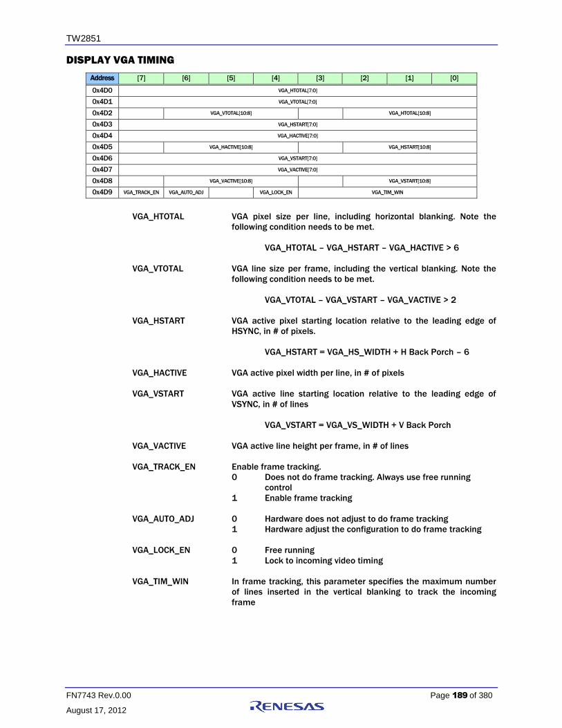
TW2851
FN7743 Rev.0.00 Page 189 of 380
August 17, 2012
DISPLAY VGA TIMING
Address [7] [6] [5] [4] [3] [2] [1] [0]
0x4D0 VGA_HTOTAL[7:0]
0x4D1 VGA_VTOTAL[7:0]
0x4D2 VGA_VTOTAL[10:8] VGA_HTOTAL[10:8]
0x4D3 VGA_HSTART[7:0]
0x4D4 VGA_HACTIVE[7:0]
0x4D5 VGA_HACTIVE[10:8] VGA_HSTART[10:8]
0x4D6 VGA_VSTART[7:0]
0x4D7 VGA_VACTIVE[7:0]
0x4D8 VGA_VACTIVE[10:8] VGA_VSTART[10:8]
0x4D9 VGA_TRACK_EN VGA_AUTO_ADJ VGA_LOCK_EN VGA_TIM_WIN
VGA_HTOTAL VGA pixel size per line, including horizontal blanking. Note the
following condition needs to be met.
VGA_HTOTAL – VGA_HSTART – VGA_HACTIVE > 6
VGA_VTOTAL VGA line size per frame, including the vertical blanking. Note the
following condition needs to be met.
VGA_VTOTAL – VGA_VSTART – VGA_VACTIVE > 2
VGA_HSTART VGA active pixel starting location relative to the leading edge of
HSYNC, in # of pixels.
VGA_HSTART = VGA_HS_WIDTH + H Back Porch – 6
VGA_HACTIVE VGA active pixel width per line, in # of pixels
VGA_VSTART VGA active line starting location relative to the leading edge of
VSYNC, in # of lines
VGA_VSTART = VGA_VS_WIDTH + V Back Porch
VGA_VACTIVE VGA active line height per frame, in # of lines
VGA_TRACK_EN Enable frame tracking.
0 Does not do frame tracking. Always use free running
control
1 Enable frame tracking
VGA_AUTO_ADJ 0 Hardware does not adjust to do frame tracking
1 Hardware adjust the configuration to do frame tracking
VGA_LOCK_EN 0 Free running
1 Lock to incoming video timing
VGA_TIM_WIN In frame tracking, this parameter specifies the maximum number
of lines inserted in the vertical blanking to track the incoming
frame

TW2851
FN7743 Rev.0.00 Page 190 of 380
August 17, 2012
Address [7] [6] [5] [4] [3] [2] [1] [0]
0x4DA VGA_HS_POL VGA_VS_POL
0x4DB VGA_HS_WIDTH
0x4DC VGA_VS_WIDTH
VGA_VS_POL 1 Negative (Low active)
0 Positive (High active)
VGA_HS_POL 1 Negative (Low active)
0 Positive (High active)
VGA_HS_WIDTH VGA HSYNC width in # of pixels
VGA_VS_WIDTH VGA VSYNC height in # of lines
TFT PANEL CONTROL
Address [7] [6] [5] [4] [3] [2] [1] [0]
0x4E2 FP_PX_MODE FP_DE_AH FP_HS_AH FP_VS_AH FP_CK_AH
0x4E3 FP_SEL_LG FP_SIG_OFF FP_CKTPS
FP_PX_MODE 1 Set dual channel LVDS output
0 Set single channel LVDS output
FP_DE_AH 1 Panel DE signal active high
0 Panel DE signal active low
FP_HS_AH 1 Panel HS signal active high
0 Panel HS signal active low
FP_VS_AH 1 Panel VS signal active high
0 Panel VS signal active low
FP_CK_AH Reverse the FPCLK polarity
1 Data is sampled at the falling edge
0 Data is sampled at the rising edge
FP_SEL_LG 0 Select the LVDS mapping of the Samsung type
1 Select the LVDS mapping of the LG type
2 Reserved
3 Reserved
FP_SIG_OFF 0 Do not turn off the panel
1 Turn off the panel
FP_CKTPS Reserved
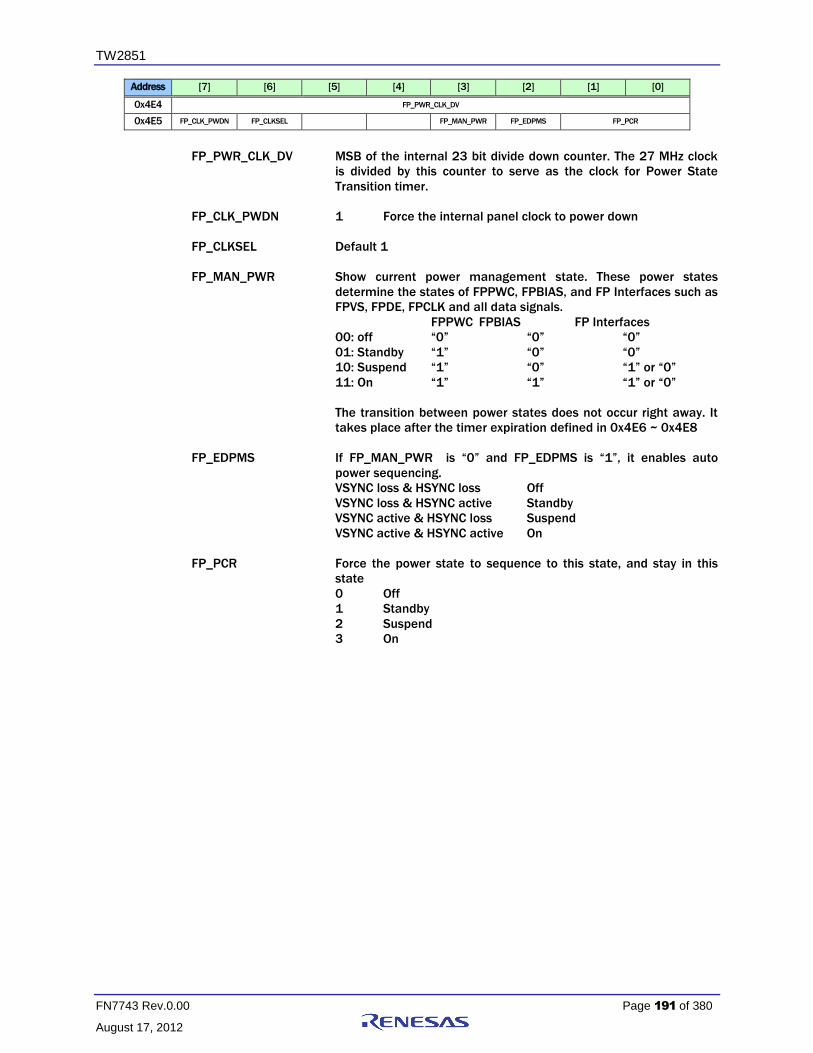
TW2851
FN7743 Rev.0.00 Page 191 of 380
August 17, 2012
Address [7] [6] [5] [4] [3] [2] [1] [0]
0x4E4 FP_PWR_CLK_DV
0x4E5 FP_CLK_PWDN FP_CLKSEL FP_MAN_PWR FP_EDPMS FP_PCR
FP_PWR_CLK_DV MSB of the internal 23 bit divide down counter. The 27 MHz clock
is divided by this counter to serve as the clock for Power State
Transition timer.
FP_CLK_PWDN 1 Force the internal panel clock to power down
FP_CLKSEL Default 1
FP_MAN_PWR Show current power management state. These power states
determine the states of FPPWC, FPBIAS, and FP Interfaces such as
FPVS, FPDE, FPCLK and all data signals.
FPPWC FPBIAS FP Interfaces
00: off “0” “0” “0”
01: Standby “1” “0” “0”
10: Suspend “1” “0” “1” or “0”
11: On “1” “1” “1” or “0”
The transition between power states does not occur right away. It
takes place after the timer expiration defined in 0x4E6 ~ 0x4E8
FP_EDPMS If FP_MAN_PWR is “0” and FP_EDPMS is “1”, it enables auto
power sequencing.
VSYNC loss & HSYNC loss Off
VSYNC loss & HSYNC active Standby
VSYNC active & HSYNC loss Suspend
VSYNC active & HSYNC active On
FP_PCR Force the power state to sequence to this state, and stay in this
state
0 Off
1 Standby
2 Suspend
3 On

TW2851
FN7743 Rev.0.00 Page 192 of 380
August 17, 2012
Address [7] [6] [5] [4] [3] [2] [1] [0]
0x4E6 FP_ITV12 FP_ITV01
0x4E7 FP_ITV32 FP_ITV23
0x4E8 FP_ITV21 FP_ITV10
0x4E9 FP_PWM_CLK_SEL FP_PWM
0x4EB FP_PWM_AL
FP_ITV01 Timer counts for On state to Suspend state transition
FP_ITV12 Timer counts for Suspend state to Standby state transition
FP_ITV23 Timer counts for Standby state to Power Off state
FP_ITV32 Timer counts for Power Off state to Standby state
FP_ITV10 Timer count for Suspend state to On State
FP_ITV21 Timer count for Standby state to Suspend state
FP_PWM_CLK_SEL 1 PWM clock set to 27 MHz
0 PWM clock set to 13.5 MHz
FP_PWM Pulse width of PWM is FP_PWM + 1
FP_PWM_AL PWM Output Polarity
1 Reverse PWM signal output polarity
0 Do not reverse PWM signal output polarity

TW2851
FN7743 Rev.0.00 Page 193 of 380
August 17, 2012
Address [7] [6] [5] [4] [3] [2] [1] [0]
0xE40 LVDS_LP_SEL LVDS_CP_SEL LVDS_EN LVDS_FAB_TEST LVDS_LCD_TEST
0xE41 LVDS_SWAP_CH LVDS_9BIT_DC LVDS_NS_SEL LVDS_DC_BAL LVDS_BITPERPIXEL LVDS_REV_DATA LVDS_SEL_LD
0xE42 LVDS_REV_DCB LVDS_DCB_POL LVDS_MAP_SEL
0xE43 LVDS_VOS_SEL LVDS_I_SEL
LVDS_LP_SEL Default 0
LVDS_CP_SEL Default 0
LVDS_EN 0 LVDS Disabled
1 LVDS Enabled
LVDS_FAB_TEST 0 Normal Operation
1 LVDS Test Mode
LVDS_LCD_TEST 0 Normal Operation
1 LCD Panel Test Mode
LVDS_SWAP_CH 1 Swap LVDS channel 0 and 1
0 Do not swap LVDS channel 0 and 1
LVDS_9BIT_DC 0 Select 7 cycle DC balance, as used in most National
chip
1 Select 9 cycle DC balance, as used in MAXIM chip
LVDS_NS_SEL 0 Output data mapping same as Maxim or THine LVDS
interface protocol
1 Output data mapping same as National interface
protocol
LVDS_DC_BAL 1 DC Balance Enable
0 DC Balance Disable
LVDS_BITPERPIXEL 0 6 bit data output
1 8 bit data output
2 10 bit data output
LVDS_REV_DATA 0 Normal data output format
1 Reverse data output format
LVDS_SEL_LD Load/Shift signal polarity selection
0 Active low
1 Active high
LVDS_REV_DCB 1 Reverse DC balance bit order
LVDS_DCB_POL 1 Reverse DC balance polarity
LVDS_MAP_SEL Change the mapping location of DE, VSYNC and HSYNC signals
000 {DE, VSYNC, HSYNC }
001 {VSYNC, HSYNC, DE }
010 {HSYNC, DE, VSYNC }
100 {DE, HSYNC, VSYNC }
101 {HSYNC, VSYNC, DE }
110 {VSYNC, DE, HSYNC }

TW2851
FN7743 Rev.0.00 Page 194 of 380
August 17, 2012
LVDS_VOS_SEL LVDS Driver Voltage Offset Select
LVDS_I_SEL LVDS Driver Output Swing Select
OSG
OSG BITMAP WRITE / MOVE
Address [7] [6] [5] [4] [3] [2] [1] [0]
0x640 OSG_MEM_WIDTH
OSG_MEM_WIDTH The OSG memory structure width in units of 64 pixels (128 bytes)
Address [7] [6] [5] [4] [3] [2] [1] [0]
0x641 OSG_WRBASE_ADDR
OSG_WRBASE_ADDR
The base address used for writing data into OSG memory
space. This base address can be set statically to treat all the
OSG memory space into a big one, or it can be set
dynamically to match each of the OSG base address at the
write side. The unit is in 64 Kbytes.
The DDR address generated from this register is
{1’b1, OSG_WRBASE_ADDR[7:0], 16’h0}
Address [7] [6] [5] [4] [3] [2] [1] [0]
0x642 0 OSG_COLR_CON 0 1 1 OSG_OPMODE
OSG_COLR_CON 1 Turn on color conversion before writing into the
memory. There is a 4-entry color conversion table
used to match with the pixel value. If it matches,
the pixel is converted to a specified corresponding
output pixel value.
0 Turn off the color conversion function
OSG_OPMODE 0 Bitmap Write Mode – CPU fill all the pixel bitmaps
1 Block Move Mode – Move one block of memory
content from one location to another location
2 Block Fill Mode
3 Reserved
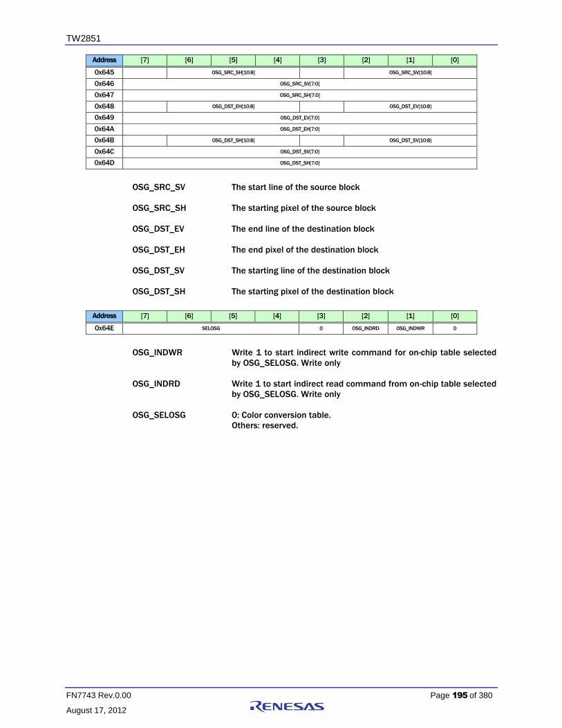
TW2851
FN7743 Rev.0.00 Page 195 of 380
August 17, 2012
Address [7] [6] [5] [4] [3] [2] [1] [0]
0x645 OSG_SRC_SH[10:8] OSG_SRC_SV[10:8]
0x646 OSG_SRC_SV[7:0]
0x647 OSG_SRC_SH[7:0]
0x648 OSG_DST_EH[10:8] OSG_DST_EV[10:8]
0x649 OSG_DST_EV[7:0]
0x64A OSG_DST_EH[7:0]
0x64B OSG_DST_SH[10:8] OSG_DST_SV[10:8]
0x64C OSG_DST_SV[7:0]
0x64D OSG_DST_SH[7:0]
OSG_SRC_SV The start line of the source block
OSG_SRC_SH The starting pixel of the source block
OSG_DST_EV The end line of the destination block
OSG_DST_EH The end pixel of the destination block
OSG_DST_SV The starting line of the destination block
OSG_DST_SH The starting pixel of the destination block
Address [7] [6] [5] [4] [3] [2] [1] [0]
0x64E SELOSG 0 OSG_INDRD OSG_INDWR 0
OSG_INDWR Write 1 to start indirect write command for on-chip table selected
by OSG_SELOSG. Write only
OSG_INDRD Write 1 to start indirect read command from on-chip table selected
by OSG_SELOSG. Write only
OSG_SELOSG 0: Color conversion table.
Others: reserved.

TW2851
FN7743 Rev.0.00 Page 196 of 380
August 17, 2012
Address [7] [6] [5] [4] [3] [2] [1] [0]
0x64F OSG_IDLE OSG_BMWR_BUSY OSG_OP_START
OSG_OP_START Command bit to start the BLOCK MOVE, BLOCK FILL, or BITMAP
WRITE function. Self clear after done.
This bit can be used as status bit for whether the OSG is ready for a
new operation. If it is 0, means the previous operation is done.
Note: do not write 0 to this bit. It may cause unexpected result.
OSG_BMWR_BUSY Read only flag to specify whether the BITMAP WRITE fifo has 256
byte space available to write. If this bit is 0, the MCU can feel free
to write up to 256 bytes without checking this bit again.
OSG_IDLE Read only flag to specify OSG state machine is idle. This bit is
usually the opposite of the OSG_OP_START (0x64F[0]), unless
OSG_OP_START was set at incorrect time during OSG_IDLE is not
1.
0 OSG operation is in progress
1 OSG operation is idle
Address [7] [6] [5] [4] [3] [2] [1] [0]
0x650 OSG_IND_ADDR
OSG_IND_ADDR The indirect access address used to access the internal tables.
Address [7] [6] [5] [4] [3] [2] [1] [0]
0x651 OSG_IND_WRDATA
OSG_IND_WRDATA The indirect write data for writing the color table.
Address [7] [6] [5] [4] [3] [2] [1] [0]
0x652 OSG_UP_DATA[15:0] or OSG_UP_DATA[7:0]
OSG_UP_DATA The BITMAP WRITE data register. Note that in the 16-bit data bus
mode, this address is used to write 16 bits, instead of 8 bits.
Address [7] [6] [5] [4] [3] [2] [1] [0]
0x654 OSG_FILL_COLR[7:0] (Y2)
0x655 OSG_FILL_COLR[15:8] (Cr)
0x656 OSG_FILL_COLR[23:16] (Y1)
0x657 OSG_FILL_COLR31:24] (Cb)
OSG_FILL_COLR[31:24] U pixel value for block fill
OSG_FILL_COLR[23:16] Y1 pixel value for block fill
OSG_FILL_COLR[15:8] V pixel value for block fill
OSG_FILL_COLR[7:0] Y2 pixel value for block fill

TW2851
FN7743 Rev.0.00 Page 197 of 380
August 17, 2012
Address [7] [6] [5] [4] [3] [2] [1] [0]
0x658 OSG_RLC_EN OSG_RLC_32B OSG_RLC_CNT
OSG_RLC_EN Enable proprietary hardware RLC decompression while uploading
the bitmap into the OSG buffer. With this feature turned on, the
uploading bitmap from MCU through the host interface is in RLC
compressed format. The RLC compressed result is decompressed
by the hardware automatically. This reduces the bandwidth
consumption on the host interface.
OSG_RLC_32B 1 Use 32 bit data for compression pattern match
0 Use 16 bit data for compression pattern match
OSG_RLC_CNT Indicate how many bits are used for the repetition count.
0 The repetition count is 16 bits
1 – 15 The repetition count is 1 – 15 bits
The proprietary compression format is as follows:
F, D/C, F, D/C, …..
Where F (1 bit): 0 : indicate the following is pixel data
1 : indicate the following is repetition count
D : Pixel Data in either 16 bits or 32 bits, as specified by
OSG_RLC_32B)
C : Repetition count (how many times the D data is repeated. The
number of bits of this repetition count is controlled by the
OSG_RLC_CNT.
Note: count of 0 means 2**N repetition, where N is OSG_RLC_CNT

TW2851
FN7743 Rev.0.00 Page 198 of 380
August 17, 2012
OSD BITMAP READ
0xm21, 0xm30 ~ 0xm3F, 0xm64 ~ 0xm8F are used to control the read side of the 5 OSDs.
m: 5 – Display VGA OSD
m: 6 – Display CVBS OSD
m: 7 – Record 0 OSD
m: 8 – Record 1 OSD
m: 9 – SPOT OSD
Address [7] [6] [5] [4] [3] [2] [1] [0]
0x521
0x621
0x721
0x821
0x921
0 0 OSD_FLD_POL OSD_VSYNC_POL
OSD_FLD_POL The Polarity control for the OSD to interpret the field signal
OSD_VSYNC_POL The polarity control for the OSD to interpret the VS when signal

TW2851
FN7743 Rev.0.00 Page 199 of 380
August 17, 2012
Address [7] [6] [5] [4] [3] [2] [1] [0]
0x530
0x630
0x730
0x830
0x930
OSD_BLINK_EN
0x531
0x631
0x731
9x831
0x931
OSD_TEST OSD_WINSEL[7:0]
OSD_BLINK_EN Enable blinking
OSD_TEST OSD Test pattern. For internal use only
OSD_WINSEL[n] Selects which window to configure. This is used with registers
0xm35,
0xm37 ~ 0xm3F.
0 ~ 7 Sub-windows
8 Main Window
Address [7] [6] [5] [4] [3] [2] [1] [0]
0x532
0x632
0x732
0x832
0x932
OSD_GLOBAL_ALPHA1 (Main Window)
0x533
0x633
0x733
0x833
0x933
OSD_GLOBAL_ALPHA2 (Sub Windows)
OSD_GLOBAL_ALPHA1 The alpha value for main window
OSD_GLOBAL_ALPHA2 The alpha value for all sub-windows

TW2851
FN7743 Rev.0.00 Page 200 of 380
August 17, 2012
Address [7] [6] [5] [4] [3] [2] [1] [0]
0x534
0x634
0x734
0x834
0x934
0 0 OSD_BLEND_OPT OSD_WINSUB_ON OSD_WINMAIN_ON OSD_P_ALPHA OSD_MODE[1] OSD_MODE[0]
OSD_BLEND_OPT Decide whether single window OSD layer on top or multi-window
OSD
layer on top when blending
OSD_WINSUB_ON Turn on sub-window OSD. Each individual sub-window is enabled by
OSD_WIN_EN in 0xm35
OSD_WINMAIN_ON Turn on the main window OSD
OSD_P_ALPHA (reserved)
OSD_MODE[1:0] For VGA OSD(0x534)
00: 422 UYVY format
01: 565 UYV format
11: 565 RGB format
For other OSD (0x634/0x734/0x834/0x934)
Always 422 UYVY format
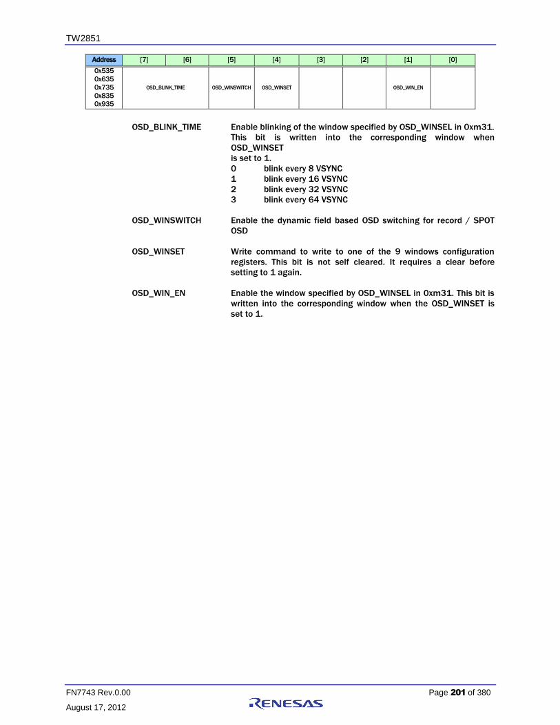
TW2851
FN7743 Rev.0.00 Page 201 of 380
August 17, 2012
Address [7] [6] [5] [4] [3] [2] [1] [0]
0x535
0x635
0x735
0x835
0x935
OSD_BLINK_TIME OSD_WINSWITCH OSD_WINSET OSD_WIN_EN
OSD_BLINK_TIME Enable blinking of the window specified by OSD_WINSEL in 0xm31.
This bit is written into the corresponding window when
OSD_WINSET
is set to 1.
0 blink every 8 VSYNC
1 blink every 16 VSYNC
2 blink every 32 VSYNC
3 blink every 64 VSYNC
OSD_WINSWITCH Enable the dynamic field based OSD switching for record / SPOT
OSD
OSD_WINSET Write command to write to one of the 9 windows configuration
registers. This bit is not self cleared. It requires a clear before
setting to 1 again.
OSD_WIN_EN Enable the window specified by OSD_WINSEL in 0xm31. This bit is
written into the corresponding window when the OSD_WINSET is
set to 1.
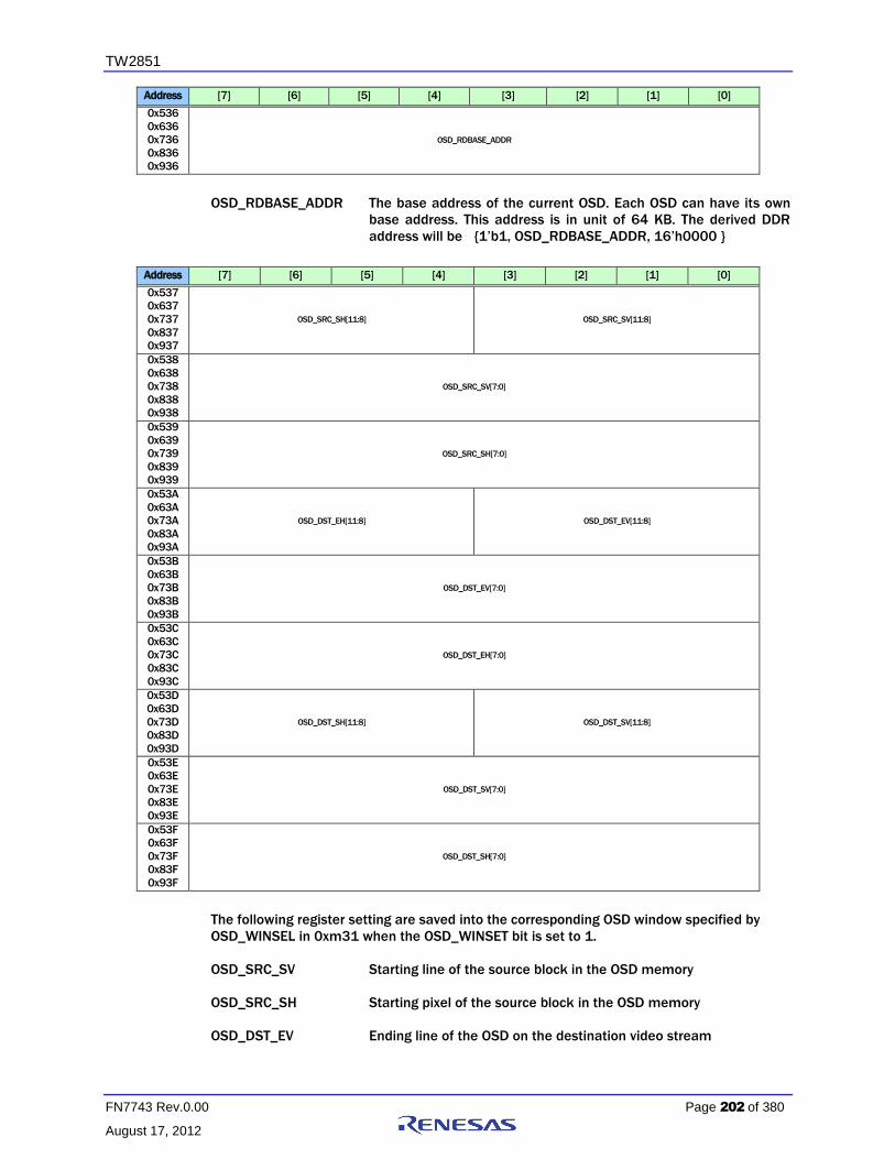
TW2851
FN7743 Rev.0.00 Page 202 of 380
August 17, 2012
Address [7] [6] [5] [4] [3] [2] [1] [0]
0x536
0x636
0x736
0x836
0x936
OSD_RDBASE_ADDR
OSD_RDBASE_ADDR The base address of the current OSD. Each OSD can have its own
base address. This address is in unit of 64 KB. The derived DDR
address will be {1’b1, OSD_RDBASE_ADDR, 16’h0000 }
Address [7] [6] [5] [4] [3] [2] [1] [0]
0x537
0x637
0x737
0x837
0x937
OSD_SRC_SH[11:8] OSD_SRC_SV[11:8]
0x538
0x638
0x738
0x838
0x938
OSD_SRC_SV[7:0]
0x539
0x639
0x739
0x839
0x939
OSD_SRC_SH[7:0]
0x53A
0x63A
0x73A
0x83A
0x93A
OSD_DST_EH[11:8] OSD_DST_EV[11:8]
0x53B
0x63B
0x73B
0x83B
0x93B
OSD_DST_EV[7:0]
0x53C
0x63C
0x73C
0x83C
0x93C
OSD_DST_EH[7:0]
0x53D
0x63D
0x73D
0x83D
0x93D
OSD_DST_SH[11:8] OSD_DST_SV[11:8]
0x53E
0x63E
0x73E
0x83E
0x93E
OSD_DST_SV[7:0]
0x53F
0x63F
0x73F
0x83F
0x93F
OSD_DST_SH[7:0]
The following register setting are saved into the corresponding OSD window specified by
OSD_WINSEL in 0xm31 when the OSD_WINSET bit is set to 1.
OSD_SRC_SV Starting line of the source block in the OSD memory
OSD_SRC_SH Starting pixel of the source block in the OSD memory
OSD_DST_EV Ending line of the OSD on the destination video stream

TW2851
FN7743 Rev.0.00 Page 203 of 380
August 17, 2012
OSD_DST_EH End pixel location of the OSD on the destination video stream.
This should be the starting location OSD_DST_SH + OSD_WIDTH.
OSD_DST_SV Starting line of the OSD on the destination video stream
OSD_DST_SH Starting pixel location of the OSD on the destination video stream.
1D BOX CONTROL
Address [7] [6] [5] [4] [3] [2] [1] [0]
0x564
0x664
0x764
0x864
0x964
BOX1D_ALPHA1 BOX1D_ALPHA0
BOX1D_ALPHA0 The alpha value for the 6 1DBOXs below the bitmap OSG layer (1D
box 2 ~ 7)
BOX1D_ALPHA1 The alpha value for the 2 1DBOXs above the bitmap OSG layer
(1D box 0 ~ 1)

TW2851
FN7743 Rev.0.00 Page 204 of 380
August 17, 2012
Address [7] [6] [5] [4] [3] [2] [1] [0]
0x566
0x666
0x766
0x866
0x966
MOSAIC_COLOR_SEL1 MOSAIC_COLOR_SEL0
MOSAIC_COLOR_SEL0
Mosaic color selection for the 6 1D Boxes below the bitmap
OSG layer
MOSAIC_COLOR_SEL1
Mosaic color selection for the 2 1D Boxes above the bitmap
OSG layer
0 White (75% Amplitude 100% Saturation)
1 Yellow (75% Amplitude 100% Saturation)
2 Cyan (75 % Amplitude 100 Saturation)
3 Green (75% Amplitude 100% Saturation)
4 Magenta (75% Amplitude 100% Saturation)
5 Red (75% Amplitude 100% Saturation)
6 Blue (75% Amplitude 100% Saturation)
7 0% Black
8 100% White
9 50% Gray
10 25% Gray
11 Blue (75% Amplitude 75% Saturation)
12 Defined by CLUT0 in 0xm78, 0xm7C, 0xm80
13 Defined by CLUT1 in 0xm79, 0xm7D, 0xm81
14 Defined by CLUT2 in 0xm7A, 0xm7E, 0xm82
15 Defined by CLUT3 in 0xm7B, 0xm7F, 0xm83

TW2851
FN7743 Rev.0.00 Page 205 of 380
August 17, 2012
Address [7] [6] [5] [4] [3] [2] [1] [0]
0x567
0x667
0x767
0x867
0x967
BOX1D_EN
BOX1D_EN [1] Enable the upper layer with 2 Single Boxes
(1D Box 0 ~ 1)
[0] Enable the lower layer with 6 Single Boxes
(1D box 2 ~ 7)
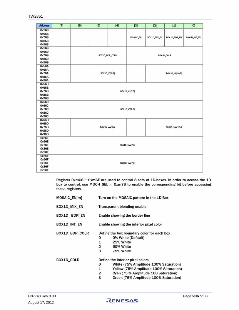
TW2851
FN7743 Rev.0.00 Page 206 of 380
August 17, 2012
Address [7] [6] [5] [4] [3] [2] [1] [0]
0x568
0x668
0x768
0x868
0x968
MOSAIC_EN BOX1D_MIX_EN BOX1D_BDR_EN BOX1D_INT_EN
0x569
0x669
0x769
0x869
0x969
BOX1D_BDR_COLR BOX1D_COLR
0x56A
0x66A
0x76A
0x86A
0x96A
BOX1D_VT[9:8] BOX1D_HL[10:8]
0x56B
0x66B
0x76B
0x86B
0x96B
BOX1D_HL[7:0]
0x56C
0x66C
0x76C
0x86C
0x96C
BOX1D_VT[7:0]
0x56D
0x66D
0x76D
0x86D
0x96D
BOX1D_VW[9:8] BOX1D_HW[10:8]
0x56E
0x66E
0x76E
0x86E
0x96E
BOX1D_HW[7:0]
0x56F
0x66F
0x76F
0x86F
0x96F
BOX1D_VW[7:0]
Register 0xm68 ~ 0xm6F are used to control 8 sets of 1D-boxes. In order to access the 1D
box to control, use MDCH_SEL in 0xm76 to enable the corresponding bit before accessing
these registers.
MOSAIC_EN[m] Turn on the MOSAIC pattern in the 1D Box.
BOX1D_MIX_EN Transparent blending enable
BOX1D_ BDR_EN Enable showing the border line
BOX1D_INT_EN Enable showing the interior pixel color
BOX1D_BDR_COLR Define the box boundary color for each box
0 0% White (Default)
1 25% White
2 50% White
3 75% White
BOX1D_COLR Define the interior pixel colors
0 White (75% Amplitude 100% Saturation)
1 Yellow (75% Amplitude 100% Saturation)
2 Cyan (75 % Amplitude 100 Saturation)
3 Green (75% Amplitude 100% Saturation)

TW2851
FN7743 Rev.0.00 Page 207 of 380
August 17, 2012
4 Magenta (75% Amplitude 100% Saturation)
5 Red (75% Amplitude 100% Saturation)
6 Blue (75% Amplitude 100% Saturation)
7 0% Black
8 100% White
9 50% Gray
10 25% Gray
11 Blue (75% Amplitude 75% Saturation)
12 Defined by CLUT0 in 0xm78, 0xm7C, 0xm80
13 Defined by CLUT1 in 0xm79, 0xm7D, 0xm81
14 Defined by CLUT2 in 0xm7A, 0xm7E, 0xm82
15 Defined by CLUT3 in 0xm7B, 0xm7F, 0xm83
BOX1D_HL Define the horizontal left location of box.
0 Left end (default)
: :
1439 Right end
BOX1D_VT Define the vertical top location of box.
0 Vertical top (default)
: :
899 Vertical bottom
BOX1D_HW Define the horizontal size of box.
0 1 Pixel width (default)
: :
1439 1440 Pixels width
BOX1D_VW Define the vertical size of box.
0 1 Lines height (default)
: :
899 900 Lines height

TW2851
FN7743 Rev.0.00 Page 208 of 380
August 17, 2012
2D BOX CONTROL
Address [7] [6] [5] [4] [3] [2] [1] [0]
0x575
0x675
0x775
0x875
0x975
MDBOX_EN MD_BND_MERG MDBOX_ALPHA
MDBOX_EN Enable the Motion 2D Box function
MD_BND_MERG Turn on the 2D Box merge if two adjacent box are both on
MDBOX_ALPHA Select the alpha blending mode for 2D arrayed Box
0 50% (default)
1 50%
2 75%
3 25%
Address [7] [6] [5] [4] [3] [2] [1] [0]
0x576
0x676
0x776
0x876
0x976
MDCH_SEL
MDCH_SEL Select one of the 8 1DBOXs to configure using 0xm68 ~ 0xm6F or
one of the 8 Motion 2D Boxes to configure using 0xm84 ~ 0xm8F.
Address [7] [6] [5] [4] [3] [2] [1] [0]
0x578
0x678
0x778
0x878
0x978
MD_CLUT0_Y
0x579
0x679
0x779
0x879
0x979
MD_CLUT1_Y
0x57A
0x67A
0x77A
0x87A
0x97A
MD_CLUT2_Y
0x57B
0x67B
0x77B
0x87B
0x97B
MD_CLUT3_Y
0x57C
0x67C
0x77C
0x87C
0x97C
MD_CLUT0_CB
0x57D
0x67D
0x77D
0x87D
0x97D
MD_CLUT1_CB
0x57E
0x67E
0x77E
0x87E
MD_CLUT2_CB

TW2851
FN7743 Rev.0.00 Page 209 of 380
August 17, 2012
Address [7] [6] [5] [4] [3] [2] [1] [0]
0x97E
0x57F
0x67F
0x77F
0x87F
0x97F
MD_CLUT3_CB
0x580
0x680
0x780
0x880
0x980
MD_CLUT0_CR
0x581
0x681
0x781
0x881
0x981
MD_CLUT1_CR
0x582
0x682
0x782
0x882
0x982
MD_CLUT2_CR
0x583
0x683
0x783
0x883
0x983
MD_CLUT3_CR
MD_CLUTx_Y Y component for user defined color 0 (default : 0)
MD_CLUTx_CB Cb component for user defined color 0 (default : 0)
MD_CLUTx_CR Cr component for user defined color 0 (default : 0)
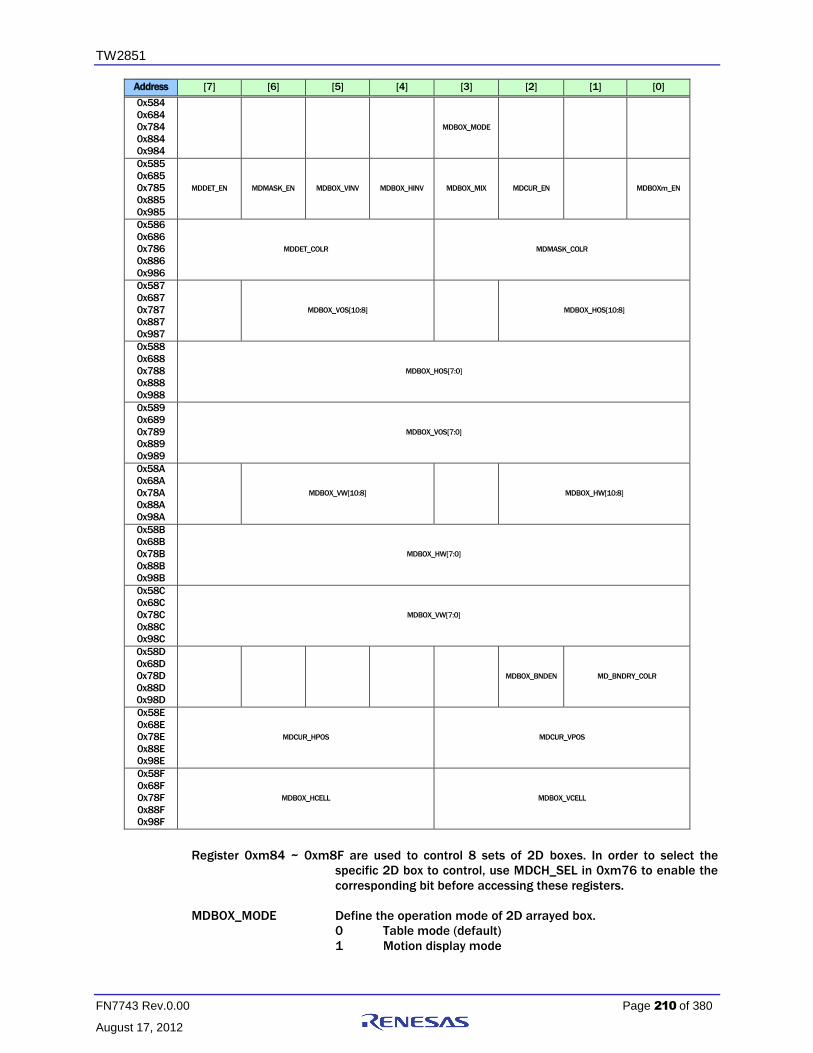
TW2851
FN7743 Rev.0.00 Page 210 of 380
August 17, 2012
Address [7] [6] [5] [4] [3] [2] [1] [0]
0x584
0x684
0x784
0x884
0x984
MDBOX_MODE
0x585
0x685
0x785
0x885
0x985
MDDET_EN MDMASK_EN MDBOX_VINV MDBOX_HINV MDBOX_MIX MDCUR_EN MDBOXm_EN
0x586
0x686
0x786
0x886
0x986
MDDET_COLR MDMASK_COLR
0x587
0x687
0x787
0x887
0x987
MDBOX_VOS[10:8] MDBOX_HOS[10:8]
0x588
0x688
0x788
0x888
0x988
MDBOX_HOS[7:0]
0x589
0x689
0x789
0x889
0x989
MDBOX_VOS[7:0]
0x58A
0x68A
0x78A
0x88A
0x98A
MDBOX_VW[10:8] MDBOX_HW[10:8]
0x58B
0x68B
0x78B
0x88B
0x98B
MDBOX_HW[7:0]
0x58C
0x68C
0x78C
0x88C
0x98C
MDBOX_VW[7:0]
0x58D
0x68D
0x78D
0x88D
0x98D
MDBOX_BNDEN MD_BNDRY_COLR
0x58E
0x68E
0x78E
0x88E
0x98E
MDCUR_HPOS MDCUR_VPOS
0x58F
0x68F
0x78F
0x88F
0x98F
MDBOX_HCELL MDBOX_VCELL
Register 0xm84 ~ 0xm8F are used to control 8 sets of 2D boxes. In order to select the
specific 2D box to control, use MDCH_SEL in 0xm76 to enable the
corresponding bit before accessing these registers.
MDBOX_MODE Define the operation mode of 2D arrayed box.
0 Table mode (default)
1 Motion display mode
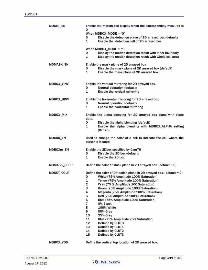
TW2851
FN7743 Rev.0.00 Page 211 of 380
August 17, 2012
MDDET_EN Enable the motion cell display when the corresponding mask bit is
0
When MDBOX_MODE = “0”
0 Disable the detection plane of 2D arrayed box (default)
1 Enable the detection cell of 2D arrayed box
When MDBOX_MODE = “1”
0 Display the motion detection result with inner boundary
1 Display the motion detection result with whole cell area
MDMASK_EN Enable the mask plane of 2D arrayed box
0 Disable the mask plane of 2D arrayed box (default)
1 Enable the mask plane of 2D arrayed box
MDBOX_VINV Enable the vertical mirroring for 2D arrayed box.
0 Normal operation (default)
1 Enable the vertical mirroring
MDBOX_HINV Enable the horizontal mirroring for 2D arrayed box.
0 Normal operation (default)
1 Enable the horizontal mirroring
MDBOX_MIX Enable the alpha blending for 2D arrayed box plane with video
data.
0 Disable the alpha blending (default)
1 Enable the alpha blending with MDBOX_ALPHA setting
(0x575)
MDCUR_EN Used to change the color of a cell to indicate the cell where the
cursor is located
MDBOXm_EN Enable the 2Dbox specified by 0xm76
0 Disable the 2D box (default)
1 Enable the 2D box
MDMASK_COLR Define the color of Mask plane in 2D arrayed box. (default = 0)
MDDET_COLR Define the color of Detection plane in 2D arrayed box. (default = 0)
0 White (75% Amplitude 100% Saturation)
1 Yellow (75% Amplitude 100% Saturation)
2 Cyan (75 % Amplitude 100 Saturation)
3 Green (75% Amplitude 100% Saturation)
4 Magenta (75% Amplitude 100% Saturation)
5 Red (75% Amplitude 100% Saturation)
6 Blue (75% Amplitude 100% Saturation)
7 0% Black
8 100% White
9 50% Gray
10 25% Gray
11 Blue (75% Amplitude 75% Saturation)
12 Defined by CLUT0
13 Defined by CLUT1
14 Defined by CLUT2
15 Defined by CLUT3
MDBOX_VOS Define the vertical top location of 2D arrayed box.

TW2851
FN7743 Rev.0.00 Page 212 of 380
August 17, 2012
0 Vertical top end (default)
: :
900 Vertical bottom end
MDBOX_HOS Define the horizontal left location of 2D arrayed box.
0 Horizontal left end (default)
: :
720 Horizontal right end
MDBOX_VW Define the vertical size of 2D arrayed box.
0 0 Line height (default)
: :
255 255 Line height
MDBOX_HW Define the horizontal size of 2D arrayed box.
0 0 Pixel width (default)
: :
255 510 Pixels width
MDBOX_BNDEN Enable the boundary of 2D arrayed box.
0 Disable the boundary (default)
1 Enable the boundary
MD_BNDRY_COLR Define the color of 2D arrayed box boundary
0 0 % Black (default)
1 25% Gray
2 50% Gray
3 75% White
Define the displayed color for cursor cell and motion-detected
region
0,1 75% White (default)
2,3 0% Black
MDCUR_HPOS Indicate the horizontal location of the cursor cell
MDCUR_VPOS Indicate the vertical location of the cursor cell
MDBOX_HCELL Indicate the number of columns in the 2D box
MDBOX_VCELL Indicate the number of rows in the 2D box

TW2851
FN7743 Rev.0.00 Page 213 of 380
August 17, 2012
CURSOR CONTROL
Address [7] [6] [5] [4] [3] [2] [1] [0]
0x65B CUR_EN
CUR_EN Enable the 5 OSD cursors. Only one of the 5 should be turned on.
Bit 0: Display VGA OSD
Bit 1: Display CVBS OSD
Bit 2: Record 0 OSD
Bit 3: Record 1 OSD
Bit 4: SPOT OSD
Address [7] [6] [5] [4] [3] [2] [1] [0]
0x65C CUR_REV CUR_BLINK CUR_HOLLOW_OFF CUR_CUSTOM_LD CUR_SEL
CUR_REV Reverse the cursor color (black become white, white become
black)
CUR_BLINK Enable blink of mouse pointer.
0 Disable cursor blinking (default)
1 Enable cursor blinking
CUR_HOLLOW_OFF Control interior pixel color of the cursor.
0 Hollow cursor shape (only the border pixels are shown)
(default)
1 Filled with solid color specified by the cursor pixel
CUR_CUSTOM_LD Load the customized cursor shape from DDR memory into the on
chip SRAM
CUR_SEL Select the cursor type
0 Small cursor
1 Normal cursor
2 Customized cursor implemented with SRAM
3 Reserved
Address [7] [6] [5] [4] [3] [2] [1] [0]
0x65D CUR_Y[10:8] CUR_X[10:8]
0x65E CUR_X[7:0]
0x65F CUR_Y[7:0]
CUR_X Control the horizontal location of mouse pointer.
0 0 Pixel position (default)
: :
1440 1440 Pixel position
CUR_Y Control the vertical location of mouse pointer.
0 0 Line position (default)
: :
900 900 Line position

TW2851
FN7743 Rev.0.00 Page 214 of 380
August 17, 2012
Audio CODEC
Address [7] [6] [5] [4] [3] [2] [1] [0]
0xEBA AIGAIN1
0xEBB 0 0 0 0 0 0 0 0
0xEBC 0 0 0 1 0 0 0 0
0xEBD AIGAIN3 AIGAIN2
0xEBE AIGAIN5 AIGAIN4
AIGAIN Select the amplifier’s gain for each analog audio input AIN1 ~
AIN5.
0 0.25
1 0.31
2 0.38
3 0.44
4 0.50
5 0.63
6 0.75
7 0.88
8 1.00 (default)
9 1.25
10 1.50
11 1.75
12 2.00
13 2.25
14 2.50
15 2.75

TW2851
FN7743 Rev.0.00 Page 215 of 380
August 17, 2012
Address [7] [6] [5] [4] [3] [2] [1] [0]
0x062 M_RLSWAP RM_SYNC RM_PBSEL R_ADATM R_MULTCH
M_RLSWAP Define the sequence of mixing and playback audio data on the
ADATM pin
If RM_SYNC=0 : I2S format
0 Mixing audio on position 0 and playback audio on
position 8 (Default)
1 Playback audio on position 0 and mixing audio on
position 8
If RM_SYNC=1 : DSP format
0 Mixing audio on position 0 and playback audio on
position 1 (Default)
1 Playback audio on position 0 and mixing audio on
position 1
RM_SYNC Define the digital serial audio data format for record and mixing
audio on the ACLKR, ASYNR, ADATR and ADATM pin
0 I2S format (Default)
1 DSP format
RM_PBSEL Select the output PlayBackIn data for the ADATM pin
0 First Stage PlayBackIn audio (Default)
1 Second Stage PlayBackIn audio
2 Third Stage PlayBackIn audio
3 Last Stage PlayBackIn audio
R_ADATM Select the output mode for the ADATM pin
0 Digital serial data of mixing audio (Default)
1 Digital serial data of ADATR format record audio
2 Digital serial data of ADATM format record audio
R_MULTCH Define the number of audio for record on the ADATR pin
0 2 audios (Default)
1 4 audios
2 8 audios
3 16 audios
Number of output data are limited as shown on Sequence of Multi-
channel Audio Record table. Also, each output position data are
selected by R_SEQ_0/R_SEQ_1/…/R_SEQ_F registers.
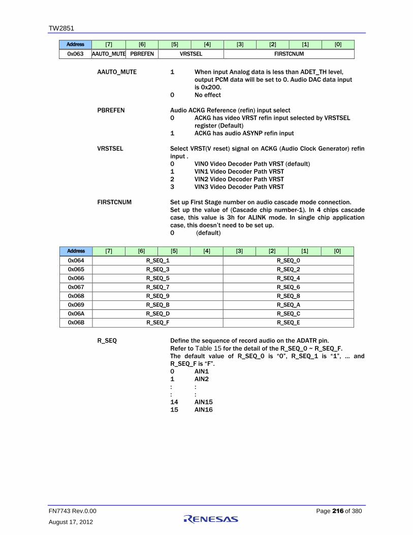
TW2851
FN7743 Rev.0.00 Page 216 of 380
August 17, 2012
Address [7] [6] [5] [4] [3] [2] [1] [0]
0x063 AAUTO_MUTE PBREFEN VRSTSEL FIRSTCNUM
AAUTO_MUTE 1 When input Analog data is less than ADET_TH level,
output PCM data will be set to 0. Audio DAC data input
is 0x200.
0 No effect
PBREFEN Audio ACKG Reference (refin) input select
0 ACKG has video VRST refin input selected by VRSTSEL
register (Default)
1 ACKG has audio ASYNP refin input
VRSTSEL Select VRST(V reset) signal on ACKG (Audio Clock Generator) refin
input .
0 VIN0 Video Decoder Path VRST (default)
1 VIN1 Video Decoder Path VRST
2 VIN2 Video Decoder Path VRST
3 VIN3 Video Decoder Path VRST
FIRSTCNUM Set up First Stage number on audio cascade mode connection.
Set up the value of (Cascade chip number-1). In 4 chips cascade
case, this value is 3h for ALINK mode. In single chip application
case, this doesn’t need to be set up.
0 (default)
Address [7] [6] [5] [4] [3] [2] [1] [0]
0x064 R_SEQ_1 R_SEQ_0
0x065 R_SEQ_3 R_SEQ_2
0x066 R_SEQ_5 R_SEQ_4
0x067 R_SEQ_7 R_SEQ_6
0x068 R_SEQ_9 R_SEQ_8
0x069 R_SEQ_B R_SEQ_A
0x06A R_SEQ_D R_SEQ_C
0x06B R_SEQ_F R_SEQ_E
R_SEQ Define the sequence of record audio on the ADATR pin.
Refer to Table 15 for the detail of the R_SEQ_0 ~ R_SEQ_F.
The default value of R_SEQ_0 is “0”, R_SEQ_1 is “1”, … and
R_SEQ_F is “F”.
0 AIN1
1 AIN2
: :
: :
14 AIN15
15 AIN16
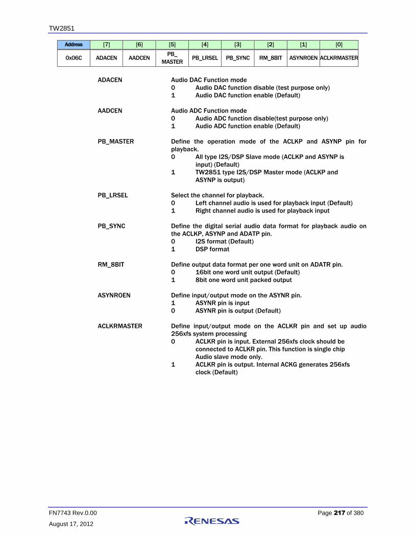
TW2851
FN7743 Rev.0.00 Page 217 of 380
August 17, 2012
Address [7] [6] [5] [4] [3] [2] [1] [0]
0x06C ADACEN AADCEN PB_
MASTER PB_LRSEL PB_SYNC RM_8BIT ASYNROEN ACLKRMASTER
ADACEN Audio DAC Function mode
0 Audio DAC function disable (test purpose only)
1 Audio DAC function enable (Default)
AADCEN Audio ADC Function mode
0 Audio ADC function disable(test purpose only)
1 Audio ADC function enable (Default)
PB_MASTER Define the operation mode of the ACLKP and ASYNP pin for
playback.
0 All type I2S/DSP Slave mode (ACLKP and ASYNP is
input) (Default)
1 TW2851 type I2S/DSP Master mode (ACLKP and
ASYNP is output)
PB_LRSEL Select the channel for playback.
0 Left channel audio is used for playback input (Default)
1 Right channel audio is used for playback input
PB_SYNC Define the digital serial audio data format for playback audio on
the ACLKP, ASYNP and ADATP pin.
0 I2S format (Default)
1 DSP format
RM_8BIT Define output data format per one word unit on ADATR pin.
0 16bit one word unit output (Default)
1 8bit one word unit packed output
ASYNROEN Define input/output mode on the ASYNR pin.
1 ASYNR pin is input
0 ASYNR pin is output (Default)
ACLKRMASTER Define input/output mode on the ACLKR pin and set up audio
256xfs system processing
0 ACLKR pin is input. External 256xfs clock should be
connected to ACLKR pin. This function is single chip
Audio slave mode only.
1 ACLKR pin is output. Internal ACKG generates 256xfs
clock (Default)
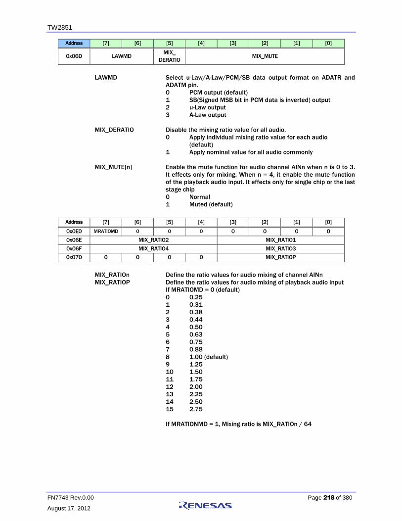
TW2851
FN7743 Rev.0.00 Page 218 of 380
August 17, 2012
Address [7] [6] [5] [4] [3] [2] [1] [0]
0x06D LAWMD MIX_
DERATIO MIX_MUTE
LAWMD Select u-Law/A-Law/PCM/SB data output format on ADATR and
ADATM pin.
0 PCM output (default)
1 SB(Signed MSB bit in PCM data is inverted) output
2 u-Law output
3 A-Law output
MIX_DERATIO Disable the mixing ratio value for all audio.
0 Apply individual mixing ratio value for each audio
(default)
1 Apply nominal value for all audio commonly
MIX_MUTE[n] Enable the mute function for audio channel AINn when n is 0 to 3.
It effects only for mixing. When n = 4, it enable the mute function
of the playback audio input. It effects only for single chip or the last
stage chip
0 Normal
1 Muted (default)
Address [7] [6] [5] [4] [3] [2] [1] [0]
0x0E0 MRATIOMD 0 0 0 0 0 0 0
0x06E MIX_RATIO2 MIX_RATIO1
0x06F MIX_RATIO4 MIX_RATIO3
0x070 0 0 0 0 MIX_RATIOP
MIX_RATIOn Define the ratio values for audio mixing of channel AINn
MIX_RATIOP Define the ratio values for audio mixing of playback audio input
If MRATIOMD = 0 (default)
0 0.25
1 0.31
2 0.38
3 0.44
4 0.50
5 0.63
6 0.75
7 0.88
8 1.00 (default)
9 1.25
10 1.50
11 1.75
12 2.00
13 2.25
14 2.50
15 2.75
If MRATIONMD = 1, Mixing ratio is MIX_RATIOn / 64

TW2851
FN7743 Rev.0.00 Page 219 of 380
August 17, 2012
Address [7] [6] [5] [4] [3] [2] [1] [0]
0x071 V_ADC_CKPOL A_ADC_CKPOL A_DAC_CKPOL MIX_OUTSEL
V_ADC_CKPOL Test purpose only (Default 0)
A_ADC_CKPOL Test purpose only (Default 0)
A_DAC_CKPOL Test purpose only (Default 0)
MIX_OUTSEL Define the final audio output for analog and digital mixing out.
0 Select record audio of channel 1
1 Select record audio of channel 2
2 Select record audio of channel 3
3 Select record audio of channel 4
4 Select record audio of channel 5
5 Select record audio of channel 6
6 Select record audio of channel 7
7 Select record audio of channel 8
8 Select record audio of channel 9
9 Select record audio of channel 10
10 Select record audio of channel 11
11 Select record audio of channel 12
12 Select record audio of channel 13
13 Select record audio of channel 14
14 Select record audio of channel 15
15 Select record audio of channel 16
16 Select playback audio of the first stage chip
17 Select playback audio of the second stage chip
18 Select playback audio of the third stage chip
19 Select playback audio of the last stage chip
20 Select mixed audio (default)
21 Select record audio of channel AIN51
22 Select record audio of channel AIN52
23 Select record audio of channel AIN53
24 Select record audio of channel AIN54

TW2851
FN7743 Rev.0.00 Page 220 of 380
August 17, 2012
Address [7] [6] [5] [4] [3] [2] [1] [0]
0x072 AAMPMD ADET_FILT ADET_TH4[4] ADET_TH3[4] ADET_TH2[4] ADET_TH1[4]
0x073 ADET_TH2[3:0] ADET_TH1[3:0]
0x074 ADET_TH4[3:0] ADET_TH3[3:0]
AAMPMD Define the audio detection method.
0 Detect audio if absolute amplitude is greater than
threshold
1 Detect audio if differential amplitude is greater than
Threshold (default)
ADET_FILT Select the filter for audio detection (default 4h)
0 Wide LPF
: :
7 Narrow LPF
ADET_THn Define the threshold value for audio detection of AINn (Default Ah)
0 Low value
: :
31 High value
If fs = 8kHz Audio Clock setting mode, Registers
0x072 = 0xC0
0x073 = 0xAA
0x074 = 0xAA
are typical setting.
If fs=16kHz/32kHz/44.1kHz/48kHz Audio Clock setting mode,
Registers
0x072 = 0xE0
0x073 = 0xBB
0x074 = 0xBB
are typical setting.
Address [7] [6] [5] [4] [3] [2] [1] [0]
0x075 ACKI[7:0]
0x076 ACKI[15:8]
0x077 0 0 ACKI[21:16]
ACKI These bits control ACKI Clock Increment in ACKG block.
09B583h for fs = 8kHz is default
Address [7] [6] [5] [4] [3] [2] [1] [0]
0x078 ACKN[7:0]
0x079 ACKN[15:8]
0x07A 0 0 0 0 0 0 ACKN[17:16]
ACKN These bits control ACKN Clock Number in ACKG block..
000100h for Playback Slave-in lock is default.
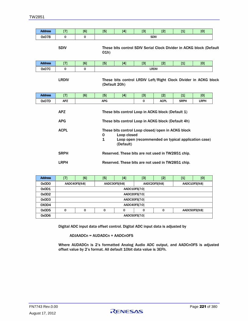
TW2851
FN7743 Rev.0.00 Page 221 of 380
August 17, 2012
Address [7] [6] [5] [4] [3] [2] [1] [0]
0x07B 0 0 SDIV
SDIV These bits control SDIV Serial Clock Divider in ACKG block (Default
01h)
Address [7] [6] [5] [4] [3] [2] [1] [0]
0x07C 0 0 LRDIV
LRDIV These bits control LRDIV Left/Right Clock Divider in ACKG block
(Default 20h)
Address [7] [6] [5] [4] [3] [2] [1] [0]
0x07D APZ APG 0 ACPL SRPH LRPH
APZ These bits control Loop in ACKG block (Default 1)
APG These bits control Loop in ACKG block (Default 4h)
ACPL These bits control Loop closed/open in ACKG block
0 Loop closed
1 Loop open (recommended on typical application case)
(Default)
SRPH Reserved. These bits are not used in TW2851 chip.
LRPH Reserved. These bits are not used in TW2851 chip.
Address [7] [6] [5] [4] [3] [2] [1] [0]
0x0D0 AADC4OFS[9:8] AADC3OFS[9:8] AADC2OFS[9:8] AADC1OFS[9:8]
0x0D1 AADC1OFS[7:0]
0x0D2 AADC2OFS[7:0]
0x0D3 AADC3OFS[7:0]
0X0D4 AADC4OFS[7:0]
0x0D5 0 0 0 0 0 0 AADC5OFS[9:8]
0x0D6 AADC5OFS[7:0]
Digital ADC input data offset control. Digital ADC input data is adjusted by
ADJAADCn = AUDADCn + AADCnOFS
Where AUDADCn is 2’s formatted Analog Audio ADC output, and AADCnOFS is adjusted
offset value by 2’s format. All default 10bit data value is 3EFh.

TW2851
FN7743 Rev.0.00 Page 222 of 380
August 17, 2012
Address [7] [6] [5] [4] [3] [2] [1] [0]
0x0D7 0 ADCISEL AUDADCn[9:8]* ADJAADCn[9:8]*
0x0D8 AUDADCn[7:0]*
0x0D9 ADJAADCn[7:0]*
AUDADCn Current Analog Audio n ADC Digital Output Value by 2’s format
` These value show the first input data value in front of Digital Audio
Decimation Filtering process.
ADJAADCn Current adjusted Audio ADC Digital input data value by 2’s format.
These value show the first input data value in front of Digital Audio
Decimation Filtering process.
ADCISEL Select AUDADCn, ADJAADCn Audio input number. AUDADCn and
ADJAADCn read value shows following selected Audio input data.
0 AIN1
1 AIN2
2 AIN3
3 AIN4
4 AIN5

TW2851
FN7743 Rev.0.00 Page 223 of 380
August 17, 2012
Address [7] [6] [5] [4] [3] [2] [1] [0]
0x0DA 0 0 0 I2SO_RSEL
0x0DB 0 0 0 I2SO_LSEL
0x0DC I2SRECSEL53 I2SRECSEL52 I2SRECSEL51 I2SRECSEL50
0x0DD A5OUT_OFF ADATM_
I2SOEN
MIX_MUTE
_A5 ADET_TH5
A5OUT_OFF AIN5 data output control on ADATR record signal.
0 Output AIN51/AIN52/AIN53/AIN54 record data on ADATR
1 Not output AIN51/AIN52/AIN53/AIN54 record data on
ADATR
ADATM_I2SOEN Define ADATM pin output 2 word data to make standard I2S
output.
0 Output Mixing or Playback data only on
ADATM pin as specified by M_RLSWAP register
(Default)
1 L/R data on ADATM pin is selected by
I2SO_RSEL/I2SO_LSEL registers
MIX_MUTE_A5 Audio input AIN5 mute function control
0 Normal
1 Muted
ADET_TH5 AIN5 threshold value for audio detection
I2SO_RSEL/ Select L/R output data on ADATM pin when ADATM_I2SOEN=1.
I2SO_LSEL Both I2SO_RSEL and I2SO_LSEL select output data by following
order.
0 Select record audio of channel 1(AIN0)
1 Select record audio of channel 2(AIN1)
2 Select record audio of channel 3(AIN2)
3 Select record audio of channel 4(AIN3)
4 Select record audio of channel 5(AIN4)
5 Select record audio of channel 6(AIN5)
6 Select record audio of channel 7(AIN6)
7 Select record audio of channel 8(AIN7)
8 Select record audio of channel 9(AIN8)
9 Select record audio of channel 10(AIN9)
10(Ah) Select record audio of channel 11(AIN10)
11(Bh) Select record audio of channel 12(AIN11)
12(Ch) Select record audio of channel 13(AIN12)
13(Dh) Select record audio of channel 14(AIN13)
14(Eh) Select record audio of channel 15(AIN14)
15(Fh) Select record audio of channel 16(AIN15)
16(10h) Select playback audio of the first stage chip (PB1)
17(11h) Select playback audio of the second stage chip (PB2)
18(12h) Select playback audio of the third stage chip (PB3)
19(13h) Select playback audio of the last stage chip (PB4)
20(14h) Select mixed audio
21(15h) Select record audio of channel 51(AIN51) (default)
22(16h) Select record audio of channel 52(AIN52)
23(17h) Select record audio of channel 53(AIN53)
24(18h) Select record audio of channel 54(AIN54)
Others No audio output
I2SRECSEL5n Select output data of port n in the position below

TW2851
FN7743 Rev.0.00 Page 224 of 380
August 17, 2012
0 AIN51
1 AIN52
2 AIN53
3 AIN54
Address [7] [6] [5] [4] [3] [2] [1] [0]
0x0DE MIX_RATIO5
MIX_RATIO5 Define the ratio values for audio mixing of channel AIN4 using
MIX_RATIO4 to the ratio values for audio mixing of playback audio
input
If MRATIOMD = 0 (default)
0 0.25
1 0.31
2 0.38
3 0.44
4 0.50
5 0.63
6 0.75
7 0.88
8 1.00 (default)
9 1.25
10 1.50
11 1.75
12 2.00
13 2.25
14 2.50
15 2.75
If MRATIONMD = 1, Mixing ratio is MIX_RATIO4 / 64

TW2851
FN7743 Rev.0.00 Page 225 of 380
August 17, 2012
Address [7] [6] [5] [4] [3] [2] [1] [0]
0x0DF ATHROUG
H
ASYNSERI
AL ACLKR128 ACLKR64 AFS384 AIN5MD 0 0
ATHROUGH Default 0
ASYNSERIAL Default 0
ACLKR128 ACLKR clock output mode for special 16x8bit (total 128bit) data
interface.
0 ACLKR output is normal (Default).
1 the number of ACLKR clock per fs is 128.This function is
effective with RM_8BIT=1 8bit mode (special purpose).
ACLKR64 ACLKR clock output mode for special 4 word output interface.
ACLKRMASTER=1 mode only.
0 ACLKR output is normal (Default)
1 the number of ACLKR clock per fs is 64.
AFS384 Special Audio fs Sampling mode.
0 Audio fs Sampling mode is normal 256xfs if AIN5 = 0.
(Default)
1 Audio fs Sampling mode is 384xfs mode. In this mode,
AIMANU=1, A1NUM=0, A2NUM=1, A3NUM=2, A4NUM
= 3, A5NUM=4 setting are needed.
AIN5MD Audio Input process mode
0 AIN1/AIN2/AIN3/AIN4 4 audio input mode. This mode is
256xfs if AFS384 = 0. In this mode, AIN5 is not used.
1 AIN1/AIN2/AIN3/AIN4/AIN5 5 audio input mode. This
mode is 320xfs mode if AFS384 = 0.
Address [7] [6] [5] [4] [3] [2] [1] [0]
0x0E0 MRATIOMD ADACTEST 0 0 0 0 0 0
MRATIOMD 1 Use a more exponential way to interpret the MRATIO.
Perform the following transformation before using the
ratio
0 ~ 3 => 4 ~ 7
4 ~ 7 => 8 ~ 14
8 ~ 11 => 16 ~ 28
12 ~ 15 => 32 ~ 44
0 Use the MRATIO as the ratio
ADACTEST Test feature for ADAC. Set to 0.
Address [7] [6] [5] [4] [3] [2] [1] [0]
0x0E3 0 0 ACLKRPOL ACLKPPOL AFAUTO AFMD
ACLKRPOL ACLKR input signal polarity inverse.
0 Not inversed (Default)
1 Inversed
ACLKPPOL ACLKP input signal polarity inverse.

TW2851
FN7743 Rev.0.00 Page 226 of 380
August 17, 2012
0 Not inversed (Default)
1 Inversed
AFAUTO ACKI[21:0] control automatic set up with AFMD registers
This mode is only effective when ACLKRMASTER=1
0 ACKI[21:0] registers set up ACKI control
1 ACKI control is automatically set up by AFMD register
values
AFMD AFAUTO control mode
0 8kHz setting (Default)
1 16kHz setting
2 32kHz setting
3 44.1kHz setting
4 48kHz setting
Address [7] [6] [5] [4] [3] [2] [1] [0]
0x0E4 I2S8MODE MASCKMD PBINSWAP ASYNRDLY ASYNPDLY ADATPDLY INLAWMD
I2S8MODE 8bit I2S Record output mode.
0 L/R half length separated output (Default).
1 One continuous packed output equal to DSP output
format.
MASCKMD Audio Clock Master ACLKR output wave format.
0 High period is one 27MHz clock period (default).
1 Almost duty 50-50% clock output on ACLKR pin. If this
mode is selected, two times bigger number value need
to be set up on the ACKI register. If AFAUTO=1, ACKI
control is automatically set up even if MASCKMD=1.
PBINSWAP Playback ACLKP/ASYNP/ADATP input data MSB-LSB
swapping.
0 Not swapping
1 Swapping.
ASYNRDLY ASYNR input signal delay.
0 No delay
1 Add one 27MHz period delay in ASYNR signal input
ASYNPDLY ASYNP input signal delay.
0 no delay
1 add one 27MHz period delay in ASYNP signal input
ADATPDLY ADATP input data delay by one ACLKP clock.
0 No delay (Default).This is for I2S type 1T delay input
interface.
1 Add 1 ACLKP clock delay in ADATP input data. This is
for left-justified type 0T delay input interface.
INLAWMD Select u-Law/A-Law/PCM/SB data input format on ADATP pin.
0 PCM input (Default)
1 SB (Signed MSB bit in PCM data is inverted) input
2 u-Law input
3 A-Law input
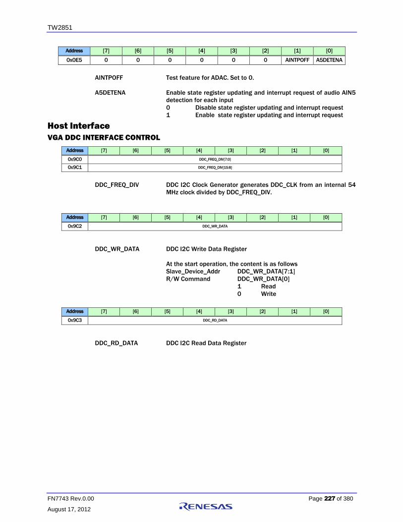
TW2851
FN7743 Rev.0.00 Page 227 of 380
August 17, 2012
Address [7] [6] [5] [4] [3] [2] [1] [0]
0x0E5 0 0 0 0 0 0 AINTPOFF A5DETENA
AINTPOFF Test feature for ADAC. Set to 0.
A5DETENA Enable state register updating and interrupt request of audio AIN5
detection for each input
0 Disable state register updating and interrupt request
1 Enable state register updating and interrupt request
Host Interface
VGA DDC INTERFACE CONTROL
Address [7] [6] [5] [4] [3] [2] [1] [0]
0x9C0 DDC_FREQ_DIV[7:0]
0x9C1 DDC_FREQ_DIV[15:8]
DDC_FREQ_DIV DDC I2C Clock Generator generates DDC_CLK from an internal 54
MHz clock divided by DDC_FREQ_DIV.
Address [7] [6] [5] [4] [3] [2] [1] [0]
0x9C2 DDC_WR_DATA
DDC_WR_DATA DDC I2C Write Data Register
At the start operation, the content is as follows
Slave_Device_Addr DDC_WR_DATA[7:1]
R/W Command DDC_WR_DATA[0]
1 Read
0 Write
Address [7] [6] [5] [4] [3] [2] [1] [0]
0x9C3 DDC_RD_DATA
DDC_RD_DATA DDC I2C Read Data Register

TW2851
FN7743 Rev.0.00 Page 228 of 380
August 17, 2012
Address [7] [6] [5] [4] [3] [2] [1] [0]
0x9C4 DDC_COMMAND
DDC_COMMAND DDC Control Command (Read/Write)
7 I2C Start
6 I2C Stop
5 Read the value from the slave device register.
Once acknowledged, the data will be in DDC_RD_DATA
Register
4 Write the value in DDC_WR_DATA onto DDC_DATA bus
3 Send an ACK to the DDC_DATA bus when read
2 Clock Count Enable
1 Interrupt Enable
0 Interrupt Acknowledge
Address [7] [6] [5] [4] [3] [2] [1] [0]
0x9C5 DDC_STATUS
DDC_STATUS DDC Status Register (read only)
Bit 7 RXACK
Bit 6 I2C_BUSY
Bit 5 Active Low
Bit 4 0
Bit 3 0
Bit 2 0
Bit 1 I2C Read/Write
Bit 0 Interrupt Acknowledge
Address [7] [6] [5] [4] [3] [2] [1] [0]
0x9C7 0
Reserved Should be kept 0
Address [7] [6] [5] [4] [3] [2] [1] [0]
0x9CF DDC_RST
DDC_RST DDC Software Reset whenever CPU issues a write to this address
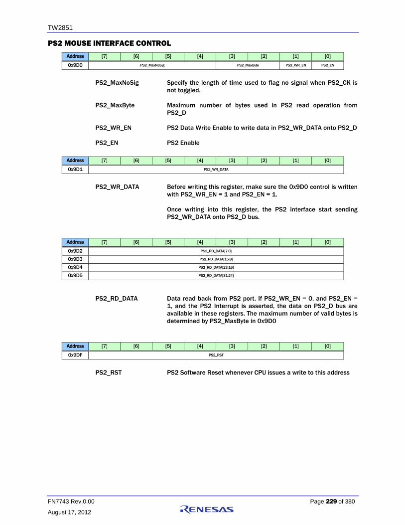
TW2851
FN7743 Rev.0.00 Page 229 of 380
August 17, 2012
PS2 MOUSE INTERFACE CONTROL
Address [7] [6] [5] [4] [3] [2] [1] [0]
0x9D0 PS2_MaxNoSig PS2_MaxByte PS2_WR_EN PS2_EN
PS2_MaxNoSig Specify the length of time used to flag no signal when PS2_CK is
not toggled.
PS2_MaxByte Maximum number of bytes used in PS2 read operation from
PS2_D
PS2_WR_EN PS2 Data Write Enable to write data in PS2_WR_DATA onto PS2_D
PS2_EN PS2 Enable
Address [7] [6] [5] [4] [3] [2] [1] [0]
0x9D1 PS2_WR_DATA
PS2_WR_DATA Before writing this register, make sure the 0x9D0 control is written
with PS2_WR_EN = 1 and PS2_EN = 1.
Once writing into this register, the PS2 interface start sending
PS2_WR_DATA onto PS2_D bus.
Address [7] [6] [5] [4] [3] [2] [1] [0]
0x9D2 PS2_RD_DATA[7:0]
0x9D3 PS2_RD_DATA[15:8]
0x9D4 PS2_RD_DATA[23:16]
0x9D5 PS2_RD_DATA[31:24]
PS2_RD_DATA Data read back from PS2 port. If PS2_WR_EN = 0, and PS2_EN =
1, and the PS2 Interrupt is asserted, the data on PS2_D bus are
available in these registers. The maximum number of valid bytes is
determined by PS2_MaxByte in 0x9D0
Address [7] [6] [5] [4] [3] [2] [1] [0]
0x9DF PS2_RST
PS2_RST PS2 Software Reset whenever CPU issues a write to this address

TW2851
FN7743 Rev.0.00 Page 230 of 380
August 17, 2012
INTERRUPT
Address [7] [6] [5] [4] [3] [2] [1] [0]
0x1D0 INTERRUPT_VECT0
0x1D1 INTERRUPT_VECT1
0x1D2 INTERRUPT_VECT2
0x1D3 INTERRUPT_VECT3
0x1D4 INTERRUPT_VECT4
0x1D5 INTERRUPT_VECT5
0x1D6 INTERRUPT_VECT6
0x1D7 INTERRUPT_VECT7
0x1D8 INTERRUPT_VECT_MASK0
0x1D9 INTERRUPT_VECT_MASK1
0x1DA INTERRUPT_VECT_MASK2
0x1DB INTERRUPT_VECT_MASK3
0x1DC INTERRUPT_VECT_MASK4
0x1DD INTERRUPT_VECT_MASK5
0x1DE INTERRUPT_VECT_MASK6
0x1DF INTERRUPT_VECT_MASK7
0x1E0 INTERRUPT_STATUS
INTERRUPT_VECTn Read Read the interrupt status of the specific interrupt source
Write Write a ‘1’ to that bit will clear the specific interrupt
source. This clear bit will make the INTERRUPT_VECT
to become ‘0’
INTERRUPT_VECT_MASKn
1 Set to ‘1’ will allow the INTERRUPT_VECT source to
show up at the output IRQ pin if the vector bit is a ‘1’
0 Set to ‘0’ will disable the output to IRQ, so the MCU will
ignore that source
INTERRUPT_STATUS[x]
1 An INTERRUPT_STATUS[x] of ‘1’ means there is some
source in INTERRUPT_VECTx set to 1. The MCU can read
this register before it read each of the INTERRUPT_VECTx.
The specific interrupt vector is organized as follows:
INTERRUPT_VECT0[3:0] Video Decoder Motion
Detection, ANA_SW = 0
INTERRUPT_VECT0[7:4] Video Decoder Motion
Detection, ANA_SW = 1
INTERRUPT_VECT1[3:0] Video Decoder Night Detection,
ANA_SW = 0
INTERRUPT_VECT1[7:4] Video Decoder Night Detection,
ANA_SW = 1
INTERRUPT_VECT2[3:0] Video Decoder Black Detection,
ANA_SW = 0
INTERRUPT_VECT2[7:4] Video Decoder Black Detection,
ANA_SW = 1
INTERRUPT_VECT3[3:0] Video Decoder NO VIDEO
detection, ANA_SW = 0
INTERRUPT_VECT3[7:4] Video Decoder NO VIDEO
detection, ANA_SW = 1
INTERRUPT_VECT4[3:0] Unused
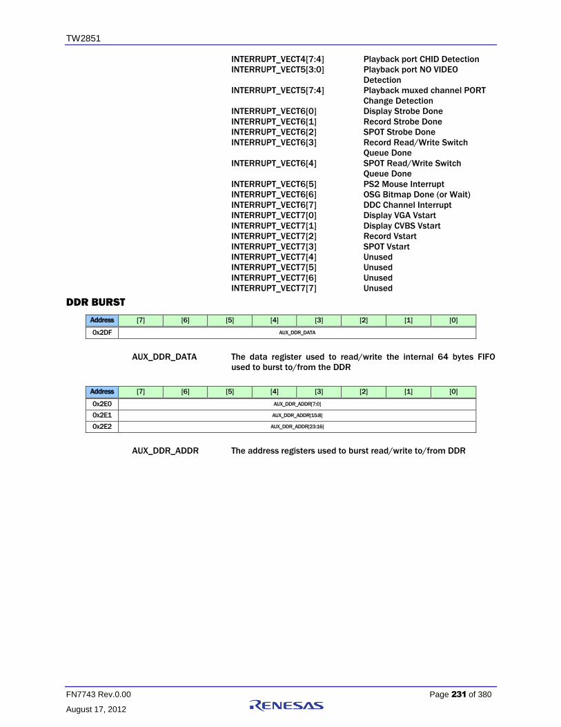
TW2851
FN7743 Rev.0.00 Page 231 of 380
August 17, 2012
INTERRUPT_VECT4[7:4] Playback port CHID Detection
INTERRUPT_VECT5[3:0] Playback port NO VIDEO
Detection
INTERRUPT_VECT5[7:4] Playback muxed channel PORT
Change Detection
INTERRUPT_VECT6[0] Display Strobe Done
INTERRUPT_VECT6[1] Record Strobe Done
INTERRUPT_VECT6[2] SPOT Strobe Done
INTERRUPT_VECT6[3] Record Read/Write Switch
Queue Done
INTERRUPT_VECT6[4] SPOT Read/Write Switch
Queue Done
INTERRUPT_VECT6[5] PS2 Mouse Interrupt
INTERRUPT_VECT6[6] OSG Bitmap Done (or Wait)
INTERRUPT_VECT6[7] DDC Channel Interrupt
INTERRUPT_VECT7[0] Display VGA Vstart
INTERRUPT_VECT7[1] Display CVBS Vstart
INTERRUPT_VECT7[2] Record Vstart
INTERRUPT_VECT7[3] SPOT Vstart
INTERRUPT_VECT7[4] Unused
INTERRUPT_VECT7[5] Unused
INTERRUPT_VECT7[6] Unused
INTERRUPT_VECT7[7] Unused
DDR BURST
Address [7] [6] [5] [4] [3] [2] [1] [0]
0x2DF AUX_DDR_DATA
AUX_DDR_DATA The data register used to read/write the internal 64 bytes FIFO
used to burst to/from the DDR
Address [7] [6] [5] [4] [3] [2] [1] [0]
0x2E0 AUX_DDR_ADDR[7:0]
0x2E1 AUX_DDR_ADDR[15:8]
0x2E2 AUX_DDR_ADDR[23:16]
AUX_DDR_ADDR The address registers used to burst read/write to/from DDR

TW2851
FN7743 Rev.0.00 Page 232 of 380
August 17, 2012
Address [7] [6] [5] [4] [3] [2] [1] [0]
0x2E3 AUX_DDR_LENGTH[7:0]
0x2E4 AUX_WAIT_POL AUX_DDR_LENGTH[10:8] AUX_FIFO_EMPTY* AUX_FIFO_FULL* AUX_DDR_RD AUX_DDR_WR
AUX_DDR_LENGTH Specify the length of the CPU burst read/write to/from DDR. The
Maximum length is 1204 bytes
AUX_WAIT_POL Reverse the polarity of the AUX WAIT signal
AUX_FIFO_EMPTY The internal 64 bytes FIFO emptiness status flag
1 The 64 bytes internal FIFO is empty and available
for writing data to burst to DDR
0 The 64 bytes internal FIFO is not empty, meaning
the previous move from FIFO to DDR is not
completed yet. The CPU should wait until this bit is
set before writing a new 64 bytes.
AUX_FIFO_FULL The internal 64 bytes FIFO has data available for CPU to read
This bit allows the CPU to poll after an AUX_DDR_RD command is
issued, or after every 64 bytes of data are read. With this bit set,
the CPU is safe to read up to 64 bytes, or up to the last burst
length derived from the AUX_DDR_LENGTH
1 The 64 bytes internal FIFO has some data
Available for CPU to read
0 The 64 bytes internal FIFO does not have data
for CPU to read yet
AUX_DDR_WR The AUX DDR Write Command. This bit is self-cleared
AUX_DDR_RD The AUX DDR Read Command. This bit is self-cleared.
DDR Memory Controller
Address [7] [6] [5] [4] [3] [2] [1] [0]
0x2E5 DDR_RD_CLK_SEL DDR_DQS_RD_DLY DDR_RD_TO_WR_NOP
DDR_RD_CLK_SEL Select the DQS or ~DQS as read clock to latch the DQ
DDR_DQS_RD_DLY Select the DQS valid read data cycle delay number
DDR_RD_TO_WR_NOP
DDR read to write adds additional nop cycles. Default 0

TW2851
FN7743 Rev.0.00 Page 233 of 380
August 17, 2012
Address [7] [6] [5] [4] [3] [2] [1] [0]
0x2E6 DDR_DQS_SEL0
0x2E7 DDR_DQS_SEL1
0x2E8 OSG_DDR_TIMER DDR_CLK90_SEL
DDR_DQS_SEL0 Select DDR_DQS_SEL/32 clock phase delay
DDR_DQS_SEL1 Select DDR_DQS_SEL/32 clock phase delay
DDR_CLK90_SEL Select the phase of 90 degree CLK generated from DLL.
The phase is DDR_CLK90_SEL/32
OSG_DDR_TIMER Timer to slow down the OSG write to avoid excessive peak
bandwidth
Address [7] [6] [5] [4] [3] [2] [1] [0]
0x2E9 DDR_DLL_TEST_SEL DDR_DLL_DEBUG_SEL DDR_DLL_TAP_S
DDR_DLL_DEBUG_SEL
Debug select to the DLL Debug Output
DDR_DLL_TEST_SEL Select the DLL test output signal
DDR_DLL_TAP_S Select the DLL TAPS
Address [7] [6] [5] [4] [3] [2] [1] [0]
0x2EA DDR_T_RC DDR_T_RAS
0x2EB DDR_T_RFC DDR_T_RP
0x2EC DDR_T_RCD DDR_T_WR
DDR_T_RC DDR t_rc timing
DDR_T_RAS DDR t_ras timing
DDR_T_RFC DDR t_rfc timing
DDR_T_RP DDR t_rp timing
DDR_T_RCD DDR t_rcd timing
DDR_T_WR DDR t_wr timing
Address [7] [6] [5] [4] [3] [2] [1] [0]
0x2ED DDR_REFRESH DDR_INIT_BYPASS DDR_B_LENGTH
DDR_REFRESH DDR refresh timing control
DDR_INIT_BYPASS DDR initialization bypass (for simulation purpose only)
DDR_B_LENGTH DDR burst length
Address [7] [6] [5] [4] [3] [2] [1] [0]
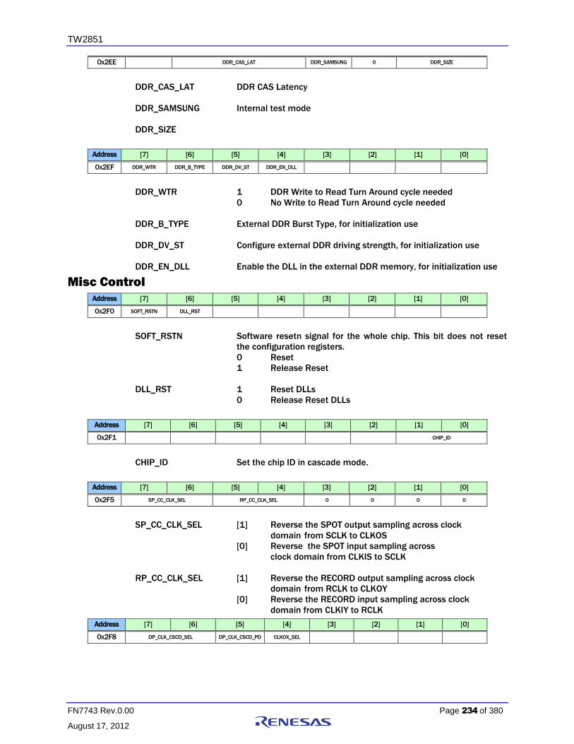
TW2851
FN7743 Rev.0.00 Page 234 of 380
August 17, 2012
0x2EE DDR_CAS_LAT DDR_SAMSUNG 0 DDR_SIZE
DDR_CAS_LAT DDR CAS Latency
DDR_SAMSUNG Internal test mode
DDR_SIZE
Address [7] [6] [5] [4] [3] [2] [1] [0]
0x2EF DDR_WTR DDR_B_TYPE DDR_DV_ST DDR_EN_DLL
DDR_WTR 1 DDR Write to Read Turn Around cycle needed
0 No Write to Read Turn Around cycle needed
DDR_B_TYPE External DDR Burst Type, for initialization use
DDR_DV_ST Configure external DDR driving strength, for initialization use
DDR_EN_DLL Enable the DLL in the external DDR memory, for initialization use
Misc Control
Address [7] [6] [5] [4] [3] [2] [1] [0]
0x2F0 SOFT_RSTN DLL_RST
SOFT_RSTN Software resetn signal for the whole chip. This bit does not reset
the configuration registers.
0 Reset
1 Release Reset
DLL_RST 1 Reset DLLs
0 Release Reset DLLs
Address [7] [6] [5] [4] [3] [2] [1] [0]
0x2F1 CHIP_ID
CHIP_ID Set the chip ID in cascade mode.
Address [7] [6] [5] [4] [3] [2] [1] [0]
0x2F5 SP_CC_CLK_SEL RP_CC_CLK_SEL 0 0 0 0
SP_CC_CLK_SEL [1] Reverse the SPOT output sampling across clock
domain from SCLK to CLKOS
[0] Reverse the SPOT input sampling across
clock domain from CLKIS to SCLK
RP_CC_CLK_SEL [1] Reverse the RECORD output sampling across clock
domain from RCLK to CLKOY
[0] Reverse the RECORD input sampling across clock
domain from CLKIY to RCLK
Address [7] [6] [5] [4] [3] [2] [1] [0]
0x2F8 DP_CLK_CSCD_SEL DP_CLK_CSCD_PD CLKOX_SEL

TW2851
FN7743 Rev.0.00 Page 235 of 380
August 17, 2012
DP_CLK_CSCD_SEL Select the clock source of the internal Display Cascade module
clock
0 54 MHz
1 27 MHz
2 108 MHz
3 PPLL clock output
DP_CLK_CSCD_PD Power down the display cascade clock
CLKOX_SEL Select the source of the display output CLKOX pin
0 From cascade clock as determined by
DP_CLK_CSCD_SEL
1 From 27 MHz Clock Source
Address [7] [6] [5] [4] [3] [2] [1] [0]
0x2FB CLKOY1_POL CLKOY0_POL CLKOS_POL CLKOX_POL
CLKOY1_POL Reverse the clock polarity of output CLKOY1 pin
CLKOY0_POL Reverse the clock polarity of output CLKOY0 pin
CLKOS_POL Reverse the clock polarity of the CLKOS pin
CLKOX_POL Reverse the clock polarity of the CLKOX pin
Address [7] [6] [5] [4] [3] [2] [1] [0]
0x2FC CLKIX_POL CLKPB_POL
CLKIX_POL Reverse the CLKIX polarity
CLKPB_POL Reverse the CLKPB polarity
Address [7] [6] [5] [4] [3] [2] [1] [0]
0x2FD CLKOS_DLY CLKOX_DLY
CLKOS_DLY Select the delay of CLKOS
CLKOX_DLY Select the delay of CLKOX
Address [7] [6] [5] [4] [3] [2] [1] [0]
0x2FE CLKOY1_DLY CLKOY0_DLY
CLKOY1_DLY Select the delay of CLKOY1
CLKOY0_DLY Select the delay of CLKOY0

TW2851
FN7743 Rev.0.00 Page 236 of 380
August 17, 2012
Address [7] [6] [5] [4] [3] [2] [1] [0]
0xE00 0 0
Reserved
Address [7] [6] [5] [4] [3] [2] [1] [0]
0xEB0 PPLL_F[7:0]
0xEB1 PPLL_OD PPLL_R
0xEB2 EXT_PCLK_SEL PPLL_OE PPLL_BP
PPLL is controlled with the following equation
FOUT = (FIN * 2 * F) / (R * NO)
With the following restriction:
2 MHz < FIN / R < 8 MHz
200 MHz < FOUT * NO < 400 MHz
50 MHz < FOUT < 400 MHz
PPLL_F The F parameter in the equation
PPLL_R The R parameter in the equation
PPLL_OD OD of PLL, determines the NO in the equation
0 NOT ALLOWED
1 NO = 1
2 NO = 2
3 NO = 4
EXT_PCLK_SEL Select the external PCLK, rather than using the internal PLL Clock
3’b1xx Force pclk to 0
3’b000 Select PPLL_CLK
3’b010 Select PPLL_CLK/2
3’b0x1 Select P_EXT_PCLK
PPLL_OE OE of PCLK PLL
PPLL_BP Bypass of PCLK PLL

TW2851
FN7743 Rev.0.00 Page 237 of 380
August 17, 2012
Address [7] [6] [5] [4] [3] [2] [1] [0]
0xEB4 MPLL_F[7:0]
0xEB5 MPLL_OD MPLL_R
0xEB6 EXT_MCLK_SEL MPLL_OE MPLL_BP
MPLL is controlled with the following equation
FOUT = (FIN * 2 * F) / (R * NO)
With the following restriction:
2 MHz < FIN / R < 8 MHz
200 MHz < FOUT * NO < 400 MHz
50 MHz < FOUT < 400 MHz
MPLL_F The F parameter in the equation
MPLL_R The R parameter in the equation
MPLL_OD OD of PLL, determines the NO in the equation
0 Not allowed
1 NO = 1
2 NO = 2
3 NO = 4
EXT_MCLK_SEL 1 Select the external MCLK signal rather than from PLL
0 Select the PLL output as MCLK
MPLL_OE OE of MPLL
MPLL_BP Bypass of MPLL
Address [7] [6] [5] [4] [3] [2] [1] [0]
0xEB8 SPLL_IREF SPLL_CPX4 SPLL_LPX4
SPLL_IREF System clock PLL current control
0 Lower current (Default)
1 Higher current (30% more than setting to 0)
SPLL_CPX4 System clock PLL charge pump select
0 1 uA
1 5 uA (Default)
2 10 uA
3 15 uA
SPLL_LPX4 System clock PLL loop filter select
0 80K Ohms
1 40K Ohms (Default)
2 30K Ohms
3 20K Ohms

TW2851
FN7743 Rev.0.00 Page 238 of 380
August 17, 2012
Address [7] [6] [5] [4] [3] [2] [1] [0]
0xEB9 SPLL_PD MPLL_PD PPLL_PD DLL_DBG SPLL_DBG MPLL_DBG PPLL_DBG
PPLL_PD Power Down of PCLK PLL
MPLL_PD Power Down of MPLL
SPLL_PD Power Down of SPLL
xPLL_DBG Reserved for internal test purpose only
DLL_DBG Reserved for internal test purpose only
Address [7] [6] [5] [4] [3] [2] [1] [0]
0xEC0 VDOX_422 MPPVDO_SEL RGBOUT_EN VDOY_H_PD VDOY_L_PD VDOS_PD VDOX_PD
0xEC1 DAC1_GAIN DAC0_GAIN
0xEC2 DACR_GAIN DACG_GAIN
0xEC3 V_DAC_PD V_DAC1_PD V_DAC0_PD RGB_DAC_PD DACB_GAIN
0xEC4 EXT_VADC EXT_AADC A_DAC_PD A_ADC_PD V_ADC_PD
VDOX_PD 1 Set VDOX to 0
0 Enable VDOX Output
VDOS_PD 1 Set VDOS to 0
0 Enable VDOS Output
VDOY_L_PD 1 Set VDOY[7:0] to 0
0 Enable VDOY[7:0] Output
VDOY_H_PD 1 Set VDOY[15:8] to 0
0 Enable VDOY[15:8] Output
RGBOUT_EN 1 Enable RGB Output on PINs shared with LVDS
0 Disable RGB Output on PINs shared with LVDS
MPPVDO_SEL 1 Set MPP PIN output as Digital B component
0 Set MPP PIN output as VDOX[15:8]
VDOX_422 1 Select digital display output as 422 interlaced digital video
output. The VS/HS/DE is through the VGA_VS / VGA_HS /
VGA_DE pins. The Y component is through the MPP_VDO
(VDOX[15:8]) pins. The UV component is through
VDOX[7:0] pins.
0 Select RGB output instead.
DACxx_GAIN The video gain control for CVBS0/1 and RGB DACs.
xxx_PD 1 Power down the ADC / DACs to save power. This
applies to V_DAC, V_DAC0, V_DAC1, A_DAC, RGB_DAC,
A_ADC, V_ADC
EXT_AADC Internal Testing feature
EXT_VADC Internal Testing feature

TW2851
FN7743 Rev.0.00 Page 239 of 380
August 17, 2012
Address [7] [6] [5] [4] [3] [2] [1] [0]
0xEC5 VGA_CLK_POL VGA_DAC_CLK_POL DAC0_CLK_POL DAC1_CLK_POL
0xEC8 0 0 A_DAC_BIAS_SEL 0
VGA_CLK_POL Change the VGA output clock polarity
VGA_DAC_CLK_POL Change the polarity of the clock used by the VGA DACs
DAC0_CLK_POL Change the polarity of the clock used by CVBS0 DAC
DAC1_CLK_POL Change the polarity of the clock used by CVBS1 DAC
A_DAC_BIAS_SEL Bias Selection
0 Use AVDD33 as the reference voltage
1 Use bandgap voltage as the reference
Address [7] [6] [5] [4] [3] [2] [1] [0]
0x620 0 0 BLINK_PERIOD
BLINK_PERIOD Define the blinking time from on to off and off to on

TW2851
FN7743 Rev.0.00 Page 240 of 380
August 17, 2012
Register Description by Address
Page 0: 0x000 ~ 0x0FE # Address [7] [6] [5] [4] [3] [2] [1] [0]
0 0x000
VDLOSS* HLOCK* SLOCK* FLD* VLOCK* NOVIDEO* MONO* DET50* 1 0x010
2 0x020
3 0x030
* Read only bits
VDLOSS 1 Video not present. (sync is not detected in number of
consecutive line periods specified by MISSCNT register)
0 Video detected.
HLOCK 1 Horizontal sync PLL is locked to the incoming video
source.
0 Horizontal sync PLL is not locked.
SLOCK 1 Sub-carrier PLL is locked to the incoming video source.
0 Sub-carrier PLL is not locked.
FLD 1 Even field is being decoded.
0 Odd field is being decoded.
VLOCK 1 Vertical logic is locked to the incoming video source.
0 Vertical logic is not locked.
NOVIDEO Reserved for TEST.
MONO 1 No color burst signal detected.
0 Color burst signal detected.
DET50 0 60Hz source detected
1 50Hz source detected
The actual vertical scanning frequency depends on the current
standard invoked.

TW2851
FN7743 Rev.0.00 Page 241 of 380
August 17, 2012
# Address [7] [6] [5] [4] [3] [2] [1] [0]
0 0x001
VCR* WKAIR* WKAIR1* VSTD* NINTL* VSHP 1 0x011
2 0x021
3 0x031
* Read only bits
VCR VCR signal indicator
WKAIR Weak signal indicator 2.
WKAIR1 Weak signal indicator controlled by WKTH
VSTD 1 = Standard signal
0 = Non-standard signal
NINTL 1 = Non-interlaced signal
0 = interlaced signal
VSHP Vertical Sharpness Control
0 = None (default)
7 = Highest
**Note: VSHP must be set to ‘0’ if COMB = 0
# Address [7] [6] [5] [4] [3] [2] [1] [0]
0 0x006
0 0 VACTIVE_
XY[8]
VDELAY_
XY[8] HACITIVE_XY[9:8] HDELAY_XY[9:8]
1 0x016
2 0x026
3 0x036
0 0x002
HDELAY_XY[7:0] 1 0x012
2 0x022
3 0x032
HDELAY_XY This 10bit register defines the starting location of horizontal active
pixel for display / record path. A unit is 1 pixel. The default value is
0x00F for NTSC and 0x00A for PAL.

TW2851
FN7743 Rev.0.00 Page 242 of 380
August 17, 2012
# Address [7] [6] [5] [4] [3] [2] [1] [0]
0 0x006
0 0 VACTIVE_
XY[8]
VDELAY_
XY[8] HACITIVE_XY[9:8] HDELAY_XY[9:8]
1 0x016
2 0x026
3 0x036
0 0x003
HACTIVE_XY[7:0] 1 0x013
2 0x023
3 0x033
HACTIVE_XY This 10bit register defines the number of horizontal active pixel for
display / record path. A unit is 1 pixel. The default value is decimal
720.
# Address [7] [6] [5] [4] [3] [2] [1] [0]
0 0x006
0 0 VACTIVE_
XY[8]
VDELAY_
XY[8] HACITIVE_XY[9:8] HDELAY_XY[9:8]
1 0x016
2 0x026
3 0x036
0 0x004
VDELAY_XY[7:0] 1 0x014
2 0x024
3 0x034
VDELAY_XY This 9bit register defines the starting location of vertical active for
display / record path. A unit is 1 line. The default value is decimal
6.
# Address [7] [6] [5] [4] [3] [2] [1] [0]
0 0x006
0 0 VACTIVE_
XY[8]
VDELAY_
XY[8] HACITIVE_XY[9:8] HDELAY_XY[9:8]
1 0x016
2 0x026
3 0x036
0 0x005
VACTIVE_XY[7:0] 1 0x015
2 0x025
3 0x035
VACTIVE_XY This 9bit register defines the number of vertical active lines for
display / record path. A unit is 1 line. The default value is decimal
240.

TW2851
FN7743 Rev.0.00 Page 243 of 380
August 17, 2012
# Address [7] [6] [5] [4] [3] [2] [1] [0]
0 0x007
HUE 1 0x017
2 0x027
3 0x037
HUE These bits control the color hue as 2's complement number. They
have value from +36o (7Fh) to -36o (80h) with an increment of 2.8o.
The 2 LSB has no effect. The positive value gives greenish tone and
negative value gives purplish tone. The default value is 0o (00h).
This is effective only on NTSC system. The default is 00h.
# Address [7] [6] [5] [4] [3] [2] [1] [0]
0 0x008
SCURVE VSF CTI SHARPNESS 1 0x018
2 0x028
3 0x038
SCURVE This bit controls the center frequency of the peaking filter. The
corresponding gain adjustment is HFLT.
0 Low
1 center
VSF This bit is for internal used. The default is 0.
CTI CTI level selection. The default is 1.
0 None
3 Highest
SHARPNESS These bits control the amount of sharpness enhancement on the
luminance signals. There are 16 levels of control with ‘0’ having no
effect on the output image. 1 through 15 provides sharpness
enhancement with ‘F’ being the strongest. The default is 1.
# Address [7] [6] [5] [4] [3] [2] [1] [0]
0 0x009
CNTRST 1 0x019
2 0x029
3 0x039
CNTRST These bits control the luminance contrast gain. A value of 100
(64h) has a gain of 1. The range adjustment is from 0% to 255% at
1% per step. The default is 64h.
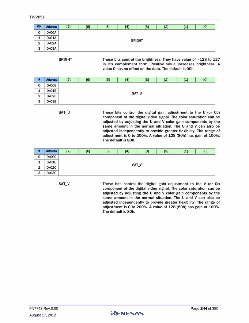
TW2851
FN7743 Rev.0.00 Page 244 of 380
August 17, 2012
VIN Address [7] [6] [5] [4] [3] [2] [1] [0]
0 0x00A
BRIGHT 1 0x01A
2 0x02A
3 0x03A
BRIGHT These bits control the brightness. They have value of –128 to 127
in 2's complement form. Positive value increases brightness. A
value 0 has no effect on the data. The default is 00h.
# Address [7] [6] [5] [4] [3] [2] [1] [0]
0 0x00B
SAT_U 1 0x01B
2 0x02B
3 0x03B
SAT_U These bits control the digital gain adjustment to the U (or Cb)
component of the digital video signal. The color saturation can be
adjusted by adjusting the U and V color gain components by the
same amount in the normal situation. The U and V can also be
adjusted independently to provide greater flexibility. The range of
adjustment is 0 to 200%. A value of 128 (80h) has gain of 100%.
The default is 80h.
# Address [7] [6] [5] [4] [3] [2] [1] [0]
0 0x00C
SAT_V 1 0x01C
2 0x02C
3 0x03C
SAT_V These bits control the digital gain adjustment to the V (or Cr)
component of the digital video signal. The color saturation can be
adjusted by adjusting the U and V color gain components by the
same amount in the normal situation. The U and V can also be
adjusted independently to provide greater flexibility. The range of
adjustment is 0 to 200%. A value of 128 (80h) has gain of 100%.
The default is 80h.

TW2851
FN7743 Rev.0.00 Page 245 of 380
August 17, 2012
# Address [7] [6] [5] [4] [3] [2] [1] [0]
0 0x00D
SF* PF* FF* KF* CSBAD* MCVSN* CSTRIPE* CTYPE2* 1 0x01D
2 0x02D
3 0x03D
* Read only bits
SF This bit is for internal use
PF This bit is for internal use
FF This bit is for internal use
KF This bit is for internal use
CSBAD 1 Macrovision color stripe detection may be un-reliable
MCVSN 1 Macrovision AGC pulse detected.
0 Not detected.
CSTRIPE 1 Macrovision color stripe protection burst detected.
0 Not detected.
CTYPE2 This bit is valid only when color stripe protection is detected, i.e. if
CSTRIPE=1,
1 Type 2 color stripe protection
0 Type 3 color stripe protection

TW2851
FN7743 Rev.0.00 Page 246 of 380
August 17, 2012
# Address [7] [6] [5] [4] [3] [2] [1] [0]
0 0x00E
DETSTUS*
STDNOW*
ATREG
STANDARD
1 0x01E
2 0x02E
3 0x03E
* Read only bits
DETSTUS 0 Idle
1 detection in progress
STDNOW Current standard invoked
0 NTSC(M)
1 PAL (B,D,G,H,I)
2 SECAM
3 NTSC4.43
4 PAL (M)
5 PAL (CN)
6 PAL 60
7 Not valid
ATREG 1 Disable the shadow registers
0 Enable VACTIVE and HDELAY shadow registers value
depending on STANDARD. (Default)
STANDARD Standard selection
0 NTSC(M)
1 PAL (B,D,G,H,I)
2 SECAM
3 NTSC4.43
4 PAL (M)
5 PAL (CN)
6 PAL 60
7 Auto detection (Default)

TW2851
FN7743 Rev.0.00 Page 247 of 380
August 17, 2012
# Address [7] [6] [5] [4] [3] [2] [1] [0]
0 0x00F
ATSTART PAL60EN PALCNEN PALMEN NTSC44EN SECAMEN PALBEN NTSCEN 1 0x01F
2 0x02F
3 0x03F
ATSTART 1 Writing 1 to this bit will manually initiate the auto format
detection process. This bit is a self-clearing bit
0 Manual initiation of auto format detection is done.
(Default)
PAL60EN 1 Enable recognition of PAL60 (Default)
0 Disable recognition
PALCNEN 1 Enable recognition of PAL (CN). (Default)
0 Disable recognition
PALMEN 1 Enable recognition of PAL (M). (Default)
0 Disable recognition
NTSC44EN 1 Enable recognition of NTSC 4.43. (Default)
0 Disable recognition
SECAMEN 1 Enable recognition of SECAM. (Default)
0 Disable recognition
PALBEN 1 Enable recognition of PAL (B,D,G,H,I). (Default)
0 Disable recognition
NTSCEN 1 Enable recognition of NTSC (M). (Default)
0 Disable recognition

TW2851
FN7743 Rev.0.00 Page 248 of 380
August 17, 2012
Address [7] [6] [5] [4] [3] [2] [1] [0]
0x045 0 0 VSMODE FLDPOL HSPOL VSPOL DECVSMODE DECFLDPOL
VSMODE Control the VS and field flag timing
0 VS and field flag is aligned with vertical sync of incoming
video (Default)
1 VS and field flag is aligned with HS
FLDPOL Select the FLD polarity
0 Odd field is high
1 Even field is high (Default)
HSPOL Select the HS polarity
0 Low for sync duration (Default)
1 High for sync duration
VSPOL Select the VS polarity
0 Low for sync duration (Default)
1 High for sync duration
DECVSMODE 0 Default
DECFLDPOL 0 Default

TW2851
FN7743 Rev.0.00 Page 249 of 380
August 17, 2012
Address [7] [6] [5] [4] [3] [2] [1] [0]
0x046 AGCEN4 AGCEN3 AGCEN2 AGCEN1 AGCGAIN4[8] AGCGAIN3[8] AGCGAIN2[8] AGCGAIN1[8]
0x047 AGCGAIN1[7:0]
0x048 AGCGAIN2[7:0]
0x049 AGCGAIN3[7:0]
0x04A AGCGAIN4[7:0]
AGCENn Select Video AGC loop function on VIN of channel n
0 AGC loop function enabled (recommended for most
application cases) (default).
1 AGC loop function disabled. Gain is set by AGCGAINn
AGCGAINn These registers control the AGC gain of channel n when AGC loop is
disabled. Default value is 0F0h.
Address [7] [6] [5] [4] [3] [2] [1] [0]
0x04B PD_BIAS V_ADC_SAVE 0 0 0 YFLEN
PD_BIAS 1 Power down the bias of all 4 VADC
0 Do not power down the bias
V_ADC_SAVE Power Saving Mode Selection.
0 Most Power Consuming
7 Most Power Saving
IREF 0 Internal current reference 1 for Video ADC (default)
1 Internal current reference increase 30% for Video ADC.
VREF 0 Internal voltage reference for Video ADC (default)
1 Internal voltage reference shut down for Video ADC
YFLEN Analog Video CH1/CH2/CH3/CH4 anti-alias filter control
1 Enable(default)
0 Disable
Address [7] [6] [5] [4] [3] [2] [1] [0]
0x04D TST_ADC_VD1 ADC_SEL1 0 0 0 0
TST_ADC_VD1 0 Default
ADC_SEL1 0 Default
Address [7] [6] [5] [4] [3] [2] [1] [0]
0x04E TST_ADC_VD2 ADC_SEL2 0 0 0 0
TST_ADC_VD2 0 Default
ADC_SEL2 0 Default

TW2851
FN7743 Rev.0.00 Page 250 of 380
August 17, 2012
Address [7] [6] [5] [4] [3] [2] [1] [0]
0x04F FRM YNR CLMD PSP
FRM Free run mode control
0 Auto(default)
2 Default to 60Hz
3 Default to 50Hz
YNR Y HF noise reduction
0 None(default)
1 Smallest
2 Small
3 Medium
CLMD Clamping mode control
0 Sync top
1 Auto(default)
2 Pedestal
3 N/A
PSP Slice level control
0 Low
1 Medium(default)
2 High
Address [7] [6] [5] [4] [3] [2] [1] [0]
0x050 HFLT2 HFLT1
0x051 HFLT4 HFLT3
HFLTn HFLTn controls the peaking function of channel n. Reserved for test
purpose.
Address [7] [6] [5] [4] [3] [2] [1] [0]
0x052 CTEST YCLEN 0 AFLTEN GTEST VLPF CKLY CKLC
CTEST Clamping control for debugging use. (Test purpose only)
(default 0)
YCLEN 1 Y channel clamp disabled (Test purpose only)
0 Enabled (default)
AFLTEN 1 Analog Audio input Anti-Aliasing Filter enabled (default)
0 Disabled
GTEST 1 Test (Test purpose only)
0 Normal operation (default)
VLPF Clamping filter control (default 0)
CKLY Clamping current control 1 (default 0)
CKLC Clamping current control 2 (default 0)

TW2851
FN7743 Rev.0.00 Page 251 of 380
August 17, 2012
Address [7] [6] [5] [4] [3] [2] [1] [0]
0x053 NT502 NT501
NT501 1 Force the Video Decoder 1 to a special NTSC 50 Hz
format
0 Do not force to NTSC 50 Hz format
NT502 1 Force the Video Decoder 2 to a special NTSC 50 Hz
format
0 Do not force to NTSC 50 Hz format
Address [7] [6] [5] [4] [3] [2] [1] [0]
0x054 NT504 NT503 DIV_RST DOUT_RST ACALEN AADC_SAVE
NT503 1 Force the Video Decoder 4 to a special NTSC 50 Hz
format
0 Do not force to NTSC 50 Hz format
NT504 1 Force the Video Decoder 4 to a special NTSC 50 Hz
format
0 Do not force to NTSC 50 Hz format
DIV_RST Audio ADC divider reset. This bit must be set to 0 again after reset.
DOUT_RST Audio ADC digital output reset for all channel. This bit must be
setup up to 0 again after reset.
ACALEN Audio ADC Calibration control. This be must be set up to 0 again
after enabled.
AADC_SAVE Audio ADC Power Saving Mode. 7 is most power saving.
Address [7] [6] [5] [4] [3] [2] [1] [0]
0x055 FLD* VAV*
FLD Status of the field flag for corresponding channel (Read only)
FLD[3:0] are FIELD ID for VIN3 to VIN0.
0 Odd field when FLDPOL (0x045) = 1
1 Even field when FLDPOL (0x045) = 1
VAV Status of the vertical active video signal for corresponding channel
(Read only). VAV[3:0] are Vertical Active Video Signal for VIN3 to
VIN0.
0 Vertical blanking time
1 Vertical active time

TW2851
FN7743 Rev.0.00 Page 252 of 380
August 17, 2012
Address [7] [6] [5] [4] [3] [2] [1] [0]
0x057 SHCOR ANA_SW4 ANA_SW3 ANA_SW2 ANA_SW1
SHCOR These bits provide coring function for the sharpness control
(default 3h)
ANA_SWn Control the analog input channel switch for VIN1 to VIN4 input
0 VIN_A channel is selected (default)
1 VIN_B channel is selected
Address [7] [6] [5] [4] [3] [2] [1] [0]
0x058 PBW DEM PALSW SET7 COMB HCOMP YCOMB PDLY
PBW 1 Wide Chroma BPF BW (Default)
0 Normal Chroma BPF BW
DEM Reserved (Default 1)
PALSW 1 PAL switch sensitivity low.
0 PAL switch sensitivity normal (Default)
SET7 1 The black level is 7.5 IRE above the blank level.
0 The black level is the same as the blank level (Default)
COMB 1 Adaptive comb filter for NTSC and PAL
(Recommended). This setting is not for SECAM (Default)
0 Notch filter. For SECAM, always set to 0.
HCOMP 1 Operation mode 1 (Recommended) (Default)
0 Mode 0
YCOMB 1 Bypass Comb filter when no burst presence
0 No bypass (Default)
PDLY 0 Enable PAL delay line (default)
1 Disable PAL delay line
Address [7] [6] [5] [4] [3] [2] [1] [0]
0x059 GMEN CKHY HSDLY
GMEN Reserved (Default 0)
CKHY Color killer hysteresis.
0 Fastest (Default)
1 Fast
2 Medium
3 Slow
HSDLY Reserved for test

TW2851
FN7743 Rev.0.00 Page 253 of 380
August 17, 2012
Address [7] [6] [5] [4] [3] [2] [1] [0]
0x05A CTCOR CCOR VCOR CIF
CTCOR These bits control the coring for CTI (Default 1h)
CCOR These bits control the low level coring function for the Cb/Cr output
(Default 0h)
VCOR These bits control the coring function of vertical peaking
(Default 1h)
CIF These bits control the IF compensation level.
0 None(default)
1 1.5dB
2 3dB
3 6dB
Address [7] [6] [5] [4] [3] [2] [1] [0]
0x05B CLPEND CLPST
CLPEND These 4 bits set the end time of the clamping pulse. Its value
should be larger than the value of CLPST (Default 5h)
CLPST These 4 bits set the start time of the clamping. It is referenced to
PCLAMP position. (Default 0h)
Address [7] [6] [5] [4] [3] [2] [1] [0]
0x05C NMGAIN WPGAIN FC27
NMGAIN These bits control the normal AGC loop maximum correction value
(Default 4h)
WPGAIN Peak AGC loop gain control (Default 1h)
FC27 1 Normal ITU-R656 operation (Default)
0 Squared Pixel mode for test purpose only
Address [7] [6] [5] [4] [3] [2] [1] [0]
0x05D PEAKWT
PEAKWT These bits control the white peak detection threshold. Setting ‘FF’
can disable this function (Default D8h)

TW2851
FN7743 Rev.0.00 Page 254 of 380
August 17, 2012
Address [7] [6] [5] [4] [3] [2] [1] [0]
0x05E CLMPLD CLMPL
CLMPLD 0 Clamping level is set by CLMPL
1 Clamping level preset at 60d (Default)
CLMPL These bits determine the clamping level of the Y channel (Default
3Ch)
Address [7] [6] [5] [4] [3] [2] [1] [0]
0x05F SYNCTD SYNCT
SYNCTD 0 Reference sync amplitude is set by SYNCT
1 Reference sync amplitude is preset to 38h (Default)
SYNCT These bits determine the standard sync pulse amplitude for AGC
reference (Default 38h)
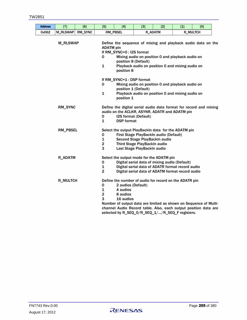
TW2851
FN7743 Rev.0.00 Page 255 of 380
August 17, 2012
Address [7] [6] [5] [4] [3] [2] [1] [0]
0x062 M_RLSWAP RM_SYNC RM_PBSEL R_ADATM R_MULTCH
M_RLSWAP Define the sequence of mixing and playback audio data on the
ADATM pin
If RM_SYNC=0 : I2S format
0 Mixing audio on position 0 and playback audio on
position 8 (Default)
1 Playback audio on position 0 and mixing audio on
position 8
If RM_SYNC=1 : DSP format
0 Mixing audio on position 0 and playback audio on
position 1 (Default)
1 Playback audio on position 0 and mixing audio on
position 1
RM_SYNC Define the digital serial audio data format for record and mixing
audio on the ACLKR, ASYNR, ADATR and ADATM pin
0 I2S format (Default)
1 DSP format
RM_PBSEL Select the output PlayBackIn data for the ADATM pin
0 First Stage PlayBackIn audio (Default)
1 Second Stage PlayBackIn audio
2 Third Stage PlayBackIn audio
3 Last Stage PlayBackIn audio
R_ADATM Select the output mode for the ADATM pin
0 Digital serial data of mixing audio (Default)
1 Digital serial data of ADATR format record audio
2 Digital serial data of ADATM format record audio
R_MULTCH Define the number of audio for record on the ADATR pin
0 2 audios (Default)
1 4 audios
2 8 audios
3 16 audios
Number of output data are limited as shown on Sequence of Multi-
channel Audio Record table. Also, each output position data are
selected by R_SEQ_0/R_SEQ_1/…/R_SEQ_F registers.

TW2851
FN7743 Rev.0.00 Page 256 of 380
August 17, 2012
Address [7] [6] [5] [4] [3] [2] [1] [0]
0x063 AAUTO_MUTE PBREFEN VRSTSEL FIRSTCNUM
AAUTO_MUTE 1 When input Analog data is less than ADET_TH level,
output PCM data will be set to 0. Audio DAC data input
is 0x200.
0 No effect
PBREFEN Audio ACKG Reference (refin) input select
0 ACKG has video VRST refin input selected by VRSTSEL
register (Default)
1 ACKG has audio ASYNP refin input
VRSTSEL Select VRST(V reset) signal on ACKG (Audio Clock Generator) refin
input .
0 VIN0 Video Decoder Path VRST (default)
1 VIN1 Video Decoder Path VRST
2 VIN2 Video Decoder Path VRST
3 VIN3 Video Decoder Path VRST
FIRSTCNUM Set up First Stage number on audio cascade mode connection.
Set up the value of (Cascade chip number-1). In 4 chips cascade
case, this value is 3h for ALINK mode. In single chip application
case, this doesn’t need to be set up.
0 (default)
Address [7] [6] [5] [4] [3] [2] [1] [0]
0x064 R_SEQ_1 R_SEQ_0
0x065 R_SEQ_3 R_SEQ_2
0x066 R_SEQ_5 R_SEQ_4
0x067 R_SEQ_7 R_SEQ_6
0x068 R_SEQ_9 R_SEQ_8
0x069 R_SEQ_B R_SEQ_A
0x06A R_SEQ_D R_SEQ_C
0x06B R_SEQ_F R_SEQ_E
R_SEQ Define the sequence of record audio on the ADATR pin.
Refer to Table 15 for the detail of the R_SEQ_0 ~ R_SEQ_F.
The default value of R_SEQ_0 is “0”, R_SEQ_1 is “1”, … and
R_SEQ_F is “F”.
0 AIN1
1 AIN2
: :
: :
14 AIN15
15 AIN16

TW2851
FN7743 Rev.0.00 Page 257 of 380
August 17, 2012
Address [7] [6] [5] [4] [3] [2] [1] [0]
0x06C ADACEN AADCEN PB_
MASTER PB_LRSEL PB_SYNC RM_8BIT ASYNROEN ACLKRMASTER
ADACEN Audio DAC Function mode
0 Audio DAC function disable (test purpose only)
1 Audio DAC function enable (Default)
AADCEN Audio ADC Function mode
0 Audio ADC function disable(test purpose only)
1 Audio ADC function enable (Default)
PB_MASTER Define the operation mode of the ACLKP and ASYNP pin for
playback.
0 All type I2S/DSP Slave mode (ACLKP and ASYNP is
input) (Default)
1 TW2851 type I2S/DSP Master mode (ACLKP and
ASYNP is output)
PB_LRSEL Select the channel for playback.
0 Left channel audio is used for playback input (Default)
1 Right channel audio is used for playback input
PB_SYNC Define the digital serial audio data format for playback audio on
the ACLKP, ASYNP and ADATP pin.
0 I2S format (Default)
1 DSP format
RM_8BIT Define output data format per one word unit on ADATR pin.
0 16bit one word unit output (Default)
1 8bit one word unit packed output
ASYNROEN Define input/output mode on the ASYNR pin.
1 ASYNR pin is input
0 ASYNR pin is output (Default)
ACLKRMASTER Define input/output mode on the ACLKR pin and set up audio
256xfs system processing
0 ACLKR pin is input. External 256xfs clock should be
connected to ACLKR pin. This function is single chip
Audio slave mode only.
1 ACLKR pin is output. Internal ACKG generates 256xfs
clock (Default)

TW2851
FN7743 Rev.0.00 Page 258 of 380
August 17, 2012
Address [7] [6] [5] [4] [3] [2] [1] [0]
0x06D LAWMD MIX_
DERATIO MIX_MUTE
LAWMD Select u-Law/A-Law/PCM/SB data output format on ADATR and
ADATM pin.
0 PCM output (default)
1 SB(Signed MSB bit in PCM data is inverted) output
2 u-Law output
3 A-Law output
MIX_DERATIO Disable the mixing ratio value for all audio.
0 Apply individual mixing ratio value for each audio
(default)
1 Apply nominal value for all audio commonly
MIX_MUTE[n] Enable the mute function for audio channel AINn when n is 0 to 3.
It effects only for mixing. When n = 4, it enable the mute function
of the playback audio input. It effects only for single chip or the last
stage chip
0 Normal
1 Muted (default)
Address [7] [6] [5] [4] [3] [2] [1] [0]
0x06E MIX_RATIO2 MIX_RATIO1
0x06F MIX_RATIO4 MIX_RATIO3
0x070 0 0 0 0 MIX_RATIOP
MIX_RATIOn Define the ratio values for audio mixing of channel AINn
MIX_RATIOP Define the ratio values for audio mixing of playback audio input
If MRATIOMD = 0 (default)
0 0.25
1 0.31
2 0.38
3 0.44
4 0.50
5 0.63
6 0.75
7 0.88
8 1.00 (default)
9 1.25
10 1.50
11 1.75
12 2.00
13 2.25
14 2.50
15 2.75
If MRATIONMD = 1, Mixing ratio is MIX_RATIOn / 64

TW2851
FN7743 Rev.0.00 Page 259 of 380
August 17, 2012
Address [7] [6] [5] [4] [3] [2] [1] [0]
0x071 V_ADC_CKPOL A_ADC_CKPOL A_DAC_CKPOL MIX_OUTSEL
V_ADC_CKPOL Test purpose only (Default 0)
A_ADC_CKPOL Test purpose only (Default 0)
A_DAC_CKPOL Test purpose only (Default 0)
MIX_OUTSEL Define the final audio output for analog and digital mixing out.
0 Select record audio of channel 1
1 Select record audio of channel 2
2 Select record audio of channel 3
3 Select record audio of channel 4
4 Select record audio of channel 5
5 Select record audio of channel 6
6 Select record audio of channel 7
7 Select record audio of channel 8
8 Select record audio of channel 9
9 Select record audio of channel 10
10 Select record audio of channel 11
11 Select record audio of channel 12
12 Select record audio of channel 13
13 Select record audio of channel 14
14 Select record audio of channel 15
15 Select record audio of channel 16
16 Select playback audio of the first stage chip
17 Select playback audio of the second stage chip
18 Select playback audio of the third stage chip
19 Select playback audio of the last stage chip
20 Select mixed audio (default)
21 Select record audio of channel AIN51
22 Select record audio of channel AIN52
23 Select record audio of channel AIN53
24 Select record audio of channel AIN54

TW2851
FN7743 Rev.0.00 Page 260 of 380
August 17, 2012
Address [7] [6] [5] [4] [3] [2] [1] [0]
0x072 AAMPMD ADET_FILT ADET_TH4[4] ADET_TH3[4] ADET_TH2[4] ADET_TH1[4]
0x073 ADET_TH2[3:0] ADET_TH1[3:0]
0x074 ADET_TH4[3:0] ADET_TH3[3:0]
AAMPMD Define the audio detection method.
0 Detect audio if absolute amplitude is greater than
threshold
1 Detect audio if differential amplitude is greater than
Threshold (default)
ADET_FILT Select the filter for audio detection (default 4h)
0 Wide LPF
: :
7 Narrow LPF
ADET_THn Define the threshold value for audio detection of AINn (Default Ah)
0 Low value
: :
31 High value
If fs = 8kHz Audio Clock setting mode, Registers
0x072 = 0xC0
0x073 = 0xAA
0x074 = 0xAA
are typical setting.
If fs=16kHz/32kHz/44.1kHz/48kHz Audio Clock setting mode,
Registers
0x072 = 0xE0
0x073 = 0xBB
0x074 = 0xBB
are typical setting.
Address [7] [6] [5] [4] [3] [2] [1] [0]
0x075 ACKI[7:0]
0x076 ACKI[15:8]
0x077 0 0 ACKI[21:16]
ACKI These bits control ACKI Clock Increment in ACKG block.
09B583h for fs = 8kHz is default
Address [7] [6] [5] [4] [3] [2] [1] [0]
0x078 ACKN[7:0]
0x079 ACKN[15:8]
0x07A 0 0 0 0 0 0 ACKN[17:16]
ACKN These bits control ACKN Clock Number in ACKG block..
000100h for Playback Slave-in lock is default.

TW2851
FN7743 Rev.0.00 Page 261 of 380
August 17, 2012
Address [7] [6] [5] [4] [3] [2] [1] [0]
0x07B 0 0 SDIV
SDIV These bits control SDIV Serial Clock Divider in ACKG block (Default
01h)
Address [7] [6] [5] [4] [3] [2] [1] [0]
0x07C 0 0 LRDIV
LRDIV These bits control LRDIV Left/Right Clock Divider in ACKG block
(Default 20h)
Address [7] [6] [5] [4] [3] [2] [1] [0]
0x07D APZ APG 0 ACPL SRPH LRPH
APZ These bits control Loop in ACKG block (Default 1)
APG These bits control Loop in ACKG block (Default 4h)
ACPL These bits control Loop closed/open in ACKG block
0 Loop closed
1 Loop open (recommended on typical application case)
(Default)
SRPH Reserved. These bits are not used in TW2851 chip.
LRPH Reserved. These bits are not used in TW2851 chip.
Address [7] [6] [5] [4] [3] [2] [1] [0]
0x0C0 BGNDEN BGNDCOL AUTO_BGND LIM_656 0
BGNDEN[n] Enable the background color for channel n for byte-interleave video
decoder output.
0 Background color is disabled (Default)
1 Background color is enabled
BGNDCOL Select the background color when BGNDEN = “1” or when
AUTO_BGND = “1” and Video Loss is detected
0 Blue color (Default)
1 Black color
AUTO_BGND Select the decoder background mode for byte-interleave video
decoder output.
0 Manual background mode (Default)
1 Automatic background mode when No-video is detected
LIM_656 Clamp the Y and C value in the video stream
0 Maximum of Y is 254, Minimum of Y is 1
Maximum of C is 254, Minimum of Y is 1
1 Maximum of Y is 235, Minimum of Y is 16
Maximum of Y is 240, Minimum of Y is 16

TW2851
FN7743 Rev.0.00 Page 262 of 380
August 17, 2012
Address [7] [6] [5] [4] [3] [2] [1] [0]
0x0C1 0 OUT_CHID SAV_CHID TST_EHAV_BLK 0 0 0 0
TST_EHAV_BLK Testing purpose only
1 Force the Y value to be 0 when HAV is high.
0 Normal Operation
OUT_CHID Enable the channel ID format in the horizontal blanking period of
Record Bypass byte interleaving BT 656 stream
0 Disable the channel ID format (default)
1 Enable the channel ID format
The lowest 4 bits of Y and C pixel value during horizontal blanking
is
Bit 3 Video Loss
Bit 2 Analog Mux A/B
Bit 1-0 Port ID
SAV_CHID Enable the channel ID format in the SAV/EAV header in Record
Bypass byte interleaving BT656 stream
0 Disable the channel ID format (default)
1 Enable the channel ID format
The SAV/EAV format is FF, 00, 00, XX
When SAV_CHID is enabled, the bits in XX is
Bit 7 Detect Video
Bit 1:0 Port ID
Address [7] [6] [5] [4] [3] [2] [1] [0]
0x0D0 AADC3OFS[9:8] AADC2OFS[9:8] AADC1OFS[9:8] AADC0OFS[9:8]
0x0D1 AADC0OFS[7:0]
0x0D2 AADC1OFS[7:0]
0x0D3 AADC2OFS[7:0]
0X0D4 AADC3OFS[7:0]
0x0D5 0 0 0 0 0 0 AADC4OFS[9:8]
0x0D6 AADC4OFS[7:0]
Digital ADC input data offset control. Digital ADC input data is adjusted by
ADJAADCn = AUDADCn + AADCnOFS
Where AUDADCn is 2’s formatted Analog Audio ADC output, and AADCnOFS is adjusted
offset value by 2’s format. All default 10bit data value is 3EFh.
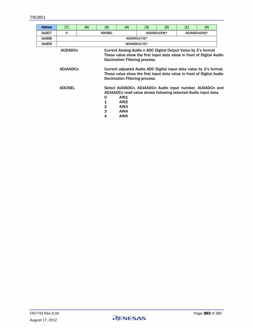
TW2851
FN7743 Rev.0.00 Page 263 of 380
August 17, 2012
Address [7] [6] [5] [4] [3] [2] [1] [0]
0x0D7 0 ADCISEL AUDADCn[9:8]* ADJAADCn[9:8]*
0x0D8 AUDADCn[7:0]*
0x0D9 ADJAADCn[7:0]*
AUDADCn Current Analog Audio n ADC Digital Output Value by 2’s format
` These value show the first input data value in front of Digital Audio
Decimation Filtering process.
ADJAADCn Current adjusted Audio ADC Digital input data value by 2’s format.
These value show the first input data value in front of Digital Audio
Decimation Filtering process.
ADCISEL Select AUDADCn, ADJAADCn Audio input number. AUDADCn and
ADJAADCn read value shows following selected Audio input data.
0 AIN1
1 AIN2
2 AIN3
3 AIN4
4 AIN5
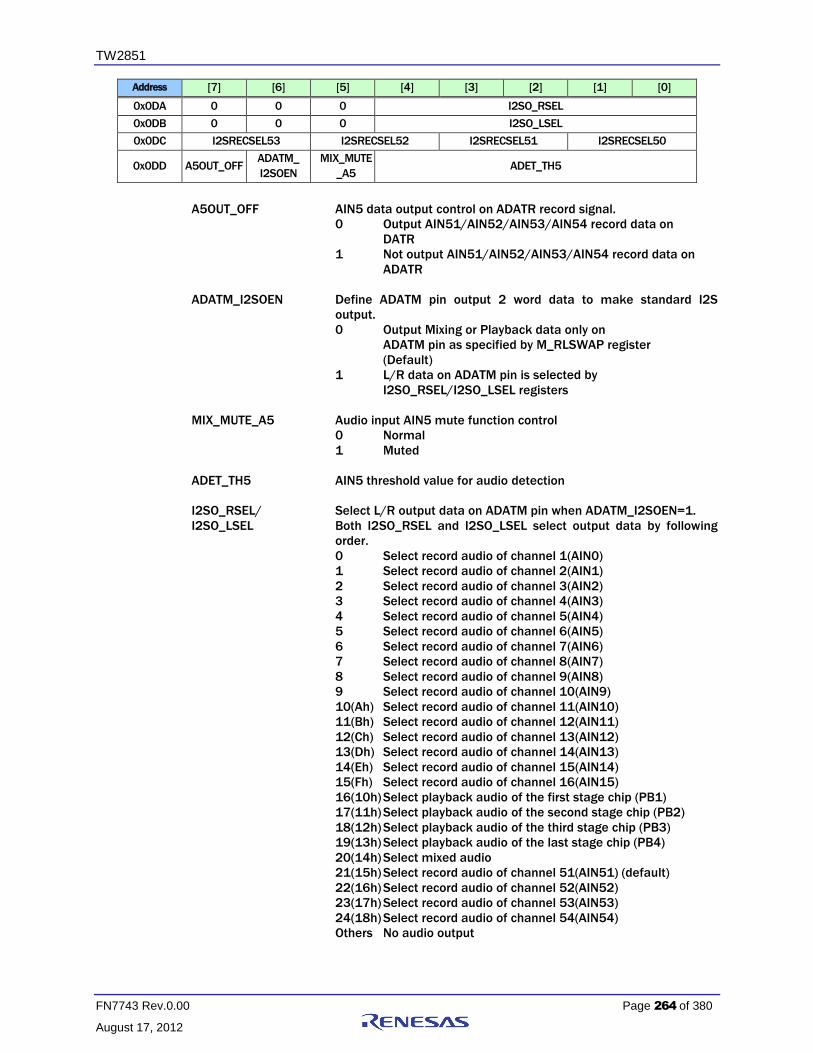
TW2851
FN7743 Rev.0.00 Page 264 of 380
August 17, 2012
Address [7] [6] [5] [4] [3] [2] [1] [0]
0x0DA 0 0 0 I2SO_RSEL
0x0DB 0 0 0 I2SO_LSEL
0x0DC I2SRECSEL53 I2SRECSEL52 I2SRECSEL51 I2SRECSEL50
0x0DD A5OUT_OFF ADATM_
I2SOEN
MIX_MUTE
_A5 ADET_TH5
A5OUT_OFF AIN5 data output control on ADATR record signal.
0 Output AIN51/AIN52/AIN53/AIN54 record data on
DATR
1 Not output AIN51/AIN52/AIN53/AIN54 record data on
ADATR
ADATM_I2SOEN Define ADATM pin output 2 word data to make standard I2S
output.
0 Output Mixing or Playback data only on
ADATM pin as specified by M_RLSWAP register
(Default)
1 L/R data on ADATM pin is selected by
I2SO_RSEL/I2SO_LSEL registers
MIX_MUTE_A5 Audio input AIN5 mute function control
0 Normal
1 Muted
ADET_TH5 AIN5 threshold value for audio detection
I2SO_RSEL/ Select L/R output data on ADATM pin when ADATM_I2SOEN=1.
I2SO_LSEL Both I2SO_RSEL and I2SO_LSEL select output data by following
order.
0 Select record audio of channel 1(AIN0)
1 Select record audio of channel 2(AIN1)
2 Select record audio of channel 3(AIN2)
3 Select record audio of channel 4(AIN3)
4 Select record audio of channel 5(AIN4)
5 Select record audio of channel 6(AIN5)
6 Select record audio of channel 7(AIN6)
7 Select record audio of channel 8(AIN7)
8 Select record audio of channel 9(AIN8)
9 Select record audio of channel 10(AIN9)
10(Ah) Select record audio of channel 11(AIN10)
11(Bh) Select record audio of channel 12(AIN11)
12(Ch) Select record audio of channel 13(AIN12)
13(Dh) Select record audio of channel 14(AIN13)
14(Eh) Select record audio of channel 15(AIN14)
15(Fh) Select record audio of channel 16(AIN15)
16(10h) Select playback audio of the first stage chip (PB1)
17(11h) Select playback audio of the second stage chip (PB2)
18(12h) Select playback audio of the third stage chip (PB3)
19(13h) Select playback audio of the last stage chip (PB4)
20(14h) Select mixed audio
21(15h) Select record audio of channel 51(AIN51) (default)
22(16h) Select record audio of channel 52(AIN52)
23(17h) Select record audio of channel 53(AIN53)
24(18h) Select record audio of channel 54(AIN54)
Others No audio output
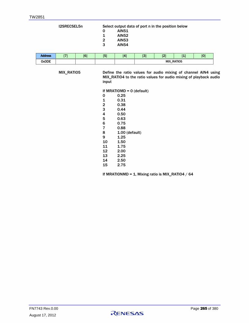
TW2851
FN7743 Rev.0.00 Page 265 of 380
August 17, 2012
I2SRECSEL5n Select output data of port n in the position below
0 AIN51
1 AIN52
2 AIN53
3 AIN54
Address [7] [6] [5] [4] [3] [2] [1] [0]
0x0DE MIX_RATIO5
MIX_RATIO5 Define the ratio values for audio mixing of channel AIN4 using
MIX_RATIO4 to the ratio values for audio mixing of playback audio
input
If MRATIOMD = 0 (default)
0 0.25
1 0.31
2 0.38
3 0.44
4 0.50
5 0.63
6 0.75
7 0.88
8 1.00 (default)
9 1.25
10 1.50
11 1.75
12 2.00
13 2.25
14 2.50
15 2.75
If MRATIONMD = 1, Mixing ratio is MIX_RATIO4 / 64
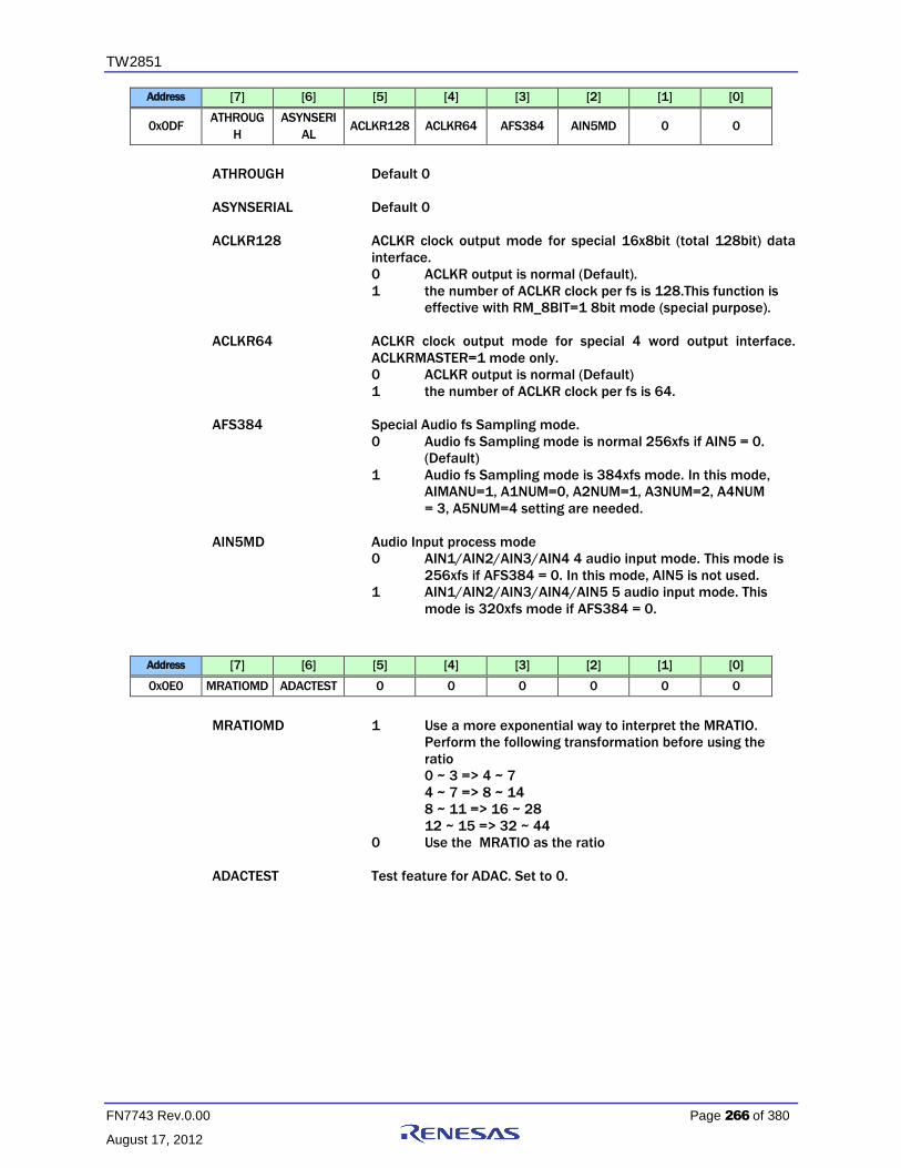
TW2851
FN7743 Rev.0.00 Page 266 of 380
August 17, 2012
Address [7] [6] [5] [4] [3] [2] [1] [0]
0x0DF ATHROUG
H
ASYNSERI
AL ACLKR128 ACLKR64 AFS384 AIN5MD 0 0
ATHROUGH Default 0
ASYNSERIAL Default 0
ACLKR128 ACLKR clock output mode for special 16x8bit (total 128bit) data
interface.
0 ACLKR output is normal (Default).
1 the number of ACLKR clock per fs is 128.This function is
effective with RM_8BIT=1 8bit mode (special purpose).
ACLKR64 ACLKR clock output mode for special 4 word output interface.
ACLKRMASTER=1 mode only.
0 ACLKR output is normal (Default)
1 the number of ACLKR clock per fs is 64.
AFS384 Special Audio fs Sampling mode.
0 Audio fs Sampling mode is normal 256xfs if AIN5 = 0.
(Default)
1 Audio fs Sampling mode is 384xfs mode. In this mode,
AIMANU=1, A1NUM=0, A2NUM=1, A3NUM=2, A4NUM
= 3, A5NUM=4 setting are needed.
AIN5MD Audio Input process mode
0 AIN1/AIN2/AIN3/AIN4 4 audio input mode. This mode is
256xfs if AFS384 = 0. In this mode, AIN5 is not used.
1 AIN1/AIN2/AIN3/AIN4/AIN5 5 audio input mode. This
mode is 320xfs mode if AFS384 = 0.
Address [7] [6] [5] [4] [3] [2] [1] [0]
0x0E0 MRATIOMD ADACTEST 0 0 0 0 0 0
MRATIOMD 1 Use a more exponential way to interpret the MRATIO.
Perform the following transformation before using the
ratio
0 ~ 3 => 4 ~ 7
4 ~ 7 => 8 ~ 14
8 ~ 11 => 16 ~ 28
12 ~ 15 => 32 ~ 44
0 Use the MRATIO as the ratio
ADACTEST Test feature for ADAC. Set to 0.

TW2851
FN7743 Rev.0.00 Page 267 of 380
August 17, 2012
Address [7] [6] [5] [4] [3] [2] [1] [0]
0x0E3 0 0 ACLKRPOL ACLKPPOL AFAUTO AFMD
ACLKRPOL ACLKR input signal polarity inverse.
0 Not inversed (Default)
1 Inversed
ACLKPPOL ACLKP input signal polarity inverse.
0 Not inversed (Default)
1 Inversed
AFAUTO ACKI[21:0] control automatic set up with AFMD registers
This mode is only effective when ACLKRMASTER=1
0 ACKI[21:0] registers set up ACKI control
1 ACKI control is automatically set up by AFMD register
values
AFMD AFAUTO control mode
0 8kHz setting (Default)
1 16kHz setting
2 32kHz setting
3 44.1kHz setting
4 48kHz setting

TW2851
FN7743 Rev.0.00 Page 268 of 380
August 17, 2012
Address [7] [6] [5] [4] [3] [2] [1] [0]
0x0E4 I2S8MODE MASCKMD PBINSWAP ASYNRDLY ASYNPDLY ADATPDLY INLAWMD
I2S8MODE 8bit I2S Record output mode.
0 L/R half length separated output (Default).
1 One continuous packed output equal to DSP output
format.
MASCKMD Audio Clock Master ACLKR output wave format.
0 High period is one 27MHz clock period (default).
1 Almost duty 50-50% clock output on ACLKR pin. If this
mode is selected, two times bigger number value need
to be set up on the ACKI register. If AFAUTO=1, ACKI
control is automatically set up even if MASCKMD=1.
PBINSWAP Playback ACLKP/ASYNP/ADATP input data MSB-LSB
swapping.
0 Not swapping
1 Swapping.
ASYNRDLY ASYNR input signal delay.
0 No delay
1 Add one 27MHz period delay in ASYNR signal input
ASYNPDLY ASYNP input signal delay.
0 no delay
1 add one 27MHz period delay in ASYNP signal input
ADATPDLY ADATP input data delay by one ACLKP clock.
0 No delay (Default).This is for I2S type 1T delay input
interface.
1 Add 1 ACLKP clock delay in ADATP input data. This is
for left-justified type 0T delay input interface.
INLAWMD Select u-Law/A-Law/PCM/SB data input format on ADATP pin.
0 PCM input (Default)
1 SB (Signed MSB bit in PCM data is inverted) input
2 u-Law input
3 A-Law input
Address [7] [6] [5] [4] [3] [2] [1] [0]
0x0E5 0 0 0 0 0 0 AINTPOFF A5DETENA
AINTPOFF Test feature for ADAC. Set to 0.
A5DETENA Enable state register updating and interrupt request of audio AIN5
detection for each input
0 Disable state register updating and interrupt request
1 Enable state register updating and interrupt request

TW2851
FN7743 Rev.0.00 Page 269 of 380
August 17, 2012
Address [7] [6] [5] [4] [3] [2] [1] [0]
0x0E7 HASYNC OFDLY DECOUTMD 0 0 0
HASYNC 1 The length of EAV to SAV is set up and fixed by HBLEN
register
0 The length of SAV to EAV is setup and fixed by
HACTIVE registers
OFDLY FIELD output delay
0h 0H line delay FIELD output (601 mode only)
1h~6h 1H ~ 6H line delay FIELD output
7h Reserved
DECOUTMD Default 1
Address [7] [6] [5] [4] [3] [2] [1] [0]
0x0E8 HBLEN
HBLEN These bits are effective when HASYNC bit is set to 1. These bits
setup the length of EAV to SAV code when HASYNC bit is 1. Normal
value is (Total pixel per line – HACTIVE) value.
NTSC/PAL-M(60Hz) 8Ah = 858 – 720
PAL/SECAM(50Hz) 90h = 864 – 720
If register 0x00E[3] (ATREG for CH1) is set to 0, this value changes
into 8Ah or 90h at audio video format detection initial time
automatically according to CH1 video detection status.
Address [7] [6] [5] [4] [3] [2] [1] [0]
0x0E9 CKLM YDLY 0 0 0 0
CKLM Color Killer mode.
0 Normal (Default)
1 Fast (For special application)
TDLY Luma delay fine adjustment. This 2's complement number
provides –4 to +3 unit delay control (Default 3h)
Address [7] [6] [5] [4] [3] [2] [1] [0]
0x0EA 0 0 ADECRST 0 VDEC4RST VDEC3RST VDEC2RST VDEC1RST
ADECRST A 1 written to this bit resets the audio portion to its default state
but all register content remains unchanged. This bit is self-cleared.
VDECnRST A 1 written to this bit resets the VINn path Video Decoder portion to
its default state but all register content remain unchanged. This bit
is self cleared.
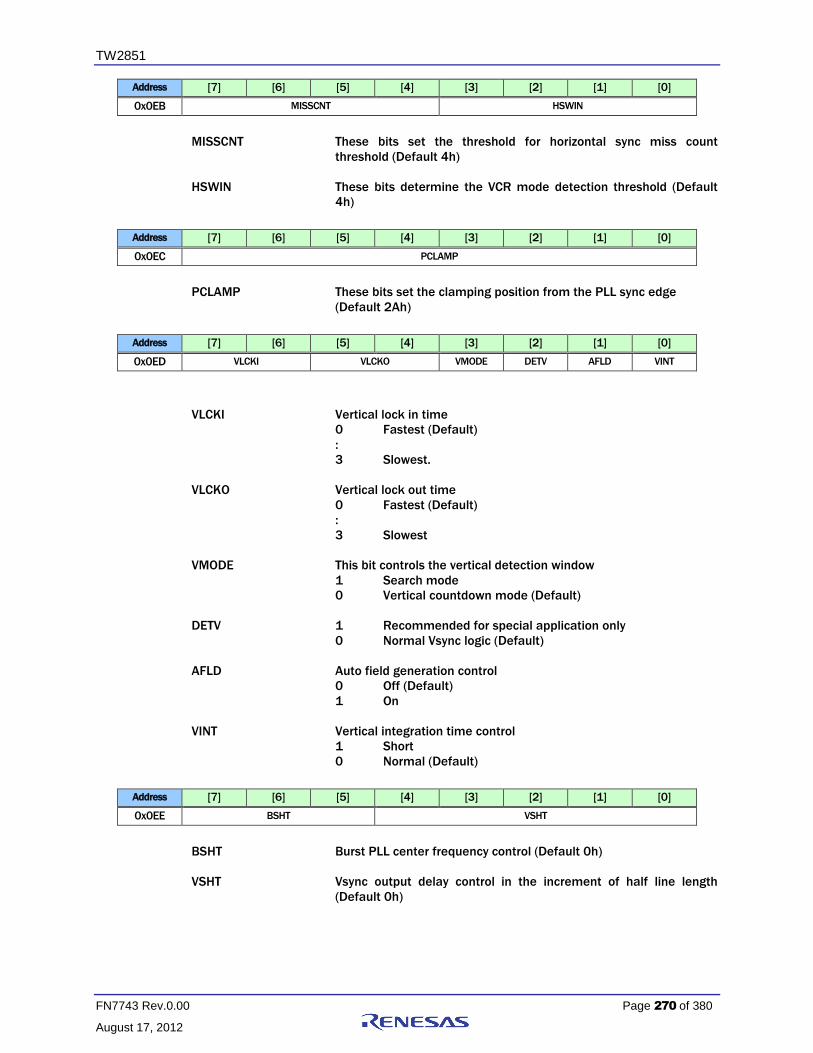
TW2851
FN7743 Rev.0.00 Page 270 of 380
August 17, 2012
Address [7] [6] [5] [4] [3] [2] [1] [0]
0x0EB MISSCNT HSWIN
MISSCNT These bits set the threshold for horizontal sync miss count
threshold (Default 4h)
HSWIN These bits determine the VCR mode detection threshold (Default
4h)
Address [7] [6] [5] [4] [3] [2] [1] [0]
0x0EC PCLAMP
PCLAMP These bits set the clamping position from the PLL sync edge
(Default 2Ah)
Address [7] [6] [5] [4] [3] [2] [1] [0]
0x0ED VLCKI VLCKO VMODE DETV AFLD VINT
VLCKI Vertical lock in time
0 Fastest (Default)
:
3 Slowest.
VLCKO Vertical lock out time
0 Fastest (Default)
:
3 Slowest
VMODE This bit controls the vertical detection window
1 Search mode
0 Vertical countdown mode (Default)
DETV 1 Recommended for special application only
0 Normal Vsync logic (Default)
AFLD Auto field generation control
0 Off (Default)
1 On
VINT Vertical integration time control
1 Short
0 Normal (Default)
Address [7] [6] [5] [4] [3] [2] [1] [0]
0x0EE BSHT VSHT
BSHT Burst PLL center frequency control (Default 0h)
VSHT Vsync output delay control in the increment of half line length
(Default 0h)

TW2851
FN7743 Rev.0.00 Page 271 of 380
August 17, 2012
Address [7] [6] [5] [4] [3] [2] [1] [0]
0x0EF CKILLMAX CKILLMIN
CKILLMAX These bits control the amount of color killer hysteresis. The
hysteresis amount is proportional to the value (Default 1h)
CKILLMIN These bits control the color killer threshold. Larger value gives
lower killer level (Default 28h)
Address [7] [6] [5] [4] [3] [2] [1] [0]
0x0F0 COMBMD HTL VTL
COMBMD 0 Adaptive mode (Default)
1 Fixed comb
HTL Adaptive Comb filter threshold control 1 (Default 4h)
VTL Adaptive Comb filter threshold control 2 (Default Ch)
Address [7] [6] [5] [4] [3] [2] [1] [0]
0x0F1 HPLC EVCNT PALC SDET 0 BYPASS 0 0
HPLC Reserved for internal use (Default 0)
EVCNT 1 Even field counter in special mode
0 Normal operation (Default)
PALC Reserved for future use (Default 0)
SDET ID detection sensitivity. A '1' is recommended (Default 1)
BYPASS It controls the standard detection and should be set to ‘1’ in
normal use (Default 1)

TW2851
FN7743 Rev.0.00 Page 272 of 380
August 17, 2012
Address [7] [6] [5] [4] [3] [2] [1] [0]
0x0F2 HPM ACCT SPM CBW
HPM Horizontal PLL acquisition time.
0 Normal
1 Auto2
2 Auto1 (Default)
3 Fast
ACCT ACC time constant
0 No ACC
1 Slow
2 Medium (Default)
3 Fast
SPM Burst PLL control
0 Slowest
1 Slow (Default)
2 Fast
3 Fastest
CBW Chroma low pass filter bandwidth control. Refer to filter curves
(Default 1)

TW2851
FN7743 Rev.0.00 Page 273 of 380
August 17, 2012
Address [7] [6] [5] [4] [3] [2] [1] [0]
0x0F3 NKILL PKILL SKILL CBAL FCS LCS CCS BST
NKILL 1 Enable noisy signal color killer function in NTSC mode
(Default)
0 Disabled
PKILL 1 Enable automatic noisy color killer function in PAL mode
(Default)
0 Disabled
SKILL 1 Enable automatic noisy color killer function in SECAM
Mode (Default)
0 Disabled
CBAL 0 Normal output (Default)
1 Special output mode.
FCS 1 Force decoder output value determined by CCS
0 Disabled (Default)
LCS 1 Enable pre-determined output value indicated by CCS
when video loss is detected
0 Disabled (Default)
CCS When FCS is set high or video loss condition is detected when LCS
is set high, one of two colors display can be selected.
1 Blue color
0 Black (Default)
BST 1 Enable blue stretch
0 Disabled (Default)
Address [7] [6] [5] [4] [3] [2] [1] [0]
0x0F4 0 0 MONITOR
0x0F5 HREF*
These registers are for test purpose only. The MONITOR is used to select the HREF status of
a certain video decoder port in Reg0x0F5 HREF
MONITOR Value Select video decoder port for register 0x0F5
00h VIN0 Video Decoder Path HREF[9:2] value
10h VIN1 Video Decoder Path HREF[9:2] value
20h VIN2 Video Decoder Path HREF[9:2] value
30h VIN3 Video Decoder Path HREF[9:2] value
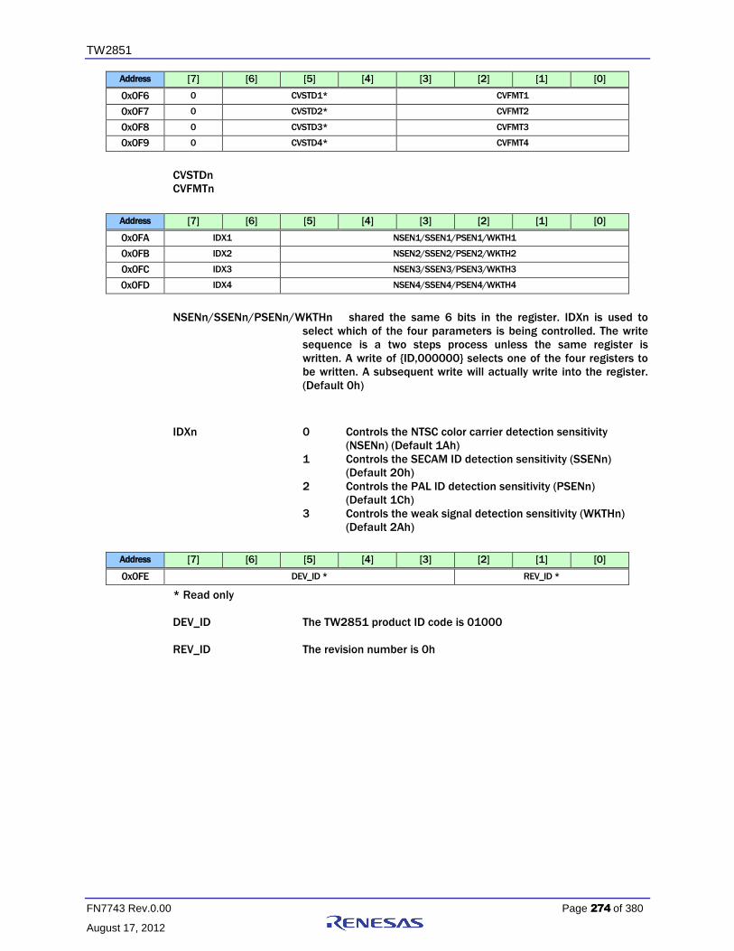
TW2851
FN7743 Rev.0.00 Page 274 of 380
August 17, 2012
Address [7] [6] [5] [4] [3] [2] [1] [0]
0x0F6 0 CVSTD1* CVFMT1
0x0F7 0 CVSTD2* CVFMT2
0x0F8 0 CVSTD3* CVFMT3
0x0F9 0 CVSTD4* CVFMT4
CVSTDn
CVFMTn
Address [7] [6] [5] [4] [3] [2] [1] [0]
0x0FA IDX1 NSEN1/SSEN1/PSEN1/WKTH1
0x0FB IDX2 NSEN2/SSEN2/PSEN2/WKTH2
0x0FC IDX3 NSEN3/SSEN3/PSEN3/WKTH3
0x0FD IDX4 NSEN4/SSEN4/PSEN4/WKTH4
NSENn/SSENn/PSENn/WKTHn shared the same 6 bits in the register. IDXn is used to
select which of the four parameters is being controlled. The write
sequence is a two steps process unless the same register is
written. A write of {ID,000000} selects one of the four registers to
be written. A subsequent write will actually write into the register.
(Default 0h)
IDXn 0 Controls the NTSC color carrier detection sensitivity
(NSENn) (Default 1Ah)
1 Controls the SECAM ID detection sensitivity (SSENn)
(Default 20h)
2 Controls the PAL ID detection sensitivity (PSENn)
(Default 1Ch)
3 Controls the weak signal detection sensitivity (WKTHn)
(Default 2Ah)
Address [7] [6] [5] [4] [3] [2] [1] [0]
0x0FE DEV_ID * REV_ID *
* Read only
DEV_ID The TW2851 product ID code is 01000
REV_ID The revision number is 0h

TW2851
FN7743 Rev.0.00 Page 275 of 380
August 17, 2012
Page 1: 0x100 ~ 0x1FE
Address [7] [6] [5] [4] [3] [2] [1] [0]
0x100 0 0 LIM_PB
_656
656_PB_EC
_BYPASS PB_CH_NO_VIDEO*
* Read only
LIM_PB_656 Specify the Clamping mode for PB input data at BT 656 mode
1 maximum 235, minimum 16
0 maximum 254, minimum 1
656_PB_EC_BYPASS Bypass the error correction of BT 656
1 Bypass error correction
0 Do not bypass error correction when the parity check is
wrong
PB_CH_NO_VIDEO[n] NO_VIDEO Status of Playback channel n (Read Only)
Address [7] [6] [5] [4] [3] [2] [1] [0]
0x101 PB_PORT_SEL3* PB_PORT_SEL2* PB_PORT_SEL1* PB_PORT_SEL0*
* Read only
PB_PORT_SELn The playback channel n mux selection of the physical playback
input port number (read only)
0 Channel n has input from Playback port 0
1 Channel n has input from Playback port 1
2 Channel n has input from Playback port 2
3 Channel n has input from Playback port 3

TW2851
FN7743 Rev.0.00 Page 276 of 380
August 17, 2012
Address [7] [6] [5] [4] [3] [2] [1] [0]
0x102 PB1_VS_
POL
PB1_HS_
POL PB1_TYPE
PB0_
WIDTH
PB0_VS_
POL
PB0_HS_
POL PB0_TYPE
PB1_VS_POL Playback Port 1 VSYNC signal polarity control
1 Reverse the polarity
0 Do not reverse the polarity
PB1_HS_POL Playback Port 1 HSYNC signal polarity control
1 Reverse the polarity
0 Do not reverse the polarity
PB1_TYPE Playback Port Type Control 1 – Refer to Table 3 for PB1_TYPE
setting with associated with PB0_TYPE
0 BT 656 mode
1 BT 601 mode
PB0_WIDTH Playback Port 0 Data Width when used as component input mode
(PB0_TYPE == 2’b11)
1 24 bits (R/V at PB2[7:0], G/Y at PB1[7:0], B/V at PB0[7:0])
0 16 bit mode (R/V at {PB1[1:0], PB0[7:5]}, G/Y at PB1[7:2],
B/V at PB0[4:0])
PB0_VS_POL Playback Port 0 VSYNC signal polarity control
1 Reverse the polarity
0 Do not reverse the polarity
PB0_HS_POL Playback Port 0 HSYNC signal polarity control
1 Reverse the polarity
0 Do not reverse the polarity
PB0_TYPE Playback Port Type Control 0 – Refer to Table 3 for PB0_TYPE
setting associated with PB1_TYPE
0 BT 656
1 BT 601
2 BT 1120
3 Component (RGB/YUV) input

TW2851
FN7743 Rev.0.00 Page 277 of 380
August 17, 2012
Address [7] [6] [5] [4] [3] [2] [1] [0]
0x103 PB0_PROG PB0_RGB PB_FLD_DET_MD PB_FLD_POL
PB0_PROG Port PB0 input Progressive
1 Port PB0 input is forced to progressive
0 Port PB0 input is interlaced
PB0_RGB 1 Input is in RGB format
0 Input is in YUV format
PB_FLD_DET_MODE[m]
LD Detection Mode when input port is 601 format for Port m
1 Field ID is derived by sample the HSYNC signal at the
leading edge of VSYNC
0 Field ID is derived by checking the distance between the
leading edge of HSYNC and VSYNC. If the distance is
larger than the VS_HS_LAG_TH specified in register
0x104 or 0x105, then this video field is an odd field.
Otherwise it is an even field.
PB_FLD_POL[m] Field Polarity Control for port m
1 Reverse the input field polarity
0 Do not reverse the input field polarity
Address [7] [6] [5] [4] [3] [2] [1] [0]
0x104 PB0_VS_HS_LAG_TH
0x105 PB1_VS_HS_LAG_TH
PB_VS_HS_LAG_TH Use the VS to HS distance to determine the field ID. When this
distance is larger than this threshold, the current video field is an
odd field (field ID = 1’b0). Else it is even field (field ID = 1’b1). Used
8’hFF when PB_FLD_DET_MODE in 0x103 is set to 0.
Address [7] [6] [5] [4] [3] [2] [1] [0]
0x106 PB0_HA_ST[7:0]
0x107 PB0_HA_LENGTH[7:0]
0x108 0 PB0_HA_LENGTH[10:8] 0 PB0_HA_ST[10:8]
PB0_HA_ST Specify the starting pixel of each line if PB port 0 is in BT 601
mode
PB0_HA_LEN Specify the horizontal active length if PB port 0 is in BT 601 mode

TW2851
FN7743 Rev.0.00 Page 278 of 380
August 17, 2012
Address [7] [6] [5] [4] [3] [2] [1] [0]
0x109 PB0_VA1_ST[7:0]
0x10A PB0_VA2_ST[7:0]
0x10B PB0_VA_LEN[7:0]
0x10C 0 0 PB0_VA_LEN[9:8] PB0_VA2_ST[9:8] PB0_VA1_ST[9:8]
PB0_VAx_ST Specify the starting line if PB port 0 is in BT 601 mode
PB0_VA1_ST: The starting line of even field
PB0_VA2_ST: The starting line of odd field
PB0_VA_LEN Specify the vertical active length if PB port 0 is in BT 601 mode
Address [7] [6] [5] [4] [3] [2] [1] [0]
0x10D PB1_HA_ST[7:0]
0x10E PB1_HA_LEN[7:0]
0x10F 0 PB1_HA_LEN[10:8] 0 PB1_HA_ST[10:8]
PB1_HA_ST Specify the starting pixel of each line if PB port 1 is in BT 601
mode
PB1_HA_LEN Specify the horizontal active length if PB port 1 is in BT 601 mode
Address [7] [6] [5] [4] [3] [2] [1] [0]
0x110 PB1_VA1_ST[7:0]
0x111 PB1_VA2_ST[7:0]
0x112 PB1_VA_LEN[7:0]
0x113 0 0 PB1_VA_LEN[9:8] PB1_VA2_ST[9:8] PB1_VA1_ST[9:8]
PB1_VAx_ST Specify the starting line if PB port 1 is in BT 601 mode
PB1_VA1_ST: The starting line of even field
PB1_VA2_ST: The starting line of odd field
PB1_VA_LEN Specify the vertical active length if PB port1 is in BT 601 mode
Address [7] [6] [5] [4] [3] [2] [1] [0]
0x120 PB0_MAN_STRB_EN PB0_MAN_PIC_TYPE
0x130 PB1_MAN_STRB_EN PB1_MAN_PIC_TYPE
0x140 PB2_MAN_STRB_EN PB2_MAN_PIC_TYPE
0x150 PB3_MAN_STRB_EN PB3_MAN_PIC_TYPE
PBm_MAN_STRB_EN Enable manual strobe mode for PB port m
1 Enable
0 Disable
PBm_MAN_PIC_TYPE Specify the picture type used in manual strobe mode for PB port m

TW2851
FN7743 Rev.0.00 Page 279 of 380
August 17, 2012
Address [7] [6] [5] [4] [3] [2] [1] [0]
0x121 PB0_MAN_CH1_ID PB0_MAN_CH0_ID
0x122 PB0_MAN_CH3_ID PB0_MAN_CH2_ID
0x131 PB1_MAN_CH1_ID PB1_MAN_CH0_ID
0x132 PB1_MAN_CH3_ID PB1_MAN_CH2_ID
0x141 PB2_MAN_CH1_ID PB2_MAN_CH0_ID
0x142 PB2_MAN_CH3_ID PB2_MAN_CH2_ID
0x151 PB3_MAN_CH1_ID PB3_MAN_CH0_ID
0x152 PB3_MAN_CH3_ID PB3_MAN_CH2_ID
PBm_MAN_CHn_ID Specify the channel ID to be used at PB port m channel n in
Manual Strobe mode
PBm_MAN_CHn_ID[3:2] chip ID
PBm_MAN_CHn_ID[1:0] channel ID
Address [7] [6] [5] [4] [3] [2] [1] [0]
0x123 0 PB0_AUTO_STRB_EN PB0_FORCE_LIVE PB0_MAN_STRB_FLD PB0_MAN_ANA
0x133 0 PB1_AUTO_STRB_EN PB1_FORCE_LIVE PB1_MAN_STRB_FLD PB1_MAN_ANA
0x143 0 PB2_FORCE_LIVE PB2_MAN_STRB_FLD PB2_MAN_ANA
0x153 0 PB3_FORCE_LIVE PB3_MAN_STRB_FLD PB3_MAN_ANA
PBm_AUTO_STRB_EN
Enable playback port m automatic strobe using the channel ID
embedded in the VBI. Only PB0 and PB1 has channel ID decoder.
PB2 and PB3 do not support audio CHID.
1 Enable to use the channel ID embedded in the VBI to
strobe. In this mode, the Strobe signal is sent out automatically
without CPU issuing a strobe signal.
0 Disable: Use the channel ID specified by the register
0x120 ~ 0x122, 0x130 ~ 0x132, 0x140 ~0x142, 0x150 ~
0x152 to strobe.
PBm_FORCE_LIVE Force the playback to strobe on whatever input video stream.
1 When this bit is set to 1, the strobe is always sent out. It
will behave like a LIVE input. When this mode is on, the
PBm_MAN_PIC_TYPE has to be set to 0x01.
0 When this bit is set to 0, the strobe will be sent out only if
there is a match if PB_CHNUM with the channel ID from
the VBI, or the channel ID specified in the registers in
0x120 ~0x122, 0x130 ~ 0x132, 0x140 ~ 0x142, 0x150 ~
0x152.
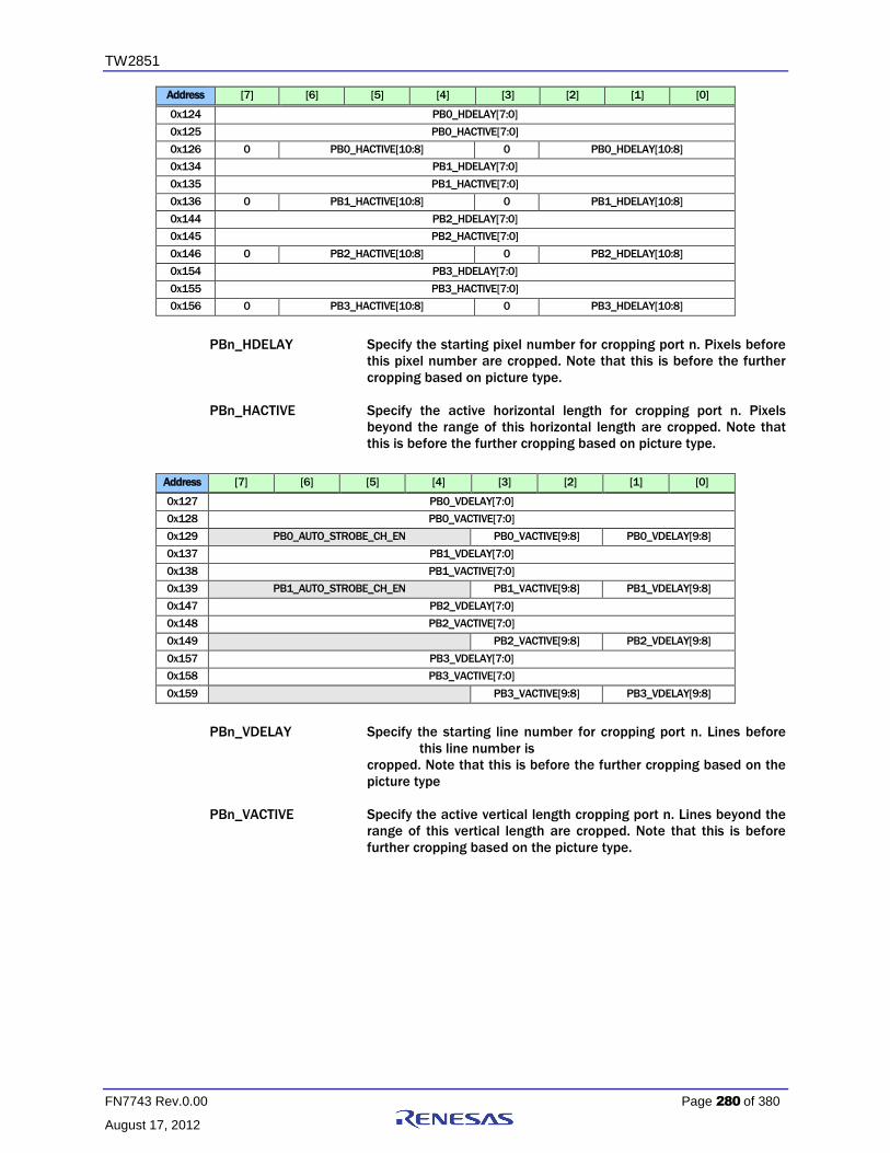
TW2851
FN7743 Rev.0.00 Page 280 of 380
August 17, 2012
Address [7] [6] [5] [4] [3] [2] [1] [0]
0x124 PB0_HDELAY[7:0]
0x125 PB0_HACTIVE[7:0]
0x126 0 PB0_HACTIVE[10:8] 0 PB0_HDELAY[10:8]
0x134 PB1_HDELAY[7:0]
0x135 PB1_HACTIVE[7:0]
0x136 0 PB1_HACTIVE[10:8] 0 PB1_HDELAY[10:8]
0x144 PB2_HDELAY[7:0]
0x145 PB2_HACTIVE[7:0]
0x146 0 PB2_HACTIVE[10:8] 0 PB2_HDELAY[10:8]
0x154 PB3_HDELAY[7:0]
0x155 PB3_HACTIVE[7:0]
0x156 0 PB3_HACTIVE[10:8] 0 PB3_HDELAY[10:8]
PBn_HDELAY Specify the starting pixel number for cropping port n. Pixels before
this pixel number are cropped. Note that this is before the further
cropping based on picture type.
PBn_HACTIVE Specify the active horizontal length for cropping port n. Pixels
beyond the range of this horizontal length are cropped. Note that
this is before the further cropping based on picture type.
Address [7] [6] [5] [4] [3] [2] [1] [0]
0x127 PB0_VDELAY[7:0]
0x128 PB0_VACTIVE[7:0]
0x129 PB0_AUTO_STROBE_CH_EN PB0_VACTIVE[9:8] PB0_VDELAY[9:8]
0x137 PB1_VDELAY[7:0]
0x138 PB1_VACTIVE[7:0]
0x139 PB1_AUTO_STROBE_CH_EN PB1_VACTIVE[9:8] PB1_VDELAY[9:8]
0x147 PB2_VDELAY[7:0]
0x148 PB2_VACTIVE[7:0]
0x149 PB2_VACTIVE[9:8] PB2_VDELAY[9:8]
0x157 PB3_VDELAY[7:0]
0x158 PB3_VACTIVE[7:0]
0x159 PB3_VACTIVE[9:8] PB3_VDELAY[9:8]
PBn_VDELAY Specify the starting line number for cropping port n. Lines before
this line number is
cropped. Note that this is before the further cropping based on the
picture type
PBn_VACTIVE Specify the active vertical length cropping port n. Lines beyond the
range of this vertical length are cropped. Note that this is before
further cropping based on the picture type.

TW2851
FN7743 Rev.0.00 Page 281 of 380
August 17, 2012
Address [7] [6] [5] [4] [3] [2] [1] [0]
0x129 PB0_AUTO_STROBE_CH_EN PB0_VACTIVE[9:8] PB0_VDELAY[9:8]
0x139 PB1_AUTO_STROBE_CH_EN PB1_VACTIVE[9:8] PB1_VDELAY[9:8]
0x149 PB2_VACTIVE[9:8] PB2_VDELAY[9:8]
0x159 PB3_VACTIVE[9:8] PB3_VDELAY[9:8]
PBn_AUTO_STROBE_CH_EN[m]
Specify whether to turn on the auto strobe for port n, on channels
m. Only PB0 and PB1 have channel ID decoder. PB2 and PB3 do
not support audio CHID.
Address [7] [6] [5] [4] [3] [2] [1] [0]
0x12A 0 PB0_CHID_FLD_OS PB0_DID_EN PB0_AID_EN PB0_FLT_EN PB0_RIC_EN PB0_AUTO_CHID_DET
0x13A 0 PB1_CHID_FLD_OS PB1_DID_EN PB1_AID_EN PB1_FLT_EN PB1_RIC_EN PB1_AUTO_CHID_DET
PBm_CHID_FLD_OS The PB port m CHID line offset of even field relative to odd field.
2 One line more than odd field
1 Same offset as odd field
0 One line less than odd field
PBm_DID_EN Enable digital channel ID detection for the PB port m
1 Turn on digital channel ID decoding
0 Turn off digital channel ID decoding
PBm_AID_EN Enable the Analog channel ID detection for PB port m
1 Turn on analog channel ID detection
0 Turn off analog channel ID detection
PBm_RIC_EN Select the run-in clock mode for analog channel ID
1 Run-in clock mode
0 No run-in clock mode
PBm_FLT_EN Select the LPF filter mode for playback input
0 Bypass mode
1 Enable the LPF filter
PBm_AUTO_CHID_DET Select the detection mode of Analog channel ID for playback input
port m
0 Manual detection mode for Analog channel ID
1 Automatic detection mode for Analog channel ID
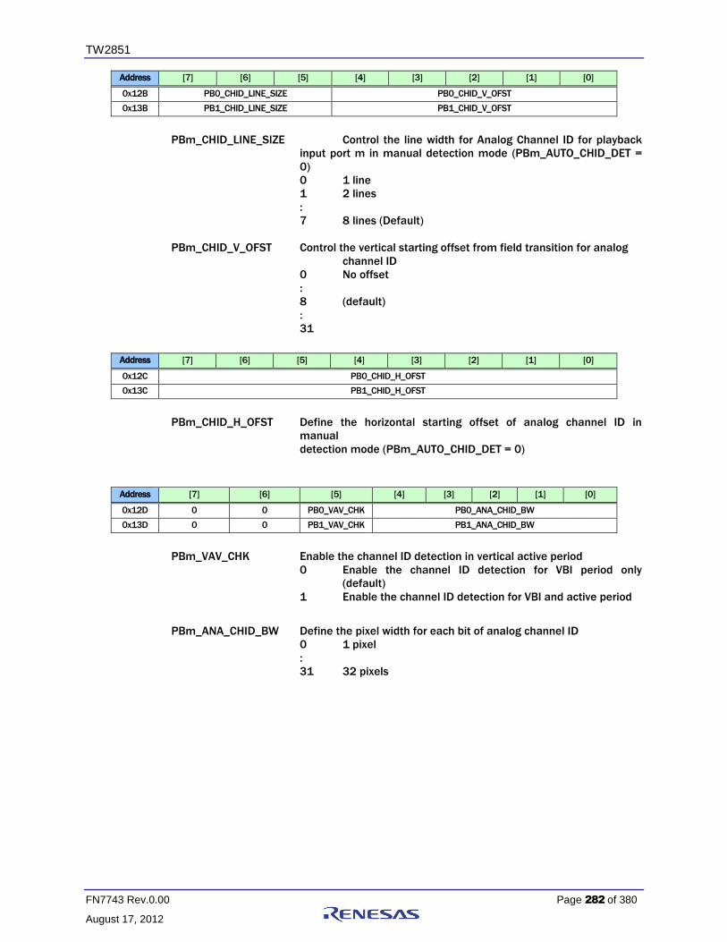
TW2851
FN7743 Rev.0.00 Page 282 of 380
August 17, 2012
Address [7] [6] [5] [4] [3] [2] [1] [0]
0x12B PB0_CHID_LINE_SIZE PB0_CHID_V_OFST
0x13B PB1_CHID_LINE_SIZE PB1_CHID_V_OFST
PBm_CHID_LINE_SIZE Control the line width for Analog Channel ID for playback
input port m in manual detection mode (PBm_AUTO_CHID_DET =
0)
0 1 line
1 2 lines
:
7 8 lines (Default)
PBm_CHID_V_OFST Control the vertical starting offset from field transition for analog
channel ID
0 No offset
:
8 (default)
:
31
Address [7] [6] [5] [4] [3] [2] [1] [0]
0x12C PB0_CHID_H_OFST
0x13C PB1_CHID_H_OFST
PBm_CHID_H_OFST Define the horizontal starting offset of analog channel ID in
manual
detection mode (PBm_AUTO_CHID_DET = 0)
Address [7] [6] [5] [4] [3] [2] [1] [0]
0x12D 0 0 PB0_VAV_CHK PB0_ANA_CHID_BW
0x13D 0 0 PB1_VAV_CHK PB1_ANA_CHID_BW
PBm_VAV_CHK Enable the channel ID detection in vertical active period
0 Enable the channel ID detection for VBI period only
(default)
1 Enable the channel ID detection for VBI and active period
PBm_ANA_CHID_BW Define the pixel width for each bit of analog channel ID
0 1 pixel
:
31 32 pixels

TW2851
FN7743 Rev.0.00 Page 283 of 380
August 17, 2012
Address [7] [6] [5] [4] [3] [2] [1] [0]
0x12E PB0_CHID_MID_VAL
0x13E PB1_CHID_MID_VAL
PBm_CHID_MID_VAL Define the slicer threshold level to detect bit “0” or bit “1” from
analog channel ID (default 128)
Address [7] [6] [5] [4] [3] [2] [1] [0]
0x15F 0 0 0 0 0 0 PB_NOVID_MD
PB_NOVID_MD Select the No-Video flag generation mode
0 Faster
1 Fast
2 Slow
3 Slower (default)
Address [7] [6] [5] [4] [3] [2] [1] [0]
0x160 0 PB_STOP0 PB_HSCL_BYP0 PB_ANA0 PB_CHNUM0
0x170 0 PB_STOP1 PB_HSCL_BYP1 PB_ANA1 PB_CHNUM1
0x180 0 0 PB_HSCL_BYP2 PB_ANA2 PB_CHNUM2
0x190 0 0 PB_HSCL_BYP3 PB_ANA3 PB_CHNUM3
PB_STOPn Disable the auto strobe operation for playback channel n
0 Normal Operation (default)
1 Stop the auto strobe operation for playback channel n
PB_ HSCL_BYPn Bypass the horizontal scaler for playback channel n
0 Normal operation
1 Bypass the horizontal scaler
PB_ANAn The analog input selection of channel n
0 Select VINA
1 Select VINB
PB_CHNUMn The playback channel ID selection
PB_CHNUMn[3:2] CHIP ID
PB_CHNUMn[1:0] Port ID
Address [7] [6] [5] [4] [3] [2] [1] [0]
0x161 PB_2X_EN0 PB_FLD_POL0
0x171 PB_2X_EN1 PB_FLD_POL1
0x181 PB_2X_EN2 PB_FLD_POL2
0x191 PB_2X_EN3 PB_FLD_POL3
PB_2X_ENn Scale up 2X horizontally for PB channel n
PB_FLD_POLn Reverse the field signal polarity of channel n

TW2851
FN7743 Rev.0.00 Page 284 of 380
August 17, 2012
Address [7] [6] [5] [4] [3] [2] [1] [0]
0x162 0 PB_SCALE_TARGET_HSIZE0
0x163 0 0 PB_SCALE_TARGET_VSIZE0
0x164 0 PB_SCALE_SRC_HSIZE0
0x165 0 0 PB_SCALE_SRC_VSIZE0
0x172 0 0 PB_SCALE_TARGET_HSIZE1
0x173 0 0 PB_SCALE_TARGET_VSIZE1
0x174 0 0 PB_SCALE_SRC_HSIZE1
0x175 0 0 PB_SCALE_SRC_VSIZE1
0x182 0 0 PB_SCALE_TARGET_HSIZE2
0x183 0 0 PB_SCALE_TARGET_VSIZE2
0x184 0 0 PB_SCALE_SRC_HSIZE2
0x185 0 0 PB_SCALE_SRC_VSIZE2
0x192 0 0 PB_SCALE_TARGET_HSIZE3
0x193 0 0 PB_SCALE_TARGET_VSIZE3
0x194 0 0 PB_SCALE_SRC_HSIZE3
0x195 0 0 PB_SCALE_SRC_VSIZE3
PB_SCALE_TARGET_HSIZEn
Target horizontal size of channel n after scaling. The unit is 16
pixels.
PB_SCALE_TARGET_VSIZEn
Target vertical size of channel n after scaling. The unit is 8 lines.
PB_SCALE_SRC_HSIZEn
Source horizontal size of channel n before scaling. The unit is 16
pixels.
PB_SCALE_SRC_VSIZEn
Source vertical size of channel n before scaling. The unit is 8 lines.
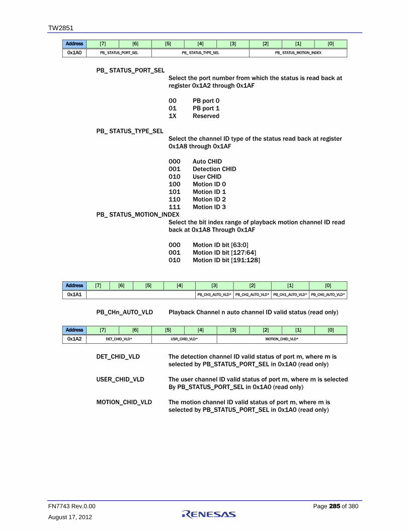
TW2851
FN7743 Rev.0.00 Page 285 of 380
August 17, 2012
Address [7] [6] [5] [4] [3] [2] [1] [0]
0x1A0 PB_ STATUS_PORT_SEL PB_ STATUS_TYPE_SEL PB_ STATUS_MOTION_INDEX
PB_ STATUS_PORT_SEL
Select the port number from which the status is read back at
register 0x1A2 through 0x1AF
00 PB port 0
01 PB port 1
1X Reserved
PB_ STATUS_TYPE_SEL
Select the channel ID type of the status read back at register
0x1A8 through 0x1AF
000 Auto CHID
001 Detection CHID
010 User CHID
100 Motion ID 0
101 Motion ID 1
110 Motion ID 2
111 Motion ID 3
PB_ STATUS_MOTION_INDEX
Select the bit index range of playback motion channel ID read
back at 0x1A8 Through 0x1AF
000 Motion ID bit [63:0]
001 Motion ID bit [127:64]
010 Motion ID bit [191:128]
Address [7] [6] [5] [4] [3] [2] [1] [0]
0x1A1 PB_CH3_AUTO_VLD* PB_CH2_AUTO_VLD* PB_CH1_AUTO_VLD* PB_CH0_AUTO_VLD*
PB_CHn_AUTO_VLD Playback Channel n auto channel ID valid status (read only)
Address [7] [6] [5] [4] [3] [2] [1] [0]
0x1A2 DET_CHID_VLD* USR_CHID_VLD* MOTION_CHID_VLD*
DET_CHID_VLD The detection channel ID valid status of port m, where m is
selected by PB_STATUS_PORT_SEL in 0x1A0 (read only)
USER_CHID_VLD The user channel ID valid status of port m, where m is selected
By PB_STATUS_PORT_SEL in 0x1A0 (read only)
MOTION_CHID_VLD The motion channel ID valid status of port m, where m is
selected by PB_STATUS_PORT_SEL in 0x1A0 (read only)
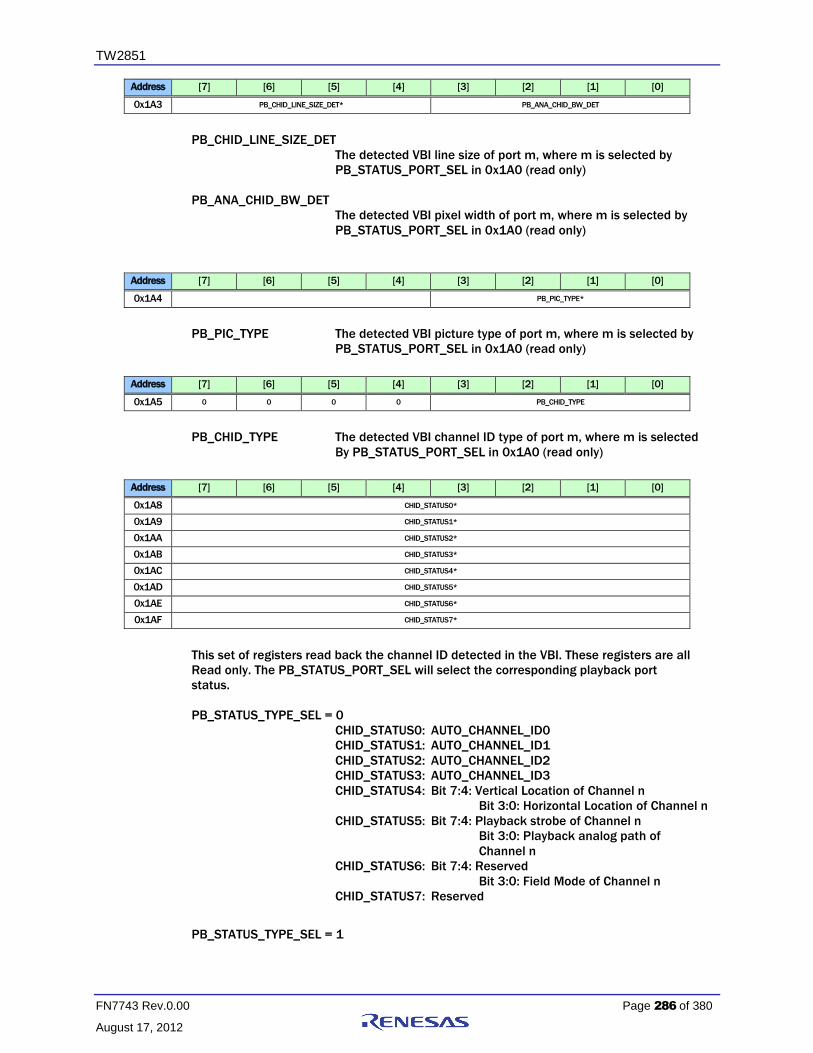
TW2851
FN7743 Rev.0.00 Page 286 of 380
August 17, 2012
Address [7] [6] [5] [4] [3] [2] [1] [0]
0x1A3 PB_CHID_LINE_SIZE_DET* PB_ANA_CHID_BW_DET
PB_CHID_LINE_SIZE_DET
The detected VBI line size of port m, where m is selected by
PB_STATUS_PORT_SEL in 0x1A0 (read only)
PB_ANA_CHID_BW_DET
The detected VBI pixel width of port m, where m is selected by
PB_STATUS_PORT_SEL in 0x1A0 (read only)
Address [7] [6] [5] [4] [3] [2] [1] [0]
0x1A4 PB_PIC_TYPE*
PB_PIC_TYPE The detected VBI picture type of port m, where m is selected by
PB_STATUS_PORT_SEL in 0x1A0 (read only)
Address [7] [6] [5] [4] [3] [2] [1] [0]
0x1A5 0 0 0 0 PB_CHID_TYPE
PB_CHID_TYPE The detected VBI channel ID type of port m, where m is selected
By PB_STATUS_PORT_SEL in 0x1A0 (read only)
Address [7] [6] [5] [4] [3] [2] [1] [0]
0x1A8 CHID_STATUS0*
0x1A9 CHID_STATUS1*
0x1AA CHID_STATUS2*
0x1AB CHID_STATUS3*
0x1AC CHID_STATUS4*
0x1AD CHID_STATUS5*
0x1AE CHID_STATUS6*
0x1AF CHID_STATUS7*
This set of registers read back the channel ID detected in the VBI. These registers are all
Read only. The PB_STATUS_PORT_SEL will select the corresponding playback port
status.
PB_STATUS_TYPE_SEL = 0
CHID_STATUS0: AUTO_CHANNEL_ID0
CHID_STATUS1: AUTO_CHANNEL_ID1
CHID_STATUS2: AUTO_CHANNEL_ID2
CHID_STATUS3: AUTO_CHANNEL_ID3
CHID_STATUS4: Bit 7:4: Vertical Location of Channel n
Bit 3:0: Horizontal Location of Channel n
CHID_STATUS5: Bit 7:4: Playback strobe of Channel n
Bit 3:0: Playback analog path of
Channel n
CHID_STATUS6: Bit 7:4: Reserved
Bit 3:0: Field Mode of Channel n
CHID_STATUS7: Reserved
PB_STATUS_TYPE_SEL = 1

TW2851
FN7743 Rev.0.00 Page 287 of 380
August 17, 2012
CHID_STATUS0: DET_CHANNEL_ID[7:0] of Chip ID 0
CHID_STATUS1: DET_CHANNEL_ID[15:8] of Chip ID 0
CHID_STATUS2: DET_CHANNEL_ID[7:0] of Chip ID 1
CHID_STATUS3: DET_CHANNEL_ID[15:8] of Chip ID 1
CHID_STATUS4: DET_CHANNEL_ID[7:0] of Chip ID 2
CHID_STATUS5: DET_CHANNEL_ID[15:8] of Chip ID 2
CHID_STATUS6: DET_CHANNEL_ID[7:0] of Chip ID 3
CHID_STATUS7: DET_CHANNEL_ID[15:8] of Chip ID 3
PB_STATUS_TYPE_SEL = 2
CHID_STATUS0: USER_CHANNEL_ID0[7:0]
CHID_STATUS1: USER_CHANNEL_ID0[15:8]
CHID_STATUS2: USER_CHANNEL_ID1[7:0]
CHID_STATUS3: USER_CHANNEL_ID1[15:8]
CHID_STATUS4: USER_CHANNEL_ID2[7:0]
CHID_STATUS5: USER_CHANNEL_ID2[15:8]
CHID_STATUS6: USER_CHANNEL_ID3[7:0]
CHID_STATUS7: USER_CHANNEL_ID3[15:8]
PB_STATUS_TYPE_SEL = 4 n is specified by PB_ STATUS_MOTION_INDEX
CHID_STATUS0: MOTION_CHANNEL_ID0[64*n+7:64*n]
CHID_STATUS1: MOTION_CHANNEL_ID0 [64*n+15 : 64 *n+8]
CHID_STATUS2: MOTION_CHANNEL_ID0[64*n+23 : 64 *n+16]
CHID_STATUS3: MOTION_CHANNEL_ID0[64*n+31:64 *n+24]
CHID_STATUS4: MOTION_CHANNEL_ID0[64*n+39:64 *n+32]
CHID_STATUS5: MOTION_CHANNEL_ID0[64*n+47:64 *n+40]
CHID_STATUS6: MOTION_CHANNEL_ID0[64*n+55:64 *n+48]
CHID_STATUS7: MOTION_CHANNEL_ID0[64*n+63:64 *n+56]
PB_STATUS_TYPE_SEL = 5 n is specified by PB_ STATUS_MOTION_INDEX
CHID_STATUS0: MOTION_CHANNEL_ID1[64*n+7:64*n],
CHID_STATUS1: MOTION_CHANNEL_ID1[64*n+15:64*
n+8]
CHID_STATUS2: MOTION_CHANNEL_ID1[64*n+23:64* n+16]
CHID_STATUS3: MOTION_CHANNEL_ID1[64*n+31:64* n+24]
CHID_STATUS4: MOTION_CHANNEL_ID1[64*n+39:64* n+32]
CHID_STATUS5: MOTION_CHANNEL_ID1[64*n+47:64* n+40]
CHID_STATUS6: MOTION_CHANNEL_ID1[64*n+55:64* n+48]
CHID_STATUS7: MOTION_CHANNEL_ID1[64*n+63:64* n+56]
PB_STATUS_TYPE_SEL = 6 n is specified by PB_ STATUS_MOTION_INDEX
CHID_STATUS0: MOTION_CHANNEL_ID2[64*n+7:64*n]
CHID_STATUS1: MOTION_CHANNEL_ID2[64*n+15:64* n+8]
CHID_STATUS2: MOTION_CHANNEL_ID2[64*n+23:64* n+16]
CHID_STATUS3: MOTION_CHANNEL_ID2[64*n+31:64* n+24]
CHID_STATUS4: MOTION_CHANNEL_ID2[64*n+39:64* n+32]
CHID_STATUS5: MOTION_CHANNEL_ID2[64*n+47:64* n+40]
CHID_STATUS6: MOTION_CHANNEL_ID2[64*n+55:64* n+48]
CHID_STATUS7: MOTION_CHANNEL_ID2[64*n+63:64* n+56]
PB_STATUS_TYPE_SEL = 7 n is specified by PB_ STATUS_MOTION_INDEX
CHID_STATUS0: MOTION_CHANNEL_ID3[64*n+7:64*n],
CHID_STATUS1: MOTION_CHANNEL_ID3[64*n+15:64* n+8]
CHID_STATUS2: MOTION_CHANNEL_ID3[64*n+23:64* n+16]
CHID_STATUS3: MOTION_CHANNEL_ID3[64*n+31:64* n+24]
CHID_STATUS4: MOTION_CHANNEL_ID3[64*n+39:64* n+32]
CHID_STATUS5: MOTION_CHANNEL_ID3[64*n+47:64 *n+40]
CHID_STATUS6: MOTION_CHANNEL_ID3[64*n+55:64* n+48]
CHID_STATUS7: MOTION_CHANNEL_ID3[64*n+63:64* n+56]

TW2851
FN7743 Rev.0.00 Page 288 of 380
August 17, 2012
Address [7] [6] [5] [4] [3] [2] [1] [0]
0x1C0 CVBS_SCL_HACTIVE[7:0]
0x1C1 CVBS_SCL_VACTIVE[7:0]
0x1C2 CVBS_SCL_VACTIVE[8] CVBS_SCL_HACTIVE[9:8]
CVBS_SCL_HACTIVE The horizontal active pixel number for display CVBS path
downscaler
CVBS_SCL_VACTIVE The vertical active line number for display CVBS path
downscaler
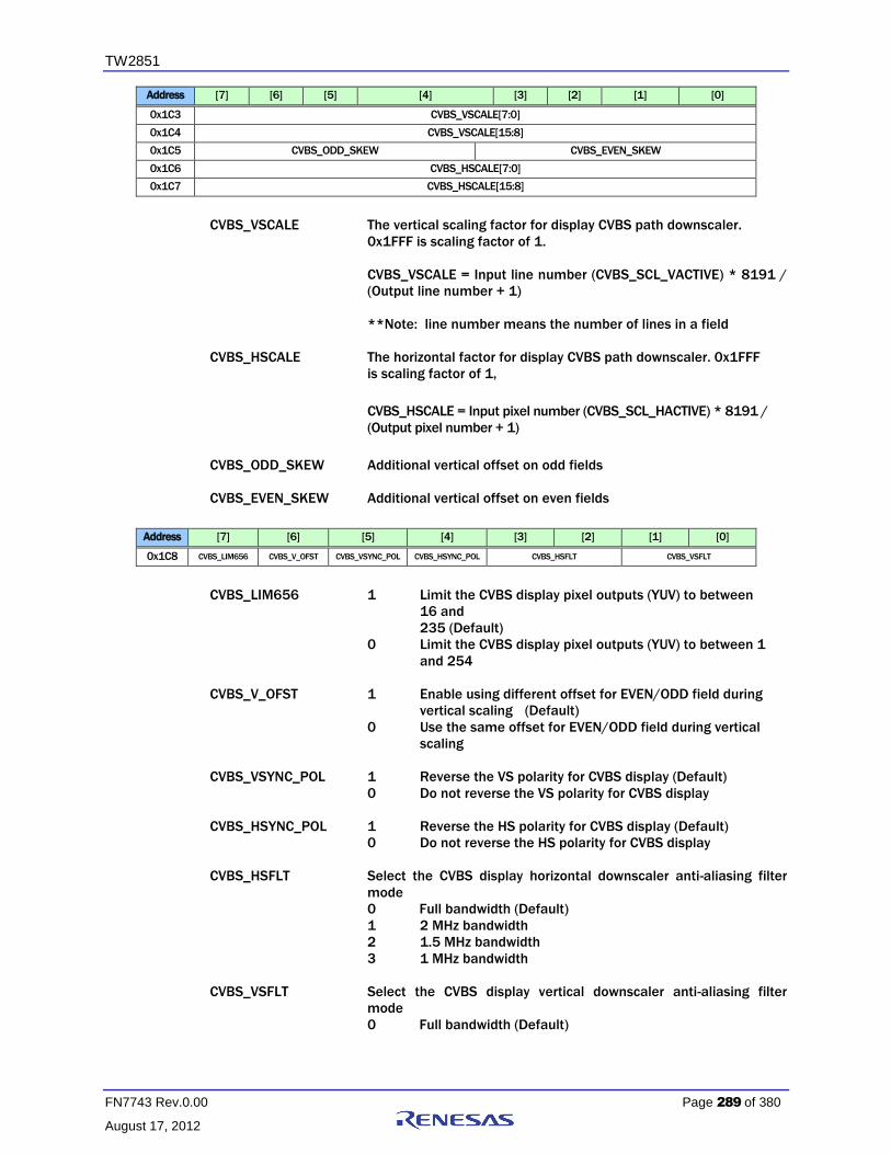
TW2851
FN7743 Rev.0.00 Page 289 of 380
August 17, 2012
Address [7] [6] [5] [4] [3] [2] [1] [0]
0x1C3 CVBS_VSCALE[7:0]
0x1C4 CVBS_VSCALE[15:8]
0x1C5 CVBS_ODD_SKEW CVBS_EVEN_SKEW
0x1C6 CVBS_HSCALE[7:0]
0x1C7 CVBS_HSCALE[15:8]
CVBS_VSCALE The vertical scaling factor for display CVBS path downscaler.
0x1FFF is scaling factor of 1.
CVBS_VSCALE = Input line number (CVBS_SCL_VACTIVE) * 8191 /
(Output line number + 1)
**Note: line number means the number of lines in a field
CVBS_HSCALE The horizontal factor for display CVBS path downscaler. 0x1FFF
is scaling factor of 1,
CVBS_HSCALE = Input pixel number (CVBS_SCL_HACTIVE) * 8191 /
(Output pixel number + 1)
CVBS_ODD_SKEW Additional vertical offset on odd fields
CVBS_EVEN_SKEW Additional vertical offset on even fields
Address [7] [6] [5] [4] [3] [2] [1] [0]
0x1C8 CVBS_LIM656 CVBS_V_OFST CVBS_VSYNC_POL CVBS_HSYNC_POL CVBS_HSFLT CVBS_VSFLT
CVBS_LIM656 1 Limit the CVBS display pixel outputs (YUV) to between
16 and
235 (Default)
0 Limit the CVBS display pixel outputs (YUV) to between 1
and 254
CVBS_V_OFST 1 Enable using different offset for EVEN/ODD field during
vertical scaling (Default)
0 Use the same offset for EVEN/ODD field during vertical
scaling
CVBS_VSYNC_POL 1 Reverse the VS polarity for CVBS display (Default)
0 Do not reverse the VS polarity for CVBS display
CVBS_HSYNC_POL 1 Reverse the HS polarity for CVBS display (Default)
0 Do not reverse the HS polarity for CVBS display
CVBS_HSFLT Select the CVBS display horizontal downscaler anti-aliasing filter
mode
0 Full bandwidth (Default)
1 2 MHz bandwidth
2 1.5 MHz bandwidth
3 1 MHz bandwidth
CVBS_VSFLT Select the CVBS display vertical downscaler anti-aliasing filter
mode
0 Full bandwidth (Default)

TW2851
FN7743 Rev.0.00 Page 290 of 380
August 17, 2012
1 0.25 line-rate bandwidth
2,3 0.18 line-rate bandwidth
Address [7] [6] [5] [4] [3] [2] [1] [0]
0x1C9 0 0 0 0 CVBS_FLD_POL CVBS_T_FDLY CVBS_T_VSCL CVBS_T_CPALDLY
CVBS_FLD_POL 1 Reverse the Display CVBS field polarity
0 Do not reverse the field polarity
CVBS_T_FDLY Set display CVBS scaler field delay mode for testing
CVBS_T_VSCL Set display CVBS vertical scaler scaling factor to be 1 for testing
CVBS_T_CPALDLY Set display CVBS scaler chroma delay in PAL mode
Address [7] [6] [5] [4] [3] [2] [1] [0]
0x1CA CVBS_TEST CVBS_SOFT_RST CVBS_HSCL_BP CVBS_PALDLY
CVBS_TEST 0001 Enable display CVBS scaler test pattern with data valid
from the pattern generator
0010 Enable display CVBS scaler test pattern with data valid
from the display path
CVBS_SOFT_RST Display CVBS scaler software reset
CVBS_HSCL_BP Bypass display CVBS horizontal scaler
CVBS_PALDLY Set PAL delay mode
Address [7] [6] [5] [4] [3] [2] [1] [0]
0x1CB C_V_START
0x1CC C_V_END [7:0]
0x1CD C_LINE_INS C_V_END[8]
C_V_START Set the starting line number of active video shown in PAL mode
C_V_END Set the end line number of active video shown in PAL mode
C_LINE_INS Enable inserting blanking lines at the beginning and end in PAL
mode

TW2851
FN7743 Rev.0.00 Page 291 of 380
August 17, 2012
Address [7] [6] [5] [4] [3] [2] [1] [0]
0x1D0 INTERRUPT_VECT0
0x1D1 INTERRUPT_VECT1
0x1D2 INTERRUPT_VECT2
0x1D3 INTERRUPT_VECT3
0x1D4 INTERRUPT_VECT4
0x1D5 INTERRUPT_VECT5
0x1D6 INTERRUPT_VECT6
0x1D7 INTERRUPT_VECT7
0x1D8 INTERRUPT_VECT_MASK0
0x1D9 INTERRUPT_VECT_MASK1
0x1DA INTERRUPT_VECT_MASK2
0x1DB INTERRUPT_VECT_MASK3
0x1DC INTERRUPT_VECT_MASK4
0x1DD INTERRUPT_VECT_MASK5
0x1DE INTERRUPT_VECT_MASK6
0x1DF INTERRUPT_VECT_MASK7
0x1E0 INTERRUPT_STATUS
INTERRUPT_VECTn Read Read the interrupt status of the specific interrupt source
Write Write a ‘1’ to that bit will clear the specific interrupt
source. This clear bit will make the INTERRUPT_VECT
to become ‘0’
INTERRUPT_VECT_MASKn
1 Set to ‘1’ will allow the INTERRUPT_VECT source to
show up at the output IRQ pin if the vector bit is a ‘1’
0 Set to ‘0’ will disable the output to IRQ, so the MCU will
ignore that source
INTERRUPT_STATUS[x]
1 An INTERRUPT_STATUS[x] of ‘1’ means there is some
source in INTERRUPT_VECTx set to 1. The MCU can read
this register before it read each of the INTERRUPT_VECTx.
The specific interrupt vector is organized as follows:
INTERRUPT_VECT0[3:0] Video Decoder Motion
Detection, ANA_SW = 0
INTERRUPT_VECT0[7:4] Video Decoder Motion
Detection, ANA_SW = 1
INTERRUPT_VECT1[3:0] Video Decoder Night Detection,
ANA_SW = 0
INTERRUPT_VECT1[7:4] Video Decoder Night Detection,
ANA_SW = 1
INTERRUPT_VECT2[3:0] Video Decoder Black Detection,
ANA_SW = 0
INTERRUPT_VECT2[7:4] Video Decoder Black Detection,
ANA_SW = 1
INTERRUPT_VECT3[3:0] Video Decoder NO VIDEO
detection, ANA_SW = 0
INTERRUPT_VECT3[7:4] Video Decoder NO VIDEO
detection, ANA_SW = 1
INTERRUPT_VECT4[3:0] Unused
INTERRUPT_VECT4[7:4] Playback port CHID Detection
INTERRUPT_VECT5[3:0] Playback port NO VIDEO

TW2851
FN7743 Rev.0.00 Page 292 of 380
August 17, 2012
Detection
INTERRUPT_VECT5[7:4] Playback muxed channel PORT
Change Detection
INTERRUPT_VECT6[0] Display Strobe Done
INTERRUPT_VECT6[1] Record Strobe Done
INTERRUPT_VECT6[2] SPOT Strobe Done
INTERRUPT_VECT6[3] Record Read/Write Switch
Queue Done
INTERRUPT_VECT6[4] SPOT Read/Write Switch
Queue Done
INTERRUPT_VECT6[5] PS2 Mouse Interrupt
INTERRUPT_VECT6[6] OSG Bitmap Done (or Wait)
INTERRUPT_VECT6[7] DDC Channel Interrupt
INTERRUPT_VECT7[0] Display VGA Vstart
INTERRUPT_VECT7[1] Display CVBS Vstart
INTERRUPT_VECT7[2] Record Vstart
INTERRUPT_VECT7[3] SPOT Vstart
INTERRUPT_VECT7[4] Unused
INTERRUPT_VECT7[5] Unused
INTERRUPT_VECT7[6] Unused
INTERRUPT_VECT7[7] Unused
Page 2: 0x200 ~ 0x2FE
Address [7] [6] [5] [4] [3] [2] [1] [0]
0x200 0 0 RP_INP_FLD_POL RP_CC_EN 0 RP_CLK_SEL
RP_INP_FLD_POL Reverse the field polarity for record path only
RP_CC_EN[1] 1 Record Cascade Output Enable
0 Record Cascade Output Disable
This feature is not available in TW2851 rev B2. This bit is always
set to 0.
RP_CC_EN[0] 1 Record Cascade Input Enable
0 Record Cascade Input Disable
This feature is not available in TW2851 rev B2. This bit is always
set to 0.
RP_CLK_SEL Record Path Clock Selection
0 Reserved
1 27 MHz for 1 port 656, 13.5 MHz for 2 port 656 or 601
2 54 MHz for 1 port 656, 27 MHz for 2 port 656 or 601
3 108 MHz for 1 port 656, 54 MHz for 2 port 656, 601, or
1120
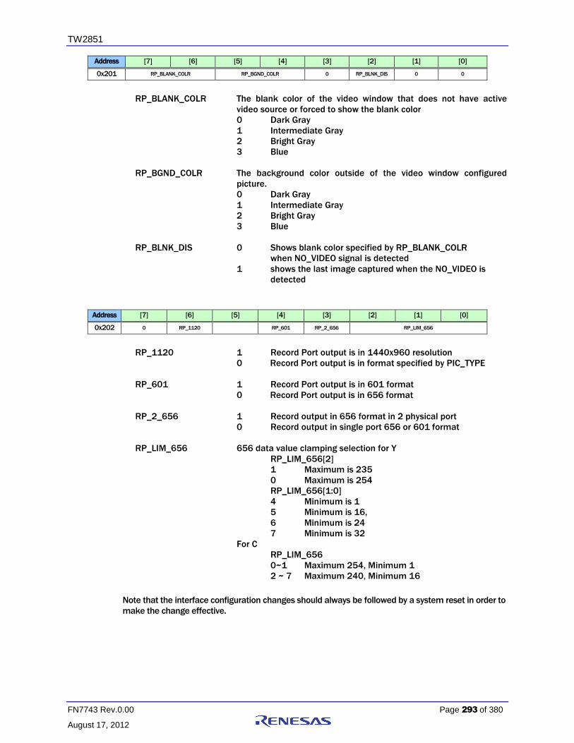
TW2851
FN7743 Rev.0.00 Page 293 of 380
August 17, 2012
Address [7] [6] [5] [4] [3] [2] [1] [0]
0x201 RP_BLANK_COLR RP_BGND_COLR 0 RP_BLNK_DIS 0 0
RP_BLANK_COLR The blank color of the video window that does not have active
video source or forced to show the blank color
0 Dark Gray
1 Intermediate Gray
2 Bright Gray
3 Blue
RP_BGND_COLR The background color outside of the video window configured
picture.
0 Dark Gray
1 Intermediate Gray
2 Bright Gray
3 Blue
RP_BLNK_DIS 0 Shows blank color specified by RP_BLANK_COLR
when NO_VIDEO signal is detected
1 shows the last image captured when the NO_VIDEO is
detected
Address [7] [6] [5] [4] [3] [2] [1] [0]
0x202 0 RP_1120 RP_601 RP_2_656 RP_LIM_656
RP_1120 1 Record Port output is in 1440x960 resolution
0 Record Port output is in format specified by PIC_TYPE
RP_601 1 Record Port output is in 601 format
0 Record Port output is in 656 format
RP_2_656 1 Record output in 656 format in 2 physical port
0 Record output in single port 656 or 601 format
RP_LIM_656 656 data value clamping selection for Y
RP_LIM_656[2]
1 Maximum is 235
0 Maximum is 254
RP_LIM_656[1:0]
4 Minimum is 1
5 Minimum is 16,
6 Minimum is 24
7 Minimum is 32
For C
RP_LIM_656
0~1 Maximum 254, Minimum 1
2 ~ 7 Maximum 240, Minimum 16
Note that the interface configuration changes should always be followed by a system reset in order to
make the change effective.

TW2851
FN7743 Rev.0.00 Page 294 of 380
August 17, 2012
Address [7] [6] [5] [4] [3] [2] [1] [0]
0x203 RP_H_OFFSET
0x204 0 RP_V_OFFSET
0x205 RP_H_SIZE[7:0]
0x206 RP_V_SIZE[7:0]
0x207 0 0 0 0 0 RP_V_SIZE[8] RP_H_SIZE[9:8]
RP_H_OFFSET The horizontal offset of the first active pixel in the output 656/601
format
RP_V_OFFSET The vertical offset of the first active line in the output 656/601
format
RP_H_SIZE The horizontal active length used to show the video pictures
RP_V_SIZE The vertical active height used to show the video pictures
Address [7] [6] [5] [4] [3] [2] [1] [0]
0x208 RP_SQ_CMD RP_SQ_WR RP_SQ_RW_DONE* 0 0 0 0 RP_CONFIG_DONE
RP_SQ_CMD The command bit to start a Record Path Switch Queue read / write
operation. Set to 1 to start a command. This bit wills self clear.
RP_SQ_WR Read/Write Flag for Record Path Switch Queue operation
1 Write to Switch Queue
0 Read from Switch Queue
RP_SQ_RW_DONE Read Only
RP_CONFIG_DONE After any configuration changes are made to the record path
control registers, this bit should be set to resume the record path
operation.

TW2851
FN7743 Rev.0.00 Page 295 of 380
August 17, 2012
Address [7] [6] [5] [4] [3] [2] [1] [0]
0x209 RP_SQ_ DATA[7:0]
0x20A RP_SQ_ DATA[15:8]
0x20B RP_SQ_ DATA[23:16]
0x20C RP_SQ_ DATA[31:24]
RP_SQ_DATA0 ~ 3 are used to read/write the data from/to the record path switch queue
entry when a switch queue read/write operation is performed.
In write operation, these 4 registers are written first. Then a command is issued using
RP_SQ_CMD in 0x208 to move the data into the switching queue.
In read operation, a read command is issued using RP_SQ_CMD in 0x208 to move the
data from switch queue into these 4 registers. The MCU can then read the entry from
these registers.
The definition of each bit used in the switch queue entry is as follows.
RP_SQ_DATA[1:0] Port ID for channel 0 (upper left window)
RP_SQ_DATA[3:2] Chip ID for channel 0
RP_SQ_DATA[5:4] Port ID for Channel 1 (upper right window)
RP_SQ_DATA[7:6] Chip ID for Channel 1
RP_SQ_DATA[9:8] Port ID for Channel 2 (Lower left window)
RP_SQ_DATA[11:10] Chip ID for Channel 2
RP_SQ_DATA[13:12] Port ID for Channel 3 (Lower right window)
RP_SQ_DATA[15:14] Chip ID for Channel 3
RP_SQ_DATA[19:16] Channel 0 ~ 3 disable bit.
Bit 16 set to 1, Channel 0 is disabled.
Bit 17 set to 1, Channel 1 is disabled
Bit 18 set to 1, Channel 2 is disabled
Bit 19 set to 1, Channel 3 is disabled
RP_SQ_DATA[22:20] Picture Type, as shown in Figure 15
RP_SQ_DATA[23] Strobe field type for field mode picture type.
1 Odd field
0 Even field
RP_SQ_DATA[25:24] Field/Frame based OSD0 selection for Record Output Port 0. There
will be 4 sets of OSD0 configuration information. These 2 bits
selects one of the 4 sets for record output port 0. According to
the setting of these 2 bits, the OSD result can change from field to
field or frame to frame.
RP_SQ_DATA[27:26] Field/Frame based OSD1 selection for Record Output Port 1. There
will be 4 sets of OSD1 configuration information. These 2 bits
selects one of the 4 sets for record output port 1. According to the
setting of these 2 bits, the OSD result can change from field to field
or frame to frame.
RP_SQ_DATA[31:28] Reserved

TW2851
FN7743 Rev.0.00 Page 296 of 380
August 17, 2012
Address [7] [6] [5] [4] [3] [2] [1] [0]
0x20D RP_SQ_ ADDR[7:0]
0x20E RP_SQ_ SIZE[7:0]
0x20F 0 RP_SQ_SIZE[10:8] 0 RP_SQ_ADDR[10:8]
RP_SQ_ADDR The switch queue entry address to perform the switch queue
read / write command. This address is automatically incremented
after the command is performed
RP_SQ_SIZE The switch queue size.
1-2047: 1-2047
2048: 0
Address [7] [6] [5] [4] [3] [2] [1] [0]
0x210 RP_CH_EN_0 0 RP_FUNC_MD_0 RP_ANA_0 0 RP_BLNK_0 RP_MIR_V_0 RP_MIR_H_0
0x211 RP_CH_EN_1 0 RP_FUNC_MD_1 RP_ANA_1 0 RP_BLNK_1 RP_MIR_V_1 RP_MIR_H_1
0x212 RP_CH_EN_2 0 RP_FUNC_MD_2 RP_ANA_2 0 RP_BLNK_2 RP_MIR_V_2 RP_MIR_H_2
0x213 RP_CH_EN_3 0 RP_FUNC_MD_3 RP_ANA_3 0 RP_BLNK_3 RP_MIR_V_3 RP_MIR_H_3
RP_CH_EN Channel Enable Control for each of channel 0 through 3
1 Enable channel
0 Disable channel
RP_FUNC_MD When the Record Path is not in Switch mode, this bit specifies the
record capture mode
1 Strobe Mode
0 Live Mode
RP_ANA Specify the analog input selection of each of the channel.
0 VINA
1 VINB
RP_BLNK Force the channel to display blank color
1 Blank
0 Normal video
RP_MIR_V Control to mirror the image vertically for each channel
0 Do not mirror vertically
1 Mirror vertically
RP_MIR_H Control to mirror the image horizontally for each channel
0 Do not mirror horizontally
1 Mirror horizontally
Address [7] [6] [5] [4] [3] [2] [1] [0]
0x214 0 0 0 0 RP_STROBE_3 RP_STROBE_2 RP_STROBE_1 RP_STROBE_0
RP_STROBE Strobe command for each channel. Once set to 1, the
corresponding channel will capture one field/frame and then clear
this bit.

TW2851
FN7743 Rev.0.00 Page 297 of 380
August 17, 2012
Address [7] [6] [5] [4] [3] [2] [1] [0]
0x215 0 RP_STRB_FLD RP_CH_CYCLE RP_SM_EN RP_PIC_TYPE
RP_STRB_FLD In non-switch mode, this bit controls which field to capture in field
mode ( pic_type 0, 2, 4, 6, 7)
0 Capture Even field
1 Capture Odd field
RP_CH_CYCLE In non-switch mode, this RP_CH_CYCLE controls how many
channels to interleave when the pic_type is 0, 1, 6, and 7.
PIC_TYPE 0, 1
0 Capture and interleave channel 0, 1, 2, 3
1 Capture channel 0
2 Capture and interleave channel 0, 1
3 Capture and interleave channel 0, 1, 2
PIC_TYPE 6, 7
1 Capture channel 0, 1
2 Capture and interleave channel 0, 1, 2, 3
RP_SM_EN 1 Record Path is in Switch Queue Mode
0 Record Path is in Live or Strobe Mode
RP_PIC_TYPE When Record Path is not in Switch Queue Mode, RP_PIC_TYPE
specifies the pic_type used in LIVE/Strobe mode
Address [7] [6] [5] [4] [3] [2] [1] [0]
0x216 RP_MOTN_ID_EN RP_DIG_ID_EN RP_ANA_ID_EN RP_ANA_RIC_EN RP_AUTO_ID_EN RP_AUTO_RPT_EN RP_DET_ID_EN RP_USR_ID_EN
RP_MOTN_ID_EN 1 Turn on motion information encoding
0 Do not turn on motion information encoding
RP_DIG_ID_EN 1 Turn on the digital channel ID encoding
0 Turn off the digital channel ID encoding
RP_ANA_ID_EN 1 Turn on the analog channel ID encoding
0 Turn off the analog channel ID encoding
RP_ANA_RPT_EN 1 Turn on the analog auto channel ID repeat line
0 Turn off the analog auto channel ID repeat line
RP_AUTO_ID_EN 1 Turn on the auto channel ID encoding
0 Turn off the auto channel ID encoding
RP_DET_ID_EN 1 Turn on the detection ID encoding
0 Turn off the detection ID encoding
RP_USR_ID_EN 1 Turn on the user information encoding
0 Turn off the user information encoding

TW2851
FN7743 Rev.0.00 Page 298 of 380
August 17, 2012
Address [7] [6] [5] [4] [3] [2] [1] [0]
0x217 RP_ANA_CHID_H_OFST
RP_ANA_CHID_H_OFST
The horizontal starting offset for Analog Channel ID
Address [7] [6] [5] [4] [3] [2] [1] [0]
0x218 RP_ANA_CHID_HIGH
0x219 RP_ANA_CHID_LOW
RP_ANA_CHID_HIGH Pixel values bigger than this setting are interpreted as “1” for
Analog Channel ID (default: 235)
RP_ANA_CHID_LOW Pixel values smaller than this setting are interpreted as “0” for
Analog Channel ID (default: 16)
Address [7] [6] [5] [4] [3] [2] [1] [0]
0x21A RP_CHID_V_OFSTO 0 RP_CHID_V_OFST
0x21B RP_CHID_V_OFSTE RP_USR_ID_PT_SEL RP_ANA_CHID_BW
RP_CHID_V_OFSTO Control the vertical starting offset on top of RP_CHID_V_OFST in
odd field for Analog Channel ID
RP_CHID_V_OFSTE Control the vertical starting offset on top of RP_CHID_V_OFST in
even field for Analog Channel ID
RP_CHID_V_OFST Vertical starting offset for Analog Channel ID. The actual vertical
line offset is RP_CHID_V_OFST + RP_CHID_V_OFSTO or
RP_CHID_V_OFST + RP_CHID_V_OFSTE
RP_ANA_CHID_BW Control the pixel width of each bit for Analog Channel ID
0 1 pixel
: :
31 32 pixels (default)
RP_USER_ID_PT_SEL This bit is used to select the user channel ID registers in 0x220 ~
0x227 information is to be used for either record port 0 or 1
0 0x220 ~ 0x227 are used for record port 0
1 0x220 ~ 0x227 are used for record port 1
Address [7] [6] [5] [4] [3] [2] [1] [0]
0x21C RP_SMALL_FR RP_BI_CLK RP_BYPASS RP_GEN_CTL
RP_GEN_CTL Internal test function
RP_BYPASS Enable bypass from video decoder to record output pin with byte-
interleaving format
0 Disable bypass
1 Enable bypass
RP_BI_CLK Use 27 MHz CLKOY and CLKOYB for Byte Interleaving Output. This
bit is valid only when RP_BYPASS is set to 1.
0 27 MHz

TW2851
FN7743 Rev.0.00 Page 299 of 380
August 17, 2012
1 54 MHz
RP_SMALL_FR Internal test function
Address [7] [6] [5] [4] [3] [2] [1] [0]
0x21D RP_CHNUM1 RP_CHNUM0
0x21E RP_CHNUM3 RP_CHNUM2
0x21F RP_GEN_FLDPOL
RP_CHNUM The Channel Number to display in non-switch mode
[3:2] CHIP ID
[1:0] PORT ID
RP_GEN_FLDPOL Reverse the field polarity of the internal pattern generator for RP
path.
Address [7] [6] [5] [4] [3] [2] [1] [0]
0x220 RP_USER_CHID[7:0]
0x221 RP_USER_CHID[15:8]
0x222 RP_USER_CHID[23:16]
0x223 RP_USER_CHID[31:24]
0x224 RP_USER_CHID[39:32]
0x225 RP_USER_CHID[47:40]
0x226 RP_USER_CHID[55:48]
0x227 RP_USER_CHID[63:56]
RP_USER_CHID Used to set the USER Channel ID for record path.
Depending on the RP_USER_ID_PT_SEL (0x21B bit 5), these can
be used to read/write the user channel ID for record port 0,
or record port 1. Always set RP_USER_ID_PT_SEL before any
read/write to these registers
Address [7] [6] [5] [4] [3] [2] [1] [0]
0x228 RP_HALF_LINE[7:0]
0x229 RP_HALF_LINE[9:8] RP_HS_P_OS
0x22A RP_HS_WIDTH
RP_HALF_LINE This defines in number of clock cycles from VS edge to the location
of field change, in case it is change in middle of a line
RP_HS_P_OS HSYNC starting location, in number of clock cycles
RP_HS_WIDTH HSYNC width, in number of clock cycles

TW2851
FN7743 Rev.0.00 Page 300 of 380
August 17, 2012
Address [7] [6] [5] [4] [3] [2] [1] [0]
0x22B RP_TOP_VS_END
0x22C RP_BOT_VS_END
0x22D RP_T_VS_POS RP_TOP_VS_OS
0x22E RP_B_VS_PS RP_BOT_VS_OS
RP_TOP_VS_END VSYNC trailing edge location of top field, in number of lines
RP_BOT_VS_END VSYNC trailing edge location of bottom field, in number of lines
RP_TOP_VS_OS VSYNC leading edge location of top field, in number of lines
RP_BOT_VS_OS VSYNC leading edge location of bottom field, in number of lines
RP_T_VS_POS Enable the top field vsync edge at the middle of a line
RP_B_VS_POS Enable the bottom field vsync edge at the middle of a line
Address [7] [6] [5] [4] [3] [2] [1] [0]
0x22F RP_HS_POL RP_VS_POL RP_FLD_POL RP_VAV_POL RP_HAV_POL RP_ 656_ERRCHK
RP_HS_POL Output HSYNC polarity control
RP_VS_POL Output VSYNC polarity control
RP_FLD_POL Output FIELD polarity control
RP_VAV_POL Output VAV polarity control
RP_HAV_POL Output HAV polarity control
RP_656_ERRCHK Enable 656 SAV/EAV error check

TW2851
FN7743 Rev.0.00 Page 301 of 380
August 17, 2012
Address [7] [6] [5] [4] [3] [2] [1] [0]
0x230 DP_BLANK_COLR DP_BGND_COLR
DP_BLANK_COLR[3]
1 Blue
0 Gray, the gray level is selected by
DP_BLANK_COLR[2:0]
DP_BLANK_COLR[2:0]
0 ~ 3 Black
4 Gray darkest
5 Gray darker
6 Gray lighter
7 Gray lightest
DP_BGND_COLR[3]
1 Blue
0 Gray, the gray level is selected by
DP_BGND_COLR[2:0]
DP_BGND_COLR[2:0]
0 ~ 3 Black
4 Gray darkest
5 Gray darker
6 Gray lighter
7 Gray lightest
Address [7] [6] [5] [4] [3] [2] [1] [0]
0x231 DP_LIM_656 DP_CVBS_VSPOL DP_FIELD_ID DP_WINWIDTH
DP_LIM_656 656 Data Clamping
For Y:
DP_LIM_656[2]
0 Maximum limit to 254
1 Maximum limit to 235
DP_LIM_656[1:0]
0 Minimum set to 1
1 Minimum set to 16
2 Minimum set to 24
3 Minimum set to 32
For C
DP_LIM_656
0 Maximum 254, Minimum 1
1~7 Maximum 240, Minimum 16
DP_CVBS_VSPOL 0 Do not reverse the VS polarity for CVBS
1 Reverse the VS polarity for CVBS
DP_FIELD_ID 1 Force the output to de-interlacer to top field
0 Do not force field ID to top field
DP_WINWIDTH 1 1440 pixels maximum per line
0 720 pixels maximum per line

TW2851
FN7743 Rev.0.00 Page 302 of 380
August 17, 2012
Address [7] [6] [5] [4] [3] [2] [1] [0]
0x232 DP_SOFTRST DP_DI_FLDPOL 0 0 0 0 0 0
DP_SOFTRST 1 Reset Display Path
0 Do not reset the display path
DP_DI_FLDPOL 1 Reverse the field polarity to the VGA de-interlacer
0 Do not reverse the field polarity to the de-interlacer
Address [7] [6] [5] [4] [3] [2] [1] [0]
0x237 DP_CAS_IN_EN
DP_CAS_IN_EN Enable the display cascade input
Address [7] [6] [5] [4] [3] [2] [1] [0]
0x238 1 0
Reserved
Address [7] [6] [5] [4] [3] [2] [1] [0]
0x23A DP_BORDER_BLINK
DP_BORDER_BLINK 1 Turn on border blinking for the corresponding window 0
~ 7
0 Turn off border blinking
Address [7] [6] [5] [4] [3] [2] [1] [0]
0x23B DP_VGA_FLDPOL DP_CVBS_FLDPOL DP_VD_FLDPOL
DP_VGA_FLDPOL Reverse the field polarity for the display VGA output
DP_CVBS_FLDPOL Reverse the field polarity for the display CVBS output
DP_VD_FLDPOL Reverse the field polarity of the incoming video stream
Address [7] [6] [5] [4] [3] [2] [1] [0]
0x23C DP_FREEZEOPT[7:0]
0x23D DP_ADAPT_EN[7:0]
DP_FREEZEOPT 0 Display field only when freeze command is issued or
underflow condition occurs
1 Display frame when freeze command is issued or
underflow condition occurs
DP_ADAPT_EN 0 Display field/frame according to DP_FREEZEOPT
1 Overwrite DP_FREEZEOPT and display frame when
no_motion is asserted
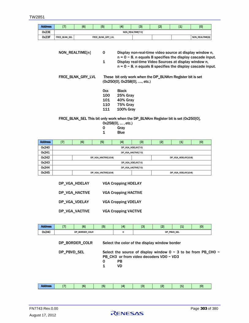
TW2851
FN7743 Rev.0.00 Page 303 of 380
August 17, 2012
Address [7] [6] [5] [4] [3] [2] [1] [0]
0x23E NON_REALTIME[7:0]
0x23F FRCE_BLNK_SEL FRCE_BLNK_GRY_LVL NON_REALTIME[8]
NON_REALTIME[n] 0 Display non-real-time video source at display window n,
n = 0 ~ 8. n equals 8 specifies the display cascade input.
1 Display real-time Video Sources at display window n,
n = 0 ~ 8. n equals 8 specifies the display cascade input.
FRCE_BLNK_GRY_LVL These bit only work when the DP_BLNKm Register bit is set
(0x250[0], 0x258[0], …., etc.)
0xx Black
100 25% Gray
101 40% Gray
110 75% Gray
111 100% Gray
FRCE_BLNK_SEL This bit only work when the DP_BLNKm Register bit is set (0x250[0],
0x258[0], … , etc.)
0 Gray
1 Blue
Address [7] [6] [5] [4] [3] [2] [1] [0]
0x240 DP_VGA_HDELAY[7:0]
0x241 DP_VGA_HACTIVE[7:0]
0x242 DP_VGA_HACTIVE[10:8] DP_VGA_HDELAY[10:8]
0x243 DP_VGA_VDELAY[7:0]
0x244 DP_VGA_VACTIVE[7:0]
0x245 DP_VGA_VACTIVE[10:8] DP_VGA_VDELAY[10:8]
DP_VGA_HDELAY VGA Cropping HDELAY
DP_VGA_HACTIVE VGA Cropping HACTIVE
DP_VGA_VDELAY VGA Cropping VDELAY
DP_VGA_VACTIVE VGA Cropping VACTIVE
Address [7] [6] [5] [4] [3] [2] [1] [0]
0x24C DP_BORDER_COLR 0 DP_PBVD_SEL
DP_BORDER_COLR Select the color of the display window border
DP_PBVD_SEL Select the source of display window 0 ~ 3 to be from PB_CH0 ~
PB_CH3 or from video decoders VD0 ~ VD3
0 PB
1 VD
Address [7] [6] [5] [4] [3] [2] [1] [0]

TW2851
FN7743 Rev.0.00 Page 304 of 380
August 17, 2012
0x24D DP_CHNAB_SEL
DP_CHNAB_SEL Select the Analog Switch A/B for each window 0 ~ 7
Address [7] [6] [5] [4] [3] [2] [1] [0]
0x24E DP_BORDER_EN
DP_BORDER_EN Enable display window borders for each window 0 ~ 7
Address [7] [6] [5] [4] [3] [2] [1] [0]
0x24F DP_STRB_REQ
DP_STRB_REQ Strobe Request to each of the 8 windows. Self clear after the
strobe is done
Address [7] [6] [5] [4] [3] [2] [1] [0]
0x250 DP_CH_EN0 DP_FREEZE0 DP_STRB_FLD0 DP_FUNC_MD0 DP_RD_V_2X0 DP_BLNK0
0x258 DP_CH_EN1 DP_FREEZE1 DP_STRB_FLD1 DP_FUNC_MD1 DP_RD_V_2X1 DP_BLNK1
0x260 DP_CH_EN2 DP_FREEZE2 DP_STRB_FLD2 DP_FUNC_MD2 DP_RD_V_2X2 DP_BLNK2
0x268 DP_CH_EN3 DP_FREEZE3 DP_STRB_FLD3 DP_FUNC_MD3 DP_RD_V_2X3 DP_BLNK3
0x270 DP_CH_EN4 DP_FREEZE4 DP_STRB_FLD4 DP_FUNC_MD4 DP_RD_V_2X4 DP_BLNK4
0x278 DP_CH_EN5 DP_FREEZE5 DP_STRB_FLD5 DP_FUNC_MD5 DP_RD_V_2X5 DP_BLNK5
0x280 DP_CH_EN6 DP_FREEZE6 DP_STRB_FLD6 DP_FUNC_MD6 DP_RD_V_2X6 DP_BLNK6
0x288 DP_CH_EN7 DP_FREEZE7 DP_STRB_FLD7 DP_FUNC_MD7 DP_RD_V_2X7 DP_BLNK7
DP_CH_ENm 1 Enable window m
0 Disable window m
DP_FREEZEm 1 Freeze window m
0 Do not freeze window m
DP_STRB_FLDm 0 Strobe at Odd Field
1 Strobe at Even Field
2/3 Strobe at Frame
DP_FUNC_MDm 0 LIVE Mode
1 Strobe Mode
2/3 Reserved
DP_RD_V_2Xm 1 Scale Up 2X vertically (For CIF becoming D1)
0 Do not scale up 2X
DP_BLNKm 1 Force the window m to display blank color
0 Show normal video in the window m

TW2851
FN7743 Rev.0.00 Page 305 of 380
August 17, 2012
Address [7] [6] [5] [4] [3] [2] [1] [0]
0x251 DP_OVWR_V2X0 DP_MIR_H_0 DP_MIR_V_0
0x259 DP_OVWR_V2X1 DP_MIR_H_1 DP_MIR_V_1
0x261 DP_OVWR_V2X2 DP_MIR_H_2 DP_MIR_V_2
0x269 DP_OVWR_V2X3 DP_MIR_H_3 DP_MIR_V_3
0x271 DP_OVWR_V2X4 DP_MIR_H_4 DP_MIR_V_4
0x279 DP_OVWR_V2X5 DP_MIR_H_5 DP_MIR_V_5
0x281 DP_OVWR_V2X6 DP_MIR_H_6 DP_MIR_V_6
0x289 DP_OVWR_V2X7 DP_MIR_H_7 DP_MIR_V_7
DP_OVWR_V2X Force V2X write, instead of following pic_type. I.e., write even
line to top field, and odd line to bottom field.
DP_MIR_H_n 1 Mirror horizontally
0 Do not mirror horizontally
DP_MIR_V_n 1 Mirror vertically
0 Do not mirror vertically
Address [7] [6] [5] [4] [3] [2] [1] [0]
0x252 DP_PICHL0[7:0]
0x253 DP_PICHR0[7:0]
0x254 DP_PICVT0
0x255 DP_PICVB0
0x256 0 DP_PICHR0[8] DP_PICHL0[8]
0x25A DP_PICHL1[7:0]
0x25B DP_PICHR1[7:0]
0x25C DP_PICVT1
0x25D DP_PICVB1
0x25E 1 DP_PICHR1[8] DP_PICHL1[8]
0x262 DP_PICHL2[7:0]
0x263 DP_PICHR2[7:0]
0x264 DP_PICVT2
0x265 DP_PICVB2
0x266 2 DP_PICHR2[8] DP_PICHL2[8]
0x26A DP_PICHL3[7:0]
0x26B DP_PICHR3[7:0]
0x26C DP_PICVT3
0x26D DP_PICVB3
0x26E 3 DP_PICHR3[8] DP_PICHL3[8]
0x272 DP_PICHL4[7:0]
0x273 DP_PICHR4[7:0]
0x274 DP_PICVT4
0x275 DP_PICVB4
0x276 4 DP_PICHR4[8] DP_PICHL4[8]
0x27A DP_PICHL5[7:0]
0x27B DP_PICHR5[7:0]
0x27C DP_PICVT5
0x27D DP_PICVB5
0x27E 5 DP_PICHR5[8] DP_PICHL5[8]
0x282 DP_PICHL6[7:0]
0x283 DP_PICHR6[7:0]
0x284 DP_PICVT6

TW2851
FN7743 Rev.0.00 Page 306 of 380
August 17, 2012
Address [7] [6] [5] [4] [3] [2] [1] [0]
0x285 DP_PICVB6
0x286 6 DP_PICHR6[8] DP_PICHL6[8]
0x28A DP_PICHL7[7:0]
0x28B DP_PICHR7[7:0]
0x28C DP_PICVT7
0x28D DP_PICVB7
0x28E 7 DP_PICHR7[8] DP_PICHL7[8]
DP_PICHLm The left edge horizontal location of window m in unit of 16 pixels
DP_PICHRm The right edge horizontal location of window m in unit of 16 pixels
DP_PICVTm The upper edge vertical location of window m in unit of 8 lines
DP_PICVBm The lower edge vertical location of window m in unit of 8 lines
DP_PRIm. The window m priority when they overlap with each
other. 0 has the top priority, while 7 has the least priority
Address [7] [6] [5] [4] [3] [2] [1] [0]
0x257 DP_WR_CH_EN[8] DP_WR_EN
0x267 DP_WR_CH_EN[7:0]
DP_WR_EN Enable write to the display buffer. This bit is combined with
DP_WR_CH_EN ({0x257[4], 0x267[7:0]} for the per window control.
I.e., use DP_WR_CH_EN to select which windows will be controlled, and
then use DP_WR_EN to do the actual enable / disable.
DP_WR_CH_EN {0x257[4], 0x267[7:0]} controls per-window display write buffer
control. These bit work together with 0x257[0].
Address [7] [6] [5] [4] [3] [2] [1] [0]
0x27F DP_BASE_ADDR
DP_BASE_ADDR The base address of the display buffer. In unit of 128 Kbytes
The DDR address generated with DP_BASE_ADDR is
{DP_BASE_ADDR, 17’h0}
Address [7] [6] [5] [4] [3] [2] [1] [0]
0x28F DP_TEST
DP_TEST Default 0
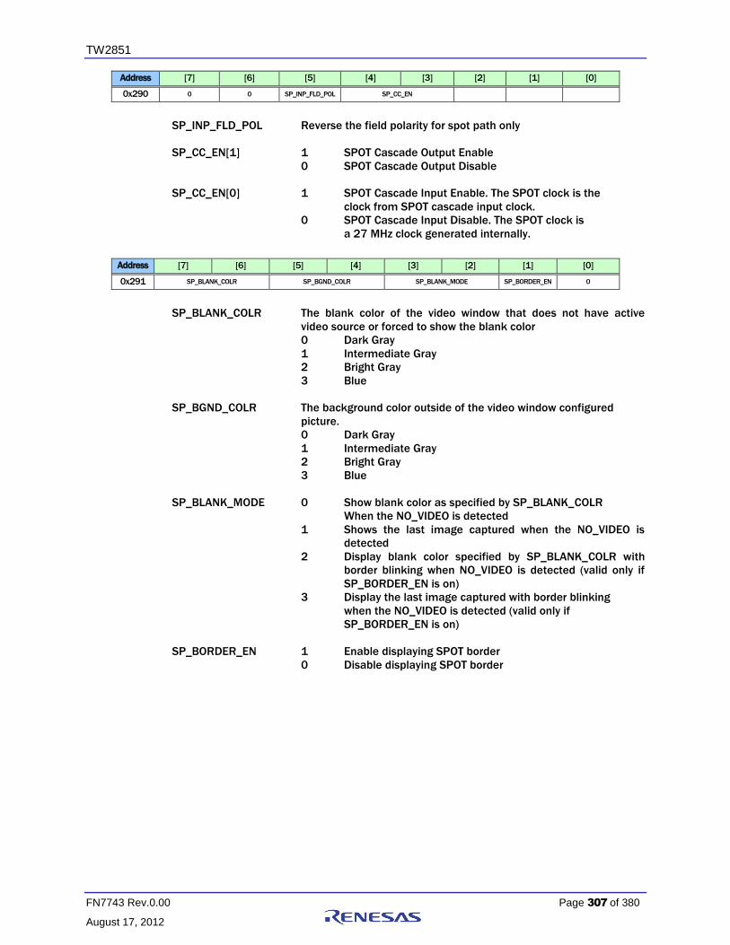
TW2851
FN7743 Rev.0.00 Page 307 of 380
August 17, 2012
Address [7] [6] [5] [4] [3] [2] [1] [0]
0x290 0 0 SP_INP_FLD_POL SP_CC_EN
SP_INP_FLD_POL Reverse the field polarity for spot path only
SP_CC_EN[1] 1 SPOT Cascade Output Enable
0 SPOT Cascade Output Disable
SP_CC_EN[0] 1 SPOT Cascade Input Enable. The SPOT clock is the
clock from SPOT cascade input clock.
0 SPOT Cascade Input Disable. The SPOT clock is
a 27 MHz clock generated internally.
Address [7] [6] [5] [4] [3] [2] [1] [0]
0x291 SP_BLANK_COLR SP_BGND_COLR SP_BLANK_MODE SP_BORDER_EN 0
SP_BLANK_COLR The blank color of the video window that does not have active
video source or forced to show the blank color
0 Dark Gray
1 Intermediate Gray
2 Bright Gray
3 Blue
SP_BGND_COLR The background color outside of the video window configured
picture.
0 Dark Gray
1 Intermediate Gray
2 Bright Gray
3 Blue
SP_BLANK_MODE 0 Show blank color as specified by SP_BLANK_COLR
When the NO_VIDEO is detected
1 Shows the last image captured when the NO_VIDEO is
detected
2 Display blank color specified by SP_BLANK_COLR with
border blinking when NO_VIDEO is detected (valid only if
SP_BORDER_EN is on)
3 Display the last image captured with border blinking
when the NO_VIDEO is detected (valid only if
SP_BORDER_EN is on)
SP_BORDER_EN 1 Enable displaying SPOT border
0 Disable displaying SPOT border

TW2851
FN7743 Rev.0.00 Page 308 of 380
August 17, 2012
Address [7] [6] [5] [4] [3] [2] [1] [0]
0x292 SP_BORDER_COLR 0 0 SP_LIM_656
SP_LIM_656 656 data value clamping selection
For Y
SP_LIM_656[2]
1 Maximum is 235
0 Maximum is 254
SP_LIM_656[1:0]
0 Minimum is 1
1 Minimum is 16,
2 Minimum is 24
3 Minimum is 32
For C
SP_LIM_656
0~1 Maximum 254, Minimum 1
2 ~ 7 Maximum 240, Minimum 16
SP_BORDER_COLR
0 Black
1 Dark gray
2 Light gray
3 White
Address [7] [6] [5] [4] [3] [2] [1] [0]
0x293 SP_H_OFFSET
0x294 0 SP_V_OFFSET
0x295 SP_H_SIZE[7:0]
0x296 SP_V_SIZE[7:0]
0x297 0 0 0 0 0 SP_V_SIZE[8] SP_H_SIZE[9:8]
SP_H_OFFSET The horizontal offset of the first active pixel in the output 656/601
format
SP_V_OFFSET The vertical offset of the first active line in the output 656/601
format
SP_H_SIZE The horizontal active length used to show the video pictures
SP_V_SIZE The vertical active height used to show the video pictures

TW2851
FN7743 Rev.0.00 Page 309 of 380
August 17, 2012
Address [7] [6] [5] [4] [3] [2] [1] [0]
0x298 SP_SQ_CMD SP_SQ_WR SP_SQ_RW_DONE* 0 0 0 0 SP_CONFIG_DONE
SP_SQ_CMD The command bit to start a SPOT Path Switch Queue read / write
operation. Set to 1 to start a command. This bit wills self clear.
SP_SQ_WR Read/Write Flag for SPOT Path Switch Queue operation
1 Write to Switch Queue
0 Read from Switch Queue
SP_SQ_RW_DONE Read Only
SP_CONFIG_DONE After any configuration changes are made to the control registers,
this bit should be set to resume the SPOT path operation.
Address [7] [6] [5] [4] [3] [2] [1] [0]
0x299 SP_SQ_ DATA[7:0]
0x29A SP_SQ_ DATA[15:8]
0x29B SP_SQ_ DATA[23:16]
SP_SQ_DATA are used to read/write the data from/to the SPOT path switch queue entry
when a switch queue read/write operation is performed.
In write operation, these 4 registers are written first. Then a command is issued using
SP_SQ_CMD in 0x298 to move the data into the switching queue.
In read operation, a read command is issued using SP_SQ_CMD in 0x298 to move the
data from switch queue into these 4 registers. The MCU can then read the entry from
these registers.
The definition of each bit used in the switch queue entry is as follows.
SP_SQ_DATA[1:0] Port ID for channel 0 (upper left window)
SP_SQ_DATA[3:2] Chip ID for channel 0
SP_SQ_DATA[5:4] Port ID for Channel 1 (upper right window)
SP_SQ_DATA[7:6] Chip ID for Channel 1
SP_SQ_DATA[9:8] Port ID for Channel 2 (Lower left window)
SP_SQ_DATA[11:10] Chip ID for Channel 2
SP_SQ_DATA[13:12] Port ID for Channel 3 (Lower right window)
SP_SQ_DATA[15:14] Chip ID for Channel 3
SP_SQ_DATA[19:16] Channel 0 ~ 3 disable bit.
Bit 16 set to 1, Channel 0 is disabled.
Bit 17 set to 1, Channel 1 is disabled
Bit 18 set to 1, Channel 2 is disabled
Bit 19 set to 1, Channel 3 is disabled
SP_SQ_DATA[22:20] Picture Type, as shown in Figure ??.
SP_SQ_DATA[23] Strobe field type for field mode picture type.
1 Odd field
0 Even field

TW2851
FN7743 Rev.0.00 Page 310 of 380
August 17, 2012
Address [7] [6] [5] [4] [3] [2] [1] [0]
0x29D SP_SQ_ ADDR
0x29E SP_SQ_ SIZE
SP_SQ_ADDR The switch queue entry address to perform the switch queue read /
write command. This address is automatically incremented after
the command is performed
SP_SQ_SIZE The switch queue size.
1 – 15: 1-15
16: 0
Address [7] [6] [5] [4] [3] [2] [1] [0]
0x2A0 SP_CH_EN_0 SP_FREEZE_0 SP_FUNC_MD_0 SP_ANA_0 0 SP_BLNK_0 SP_MIR_V_0 SP_MIR_H_0
0x2A1 SP_CH_EN_1 SP_FREEZE_1 SP_FUNC_MD_1 SP_ANA_1 0 SP_BLNK_1 SP_MIR_V_1 SP_MIR_H_1
0x2A2 SP_CH_EN_2 SP_FREEZE_2 SP_FUNC_MD_2 SP_ANA_2 0 SP_BLNK_2 SP_MIR_V_2 SP_MIR_H_2
0x2A3 SP_CH_EN_3 SP_FREEZE_3 SP_FUNC_MD_3 SP_ANA_3 0 SP_BLNK_3 SP_MIR_V_3 SP_MIR_H_3
SP_CH_EN Channel Enable Control for each of channel 0 through 3
1 Enable channel
0 Disable channel
SP_FREEZE 1 Freeze the video
0 Disable freeze
SP_FUNC_MD When the SPOT Path is not in Switch mode, this bit specifies the
SPOT mode of
1 Strobe Mode
0 Live Mode
SP_ANA Specify the analog input selection of each of the channel.
0 VINA
1 VINB
SP_BLNK Force the channel to display blank color
1 Blank Color
0 Normal video
SP_MIR_V Control to mirror the image vertically for each channel
0 Do not mirror vertically
1 Mirror vertically
SP_MIR_H Control to mirror the image horizontally for each channel
0 Do not mirror horizontally
1 Mirror horizontally
Address [7] [6] [5] [4] [3] [2] [1] [0]
0x2A4 0 0 0 0 SP_STROBE_3 SP_STROBE_2 SP_STROBE_1 SP_STROBE_0
SP_STROBE Strobe command for each channel. Once set to 1, the
corresponding channel will capture one field/frame and then clear
this bit.

TW2851
FN7743 Rev.0.00 Page 311 of 380
August 17, 2012
Address [7] [6] [5] [4] [3] [2] [1] [0]
0x2A5 0 SP_STRB_FLD SP_CH_CYCLE SP_SM_EN SP_PIC_TYPE
SP_STRB_FLD In non-switch mode, this bit controls which field to capture in field
mode ( pic_type 0, 2, 4, 6, 7)
0 Capture Even field
1 Capture Odd field
SP_CH_CYCLE In non-switch mode, this SP_CH_CYCLE controls how many
channels to interleave when the pic_type is 0, 1, 6, and 7.
PIC_TYPE 0, 1
0 Capture and interleave channel 0, 1, 2, 3
1 Capture channel 0
2 Capture and interleave channel 0, 1
3 Capture and interleave channel 0, 1, 2
PIC_TYPE 6, 7
1 Capture channel 0, 1
2 Capture and interleave channel 0, 1, 2, 3
SP_SM_EN 1 SPOT Path is in Switch Queue Mode
0 SPOT Path is in Live or Strobe Mode
SP_PIC_TYPE When SPOT Path is not in Switch Queue Mode, SP_PIC_TYPE
specifies the pic_type used in LIVE/Strobe mode
Address [7] [6] [5] [4] [3] [2] [1] [0]
0x2A6 SP_MOTN_ID_EN SP_DIG_ID_EN SP_ANA_ID_EN SP_ANA_RIC_EN SP_AUTO_ID_EN SP_AUTO_RPT_EN SP_DET_ID_EN SP_USR_ID_EN
SP_MOTN_ID_EN 1 Turn on motion information encoding
0 Do not turn on motion information encoding
SP_DIG_ID_EN 1 Turn on the digital channel ID encoding
0 Turn off the digital channel ID encoding
SP_ANA_ID_EN 1 Turn on the analog channel ID encoding
0 Turn off the analog channel ID encoding
SP_ANA_RPT_EN 1 Turn on the analog auto channel ID repeat line
0 Turn off the analog auto channel ID repeat line
SP_AUTO_ID_EN 1 Turn on the auto channel ID encoding
0 Turn off the auto channel ID encoding
SP_DET_ID_EN 1 Turn on the detection ID encoding
0 Turn off the detection ID encoding
SP_USR_ID_EN 1 Turn on the user information encoding
0 Turn off the user information encoding

TW2851
FN7743 Rev.0.00 Page 312 of 380
August 17, 2012
Address [7] [6] [5] [4] [3] [2] [1] [0]
0x2A7 SP_ANA_CHID_H_OFST
SP_ANA_CHID_H_OFST
The horizontal starting offset for Analog Channel ID
Address [7] [6] [5] [4] [3] [2] [1] [0]
0x2A8 SP_ANA_CHID_HIGH
0x2A9 SP_ANA_CHID_LOW
SP_ANA_CHID_HIGH Pixel values bigger than this setting are interpreted as “1” for
Analog Channel ID (default: 235)
SP_ANA_CHID_LOW Pixel values smaller than this setting are interpreted as “0” for
Analog Channel ID (default: 16)
Address [7] [6] [5] [4] [3] [2] [1] [0]
0x2AA SP_CHID_V_OFSTO 0 SP_CHID_V_OFST
0x2AB SP_CHID_V_OFSTE 0 SP_ANA_CHID_BW
SP_CHID_V_OFSTO Control the vertical starting offset on top of SP_CHID_V_OFST in
odd field for Analog Channel ID
SP_CHID_V_OFSTE Control the vertical starting offset on top of SP_CHID_V_OFST in
even field for Analog Channel ID
SP_CHID_V_OFST Vertical starting offset for Analog Channel ID. The actual vertical
line offset is SP_CHID_V_OFST + SP_CHID_V_OFSTO or
SP_CHID_V_OFST + SP_CHID_V_OFSTE
SP_ANA_CHID_BW Control the pixel width of each bit for Analog Channel ID
0 1 pixel
: :
31 32 pixels (default)
Address [7] [6] [5] [4] [3] [2] [1] [0]
0x2AC 0 0 0 0 0 0 0 SP_GEN_EN
SP_GEN_EN Internal Test Function
Default 0
Address [7] [6] [5] [4] [3] [2] [1] [0]
0x2AD SP_CHNUM1 SP_CHNUM0
0x2AE SP_CHNUM3 SP_CHNUM2
SP_CHNUM The Channel Number to display in non-switch mode
SP_CHNUMx[3:2]: CHIP ID
SP_CHNUMx[1:0]: PORT ID

TW2851
FN7743 Rev.0.00 Page 313 of 380
August 17, 2012
Address [7] [6] [5] [4] [3] [2] [1] [0]
0x2B0 SP_USER_CHID[7:0]
0x2B1 SP_USER_CHID[15:8]
0x2B2 SP_USER_CHID[23:16]
0x2B3 SP_USER_CHID[31:24]
0x2B4 SP_USER_CHID[39:32]
0x2B5 SP_USER_CHID[47:40]
0x2B6 SP_USER_CHID[55:48]
0x2B7 SP_USER_CHID[63:56]
SP_USER_CHID Used to set the USER Channel ID for SPOT path.
Address [7] [6] [5] [4] [3] [2] [1] [0]
0x2B8 SP_HALF_LINE[7:0]
0x2B9 SP_HALF_LINE[9:8] SP_HS_P_OS
0x2BA SP_HS_WIDTH
SP_HALF_LINE This defines in number of clock cycles from VS edge to the location
of field change, in case it is change in middle of a line
SP_HS_P_OS HSYNC starting location, in number of clock cycles
SP_HS_WIDTH HSYNC width, in number of clock cycles
Address [7] [6] [5] [4] [3] [2] [1] [0]
0x2BB 0 0 0 SP_TOP_VS_END
0x2BC 0 0 0 SP_BOT_VS_END
0x2BD SP_T_VS_POFS 0 0 SP_TOP_VS_OS
0x2BE SP_B_VS_POFS 0 0 SP_BOT_VS_OS
SP_TOP_VS_END VSYNC trailing edge location of top field, in number of lines
SP_BOT_VS_END VSYNC trailing edge location of bottom field, in number of lines
SP_TOP_VS_OS VSYNC leading edge location of top field, in number of lines
SP_BOT_VS_OS VSYNC leading edge location of bottom field, in number of lines
SP_T_VS_POS Enable the top field vsync edge at the middle of a line.
SP_B_VS_POS Enable the bottom field vsync edge at the middle of a line

TW2851
FN7743 Rev.0.00 Page 314 of 380
August 17, 2012
Address [7] [6] [5] [4] [3] [2] [1] [0]
0x2BF SP_HS_POL SP_VS_POL SP_FLD_POL SP_VAV_POL SP_HAV_POL SP_ 656_ERRCHK
SP_HS_POL Output HSYNC polarity control
SP_VS_POL Output VSYNC polarity control
SP_FLD_POL Output FIELD polarity control
SP_VAV_POL Output VAV polarity control
SP_HAV_POL Output HAV polarity control
SP_656_ERRCHK Enable 656 SAV/EAV error check
Address [7] [6] [5] [4] [3] [2] [1] [0]
0x2C0 SP_16
SP_16 16 Window Display Mode
Address [7] [6] [5] [4] [3] [2] [1] [0]
0x2C1 SP_16_WINNUM1 SP_16_WINNUM0
0x2C2 SP_16_WINNUM3 SP_16_WINNUM2
SP_16_WINNUM The window location of the 16 window configuration. The 16
windows are arranged as shown in the Figure 58.
Address [7] [6] [5] [4] [3] [2] [1] [0]
0x2C8 DP_HALF_LINE[7:0]
0x2C9 DP_HALF_LINE[9:8] DP_HS_P_OS
0x2CA DP_HS_WIDTH
DP_HALF_LINE This defines in number of clock cycles from VS edge to the location
of field change, in case it is change in middle of a line
DP_HS_P_OS HSYNC starting location, in number of clock cycles
DP_HS_WIDTH HSYNC width, in number of clock cycles

TW2851
FN7743 Rev.0.00 Page 315 of 380
August 17, 2012
Address [7] [6] [5] [4] [3] [2] [1] [0]
0x2CB DP_TOP_VS_END
0x2CC DP_BOT_VS_END
0x2CD DP_T_VS_POS DP_TOP_VS_OS
0x2CE DP_B_VS_POS DP_BOT_VS_OS
DP_TOP_VS_END VSYNC trailing edge location of top field, in number of lines
DP_BOT_VS_END VSYNC trailing edge location of bottom field, in number of lines
DP_TOP_VS_OS VSYNC leading edge location of top field, in number of lines
DP_BOT_VS_OS VSYNC leading edge location of bottom field, in number of lines
DP_T_VS_POS Enable the top field vsync edge at the middle of a line.
DP_B_VS_POS Enable the bottom field vsync edge at the middle of a line
Address [7] [6] [5] [4] [3] [2] [1] [0]
0x2CF DP_HS_POL DP_VS_POL DP_FLD_POL DP_VAV_POL DP_HAV_POL DP_656_ERRCHK
DP_HS_POL Output HSYNC polarity control
DP_VS_POL Output VSYNC polarity control
DP_FLD_POL Output FIELD polarity control
DP_VAV_POL Output VAV polarity control
DP_HAV_POL Output HAV polarity control
DP_656_ERRCHK Enable 656 SAV/EAV error check
Address [7] [6] [5] [4] [3] [2] [1] [0]
0x2D0 VE_FSCSEL 0 VE_FLD VE_VS 0 1 VE_PAL_NTSC
VE_FSCSEL Set the sub-carrier frequency for video encoder
0 3.57954545 MHz (default)
1 4.43361875 MHz
2 3.57561149 MHz
3 3.58205625 MHz
VE_FLD Define the field detection type
0 Use field from input field signal (default)
1 Detect field from combination of HSENC and VSENC
signals
VE_VS Define the vertical sync (VSYNC) detection type
0 Use signal from input VSYNC
1 Detect VSYNC from combination of HSENC and FLDEN
VE_PAL_NTSC Define the PAL or NTSC
0 NTSC
1 PAL
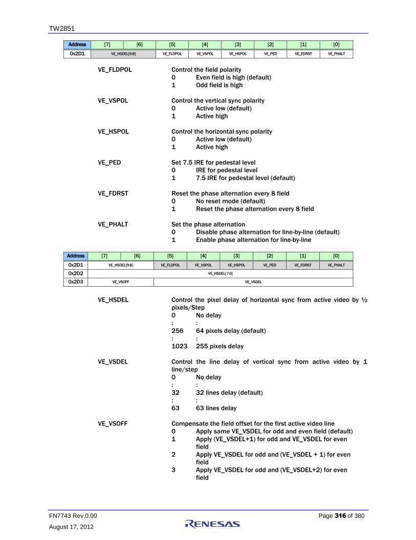
TW2851
FN7743 Rev.0.00 Page 316 of 380
August 17, 2012
Address [7] [6] [5] [4] [3] [2] [1] [0]
0x2D1 VE_HSDEL[9:8] VE_FLDPOL VE_VSPOL VE_HSPOL VE_PED VE_FDRST VE_PHALT
VE_FLDPOL Control the field polarity
0 Even field is high (default)
1 Odd field is high
VE_VSPOL Control the vertical sync polarity
0 Active low (default)
1 Active high
VE_HSPOL Control the horizontal sync polarity
0 Active low (default)
1 Active high
VE_PED Set 7.5 IRE for pedestal level
0 IRE for pedestal level
1 7.5 IRE for pedestal level (default)
VE_FDRST Reset the phase alternation every 8 field
0 No reset mode (default)
1 Reset the phase alternation every 8 field
VE_PHALT Set the phase alternation
0 Disable phase alternation for line-by-line (default)
1 Enable phase alternation for line-by-line
Address [7] [6] [5] [4] [3] [2] [1] [0]
0x2D1 VE_HSDEL[9:8] VE_FLDPOL VE_VSPOL VE_HSPOL VE_PED VE_FDRST VE_PHALT
0x2D2 VE_HSDEL[7:0]
0x2D3 VE_VSOFF VE_VSDEL
VE_HSDEL Control the pixel delay of horizontal sync from active video by ½
pixels/Step
0 No delay
: :
256 64 pixels delay (default)
: :
1023 255 pixels delay
VE_VSDEL Control the line delay of vertical sync from active video by 1
line/step
0 No delay
: :
32 32 lines delay (default)
: :
63 63 lines delay
VE_VSOFF Compensate the field offset for the first active video line
0 Apply same VE_VSDEL for odd and even field (default)
1 Apply (VE_VSDEL+1) for odd and VE_VSDEL for even
field
2 Apply VE_VSDEL for odd and (VE_VSDEL + 1) for even
field
3 Apply VE_VSDEL for odd and (VE_VSDEL+2) for even
field
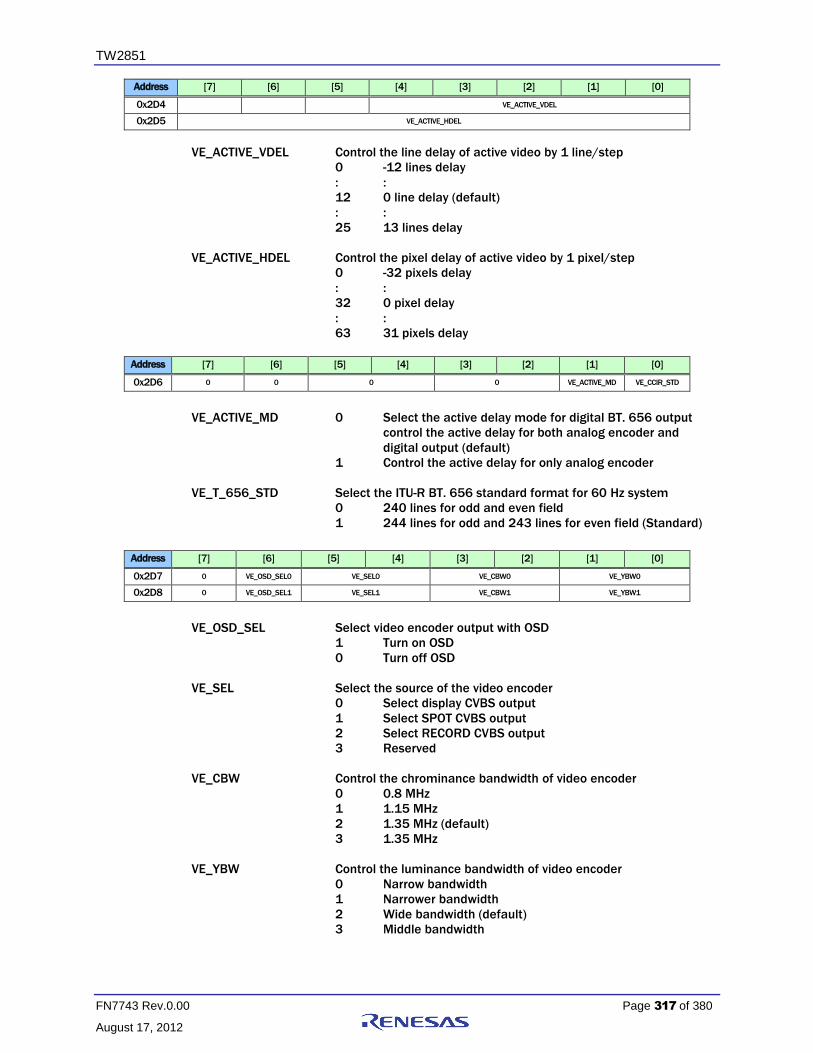
TW2851
FN7743 Rev.0.00 Page 317 of 380
August 17, 2012
Address [7] [6] [5] [4] [3] [2] [1] [0]
0x2D4 VE_ACTIVE_VDEL
0x2D5 VE_ACTIVE_HDEL
VE_ACTIVE_VDEL Control the line delay of active video by 1 line/step
0 -12 lines delay
: :
12 0 line delay (default)
: :
25 13 lines delay
VE_ACTIVE_HDEL Control the pixel delay of active video by 1 pixel/step
0 -32 pixels delay
: :
32 0 pixel delay
: :
63 31 pixels delay
Address [7] [6] [5] [4] [3] [2] [1] [0]
0x2D6 0 0 0 0 VE_ACTIVE_MD VE_CCIR_STD
VE_ACTIVE_MD 0 Select the active delay mode for digital BT. 656 output
control the active delay for both analog encoder and
digital output (default)
1 Control the active delay for only analog encoder
VE_T_656_STD Select the ITU-R BT. 656 standard format for 60 Hz system
0 240 lines for odd and even field
1 244 lines for odd and 243 lines for even field (Standard)
Address [7] [6] [5] [4] [3] [2] [1] [0]
0x2D7 0 VE_OSD_SEL0 VE_SEL0 VE_CBW0 VE_YBW0
0x2D8 0 VE_OSD_SEL1 VE_SEL1 VE_CBW1 VE_YBW1
VE_OSD_SEL Select video encoder output with OSD
1 Turn on OSD
0 Turn off OSD
VE_SEL Select the source of the video encoder
0 Select display CVBS output
1 Select SPOT CVBS output
2 Select RECORD CVBS output
3 Reserved
VE_CBW Control the chrominance bandwidth of video encoder
0 0.8 MHz
1 1.15 MHz
2 1.35 MHz (default)
3 1.35 MHz
VE_YBW Control the luminance bandwidth of video encoder
0 Narrow bandwidth
1 Narrower bandwidth
2 Wide bandwidth (default)
3 Middle bandwidth

TW2851
FN7743 Rev.0.00 Page 318 of 380
August 17, 2012
Address [7] [6] [5] [4] [3] [2] [1] [0]
0x2D9 VE_CBGEN1 VE_CKILL1 VE_CBGEN0 VE_CKILL0
VE_CBGEN Enable the test pattern output
0 Normal operation
1 Internal color bar with 100% amplitude and 100%
saturation
VE_CKILL Enable the color kill function
0 Normal operation (default)
1 Color is killed
Address [7] [6] [5] [4] [3] [2] [1] [0]
0x2DF AUX_DDR_DATA
AUX_DDR_DATA The data register used to read/write the internal 64 bytes FIFO
used to burst to/from the DDR
Address [7] [6] [5] [4] [3] [2] [1] [0]
0x2E0 AUX_DDR_ADDR[7:0]
0x2E1 AUX_DDR_ADDR[15:8]
0x2E2 AUX_DDR_ADDR[23:16]
AUX_DDR_ADDR The address registers used to burst read/write to/from DDR

TW2851
FN7743 Rev.0.00 Page 319 of 380
August 17, 2012
Address [7] [6] [5] [4] [3] [2] [1] [0]
0x2E3 AUX_DDR_LENGTH[7:0]
0x2E4 AUX_WAIT_POL AUX_DDR_LENGTH[10:8] AUX_FIFO_EMPTY* AUX_FIFO_FULL* AUX_DDR_RD AUX_DDR_WR
AUX_DDR_LENGTH Specify the length of the CPU burst read/write to/from DDR. The
Maximum length is 1204 bytes
AUX_WAIT_POL Reverse the polarity of the AUX WAIT signal
AUX_FIFO_EMPTY The internal 64 bytes FIFO emptiness status flag
1 The 64 bytes internal FIFO is empty and available
for writing data to burst to DDR
0 The 64 bytes internal FIFO is not empty, meaning
the previous move from FIFO to DDR is not
completed yet. The CPU should wait until this bit is
set before writing a new 64 bytes.
AUX_FIFO_FULL The internal 64 bytes FIFO has data available for CPU to read
This bit allows the CPU to poll after a AUX_DDR_RD command is
issued, or after every 64 bytes of data are read. With this bit set,
the CPU is safe to read up to 64 bytes, or up to the last burst
length derived from the AUX_DDR_LENGTH
1 The 64 bytes internal FIFO has some data
Available for CPU to read
0 The 64 bytes internal FIFO does not have data
for CPU to read yet
AUX_DDR_WR The AUX DDR Write Command. This bit is self-cleared
AUX_DDR_RD The AUX DDR Read Command. This bit is self-cleared.
Address [7] [6] [5] [4] [3] [2] [1] [0]
0x2E5 DDR_RD_CLK_SEL DDR_DQS_RD_DLY DDR_RD_TO_WR_NOP
DDR_RD_CLK_SEL Select the DQS or ~DQS as read clock to latch the DQ
DDR_DQS_RD_DLY Select the DQS valid read data cycle delay number
DDR_RD_TO_WR_NOP
DDR read to write adds additional nop cycles. Default 0

TW2851
FN7743 Rev.0.00 Page 320 of 380
August 17, 2012
Address [7] [6] [5] [4] [3] [2] [1] [0]
0x2E6 DDR_DQS_SEL0
0x2E7 DDR_DQS_SEL1
0x2E8 OSG_DDR_TIMER DDR_CLK90_SEL
DDR_DQS_SEL0 Select DDR_DQS_SEL/32 clock phase delay
DDR_DQS_SEL1 Select DDR_DQS_SEL/32 clock phase delay
DDR_CLK90_SEL Select the phase of 90 degree CLK generated from DLL.
The phase is DDR_CLK90_SEL/32
OSG_DDR_TIMER Timer to slow down the OSG write to avoid excessive peak
bandwidth
Address [7] [6] [5] [4] [3] [2] [1] [0]
0x2E9 DDR_DLL_TEST_SEL DDR_DLL_DEBUG_SEL DDR_DLL_TAP_S
DDR_DLL_DEBUG_SEL
Debug select to the DLL Debug Output
DDR_DLL_TEST_SEL Select the DLL test output signal
DDR_DLL_TAP_S Select the DLL TAPS
Address [7] [6] [5] [4] [3] [2] [1] [0]
0x2EA DDR_T_RC DDR_T_RAS
0x2EB DDR_T_RFC DDR_T_RP
0x2EC DDR_T_RCD DDR_T_WR
DDR_T_RC DDR t_rc timing
DDR_T_RAS DDR t_ras timing
DDR_T_RFC DDR t_rfc timing
DDR_T_RP DDR t_rp timing
DDR_T_RCD DDR t_rcd timing
DDR_T_WR DDR t_wr timing
Address [7] [6] [5] [4] [3] [2] [1] [0]
0x2ED DDR_REFRESH DDR_INIT_BYPASS DDR_B_LENGTH
DDR_REFRESH DDR refresh timing control
DDR_INIT_BYPASS DDR initialization bypass (for simulation purpose only)
DDR_B_LENGTH DDR burst length

TW2851
FN7743 Rev.0.00 Page 321 of 380
August 17, 2012
Address [7] [6] [5] [4] [3] [2] [1] [0]
0x2EE DDR_CAS_LAT DDR_SAMSUNG 0 DDR_SIZE
DDR_CAS_LAT DDR CAS Latency
DDR_SAMSUNG Internal test mode
DDR_SIZE
Address [7] [6] [5] [4] [3] [2] [1] [0]
0x2EF DDR_WTR DDR_B_TYPE DDR_DV_ST DDR_EN_DLL
DDR_WTR 1 DDR Write to Read Turn Around cycle needed
0 No Write to Read Turn Around cycle needed
DDR_B_TYPE External DDR Burst Type, for initialization use
DDR_DV_ST Configure external DDR driving strength, for initialization use
DDR_EN_DLL Enable the DLL in the external DDR memory, for initialization use
Address [7] [6] [5] [4] [3] [2] [1] [0]
0x2F0 SOFT_RSTN DLL_RST
SOFT_RSTN Software resetn signal for the whole chip. This bit does not reset
the configuration registers.
0 Reset
1 Release Reset
DLL_RST 1 Reset DLLs
0 Release Reset DLLs
Address [7] [6] [5] [4] [3] [2] [1] [0]
0x2F1 CHIP_ID
CHIP_ID Set the chip ID in cascade mode.
Address [7] [6] [5] [4] [3] [2] [1] [0]
0x2F5 SP_CC_CLK_SEL RP_CC_CLK_SEL 0 0 0 0
SP_CC_CLK_SEL [1] Reverse the SPOT output sampling across clock
domain from SCLK to CLKOS
[0] Reverse the SPOT input sampling across
clock domain from CLKIS to SCLK
RP_CC_CLK_SEL [1] Reverse the RECORD output sampling across clock
domain from RCLK to CLKOY
[0] Reverse the RECORD input sampling across clock
domain from CLKIY to RCLK

TW2851
FN7743 Rev.0.00 Page 322 of 380
August 17, 2012
Address [7] [6] [5] [4] [3] [2] [1] [0]
0x2F8 DP_CLK_CSCD_SEL DP_CLK_CSCD_PD CLKOX_SEL
DP_CLK_CSCD_SEL Select the clock source of the internal Display Cascade module
clock
0 54 MHz
1 27 MHz
2 108 MHz
3 PPLL clock output
DP_CLK_CSCD_PD Power down the display cascade clock
CLKOX_SEL Select the source of the display output CLKOX pin
0 From cascade clock as determined by
DP_CLK_CSCD_SEL
1 From 27 MHz Clock Source
Address [7] [6] [5] [4] [3] [2] [1] [0]
0x2FB CLKOY1_POL CLKOY0_POL CLKOS_POL CLKOX_POL
CLKOY1_POL Reverse the clock polarity of output CLKOY1 pin
CLKOY0_POL Reverse the clock polarity of output CLKOY0 pin
CLKOS_POL Reverse the clock polarity of the CLKOS pin
CLKOX_POL Reverse the clock polarity of the CLKOX pin
Address [7] [6] [5] [4] [3] [2] [1] [0]
0x2FC CLKIX_POL CLKPB_POL
CLKIX_POL Reverse the CLKIX polarity
CLKPB_POL Reverse the CLKPB polarity
Address [7] [6] [5] [4] [3] [2] [1] [0]
0x2FD CLKOS_DLY CLKOX_DLY
CLKOS_DLY Select the delay of CLKOS
CLKOX_DLY Select the delay of CLKOX
Address [7] [6] [5] [4] [3] [2] [1] [0]
0x2FE CLKOY1_DLY CLKOY0_DLY
CLKOY1_DLY Select the delay of CLKOY1
CLKOY0_DLY Select the delay of CLKOY0

TW2851
FN7743 Rev.0.00 Page 323 of 380
August 17, 2012
Page 3: 0x300 ~ 0x3FE
Address [7] [6] [5] [4] [3] [2] [1] [0]
0x301 0 BP_SCL_2S BP_SCL_2Y BP_SCL_2X 0 BP_SCL_1S BP_SCL_1Y BP_SCL_1X
0x302 0 BP_SCL_4S BP_SCL_4Y BP_SCL_4X 0 BP_SCL_3S BP_SCL_3Y BP_SCL_3X
BP_SCL_nX Bypass the down scaler of display path for port n
1 Bypass
0 Do not bypass
BP_SCL_nY Bypass the down scaler of record path for port n
1 Bypass
0 Do not bypass
BP_SCL_nS Bypass the down scaler of SPOT path for port n
1 Bypass
0 Do not bypass
Address [7] [6] [5] [4] [3] [2] [1] [0]
0x303 0 1 PTRN_LIM_656 PTRN_SMALL PTRN_CHIP_ID PTRN_PAL PTRN_EN
PTRN_LIM_656 Limit the pixel value generated by the internal pattern generator
after the video decoder.
1 Limit Y to 235 maximum, 16 minimum
0 Do not limit
PTRN_SMALL Internal pattern generator generates small frame. For simulation
only
PTRN_CHIP_ID Specify the chip ID of this chip
PTRN_PAL 1 Internal pattern generator generates PAL pattern
0 Internal pattern generator generates NTSC pattern
PTRN_EN Enable Internal pattern generator to replace the video stream
from video decoder
1 Enable the pattern generator
0 Use the video decoder input
Address [7] [6] [5] [4] [3] [2] [1] [0]
0x304 0 0 0 0 PTRN_VIDEO_LOSS
PTRN_VIDEO_LOSS Generate the video loss signal from the internal pattern
generator
1 Video Loss
0 Video detected
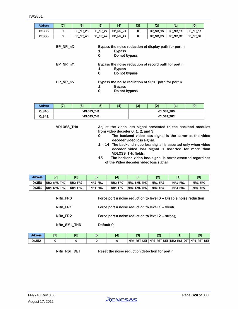
TW2851
FN7743 Rev.0.00 Page 324 of 380
August 17, 2012
Address [7] [6] [5] [4] [3] [2] [1] [0]
0x305 0 BP_NR_2S BP_NR_2Y BP_NR_2X 0 BP_NR_1S BP_NR_1Y BP_NR_1X
0x306 0 BP_NR_4S BP_NR_4Y BP_NR_4X 0 BP_NR_3S BP_NR_3Y BP_NR_3X
BP_NR_nX Bypass the noise reduction of display path for port n
1 Bypass
0 Do not bypass
BP_NR_nY Bypass the noise reduction of record path for port n
1 Bypass
0 Do not bypass
BP_NR_nS Bypass the noise reduction of SPOT path for port n
1 Bypass
0 Do not bypass
Address [7] [6] [5] [4] [3] [2] [1] [0]
0x340 VDLOSS_TH1 VDLOSS_TH0
0x341 VDLOSS_TH3 VDLOSS_TH2
VDLOSS_THn Adjust the video loss signal presented to the backend modules
from video decoder 0, 1, 2, and 3.
0 The backend video loss signal is the same as the video
decoder video loss signal.
1 – 14 The backend video loss signal is asserted only when video
decoder video loss signal is asserted for more than
VDLOSS_THx fields.
15 The backend video loss signal is never asserted regardless
of the Video decoder video loss signal.
Address [7] [6] [5] [4] [3] [2] [1] [0]
0x350 NR2_SML_THD NR2_FR2 NR2_FR1 NR2_FR0 NR1_SML_THD NR1_FR2 NR1_FR1 NR1_FR0
0x351 NR4_SML_THD NR4_FR2 NR4_FR1 NR4_FR0 NR3_SML_THD NR3_FR2 NR3_FR1 NR3_FR0
NRn_FR0 Force port n noise reduction to level 0 – Disable noise reduction
NRn_FR1 Force port n noise reduction to level 1 – weak
NRn_FR2 Force port n noise reduction to level 2 – strong
NRn_SML_THD Default 0
Address [7] [6] [5] [4] [3] [2] [1] [0]
0x352 0 0 0 0 NR4_RST_DET NR3_RST_DET NR2_RST_DET NR1_RST_DET
NRn_RST_DET Reset the noise reduction detection for port n

TW2851
FN7743 Rev.0.00 Page 325 of 380
August 17, 2012
Address [7] [6] [5] [4] [3] [2] [1] [0]
0x356 NR_DET_OUT_THD NR_DET_REF_VAR
NR_DET_OUT_THD Default 6
NR_DET_REF_VAR Default 1
Address [7] [6] [5] [4] [3] [2] [1] [0]
0x357 NR_DET_NOISE_1L
0x358 NR_DET_NOISE_1H
0x359 NR_DET_NOISE_2L
0x35A NR_DET_NOISE_2H
0x35B NR_DET_NOISE_CL
0x35C NR_DET_NOISE_CH
0x35D NR_DET_SKIP_L
0x35E NR_DET_SKIP_H
NR_DET_NOISE_1L Lower bound of pixel distance for noise level 1
Default: 3
NR_DET_NOISE_1H Higher bound of pixel distance for noise level 1
Default: 10
NR_DET_NOISE_2L Lower bound of pixel distance for noise level 2
Default: 5
NR_DET_NOISE_2H Higher bound of pixel distance for noise level 2
Default: 15
NR_DET_NOISE_CL Lower bound of pixel distance for chroma noise level
Default: 4
NR_DET_NOISE_CH Higher bound of pixel distance for chroma noise level
Default: 10
NR_DET_SKIP_L Pixels with value below this threshold will not be processed
Default: 25
NR_DET_SKIP_H Pixels with value above this threshold will not be processed
Default: 240
Address [7] [6] [5] [4] [3] [2] [1] [0]
0x35F NRDET4_LVL* NRDET3_LVL* NRDET2_LVL* NRDET1_LVL*
*Read only
NRDETn_LVL Detected noise level for channel n
0 Disable noise
1 Weak noise reduction
2 Strong noise reduction
Address [7] [6] [5] [4] [3] [2] [1] [0]

TW2851
FN7743 Rev.0.00 Page 326 of 380
August 17, 2012
0x380 HSCL_DISP_TARG_1
0x390 HSCL_DISP_TARG_2
0x3A0 HSCL_DISP_TARG_3
0x3B0 HSCL_DISP_TARG_4
HSCL_DISP_TARG_n The display down scaler target horizontal size for port n. The unit
is in multiple of 16 pixels
Address [7] [6] [5] [4] [3] [2] [1] [0]
0x381 VSCL_DISP_TARG_1
0x391 VSCL_DISP_TARG_2
0x3A1 VSCL_DISP_TARG_3
0x3B1 VSCL_DISP_TARG_4
VSCL_DISP_TARG_n The display down scaler target vertical size for port n. The unit is in
multiple of 8 lines
Address [7] [6] [5] [4] [3] [2] [1] [0]
0x382 HSCL_REC_TARG_1
0x392 HSCL_REC_TARG_2
0x3A2 HSCL_REC_TARG_3
0x3B2 HSCL_REC_TARG_4
HSCL_REC_TARG_n The record down scaler target horizontal size for port n. The unit
is in multiple of 16 pixels
Address [7] [6] [5] [4] [3] [2] [1] [0]
0x383 VSCL_REC_TARG_1
0x393 VSCL_REC_TARG_2
0x3A3 VSCL_REC_TARG_3
0x3B3 VSCL_REC_TARG_4
VSCL_REC_TARG_n The record down scaler target vertical size for port n. The unit is in
multiple of 8 lines
Address [7] [6] [5] [4] [3] [2] [1] [0]
0x384 HSCL_SPOT_TARG_1
0x394 HSCL_ SPOT _TARG_2
0x3A4 HSCL_ SPOT _TARG_3
0x3B4 HSCL_ SPOT _TARG_4
HSCL_SPOT_TARG_n The SPOT down scaler target horizontal size for port n. The unit
is in multiple of 16 pixels

TW2851
FN7743 Rev.0.00 Page 327 of 380
August 17, 2012
Address [7] [6] [5] [4] [3] [2] [1] [0]
0x385 VSCL_ SPOT _TARG_1
0x395 VSCL_ SPOT _TARG_2
0x3A5 VSCL_ SPOT _TARG_3
0x3B5 VSCL_ SPOT _TARG_4
VSCL_SPOT_TARG_n The SPOT down scaler target vertical size for port n. The unit is in
multiple of 8 lines
Address [7] [6] [5] [4] [3] [2] [1] [0]
0x387 HSCL_DISP_SRC_1
0x397 HSCL_DISP_ SRC _2
0x3A7 HSCL_DISP_ SRC _3
0x3B7 HSCL_DISP_ SRC _4
HSCL_DISP_SRC_n The display down scaler source horizontal size for port n. The unit is
in multiple of 16 pixels
Address [7] [6] [5] [4] [3] [2] [1] [0]
0x388 VSCL_DISP_SRC_1
0x398 VSCL_DISP_ SRC _2
0x3A8 VSCL_DISP_ SRC _3
0x3B8 VSCL_DISP_ SRC _4
VSCL_DISP_SRC_n The display down scaler source vertical size for port n. The unit is in
multiple of 8 lines
Address [7] [6] [5] [4] [3] [2] [1] [0]
0x389 HSCL_REC_ SRC _1
0x399 HSCL_REC_ SRC _2
0x3A9 HSCL_REC_ SRC _3
0x3B9 HSCL_REC_ SRC _4
HSCL_REC_SRC_n The record down scaler source horizontal size for port n. The unit is
in multiple of 16 pixels
Address [7] [6] [5] [4] [3] [2] [1] [0]
0x38A VSCL_REC_ SRC _1
0x39A VSCL_REC_ SRC _2
0x3AA VSCL_REC_ SRC _3
0x3BA VSCL_REC_ SRC _4
VSCL_REC_SRC_n The record down scaler source vertical size for port n. The unit is in
multiple of 8 lines

TW2851
FN7743 Rev.0.00 Page 328 of 380
August 17, 2012
Address [7] [6] [5] [4] [3] [2] [1] [0]
0x38B HSCL_SPOT_ SRC _1
0x39B HSCL_ SPOT _ SRC _2
0x3AB HSCL_ SPOT _ SRC _3
0x3BB HSCL_ SPOT _ SRC _4
HSCL_SPOT_SRC_n The SPOT down scaler source horizontal size for port n. The unit is
in multiple of 16 pixels
Address [7] [6] [5] [4] [3] [2] [1] [0]
0x38C VSCL_ SPOT _ SRC _1
0x39C VSCL_ SPOT _ SRC _2
0x3AC VSCL_ SPOT _ SRC _3
0x3BC VSCL_ SPOT _ SRC _4
VSCL_SPOT_SRC_n The SPOT down scaler source vertical size for port n. The unit is in
multiple of 8 lines
Address [7] [6] [5] [4] [3] [2] [1] [0]
0x386 FLDPOL_1S FLDPOL_1Y FLDPOL_1X
0x396 FLDPOL_2S FLDPOL_2Y FLDPOL_2X
0x3A6 FLDPOL_3S FLDPOL_3Y FLDPOL_3X
0x3B6 FLDPOL_4S FLDPOL_4Y FLDPOL_4X
FLDPOL_nX The display downscaler field polarity control for port n
FLDPOL_nY The record downscaler field polarity control for port n
FLDPOL_nS The SPOT downscaler field polarity control for port n
Page 4: 0x400 ~ 0x4FE
Address [7] [6] [5] [4] [3] [2] [1] [0]
0x480 VGA_RD_DIS VGA_RST
VGA_RST Software Reset for VGA / De-Interlacer / Brightness Control / RGB
control, timing generation modules. When this bit is set, the VGA
sync is lost.
VGA_RD_DIS Software Disable of the video buffer read side of the VGA path.
When this bit is set, the VGA output become blanks, and the VGA
sync is not lost. This bit can be set when the display configuration
change is performed.

TW2851
FN7743 Rev.0.00 Page 329 of 380
August 17, 2012
Address [7] [6] [5] [4] [3] [2] [1] [0]
0x488 GAMMA_ADDR[7:0]
0x489 GAMMA_ADDR[9:8]
0x48A GAMMA_WDATA[7:0]
0x48B GAMMA_WDATA[9:8]
0x48C GAMMA_RDATA[7:0]*
0x48D GAMMA_RDATA[9:8]*
0x48E GAMMA_RD_START
GAMMA_ADDR Gamma table address
GAMMA_WDATA Gamma table write data. The indirect write starts after writing
0x48B
GAMMA_RDATA Gamma table read data (Read Only)
GAMMA_RD_START Command to start a read by writing register 0x48E. Data written to
0x48E does not matter.
Address [7] [6] [5] [4] [3] [2] [1] [0]
0x490 M2DI_LOW_ANGLE_CNTL M2DI_USE_BOB
M2DI_LOW_ANGLE_CNTL
Disable a specific criterion to disqualify low angle. Default 0
M2DI_USE_BOB Use BOB instead of low angle. Default 0
Address [7] [6] [5] [4] [3] [2] [1] [0]
0x491 0 0 0 1 1 0 0 1
0x492 0 0 1 1 1 1 0 0
0x493 1 1 0 0 1 0 0 0
0x494 1 0 1 1 0 1 0 0
0x495 0 0 0 0 0 0 0 1
0x496 0 0 0 0 1 0 1 0
0x497 0 0 0 0 1 0 1 0
Reserved
Address [7] [6] [5] [4] [3] [2] [1] [0]
0x498 M2DI_FRM_WIDTH[7:0]
0x499 M2DI_FRM_PITCH[7:0]
0x49A M2DI_FRM_PITCH[10:8] M2DI_FRM_WIDTH[10:8]
0x49B M2DI_FRM_HEIGHT[7:0]
0x49C M2DI_FRM_HEIGHT[9:8]
M2DI_FRM_WIDTH The frame width of the incoming video in pixels
M2DI_FRM_PITCH The frame width allocated in the memory including the unused
portion at the end of each line
M2DI_FRM_HEIGHT The frame height of the incoming video in lines

TW2851
FN7743 Rev.0.00 Page 330 of 380
August 17, 2012
Address [7] [6] [5] [4] [3] [2] [1] [0]
0x4A0 UPS_BG_COLR
UPS_BG_COLR Background color used for UPS
Y = {UPS_BG_COLR[7:6], 6’b0}
Cb = {UPS_BG_COLR[5:3], 5’b0}
Cr = {UPS_BG_COLR[2:0], 5’b0}
Address [7] [6] [5] [4] [3] [2] [1] [0]
0x4A1 UPS_HST
0x4A2 UPS_VST
0x4A3 UPS_HACTIVE_O[7:0]
0x4A4 UPS_VACTIVE_O[7:0]
0x4A5 UPS_VACTIVE_O[10:8] UPS_HACTIVE_O[10:8]
UPS_HST Specify the video starting horizontal location in the output video
frame
UPS_VST Specify the video starting vertical location in the output video
frame
UPS_HACTIVE_O Specify the video width shown in the output video frame after
scaling
UPS_VACTIVE_O Specify the video height shown in the output video frame after
scaling
Address [7] [6] [5] [4] [3] [2] [1] [0]
0x4A8 UPS_HACTIVE_IN[7:0]
0x4A9 UPS_VACTIVE_IN[7:0]
0x4AA UPS_VACTIVE_IN[10:8] UPS_HACTIVE_IN[10:8]
UPS_HACTIVE_IN Specify the upscaler input horizontal video width
UPS_VACTIVE_IN Specify the upscaler input vertical video height
Address [7] [6] [5] [4] [3] [2] [1] [0]
0x4AB UPS_HSCALE[7:0]
0x4AC UPS_HSCALE[12:0]
0x4AD UPS_VSCALE[7:0]
0x4AE UPS_VSCALE[10:8]
UPS_HSCALE Horizontal scaling factor. 0x1000 represents scaling factor of 1
UPS_VSCALE Vertical scaling factor. 0x400 represents scaling factor of 1
Address [7] [6] [5] [4] [3] [2] [1] [0]
0x4AF VGA_BLACKOPUT
VGA_BLACKOUT 1 Black out the VGA output
0 Normal display

TW2851
FN7743 Rev.0.00 Page 331 of 380
August 17, 2012
Address [7] [6] [5] [4] [3] [2] [1] [0]
0x4B0 VGA_SHWIN VGA_SHCOR
0x4B1 VGA_OVERSHOOT VGA_SHARP
VGA_SHWIN[1] Sharpening filter window size selection
0 2 pixels
1 4 pixels
VGA_SHWIN[0] Sharpening filter min/max window size selection
0 2 pixels
1 4 pixels
VGA_SHCOR Sharpening Coring Setting
VGA_OVERSHOOT Sharpening overshoot setting
VGA_SHARP Sharpening gain
Address [7] [6] [5] [4] [3] [2] [1] [0]
0x4B2 VGA_BLACK
0x4B3 VGA_Y_GAIN
0x4B4 VGA_Y_OFFSET
0x4B5 VGA_CR_GAIN
0x4B6 VGA_CB_GAIN
VGA_BLACK The black level used for contrast control. Any incoming pixel less
than this value is assume to be black. The contrast control does
not amplify the black pixels.
VGA_Y_GAIN The contrast control. A setting of 64 represents gain of 1
(neutral)
VGA_Y_OFFSET The brightness control. A value of 128 represents offset of 0
(neutral)
VGA_CR_GAIN Cr gain control. A value of 64 represents gain of 1 (neutral)
VGA_CB_GAIN Cb gain control. A value of 64 represents gain of 1 (neutral)

TW2851
FN7743 Rev.0.00 Page 332 of 380
August 17, 2012
Address [7] [6] [5] [4] [3] [2] [1] [0]
0x4B7 VGA_BLKLVL VGA_WHTLVL VGA_HUEADJ
0x4B8 VGA_BWLST[7:0]
0x4B9 VGA_BWLEND[7:0]
0x4BA VGA_BWLEND[11:8] VGA_BWLST[11:8]
0x4BB VGA_BWFGAIN VGA_BWHGAIN
0x4BC VGA_BTILT
0x4BD VGA_WTILT
0x4BE VGA_BLIMIT
0x4BF VGA_WLIMIT
VGA_HUEADJ HUE Control
VGA_WHTLVL 0 235 as white
1 255 as white
VGA_BLKLVL 0 0 as black
1 16 as black
VGA_BWLST The first line of the black / white detection window for BW stretch
VGA_BWLEND The last line of the black / white detection window for BW stretch
VGA_BWHGAIN Tap for pixel recursive filtering before black / white line minmax
detection
VGA_BWFGAIN Tap for field recursive filtering before black / white field minmax
detection
VGA_BTILT Black Tilt point for BW stretch
VGA_WTILT White Tilt point for BW stretch
VGA_BLIMIT The darkest pixel value after BW stretch
VGA_WLIMIT The brightest pixel value after BW stretch

TW2851
FN7743 Rev.0.00 Page 333 of 380
August 17, 2012
Address [7] [6] [5] [4] [3] [2] [1] [0]
0x4C8 VGA_R_GAIN
0x4C9 VGA_R_OFFSET
0x4CA VGA_G_GAIN
0x4CB VGA_G_OFFSET
0x4CC VGA_B_GAIN
0x4CD VGA_B_OFFSET
VGA_R_GAIN Red color gain control. A setting of 64 represents gain of 1
(neutral)
VGA_R_OFFSET Red color offset control. A setting of 128 represents offset of 0
(neutral)
VGA_G_GAIN Green color gain control. A setting of 64 represents gain of 1
(neutral)
VGA_G_OFFSET Green color offset control. A setting of 128 represents offset of 0
(neutral)
VGA_B_GAIN Blue color gain control. A setting of 64 represents gain of 1
(neutral)
VGA_B_OFFSET Blue color offset control. A setting of 128 represents offset of 0
(neutral)
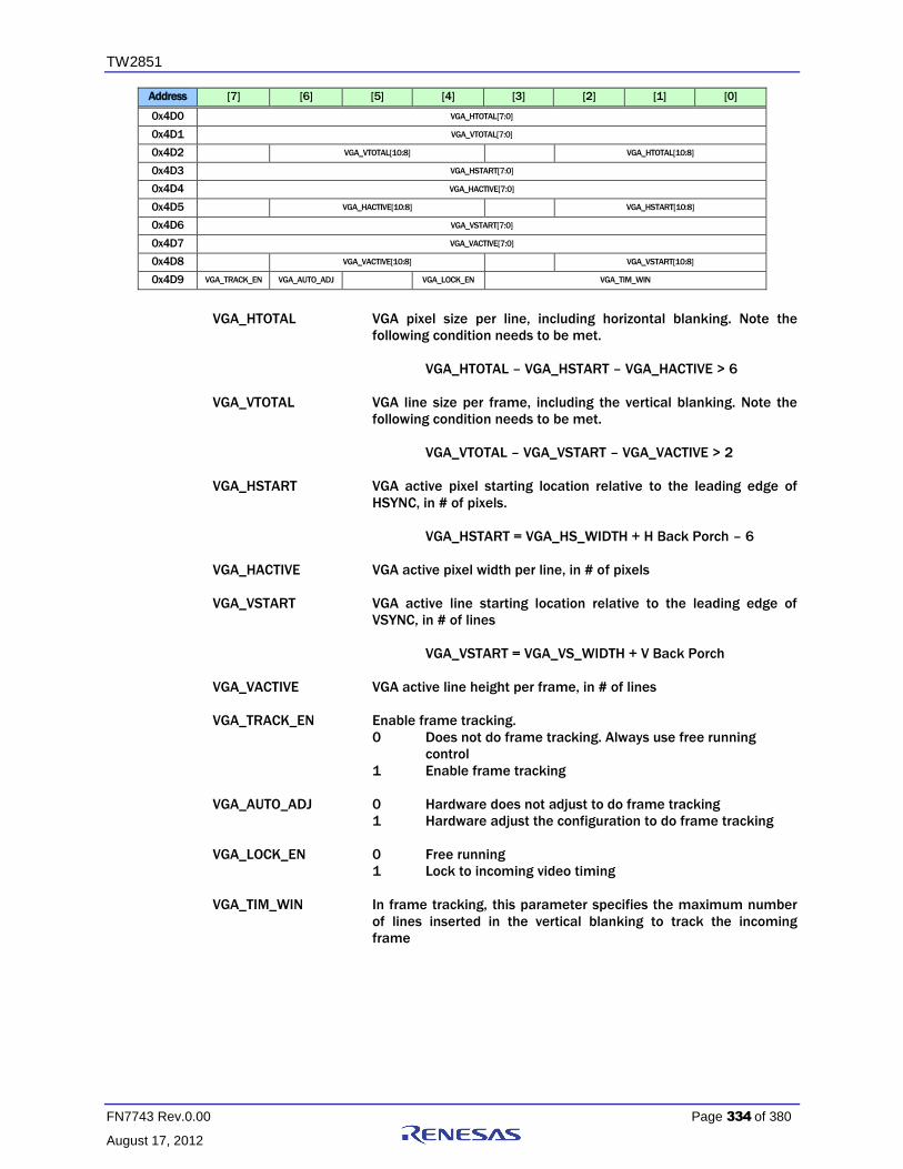
TW2851
FN7743 Rev.0.00 Page 334 of 380
August 17, 2012
Address [7] [6] [5] [4] [3] [2] [1] [0]
0x4D0 VGA_HTOTAL[7:0]
0x4D1 VGA_VTOTAL[7:0]
0x4D2 VGA_VTOTAL[10:8] VGA_HTOTAL[10:8]
0x4D3 VGA_HSTART[7:0]
0x4D4 VGA_HACTIVE[7:0]
0x4D5 VGA_HACTIVE[10:8] VGA_HSTART[10:8]
0x4D6 VGA_VSTART[7:0]
0x4D7 VGA_VACTIVE[7:0]
0x4D8 VGA_VACTIVE[10:8] VGA_VSTART[10:8]
0x4D9 VGA_TRACK_EN VGA_AUTO_ADJ VGA_LOCK_EN VGA_TIM_WIN
VGA_HTOTAL VGA pixel size per line, including horizontal blanking. Note the
following condition needs to be met.
VGA_HTOTAL – VGA_HSTART – VGA_HACTIVE > 6
VGA_VTOTAL VGA line size per frame, including the vertical blanking. Note the
following condition needs to be met.
VGA_VTOTAL – VGA_VSTART – VGA_VACTIVE > 2
VGA_HSTART VGA active pixel starting location relative to the leading edge of
HSYNC, in # of pixels.
VGA_HSTART = VGA_HS_WIDTH + H Back Porch – 6
VGA_HACTIVE VGA active pixel width per line, in # of pixels
VGA_VSTART VGA active line starting location relative to the leading edge of
VSYNC, in # of lines
VGA_VSTART = VGA_VS_WIDTH + V Back Porch
VGA_VACTIVE VGA active line height per frame, in # of lines
VGA_TRACK_EN Enable frame tracking.
0 Does not do frame tracking. Always use free running
control
1 Enable frame tracking
VGA_AUTO_ADJ 0 Hardware does not adjust to do frame tracking
1 Hardware adjust the configuration to do frame tracking
VGA_LOCK_EN 0 Free running
1 Lock to incoming video timing
VGA_TIM_WIN In frame tracking, this parameter specifies the maximum number
of lines inserted in the vertical blanking to track the incoming
frame
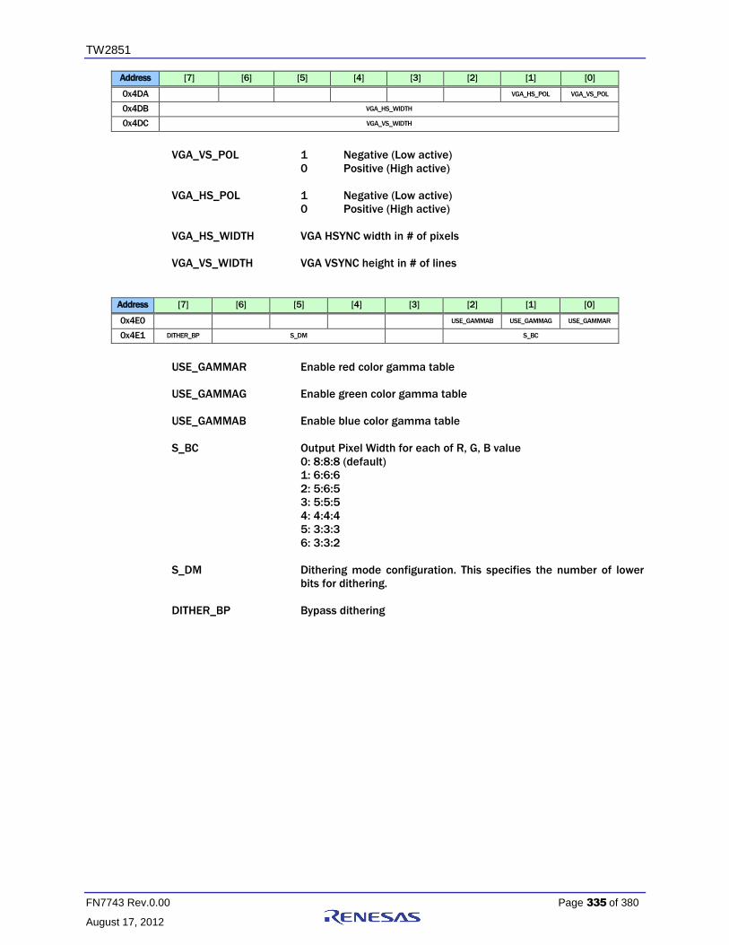
TW2851
FN7743 Rev.0.00 Page 335 of 380
August 17, 2012
Address [7] [6] [5] [4] [3] [2] [1] [0]
0x4DA VGA_HS_POL VGA_VS_POL
0x4DB VGA_HS_WIDTH
0x4DC VGA_VS_WIDTH
VGA_VS_POL 1 Negative (Low active)
0 Positive (High active)
VGA_HS_POL 1 Negative (Low active)
0 Positive (High active)
VGA_HS_WIDTH VGA HSYNC width in # of pixels
VGA_VS_WIDTH VGA VSYNC height in # of lines
Address [7] [6] [5] [4] [3] [2] [1] [0]
0x4E0 USE_GAMMAB USE_GAMMAG USE_GAMMAR
0x4E1 DITHER_BP S_DM S_BC
USE_GAMMAR Enable red color gamma table
USE_GAMMAG Enable green color gamma table
USE_GAMMAB Enable blue color gamma table
S_BC Output Pixel Width for each of R, G, B value
0: 8:8:8 (default)
1: 6:6:6
2: 5:6:5
3: 5:5:5
4: 4:4:4
5: 3:3:3
6: 3:3:2
S_DM Dithering mode configuration. This specifies the number of lower
bits for dithering.
DITHER_BP Bypass dithering

TW2851
FN7743 Rev.0.00 Page 336 of 380
August 17, 2012
Address [7] [6] [5] [4] [3] [2] [1] [0]
0x4E2 FP_PX_MODE FP_DE_AH FP_HS_AH FP_VS_AH FP_CK_AH
0x4E3 FP_SEL_LG FP_SIG_OFF FP_CKTPS
FP_PX_MODE 1 Set dual channel LVDS output
0 Set single channel LVDS output
FP_DE_AH 1 Panel DE signal active high
0 Panel DE signal active low
FP_HS_AH 1 Panel HS signal active high
0 Panel HS signal active low
FP_VS_AH 1 Panel VS signal active high
0 Panel VS signal active low
FP_CK_AH Reverse the FPCLK polarity
1 Data is sampled at the falling edge
0 Data is sampled at the rising edge
FP_SEL_LG 0 Select the LVDS mapping of the Samsung type
1 Select the LVDS mapping of the LG type
1 Reserved
2 Reserved
FP_SIG_OFF 0 Do not turn off the panel
1 Turn off the panel
FP_CKTPS Reserved

TW2851
FN7743 Rev.0.00 Page 337 of 380
August 17, 2012
Address [7] [6] [5] [4] [3] [2] [1] [0]
0x4E4 FP_PWR_CLK_DV
0x4E5 FP_CLK_PWDN FP_CLKSEL FP_MAN_PWR FP_EDPMS FP_PCR
FP_PWR_CLK_DV MSB of the internal 23 bit divide down counter. The 27 MHz clock
is divided by this counter to serve as the clock for Power State
Transition timer.
FP_CLK_PWDN 1 Force the internal panel clock to power down
FP_CLKSEL Default 1
FP_MAN_PWR Show current power management state. These power states
determine the states of FPPWC, FPBIAS, and FP Interfaces such as
FPVS, FPDE, FPCLK and all data signals.
FPPWC FPBIAS FP Interfaces
00: off “0” “0” “0”
01: Standby “1” “0” “0”
10: Suspend “1” “0” “1” or “0”
11: On “1” “1” “1” or “0”
The transition between power states does not occur right away. It
takes place after the timer expiration defined in 0x4E6 ~ 0x4E8
FP_EDPMS If FP_MAN_PWR is “0” and FP_EDPMS is “1”, it enables auto
power sequencing.
VSYNC loss & HSYNC loss Off
VSYNC loss & HSYNC active Standby
VSYNC active & HSYNC loss Suspend
VSYNC active & HSYNC active On
FP_PCR Force the power state to sequence to this state, and stay in this
state
0 Off
1 Standby
2 Suspend
3 On
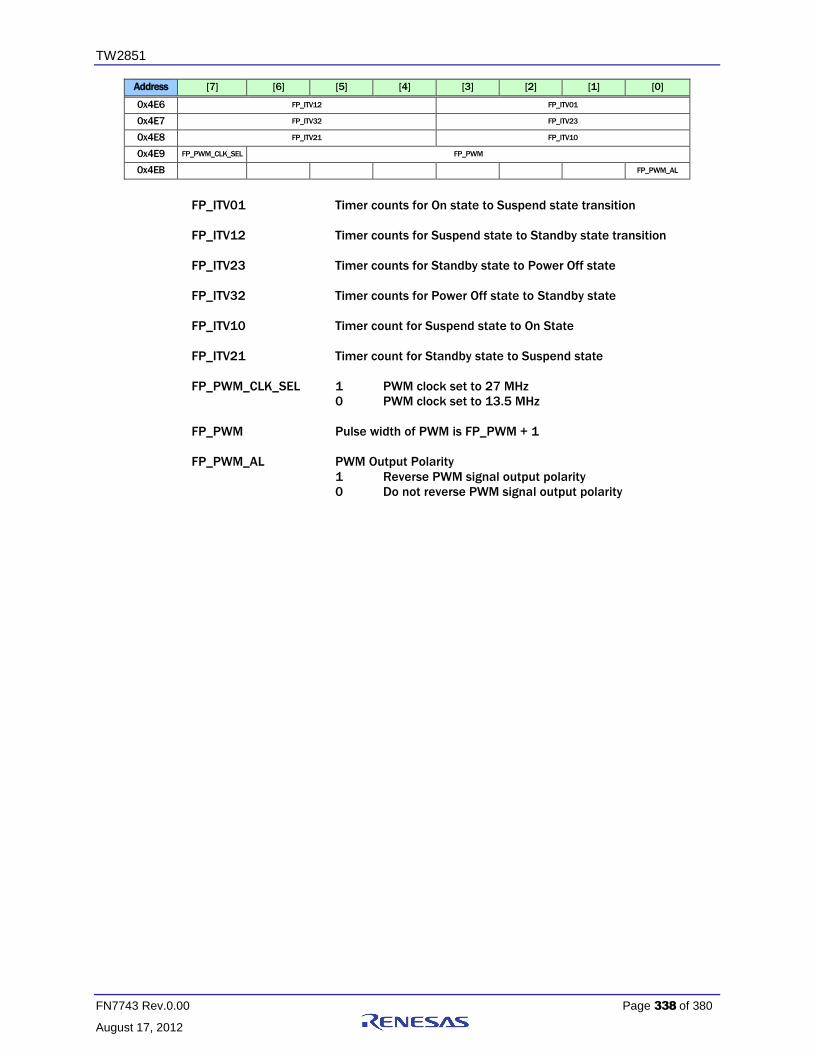
TW2851
FN7743 Rev.0.00 Page 338 of 380
August 17, 2012
Address [7] [6] [5] [4] [3] [2] [1] [0]
0x4E6 FP_ITV12 FP_ITV01
0x4E7 FP_ITV32 FP_ITV23
0x4E8 FP_ITV21 FP_ITV10
0x4E9 FP_PWM_CLK_SEL FP_PWM
0x4EB FP_PWM_AL
FP_ITV01 Timer counts for On state to Suspend state transition
FP_ITV12 Timer counts for Suspend state to Standby state transition
FP_ITV23 Timer counts for Standby state to Power Off state
FP_ITV32 Timer counts for Power Off state to Standby state
FP_ITV10 Timer count for Suspend state to On State
FP_ITV21 Timer count for Standby state to Suspend state
FP_PWM_CLK_SEL 1 PWM clock set to 27 MHz
0 PWM clock set to 13.5 MHz
FP_PWM Pulse width of PWM is FP_PWM + 1
FP_PWM_AL PWM Output Polarity
1 Reverse PWM signal output polarity
0 Do not reverse PWM signal output polarity

TW2851
FN7743 Rev.0.00 Page 339 of 380
August 17, 2012
Address [7] [6] [5] [4] [3] [2] [1] [0]
0x4F0 VGA_BYP_OSD VGA_BYP_DI VGA_DATA0 VGA_BYP_HUE VGA_BYP_YUV VGA_BYP_SHARP VGA_BYP_BW
0x4F2 VGA_BWGEN_PTRN VGA_BWGEN_EN VGA_CGEN_EN
VGA_BYP_OSD 1 Bypass OSD for the VGA path
0 Do not bypass OSD
VGA_BYP_DI 1 Bypass DI operation
0 Does not bypass DI
VGA_DATA0 1 Blank out the whole screen
0 Normal operation
VGA_BYP_HUE 1 Bypass Hue Control
0 Does not bypass Hue Control
VGA_BYP_YUV 1 Bypass YUV contrast / gain control
0 Does not bypass YUV contrast / gain control
VGA_BYP_SHARP 1 Bypass sharpness control
0 Does not bypass sharpness control
VGA_BYP_BW 1 Bypass black / white stretch control
0 Does not bypass black / white stretch control
VGA_BWGEN_PTRN Test pattern for internal use
0 Black / White Pattern
1 Color Pattern
2 Color Bar
3 Y Single line
4 Y block
5 BW pattern
6/7 Black
VGA_BWGEN_EN Pattern Generation Enable for Internal Test only
VGA_CGEN_EN Pattern Generation Enable for Internal use only
Address [7] [6] [5] [4] [3] [2] [1] [0]
0x4F3 VGA_DEBUG_DATA[7:4] VGA_DEBUG_DATA[3:0] * / VGA_DEBUG_SEL
VGA_DEBUG_SEL Write only. Set this to select the read back of register 0x4F0
VGA_DEBUG_DATA The setting of VGA_DEBUG_SEL determines the read back of this
register.
1 BWYMIN
2 BWYMAX
3 BWFMIN
4 BWFMAX
Others Not valid

TW2851
FN7743 Rev.0.00 Page 340 of 380
August 17, 2012
Page 5: 0x500 ~ 0x51F
Address [7] [6] [5] [4] [3] [2] [1] [0]
0x508 VDOX_BT1120_SEL VDOX_FLD_POL VDOX_1120_CROP VDOX_HVS_MD VDOX_DIG_OSD_BP DISP_CVBS_EN
DISP_CVBS_EN 1 Enable Display CVBS Path
0 Enable display digital output (either BT1120 or 8-bit
cascade)
VDOX_DIG_OSD_BP 1 Bypass the digital display path OSD
0 Enable the OSD on the display digital output
VDOX_HVS_MD 1 Output HAV/VAV signal at the HSYNC VSYNC port
0 Output regular HSYNC/VSYNC signal
VDOX_1120_CROP 1 BT1120 mode crop window enabled
0 BT1120 mode crop window disabled
VDOX_FLD_POL 1 Reverse the field polarity for display digital
output
0 Do not reverse the field polarity for display digital output
VDOX_BT1120_SEL 1 Select display digital output as the BT1120 output
0 Select display digital output as the 8-bit Cascade output
Address [7] [6] [5] [4] [3] [2] [1] [0]
0x509 VDOX_BT1120_TOP_OS[7:0]
0x50A VDOX_BT1120_BOT_OS[7:0]
0x50B VDOX_BT1120_L_OS[7:0]
0x50C VDOX_BT1120_R_OS[7:0]
0x50D VDOX_BT1120_R_OS[8] VDOX_BT1120_BOT_OS[8]
VDOX_BT1120_TOP_OS Top offset defining the vertical starting location
of active video in the BT1120 (1920x1080) frame
VDOX_BT1120_BOT_OS Bottom offset defining the vertical ending location of
active video in the BT1120 (1920x1080) frame
VDOX_BT1120_L_OS Left offset defining the horizontal starting location of
active video in the BT1120 (1920x1080) frame
VDOXD_BT1120_R_OS Right offset defining the horizontal ending location of
active video in the BT1120 (1920x1080) frame

TW2851
FN7743 Rev.0.00 Page 341 of 380
August 17, 2012
Address [7] [6] [5] [4] [3] [2] [1] [0]
0x50F VDOX_VAV_ODD_OFS
0x510 VDOX_VAV_EVEN_OFS
VDOX_VAV_ODD_OFS The line number between the beginning of the ODD field
and the beginning of VAV of display digital output
(BT1120 or cascade)
VDOX_VAV_EVEN_OFS The line number between the beginning of the EVEN field and the
beginning of VAV of display digital output (BT1120 or
cascade)
Address [7] [6] [5] [4] [3] [2] [1] [0]
0x511 VDOX_VS_POL VDOX_HS_POL VDOX_VS_ETP_EN VDOX_VS_ELP_EN VDOX_VS_OTP_EN VDOX_VS_OLP_EN
VDOX_VS_POL Select the VS polarity of display digital output.
1 Low active
0 High active
VDOX_HS_POL Select the HS polarity of display digital output
1 Low active
0 High active
VDOX_VS_ETP_EN Enable the pixel offset of even field VS trailing edge relative to HS
specified with VDOX_VS_POFS
VDOX_VS_ELP_EN Enable the pixel offset of even field VS leading edge relative to HS
specified with VDOX_VS_POFS
VDOX_VS_OTP_EN Enable the pixel offset of odd field VS trailing edge relative to HS
specified with VDOX_VS_POFS
VDOX_VS_OLP_EN Enable the pixel offset of odd field VS leading edge relative to HS
specified with VDOX_VS_POFS
Address [7] [6] [5] [4] [3] [2] [1] [0]
0x512 VDOX_VS_POFS[11:8] VDOX_VSYNC_WIDTH
0x513 VDOX_VS_POFS[7:0]
VDOX_VS_POFS The pixel offset of VS edge relative to HS for the display digital
output timing
VDOX_VSYNC_WIDTH The VSYNC width in unit of lines for the display digital output
timing
Address [7] [6] [5] [4] [3] [2] [1] [0]
0x514 VDOX_VS_E_LOFS VDOX_VS_O_LOFS
VDOX_VS_E_LOFS The even field line offset of the VS relative to the edge of field
change for the display digital output timing
VDOX_VS_O_LOFS The odd field line offset of the VS relative to the edge of field
change for the display digital output timing
Address [7] [6] [5] [4] [3] [2] [1] [0]

TW2851
FN7743 Rev.0.00 Page 342 of 380
August 17, 2012
0x515 VDOX_HS_WIDTH[8] 0
0x516 VDOX_HS_WIDTH[7:0]
0x517 0
VDOX_HS_WIDTH The HSYNC Width in number of pixels for the display digital output
timing
Address [7] [6] [5] [4] [3] [2] [1] [0]
0x518 VDOX_HACTIVE[11:8] VDOX_VACTIVE[9:8]
0x519 VDOX_VACTIVE[7:0]
0x51A VDOX_HACTIVE[7:0]
VDOX_HACTIVE The active pixels per line for the display digital output timing
VDOX_VACTIVE The active lines per field for the display digital output timing
Address [7] [6] [5] [4] [3] [2] [1] [0]
0x51B VDOX_OVT[9:8] VDOX_EVT[9:8]
0x51C VDOX_EVT[7:0]
0x51D VDOX_OVT[7:0]
VDOX_EVT The total line number of even field including vertical blanking for
the display digital output timing
VDOX_OVT The total line number of odd field including vertical blanking for the
display digital output timing
Address [7] [6] [5] [4] [3] [2] [1] [0]
0x51E VDOX_HT [11:8]
0x51F VDOX_HT [7:0]
VDOX_HT The total pixel number per line including horizontal blanking for the
display digital output timing
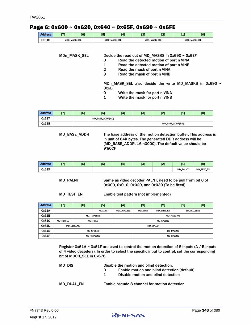
TW2851
FN7743 Rev.0.00 Page 343 of 380
August 17, 2012
Page 6: 0x600 ~ 0x620, 0x640 ~ 0x65F, 0x690 ~ 0x6FE
Address [7] [6] [5] [4] [3] [2] [1] [0]
0x616 MD3_MASK_SEL MD2_MASK_SEL MD1_MASK_SEL MD0_MASK_SEL
MDn_MASK_SEL Decide the read out of MD_MASKS in 0x690 ~ 0x6EF
0 Read the detected motion of port n VINA
1 Read the detected motion of port n VINB
2 Read the mask of port n VINA
3 Read the mask of port n VINB
MDn_MASK_SEL also decide the write MD_MASKS in 0x690 ~
0x6EF
0 Write the mask for port n VINA
1 Write the mask for port n VINB
Address [7] [6] [5] [4] [3] [2] [1] [0]
0x617 MD_BASE_ADDR[4:0]
0x618 MD_BASE_ADDR[8:5]
MD_BASE_ADDR The base address of the motion detection buffer. This address is
in unit of 64K bytes. The generated DDR address will be
{MD_BASE_ADDR, 16’h0000}. The default value should be
9’h0CF
Address [7] [6] [5] [4] [3] [2] [1] [0]
0x619 MD_PALNT MD_TEST_EN
MD_PALNT Same as video decoder PALNT, need to be pull from bit 0 of
0x000, 0x010, 0x020, and 0x030 (To be fixed)
MD_TEST_EN Enable test pattern (not implemented)
Address [7] [6] [5] [4] [3] [2] [1] [0]
0x61A MD_DIS MD_DUAL_EN MD_STRB MD_STRB_EN BD_CELLSENS
0x61B MD_TMPSENS MD_PIXEL_OS
0x61C MD_REFFLD MD_FIELD MD_LVSENS
0x61D MD_CELSENS MD_SPEED
0x61E MD_SPSENS BD_LVSENS
0x61F ND_TMPSENS ND_LVSENS
Register 0x61A ~ 0x61F are used to control the motion detection of 8 inputs (A / B inputs
of 4 video decoders). In order to select the specific input to control, set the corresponding
bit of MDCH_SEL in 0x676.
MD_DIS Disable the motion and blind detection.
0 Enable motion and blind detection (default)
1 Disable motion and blind detection
MD_DUAL_EN Enable pseudo 8 channel for motion detection
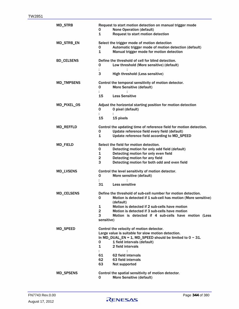
TW2851
FN7743 Rev.0.00 Page 344 of 380
August 17, 2012
MD_STRB Request to start motion detection on manual trigger mode
0 None Operation (default)
1 Request to start motion detection
MD_STRB_EN Select the trigger mode of motion detection
0 Automatic trigger mode of motion detection (default)
1 Manual trigger mode for motion detection
BD_CELSENS Define the threshold of cell for blind detection.
0 Low threshold (More sensitive) (default)
: :
3 High threshold (Less sensitive)
MD_TMPSENS Control the temporal sensitivity of motion detector.
0 More Sensitive (default)
: :
15 Less Sensitive
MD_PIXEL_OS Adjust the horizontal starting position for motion detection
0 0 pixel (default)
: :
15 15 pixels
MD_REFFLD Control the updating time of reference field for motion detection.
0 Update reference field every field (default)
1 Update reference field according to MD_SPEED
MD_FIELD Select the field for motion detection.
0 Detecting motion for only odd field (default)
1 Detecting motion for only even field
2 Detecting motion for any field
3 Detecting motion for both odd and even field
MD_LVSENS Control the level sensitivity of motion detector.
0 More sensitive (default)
: :
31 Less sensitive
MD_CELSENS Define the threshold of sub-cell number for motion detection.
0 Motion is detected if 1 sub-cell has motion (More sensitive)
(default)
1 Motion is detected if 2 sub-cells have motion
2 Motion is detected if 3 sub-cells have motion
3 Motion is detected if 4 sub-cells have motion (Less
sensitive)
MD_SPEED Control the velocity of motion detector.
Large value is suitable for slow motion detection.
In MD_DUAL_EN = 1, MD_SPEED should be limited to 0 ~ 31.
0 1 field intervals (default)
1 2 field intervals
: :
61 62 field intervals
62 63 field intervals
63 Not supported
MD_SPSENS Control the spatial sensitivity of motion detector.
0 More Sensitive (default)

TW2851
FN7743 Rev.0.00 Page 345 of 380
August 17, 2012
: :
15 Less Sensitive
BD_LVSENS Define the threshold of level for blind detection.
0 Low threshold (More sensitive) (default)
: :
15 High threshold (Less sensitive)
ND_TMPSENS Define the threshold of temporal sensitivity for night detection.
0 Low threshold (More sensitive) (default)
: :
15 High threshold (Less sensitive)
ND_LVSENS Define the threshold of level for night detection.
0 Low threshold (More sensitive) (default)
: :
15 High threshold (Less sensitive)
Address [7] [6] [5] [4] [3] [2] [1] [0]
0x620 0 0 BLINK_PERIOD
BLINK_PERIOD Define the blinking time from on to off and off to on
Address [7] [6] [5] [4] [3] [2] [1] [0]
0x640 OSG_MEM_WIDTH
OSG_MEM_WIDTH The OSG memory structure width in units of 64 pixels (128 bytes)
Address [7] [6] [5] [4] [3] [2] [1] [0]
0x641 OSG_WRBASE_ADDR
OSG_WRBASE_ADDR
The base address used for writing data into OSG memory
space. This base address can be set statically to treat all the
OSG memory space into a big one, or it can be set
dynamically to match each of the OSG base address at the
write side. The unit is in 64 Kbytes.
The DDR address generated from this register is
{1’b1, OSG_WRBASE_ADDR[7:0], 16’h0}

TW2851
FN7743 Rev.0.00 Page 346 of 380
August 17, 2012
Address [7] [6] [5] [4] [3] [2] [1] [0]
0x642 0 OSG_COLR_CON 0 1 1 OSG_OPMODE
OSG_COLR_CON 1 Turn on color conversion before writing into the
memory. There is a 4-entry color conversion table
used to match with the pixel value. If it matches,
the pixel is converted to a specified corresponding
output pixel value.
0 Turn off the color conversion function
OSG_OPMODE 0 Bitmap Write Mode – CPU fill all the pixel bitmaps
1 Block Move Mode – Move one block of memory
content from one location to another location
2 Block Fill Mode
3 Reserved
Address [7] [6] [5] [4] [3] [2] [1] [0]
0x645 OSG_SRC_SH[10:8] OSG_SRC_SV[10:8]
0x646 OSG_SRC_SV[7:0]
0x647 OSG_SRC_SH[7:0]
0x648 OSG_DST_EH[10:8] OSG_DST_EV[10:8]
0x649 OSG_DST_EV[7:0]
0x64A OSG_DST_EH[7:0]
0x64B OSG_DST_SH[10:8] OSG_DST_SV[10:8]
0x64C OSG_DST_SV[7:0]
0x64D OSG_DST_SH[7:0]
OSG_SRC_SV The start line of the source block
OSG_SRC_SH The starting pixel of the source block.
OSG_DST_EV The end line of the destination block
OSG_DST_EH The end pixel of the destination block
OSG_DST_SV The starting line of the destination block
OSG_DST_SH The starting pixel of the destination block.
Address [7] [6] [5] [4] [3] [2] [1] [0]
0x64E SELOSG 0 OSG_INDRD OSG_INDWR 0
OSG_INDWR Write 1 to start indirect write command for on-chip table selected
by OSG_SELOSG. Write only
OSG_INDRD Write 1 to start indirect read command from on-chip table selected
by OSG_SELOSG. Write only
OSG_SELOSG 0: Color conversion table.
Others: reserved.
Address [7] [6] [5] [4] [3] [2] [1] [0]
0x64F OSG_IDLE OSG_BMWR_BUSY OSG_OP_START
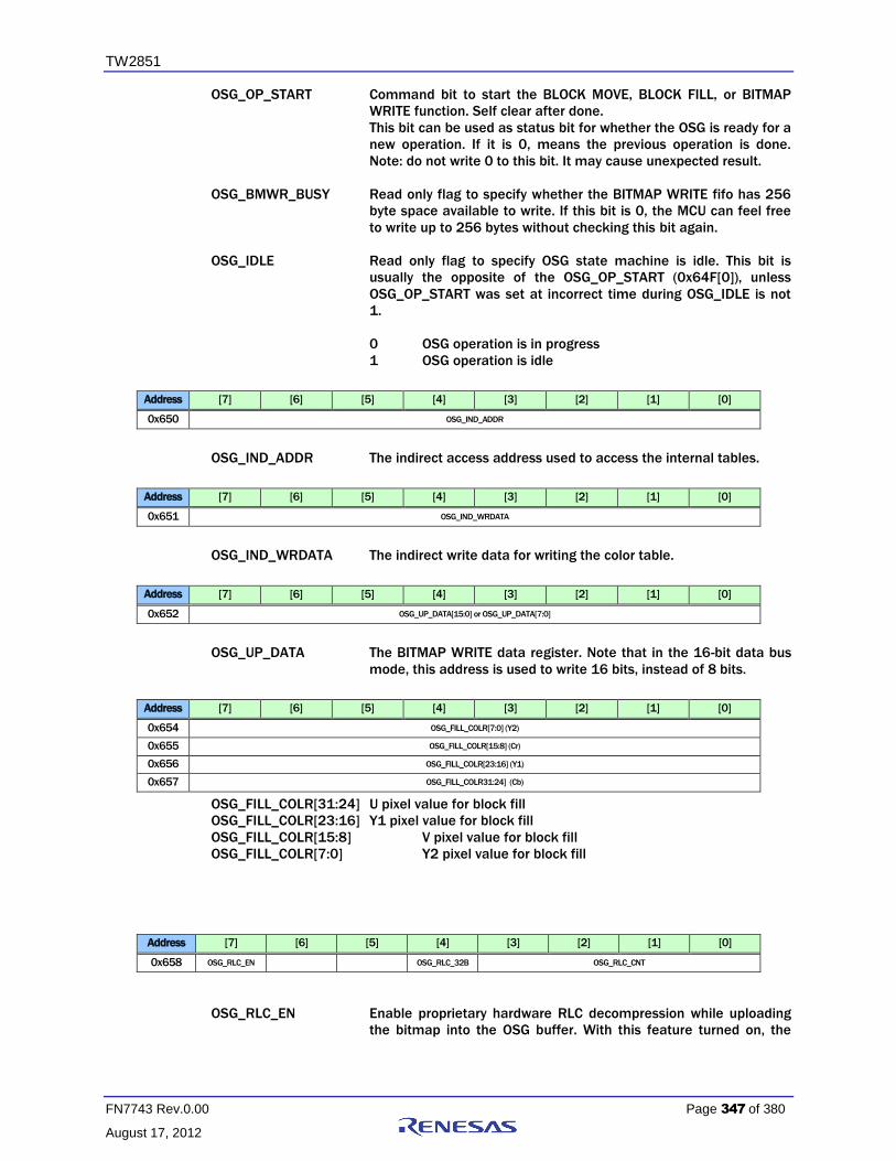
TW2851
FN7743 Rev.0.00 Page 347 of 380
August 17, 2012
OSG_OP_START Command bit to start the BLOCK MOVE, BLOCK FILL, or BITMAP
WRITE function. Self clear after done.
This bit can be used as status bit for whether the OSG is ready for a
new operation. If it is 0, means the previous operation is done.
Note: do not write 0 to this bit. It may cause unexpected result.
OSG_BMWR_BUSY Read only flag to specify whether the BITMAP WRITE fifo has 256
byte space available to write. If this bit is 0, the MCU can feel free
to write up to 256 bytes without checking this bit again.
OSG_IDLE Read only flag to specify OSG state machine is idle. This bit is
usually the opposite of the OSG_OP_START (0x64F[0]), unless
OSG_OP_START was set at incorrect time during OSG_IDLE is not
1.
0 OSG operation is in progress
1 OSG operation is idle
Address [7] [6] [5] [4] [3] [2] [1] [0]
0x650 OSG_IND_ADDR
OSG_IND_ADDR The indirect access address used to access the internal tables.
Address [7] [6] [5] [4] [3] [2] [1] [0]
0x651 OSG_IND_WRDATA
OSG_IND_WRDATA The indirect write data for writing the color table.
Address [7] [6] [5] [4] [3] [2] [1] [0]
0x652 OSG_UP_DATA[15:0] or OSG_UP_DATA[7:0]
OSG_UP_DATA The BITMAP WRITE data register. Note that in the 16-bit data bus
mode, this address is used to write 16 bits, instead of 8 bits.
Address [7] [6] [5] [4] [3] [2] [1] [0]
0x654 OSG_FILL_COLR[7:0] (Y2)
0x655 OSG_FILL_COLR[15:8] (Cr)
0x656 OSG_FILL_COLR[23:16] (Y1)
0x657 OSG_FILL_COLR31:24] (Cb)
OSG_FILL_COLR[31:24] U pixel value for block fill
OSG_FILL_COLR[23:16] Y1 pixel value for block fill
OSG_FILL_COLR[15:8] V pixel value for block fill
OSG_FILL_COLR[7:0] Y2 pixel value for block fill
Address [7] [6] [5] [4] [3] [2] [1] [0]
0x658 OSG_RLC_EN OSG_RLC_32B OSG_RLC_CNT
OSG_RLC_EN Enable proprietary hardware RLC decompression while uploading
the bitmap into the OSG buffer. With this feature turned on, the

TW2851
FN7743 Rev.0.00 Page 348 of 380
August 17, 2012
uploading bitmap from MCU through the host interface is in RLC
compressed format. The RLC compressed result is decompressed
by the hardware automatically. This reduces the bandwidth
consumption on the host interface.
OSG_RLC_32B 1 Use 32 bit data for compression pattern match
0 Use 16 bit data for compression pattern match
OSG_RLC_CNT Indicate how many bits are used for the repetition count.
0 The repetition count is 16 bits
1 – 15 The repetition count is 1 – 15 bits
The proprietary compression format is as follows:
F, D/C, F, D/C, …..
Where F (1 bit): 0 : indicate the following is pixel data
1 : indicate the following is repetition count
D : Pixel Data in either 16 bits or 32 bits, as specified by
OSG_RLC_32B)
C : Repetition count (how many times the D data is repeated. The
number of bits of this repetition count is controlled by the
OSG_RLC_CNT.
Note: count of 0 means 2**N repetition, where N is OSG_RLC_CNT
Address [7] [6] [5] [4] [3] [2] [1] [0]
0x65B CUR_EN
CUR_EN Enable the 5 OSD cursors. Only one of the 5 should be turned on.
Bit 0: Display VGA OSD
Bit 1: Display CVBS OSD
Bit 2: Record 0 OSD
Bit 3: Record 1 OSD
Bit 4: SPOT OSD

TW2851
FN7743 Rev.0.00 Page 349 of 380
August 17, 2012
Address [7] [6] [5] [4] [3] [2] [1] [0]
0x65C CUR_REV CUR_BLINK CUR_HOLLOW_OFF CUR_CUSTOM_LD CUR_SEL
CUR_REV Reverse the cursor color (black become white, white become
black)
CUR_BLINK Enable blink of mouse pointer.
0 Disable cursor blinking (default)
1 Enable cursor blinking
CUR_HOLLOW_OFF Control interior pixel color of the cursor.
0 Hollow cursor shape (only the border pixels are shown)
(default)
1 Filled with solid color specified by the cursor pixel
CUR_CUSTOM_LD Load the customized cursor shape from DDR memory into the on
chip SRAM
CUR_SEL Select the cursor type
0 Small cursor
1 Normal cursor
2 Customized cursor implemented with SRAM
3 Reserved
Address [7] [6] [5] [4] [3] [2] [1] [0]
0x65D CUR_Y[10:8] CUR_X[10:8]
0x65E CUR_X[7:0]
0x65F CUR_Y[7:0]
CUR_X Control the horizontal location of mouse pointer.
0 0 Pixel position (default)
: :
1440 1440 Pixel position
CUR_Y Control the vertical location of mouse pointer.
0 0 Line position (default)
: :
900 900 Line position

TW2851
FN7743 Rev.0.00 Page 350 of 380
August 17, 2012
Registers 0x690 ~ 0x6EF are used to control the mask of input A / B of each video decoder. To access the
corresponding inputs, set the corresponding MDn_MASK_SEL in 0x616.
Address [7] [6] [5] [4] [3] [2] [1] [0]
0x690 MD0_MASK0[7:0]
0x691 MD0_MASK0[15:8]
0x692 MD0_MASK1[7:0]
0x693 MD0_MASK1[15:8]
0x694 MD0_MASK2[7:0]
0x695 MD0_MASK2[15:8]
0x696 MD0_MASK3[7:0]
0x697 MD0_MASK3[15:8]
0x698 MD0_MASK4[7:0]
0x699 MD0_MASK4[15:8]
0x69A MD0_MASK5[7:0]
0x69B MD0_MASK5[15:8]
0x69C MD0_MASK6[7:0]
0x69D MD0_MASK6[15:8]
0x69E MD0_MASK7[7:0]
0x69F MD0_MASK7[15:8]
0x6A0 MD0_MASK8[7:0]
0x6A1 MD0_MASK8[15:8]
0x6A2 MD0_MASK9[7:0]
0x6A3 MD0_MASK9[15:8]
0x6A4 MD0_MASK10[7:0]
0x6A5 MD0_MASK10[15:8]
0x6A6 MD0_MASK11[7:0]
0x6A7 MD0_MASK11[15:8]
Address [7] [6] [5] [4] [3] [2] [1] [0]
0x6A8 MD1_MASK0[7:0]
0x6A9 MD1_MASK0[15:8]
0x6AA MD1_MASK1[7:0]
0x6AB MD1_MASK1[15:8]
0x6AC MD1_MASK2[7:0]
0x6AD MD1_MASK2[15:8]
0x6AE MD1_MASK3[7:0]
0x6AF MD1_MASK3[15:8]
0x6B0 MD1_MASK4[7:0]
0x6B1 MD1_MASK4[15:8]
0x6B2 MD1_MASK5[7:0]
0x6B3 MD1_MASK5[15:8]
0x6B4 MD1_MASK6[7:0]
0x6B5 MD1_MASK6[15:8]
0x6B6 MD1_MASK7[7:0]
0x6B7 MD1_MASK7[15:8]
0x6B8 MD1_MASK8[7:0]
0x6B9 MD1_MASK8[15:8]
0x6BA MD1_MASK9[7:0]
0x6BB MD1_MASK9[15:8]
0x6BC MD1_MASK10[7:0]
0x6BD MD1_MASK10[15:8]
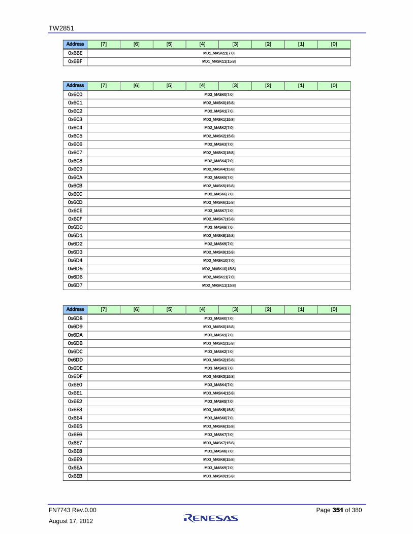
TW2851
FN7743 Rev.0.00 Page 351 of 380
August 17, 2012
Address [7] [6] [5] [4] [3] [2] [1] [0]
0x6BE MD1_MASK11[7:0]
0x6BF MD1_MASK11[15:8]
Address [7] [6] [5] [4] [3] [2] [1] [0]
0x6C0 MD2_MASK0[7:0]
0x6C1 MD2_MASK0[15:8]
0x6C2 MD2_MASK1[7:0]
0x6C3 MD2_MASK1[15:8]
0x6C4 MD2_MASK2[7:0]
0x6C5 MD2_MASK2[15:8]
0x6C6 MD2_MASK3[7:0]
0x6C7 MD2_MASK3[15:8]
0x6C8 MD2_MASK4[7:0]
0x6C9 MD2_MASK4[15:8]
0x6CA MD2_MASK5[7:0]
0x6CB MD2_MASK5[15:8]
0x6CC MD2_MASK6[7:0]
0x6CD MD2_MASK6[15:8]
0x6CE MD2_MASK7[7:0]
0x6CF MD2_MASK7[15:8]
0x6D0 MD2_MASK8[7:0]
0x6D1 MD2_MASK8[15:8]
0x6D2 MD2_MASK9[7:0]
0x6D3 MD2_MASK9[15:8]
0x6D4 MD2_MASK10[7:0]
0x6D5 MD2_MASK10[15:8]
0x6D6 MD2_MASK11[7:0]
0x6D7 MD2_MASK11[15:8]
Address [7] [6] [5] [4] [3] [2] [1] [0]
0x6D8 MD3_MASK0[7:0]
0x6D9 MD3_MASK0[15:8]
0x6DA MD3_MASK1[7:0]
0x6DB MD3_MASK1[15:8]
0x6DC MD3_MASK2[7:0]
0x6DD MD3_MASK2[15:8]
0x6DE MD3_MASK3[7:0]
0x6DF MD3_MASK3[15:8]
0x6E0 MD3_MASK4[7:0]
0x6E1 MD3_MASK4[15:8]
0x6E2 MD3_MASK5[7:0]
0x6E3 MD3_MASK5[15:8]
0x6E4 MD3_MASK6[7:0]
0x6E5 MD3_MASK6[15:8]
0x6E6 MD3_MASK7[7:0]
0x6E7 MD3_MASK7[15:8]
0x6E8 MD3_MASK8[7:0]
0x6E9 MD3_MASK8[15:8]
0x6EA MD3_MASK9[7:0]
0x6EB MD3_MASK9[15:8]

TW2851
FN7743 Rev.0.00 Page 352 of 380
August 17, 2012
Address [7] [6] [5] [4] [3] [2] [1] [0]
0x6EC MD3_MASK10[7:0]
0x6ED MD3_MASK10[15:8]
0x6EE MD3_MASK11[7:0]
0x6EF MD3_MASK11[15:8]
MDx_MASK Define the motion Mask/Detection cell for VIN x. MD_MASK[15] is
right end and
MD_MASK[0] is left end of column.
In writing mode
0 Non-masking cell for motion detection (default)
1 Masking cell for motion detection
In reading mode when MDn_MASK_SEL= “0”
0 Motion is not detected for cell
1 Motion is detected for cell
In reading mode when MDn_MASK_SEL= “1”
0 Non-masked cell
1 Masked cell
Address [7] [6] [5] [4] [3] [2] [1] [0]
0x6F0 MD_STRB_DET*
*Read only bit
MD_STRBn 1 MD strobe has been performed at channel n
0 MD strobe has not yet been performed at channel n
Address [7] [6] [5] [4] [3] [2] [1] [0]
0x6F1 NOVID_DET_0B* MD_DET_0B* BD_DET_0B* ND_DET_0B* NOVID_DET_0A* MD_DET_0A* BD_DET_0A* ND_DET_0A*
0x6F2 NOVID_DET_1B* MD_DET_1B* BD_DET_1B* ND_DET_1B* NOVID_DET_1A* MD_DET_1A* BD_DET_1A* ND_DET_1A*
0x6F3 NOVID_DET_2B* MD_DET_2B* BD_DET_2B* ND_DET_2B* NOVID_DET_2A* MD_DET_2A* BD_DET_2A* ND_DET_2A*
0x6F4 NOVID_DET_3B* MD_DET_3B* BD_DET_3B* ND_DET_3B* NOVID_DET_3A* MD_DET_3A* BD_DET_3A* ND_DET_3A*
*Read only bits
NOVID_DET_mA NO_VIDEO Detected from port m, analog path A (read only)
NOVID_DET_mB NO_VIDEO Detected from port m, analog path B (read only)
MD_DET_mA Motion Detected from port m, analog path A (read only)
MD_DET_mB Motion Detected from port m, analog path B (read only)
BD_DET_mA Blind Detected from port m, analog path A (read only)
BD_DET_mB Blind Detected from port m, analog path B (read only)
ND_DET_mA Night Detected from port m, analog path A (read only)
ND_DET_mB Night Detected from port m, analog path B

TW2851
FN7743 Rev.0.00 Page 353 of 380
August 17, 2012
Page 9: 0x9C0 ~ 0x9DF Address [7] [6] [5] [4] [3] [2] [1] [0]
0x9C0 DDC_FREQ_DIV[7:0]
0x9C1 DDC_FREQ_DIV[15:8]
DDC_FREQ_DIV DDC I2C Clock Generator generates DDC_CLK from an internal 54
MHz clock divided by DDC_FREQ_DIV.
Address [7] [6] [5] [4] [3] [2] [1] [0]
0x9C2 DDC_WR_DATA
DDC_WR_DATA DDC I2C Write Data Register
At the start operation, the content is as follows
Slave_Device_Addr DDC_WR_DATA[7:1]
R/W Command DDC_WR_DATA[0]
1 Read
0 Write
Address [7] [6] [5] [4] [3] [2] [1] [0]
0x9C3 DDC_RD_DATA
DDC_RD_DATA DDC I2C Read Data Register
Address [7] [6] [5] [4] [3] [2] [1] [0]
0x9C4 DDC_COMMAND
DDC_COMMAND DDC Control Command (Read/Write)
7 I2C Start
6 I2C Stop
5 Read the value from the slave device register.
Once acknowledged, the data will be in DDC_RD_DATA
register
4 Write the value in DDC_WR_DATA onto DDC_DATA bus
3 Send an ACK to the DDC_DATA bus when read
2 Clock Count Enable
1 Interrupt Enable
0 Interrupt Acknowledge

TW2851
FN7743 Rev.0.00 Page 354 of 380
August 17, 2012
Address [7] [6] [5] [4] [3] [2] [1] [0]
0x9C5 DDC_STATUS
DDC_STATUS DDC Status Register (read only)
Bit 7 RXACK
Bit 6 I2C_BUSY
Bit 5 Active Low
Bit 4 0
Bit 3 0
Bit 2 0
Bit 1 I2C Read/Write
Bit 0 Interrupt Acknowledge
Address [7] [6] [5] [4] [3] [2] [1] [0]
0x9C7 0
Reserved Should be kept 0
Address [7] [6] [5] [4] [3] [2] [1] [0]
0x9CF DDC_RST
DDC_RST DDC Software Reset whenever CPU issues a write to this address
Address [7] [6] [5] [4] [3] [2] [1] [0]
0x9D0 PS2_MaxNoSig PS2_MaxByte PS2_WR_EN PS2_EN
PS2_MaxNoSig Specify the length of time used to flag no signal when PS2_CK is
not toggled.
PS2_MaxByte Maximum number of bytes used in PS2 read operation from
PS2_D
PS2_WR_EN PS2 Data Write Enable to write data in PS2_WR_DATA onto PS2_D
PS2_EN PS2 Enable
Address [7] [6] [5] [4] [3] [2] [1] [0]
0x9D1 PS2_WR_DATA
PS2_WR_DATA Before writing this register, make sure the 0x9D0 control is written
with PS2_WR_EN = 1 and PS2_EN = 1.
Once writing into this register, the PS2 interface start sending
PS2_WR_DATA onto PS2_D bus.

TW2851
FN7743 Rev.0.00 Page 355 of 380
August 17, 2012
Address [7] [6] [5] [4] [3] [2] [1] [0]
0x9D2 PS2_RD_DATA[7:0]
0x9D3 PS2_RD_DATA[15:8]
0x9D4 PS2_RD_DATA[23:16]
0x9D5 PS2_RD_DATA[31:24]
PS2_RD_DATA Data read back from PS2 port. If PS2_WR_EN = 0, and PS2_EN =
1, and the PS2 Interrupt is asserted, the data on PS2_D bus are
available in these registers. The maximum number of valid bytes is
determined by PS2_MaxByte in 0x9D0
Address [7] [6] [5] [4] [3] [2] [1] [0]
0x9DF PS2_RST
PS2_RST PS2 Software Reset whenever CPU issues a write to this address
Page M: 0xM21 ~ 0xM3F, 0xM60 ~ 0xM8F, where M = 5 ~ 9
M=5: VGA OSD, M=6: Display CVBS OSD, M=7: REC0_OSD, M=8: REC1_OSD, M=9: SPOT_OSD
Address [7] [6] [5] [4] [3] [2] [1] [0]
0x521
0x621
0x721
0x821
0x921
0 0 OSD_FLD_POL OSD_VSYNC_POL
OSD_FLD_POL The Polarity control for the OSD to interpret the field signal
OSD_VSYNC_POL The polarity control for the OSD to interpret the VS when signal
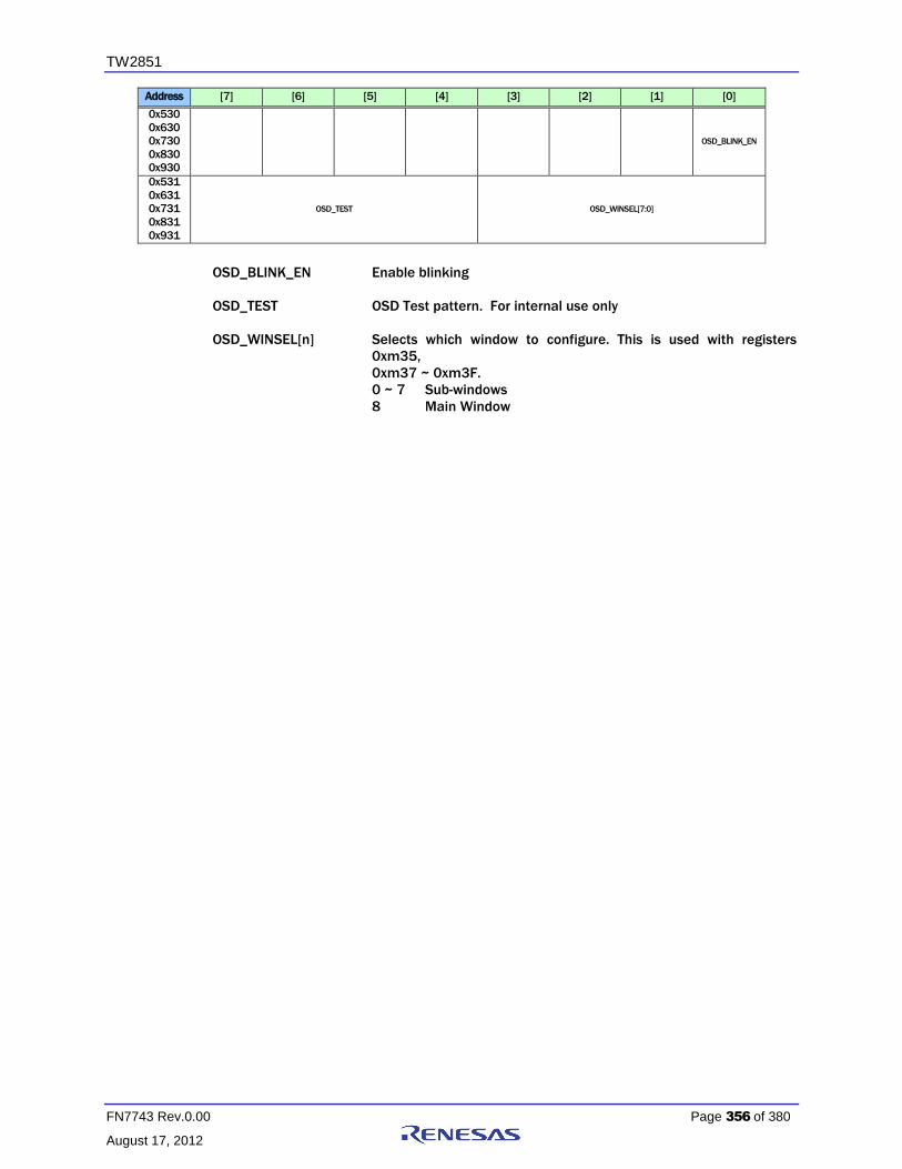
TW2851
FN7743 Rev.0.00 Page 356 of 380
August 17, 2012
Address [7] [6] [5] [4] [3] [2] [1] [0]
0x530
0x630
0x730
0x830
0x930
OSD_BLINK_EN
0x531
0x631
0x731
0x831
0x931
OSD_TEST OSD_WINSEL[7:0]
OSD_BLINK_EN Enable blinking
OSD_TEST OSD Test pattern. For internal use only
OSD_WINSEL[n] Selects which window to configure. This is used with registers
0xm35,
0xm37 ~ 0xm3F.
0 ~ 7 Sub-windows
8 Main Window
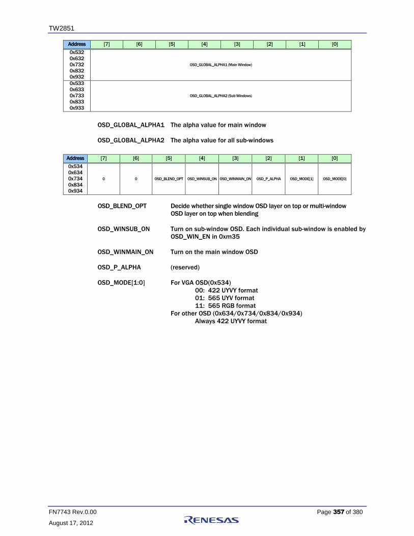
TW2851
FN7743 Rev.0.00 Page 357 of 380
August 17, 2012
Address [7] [6] [5] [4] [3] [2] [1] [0]
0x532
0x632
0x732
0x832
0x932
OSD_GLOBAL_ALPHA1 (Main Window)
0x533
0x633
0x733
0x833
0x933
OSD_GLOBAL_ALPHA2 (Sub Windows)
OSD_GLOBAL_ALPHA1 The alpha value for main window
OSD_GLOBAL_ALPHA2 The alpha value for all sub-windows
Address [7] [6] [5] [4] [3] [2] [1] [0]
0x534
0x634
0x734
0x834
0x934
0 0 OSD_BLEND_OPT OSD_WINSUB_ON OSD_WINMAIN_ON OSD_P_ALPHA OSD_MODE[1] OSD_MODE[0]
OSD_BLEND_OPT Decide whether single window OSD layer on top or multi-window
OSD layer on top when blending
OSD_WINSUB_ON Turn on sub-window OSD. Each individual sub-window is enabled by
OSD_WIN_EN in 0xm35
OSD_WINMAIN_ON Turn on the main window OSD
OSD_P_ALPHA (reserved)
OSD_MODE[1:0] For VGA OSD(0x534)
00: 422 UYVY format
01: 565 UYV format
11: 565 RGB format
For other OSD (0x634/0x734/0x834/0x934)
Always 422 UYVY format

TW2851
FN7743 Rev.0.00 Page 358 of 380
August 17, 2012
Address [7] [6] [5] [4] [3] [2] [1] [0]
0x535
0x635
0x735
0x835
0x935
OSD_BLINK_TIME OSD_WINSWITCH OSD_WINSET OSD_WIN_EN
OSD_BLINK_TIME Enable blinking of the window specified by OSD_WINSEL in 0xm31.
This bit is written into the corresponding window when
OSD_WINSET
is set to 1.
0 blink every 8 VSYNC
1 blink every 16 VSYNC
2 blink every 32 VSYNC
3 blink every 64 VSYNC
OSD_WINSWITCH Enable the dynamic field based OSD switching for record / SPOT
OSD
OSD_WINSET Write command to write to one of the 9 windows configuration
registers. This bit is not self cleared. It requires a clear before
setting to 1 again.
OSD_WIN_EN Enable the window specified by OSD_WINSEL in 0xm31. This bit is
written into the corresponding window when the OSD_WINSET is
set to 1.
Address [7] [6] [5] [4] [3] [2] [1] [0]
0x536
0x636
0x736
0x836
0x936
OSD_RDBASE_ADDR
OSD_RDBASE_ADDR The base address of the current OSD. Each OSD can have its own
base address. This address is in unit of 64 KB. The derived DDR
address will be { 1’b1, OSD_RDBASE_ADDR, 16’h0000 }

TW2851
FN7743 Rev.0.00 Page 359 of 380
August 17, 2012
Address [7] [6] [5] [4] [3] [2] [1] [0]
0x537
0x637
0x737
0x837
0x937
OSD_SRC_SH[11:8] OSD_SRC_SV[11:8]
0x538
0x638
0x738
0x838
0x938
OSD_SRC_SV[7:0]
0x539
0x639
0x739
0x839
0x939
OSD_SRC_SH[7:0]
0x53A
0x63A
0x73A
0x83A
0x93A
OSD_DST_EH[11:8] OSD_DST_EV[11:8]
0x53B
0x63B
0x73B
0x83B
0x93B
OSD_DST_EV[7:0]
0x53C
0x63C
0x73C
0x83C
0x93C
OSD_DST_EH[7:0]
0x53D
0x63D
0x73D
0x83D
0x93D
OSD_DST_SH[11:8] OSD_DST_SV[11:8]
0x53E
0x63E
0x73E
0x83E
0x93E
OSD_DST_SV[7:0]
0x53F
0x63F
0x73F
0x83F
0x93F
OSD_DST_SH[7:0]
The following register setting are saved into the corresponding OSD window specified by
OSD_WINSEL in 0xm31 when the OSD_WINSET bit is set to 1.
OSD_SRC_SV Starting line of the source block in the OSD memory
OSD_SRC_SH Starting pixel of the source block in the OSD memory
OSD_DST_EV Ending line of the OSD on the destination video stream
OSD_DST_EH End pixel location of the OSD on the destination video stream.
This should be the starting location OSD_DST_SH + OSD_WIDTH.
OSD_DST_SV Starting line of the OSD on the destination video stream
OSD_DST_SH Starting pixel location of the OSD on the destination video stream.

TW2851
FN7743 Rev.0.00 Page 360 of 380
August 17, 2012
Address [7] [6] [5] [4] [3] [2] [1] [0]
0x564
0x664
0x764
0x864
0x964
BOX1D_ALPHA1 BOX1D_ALPHA0
BOX1D_ALPHA0 The alpha value for the 6 1DBOXs below the bitmap OSG layer (1D
box 2 ~ 7)
BOX1D_ALPHA1 The alpha value for the 2 1DBOXs above the bitmap OSG layer
(1D box 0 ~ 1)
Address [7] [6] [5] [4] [3] [2] [1] [0]
0x566
0x666
0x766
0x866
0x966
MOSAIC_COLOR_SEL1 MOSAIC_COLOR_SEL0
MOSAIC_COLOR_SEL0
Mosaic color selection for the 6 1D Boxes below the bitmap
OSG layer
MOSAIC_COLOR_SEL1
Mosaic color selection for the 2 1D Boxes above the bitmap
OSG layer
0 White (75% Amplitude 100% Saturation)
1 Yellow (75% Amplitude 100% Saturation)
2 Cyan (75 % Amplitude 100 Saturation)
3 Green (75% Amplitude 100% Saturation)
4 Magenta (75% Amplitude 100% Saturation)
5 Red (75% Amplitude 100% Saturation)
6 Blue (75% Amplitude 100% Saturation)
7 0% Black
8 100% White
9 50% Gray
10 25% Gray
11 Blue (75% Amplitude 75% Saturation)
12 Defined by CLUT0 in 0xm78, 0xm7C, 0xm80
13 Defined by CLUT1 in 0xm79, 0xm7D, 0xm81
14 Defined by CLUT2 in 0xm7A, 0xm7E, 0xm82
15 Defined by CLUT3 in 0xm7B, 0xm7F, 0xm83
Address [7] [6] [5] [4] [3] [2] [1] [0]
0x567
0x667
0x767
0x867
0x967
BOX1D_EN
BOX1D_EN [1] Enable the upper layer with 2 Single Boxes
(1D Box 0 ~ 1)
[0] Enable the lower layer with 6 Single Boxes
(1D box 2 ~ 7)
Address [7] [6] [5] [4] [3] [2] [1] [0]
0x568
0x668
0x768
0x868
MOSAIC_EN BOX1D_MIX_EN BOX1D_BDR_EN BOX1D_INT_EN

TW2851
FN7743 Rev.0.00 Page 361 of 380
August 17, 2012
0x968
0x569
0x669
0x769
0x869
0x969
BOX1D_BDR_COLR BOX1D_COLR
0x56A
0x66A
0x76A
0x86A
0x96A
BOX1D_VT[9:8] BOX1D_HL[10:8]
0x56B
0x66B
0x76B
0x86B
0x96B
BOX1D_HL[7:0]
0x56C
0x66C
0x76C
0x86C
0x96C
BOX1D_VT[7:0]
0x56D
0x66D
0x76D
0x86D
0x96D
BOX1D_VW[9:8] BOX1D_HW[10:8]
0x56E
0x66E
0x76E
0x86E
0x96E
BOX1D_HW[7:0]
0x56F
0x66F
0x76F
0x86F
0x96F
BOX1D_VW[7:0]
Register 0xm68 ~ 0xm6F are used to control 8 sets of 1D-boxes. In order to access the 1D
box to control, use MDCH_SEL in 0xm76 to enable the corresponding bit before accessing
these registers.
MOSAIC_EN[m] Turn on the MOSAIC pattern in the 1D Box.
BOX1D_MIX_EN Transparent blending enable
BOX1D_ BDR_EN Enable showing the border line
BOX1D_INT_EN Enable showing the interior pixel color
BOX1D_BDR_COLR Define the box boundary color for each box
0 0% White (Default)
1 25% White
2 50% White
3 75% White
BOX1D_COLR Define the interior pixel colors
0 White (75% Amplitude 100% Saturation)
1 Yellow (75% Amplitude 100% Saturation)
2 Cyan (75 % Amplitude 100 Saturation)
3 Green (75% Amplitude 100% Saturation)
4 Magenta (75% Amplitude 100% Saturation)
5 Red (75% Amplitude 100% Saturation)
6 Blue (75% Amplitude 100% Saturation)
7 0% Black

TW2851
FN7743 Rev.0.00 Page 362 of 380
August 17, 2012
8 100% White
9 50% Gray
10 25% Gray
11 Blue (75% Amplitude 75% Saturation)
12 Defined by CLUT0 in 0xm78, 0xm7C, 0xm80
13 Defined by CLUT1 in 0xm79, 0xm7D, 0xm81
14 Defined by CLUT2 in 0xm7A, 0xm7E, 0xm82
15 Defined by CLUT3 in 0xm7B, 0xm7F, 0xm83
BOX1D_HL Define the horizontal left location of box.
0 Left end (default)
: :
1439 Right end
BOX1D_VT Define the vertical top location of box.
0 Vertical top (default)
: :
899 Vertical bottom
BOX1D_HW Define the horizontal size of box.
0 1 Pixel width (default)
: :
1439 1440 Pixels width
BOX1D_VW Define the vertical size of box.
0 1 Lines height (default)
: :
899 900 Lines height

TW2851
FN7743 Rev.0.00 Page 363 of 380
August 17, 2012
Address [7] [6] [5] [4] [3] [2] [1] [0]
0x575
0x675
0x775
0x875
0x975
MDBOX_EN MD_BND_MERG MDBOX_ALPHA
MDBOX_EN Enable the Motion 2D Box function
MD_BND_MERG Turn on the 2D Box merge if two adjacent box are both on
MDBOX_ALPHA Select the alpha blending mode for 2D arrayed Box
0 50% (default)
1 50%
2 75%
3 25%
Address [7] [6] [5] [4] [3] [2] [1] [0]
0x576
0x676
0x776
0x876
0x976
MDCH_SEL
MDCH_SEL Select one of the 8 1DBOXs to configure using 0xm68 ~ 0xm6F or
one of the 8 Motion 2D Boxes to configure using 0xm84 ~ 0xm8F.
Address [7] [6] [5] [4] [3] [2] [1] [0]
0x578
0x678
0x778
0x878
0x978
MD_CLUT0_Y
0x579
0x679
0x779
0x879
0x979
MD_CLUT1_Y
0x57A
0x67A
0x77A
0x87A
0x97A
MD_CLUT2_Y
0x57B
0x67B
0x77B
0x87B
0x97B
MD_CLUT3_Y
0x57C
0x67C
0x77C
0x87C
0x97C
MD_CLUT0_CB
0x57D
0x67D
0x77D
0x87D
0x97D
MD_CLUT1_CB
0x57E
0x67E
0x77E
0x87E
0x97E
MD_CLUT2_CB
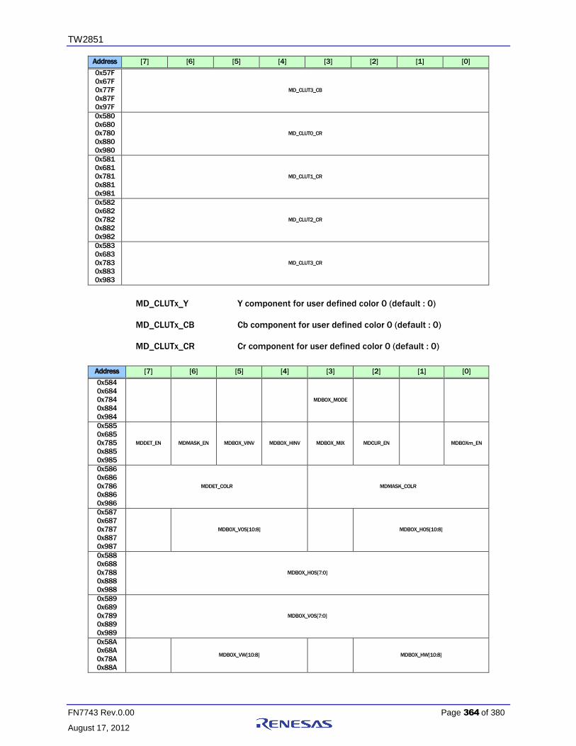
TW2851
FN7743 Rev.0.00 Page 364 of 380
August 17, 2012
Address [7] [6] [5] [4] [3] [2] [1] [0]
0x57F
0x67F
0x77F
0x87F
0x97F
MD_CLUT3_CB
0x580
0x680
0x780
0x880
0x980
MD_CLUT0_CR
0x581
0x681
0x781
0x881
0x981
MD_CLUT1_CR
0x582
0x682
0x782
0x882
0x982
MD_CLUT2_CR
0x583
0x683
0x783
0x883
0x983
MD_CLUT3_CR
MD_CLUTx_Y Y component for user defined color 0 (default : 0)
MD_CLUTx_CB Cb component for user defined color 0 (default : 0)
MD_CLUTx_CR Cr component for user defined color 0 (default : 0)
Address [7] [6] [5] [4] [3] [2] [1] [0]
0x584
0x684
0x784
0x884
0x984
MDBOX_MODE
0x585
0x685
0x785
0x885
0x985
MDDET_EN MDMASK_EN MDBOX_VINV MDBOX_HINV MDBOX_MIX MDCUR_EN MDBOXm_EN
0x586
0x686
0x786
0x886
0x986
MDDET_COLR MDMASK_COLR
0x587
0x687
0x787
0x887
0x987
MDBOX_VOS[10:8] MDBOX_HOS[10:8]
0x588
0x688
0x788
0x888
0x988
MDBOX_HOS[7:0]
0x589
0x689
0x789
0x889
0x989
MDBOX_VOS[7:0]
0x58A
0x68A
0x78A
0x88A
MDBOX_VW[10:8] MDBOX_HW[10:8]

TW2851
FN7743 Rev.0.00 Page 365 of 380
August 17, 2012
Address [7] [6] [5] [4] [3] [2] [1] [0]
0x98A
0x58B
0x68B
0x78B
0x88B
0x98B
MDBOX_HW[7:0]
0x58C
0x68C
0x78C
0x88C
0x98C
MDBOX_VW[7:0]
0x58D
0x68D
0x78D
0x88D
0x98D
MDBOX_BNDEN MD_BNDRY_COLR
0x58E
0x68E
0x78E
0x88E
0x98E
MDCUR_HPOS MDCUR_VPOS
0x58F
0x68F
0x78F
0x88F
0x98F
MDBOX_HCELL MDBOX_VCELL
Register 0xm84 ~ 0xm8F are used to control 8 sets of 2D boxes. In order to select the
specific 2D box to control, use MDCH_SEL in 0xm76 to enable the
corresponding bit before accessing these registers.
MDBOX_MODE Define the operation mode of 2D arrayed box.
0 Table mode (default)
1 Motion display mode
MDDET_EN Enable the motion cell display when the corresponding mask bit is
0
When MDBOX_MODE = “0”
0 Disable the detection plane of 2D arrayed box (default)
1 Enable the detection cell of 2D arrayed box
When MDBOX_MODE = “1”
0 Display the motion detection result with inner boundary
1 Display the motion detection result with whole cell area
MDMASK_EN Enable the mask plane of 2D arrayed box
0 Disable the mask plane of 2D arrayed box (default)
1 Enable the mask plane of 2D arrayed box
MDBOX_VINV Enable the vertical mirroring for 2D arrayed box.
0 Normal operation (default)
1 Enable the vertical mirroring
MDBOX_HINV Enable the horizontal mirroring for 2D arrayed box.
0 Normal operation (default)
1 Enable the horizontal mirroring
MDBOX_MIX Enable the alpha blending for 2D arrayed box plane with video
data.
0 Disable the alpha blending (default)
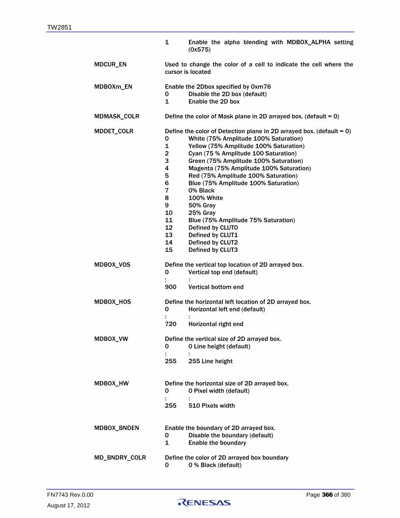
TW2851
FN7743 Rev.0.00 Page 366 of 380
August 17, 2012
1 Enable the alpha blending with MDBOX_ALPHA setting
(0x575)
MDCUR_EN Used to change the color of a cell to indicate the cell where the
cursor is located
MDBOXm_EN Enable the 2Dbox specified by 0xm76
0 Disable the 2D box (default)
1 Enable the 2D box
MDMASK_COLR Define the color of Mask plane in 2D arrayed box. (default = 0)
MDDET_COLR Define the color of Detection plane in 2D arrayed box. (default = 0)
0 White (75% Amplitude 100% Saturation)
1 Yellow (75% Amplitude 100% Saturation)
2 Cyan (75 % Amplitude 100 Saturation)
3 Green (75% Amplitude 100% Saturation)
4 Magenta (75% Amplitude 100% Saturation)
5 Red (75% Amplitude 100% Saturation)
6 Blue (75% Amplitude 100% Saturation)
7 0% Black
8 100% White
9 50% Gray
10 25% Gray
11 Blue (75% Amplitude 75% Saturation)
12 Defined by CLUT0
13 Defined by CLUT1
14 Defined by CLUT2
15 Defined by CLUT3
MDBOX_VOS Define the vertical top location of 2D arrayed box.
0 Vertical top end (default)
: :
900 Vertical bottom end
MDBOX_HOS Define the horizontal left location of 2D arrayed box.
0 Horizontal left end (default)
: :
720 Horizontal right end
MDBOX_VW Define the vertical size of 2D arrayed box.
0 0 Line height (default)
: :
255 255 Line height
MDBOX_HW Define the horizontal size of 2D arrayed box.
0 0 Pixel width (default)
: :
255 510 Pixels width
MDBOX_BNDEN Enable the boundary of 2D arrayed box.
0 Disable the boundary (default)
1 Enable the boundary
MD_BNDRY_COLR Define the color of 2D arrayed box boundary
0 0 % Black (default)
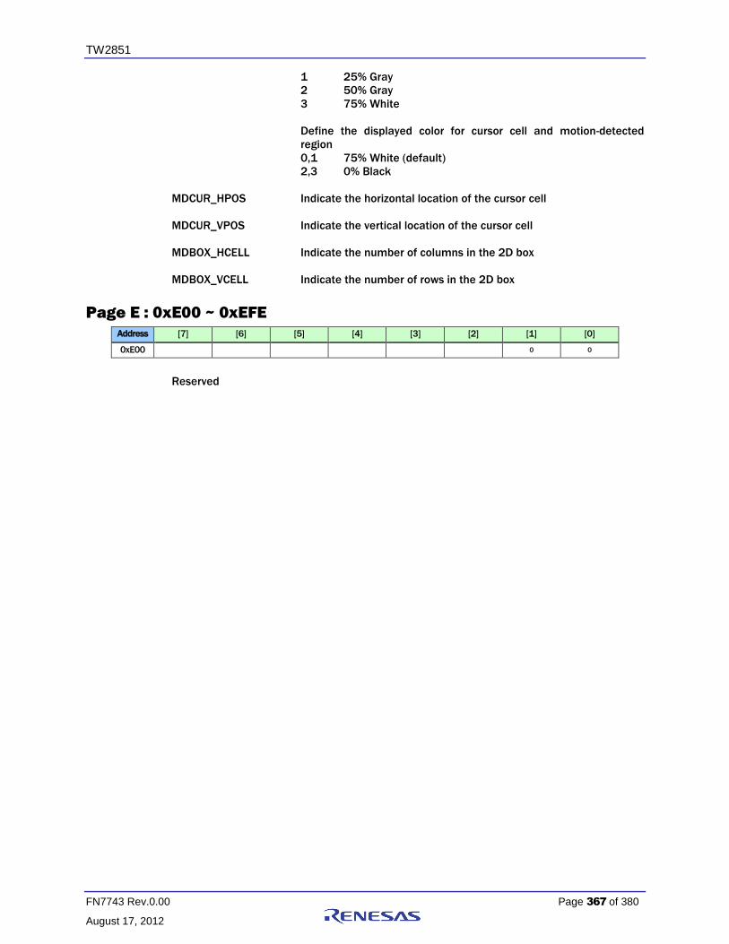
TW2851
FN7743 Rev.0.00 Page 367 of 380
August 17, 2012
1 25% Gray
2 50% Gray
3 75% White
Define the displayed color for cursor cell and motion-detected
region
0,1 75% White (default)
2,3 0% Black
MDCUR_HPOS Indicate the horizontal location of the cursor cell
MDCUR_VPOS Indicate the vertical location of the cursor cell
MDBOX_HCELL Indicate the number of columns in the 2D box
MDBOX_VCELL Indicate the number of rows in the 2D box
Page E : 0xE00 ~ 0xEFE
Address [7] [6] [5] [4] [3] [2] [1] [0]
0xE00 0 0
Reserved

TW2851
FN7743 Rev.0.00 Page 368 of 380
August 17, 2012
Address [7] [6] [5] [4] [3] [2] [1] [0]
0xE40 LVDS_LP_SEL LVDS_CP_SEL LVDS_EN LVDS_FAB_TEST LVDS_LCD_TEST
0xE41 LVDS_SWAP_CH LVDS_9BIT_DC LVDS_NS_SEL LVDS_DC_BAL LVDS_BITPERPIXEL LVDS_REV_DATA LVDS_SEL_LD
0xE42 LVDS_REV_DCB LVDS_DCB_POL LVDS_MAP_SEL
0xE43 LVDS_VOS_SEL LVDS_I_SEL
LVDS_LP_SEL Default 0
LVDS_CP_SEL Default 0
LVDS_EN 0 LVDS Disabled
1 LVDS Enabled
LVDS_FAB_TEST 0 Normal Operation
1 LVDS Test Mode
LVDS_LCD_TEST 0 Normal Operation
1 LCD Panel Test Mode
LVDS_SWAP_CH 1 Swap LVDS channel 0 and 1
0 Do not swap LVDS channel 0 and 1
LVDS_9BIT_DC 0 Select 7 cycle DC balance, as used in most National
chip
1 Select 9 cycle DC balance, as used in MAXIM chip
LVDS_NS_SEL 0 Output data mapping same as Maxim or THine LVDS
interface protocol
1 Output data mapping same as National interface
protocol
LVDS_DC_BAL 1 DC Balance Enable
0 DC Balance Disable
LVDS_BITPERPIXEL 0 6 bit data output
1 8 bit data output
2 10 bit data output
LVDS_REV_DATA 0 Normal data output format
1 Reverse data output format
LVDS_SEL_LD Load/Shift signal polarity selection
0 Active low
1 Active high
LVDS_REV_DCB 1 Reverse DC balance bit order
LVDS_DCB_POL 1 Reverse DC balance polarity
LVDS_MAP_SEL Change the mapping location of DE, VSYNC and HSYNC signals
000 {DE, VSYNC, HSYNC }
001 {VSYNC, HSYNC, DE }
010 {HSYNC, DE, VSYNC }
100 {DE, HSYNC, VSYNC }
101 {HSYNC, VSYNC, DE }
110 {VSYNC, DE, HSYNC }

TW2851
FN7743 Rev.0.00 Page 369 of 380
August 17, 2012
LVDS_VOS_SEL LVDS Driver Voltage Offset Select
LVDS_I_SEL LVDS Driver Output Swing Select
Address [7] [6] [5] [4] [3] [2] [1] [0]
0xEB0 PPLL_F[7:0]
0xEB1 PPLL_OD PPLL_R
0xEB2 EXT_PCLK_SEL PPLL_OE PPLL_BP
PPLL is controlled with the following equation
FOUT = (FIN * 2 * F) / (R * NO)
With the following restriction:
2 MHz < FIN / R < 8 MHz
200 MHz < FOUT * NO < 400 MHz
50 MHz < FOUT < 400 MHz
PPLL_F The F parameter in the equation
PPLL_R The R parameter in the equation
PPLL_OD OD of PLL, determines the NO in the equation
0 NOT ALLOWED
1 NO = 1
2 NO = 2
3 NO = 4
EXT_PCLK_SEL Select the external PCLK, rather than using the internal PLL Clock
3’b1xx Force pclk to 0
3’b000 Select PPLL_CLK
3’b010 Select PPLL_CLK/2
3’b0x1 Select P_EXT_PCLK
PPLL_OE OE of PCLK PLL
PPLL_BP Bypass of PCLK PLL

TW2851
FN7743 Rev.0.00 Page 370 of 380
August 17, 2012
Address [7] [6] [5] [4] [3] [2] [1] [0]
0xEB4 MPLL_F[7:0]
0xEB5 MPLL_F[8] MPLL_OD MPLL_R
0xEB6 EXT_MCLK_SEL MPLL_OE MPLL_BP
MPLL is controlled with the following equation
FOUT = (FIN * 2 * F) / (R * NO)
With the following restriction:
2 MHz < FIN / R < 8 MHz
200 MHz < FOUT * NO < 400 MHz
50 MHz < FOUT < 400 MHz
MPLL_F The F parameter in the equation
MPLL_R The R parameter in the equation
MPLL_OD OD of PLL, determines the NO in the equation
0 Not allowed
1 NO = 1
2 NO = 2
3 NO = 4
EXT_MCLK_SEL 1 Select the external MCLK signal rather than from PLL
0 Select the PLL output as MCLK
MPLL_OE OE of MPLL
MPLL_BP Bypass of MPLL
Address [7] [6] [5] [4] [3] [2] [1] [0]
0xEB8 SPLL_IREF SPLL_CPX4 SPLL_LPX4
SPLL_IREF System clock PLL current control
0 Lower current (Default)
1 Higher current (30% more than setting to 0)
SPLL_CPX4 System clock PLL charge pump select
0 1 uA
1 5 uA (Default)
2 10 uA
3 15 uA
SPLL_LPX4 System clock PLL loop filter select
0 80K Ohms
1 40K Ohms (Default)
2 30K Ohms
3 20K Ohms
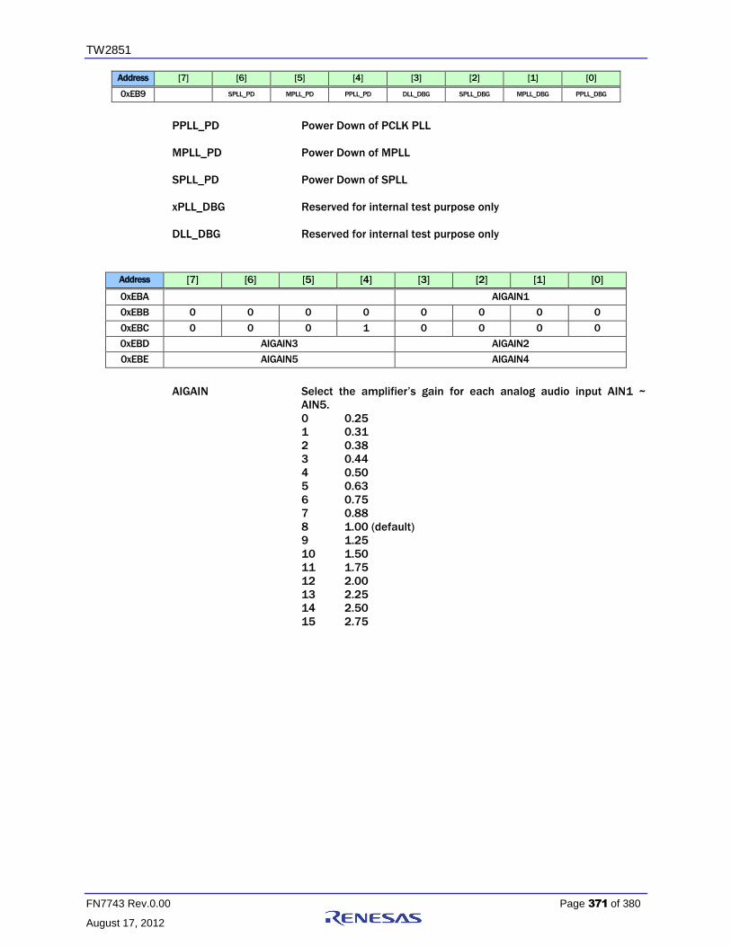
TW2851
FN7743 Rev.0.00 Page 371 of 380
August 17, 2012
Address [7] [6] [5] [4] [3] [2] [1] [0]
0xEB9 SPLL_PD MPLL_PD PPLL_PD DLL_DBG SPLL_DBG MPLL_DBG PPLL_DBG
PPLL_PD Power Down of PCLK PLL
MPLL_PD Power Down of MPLL
SPLL_PD Power Down of SPLL
xPLL_DBG Reserved for internal test purpose only
DLL_DBG Reserved for internal test purpose only
Address [7] [6] [5] [4] [3] [2] [1] [0]
0xEBA AIGAIN1
0xEBB 0 0 0 0 0 0 0 0
0xEBC 0 0 0 1 0 0 0 0
0xEBD AIGAIN3 AIGAIN2
0xEBE AIGAIN5 AIGAIN4
AIGAIN Select the amplifier’s gain for each analog audio input AIN1 ~
AIN5.
0 0.25
1 0.31
2 0.38
3 0.44
4 0.50
5 0.63
6 0.75
7 0.88
8 1.00 (default)
9 1.25
10 1.50
11 1.75
12 2.00
13 2.25
14 2.50
15 2.75
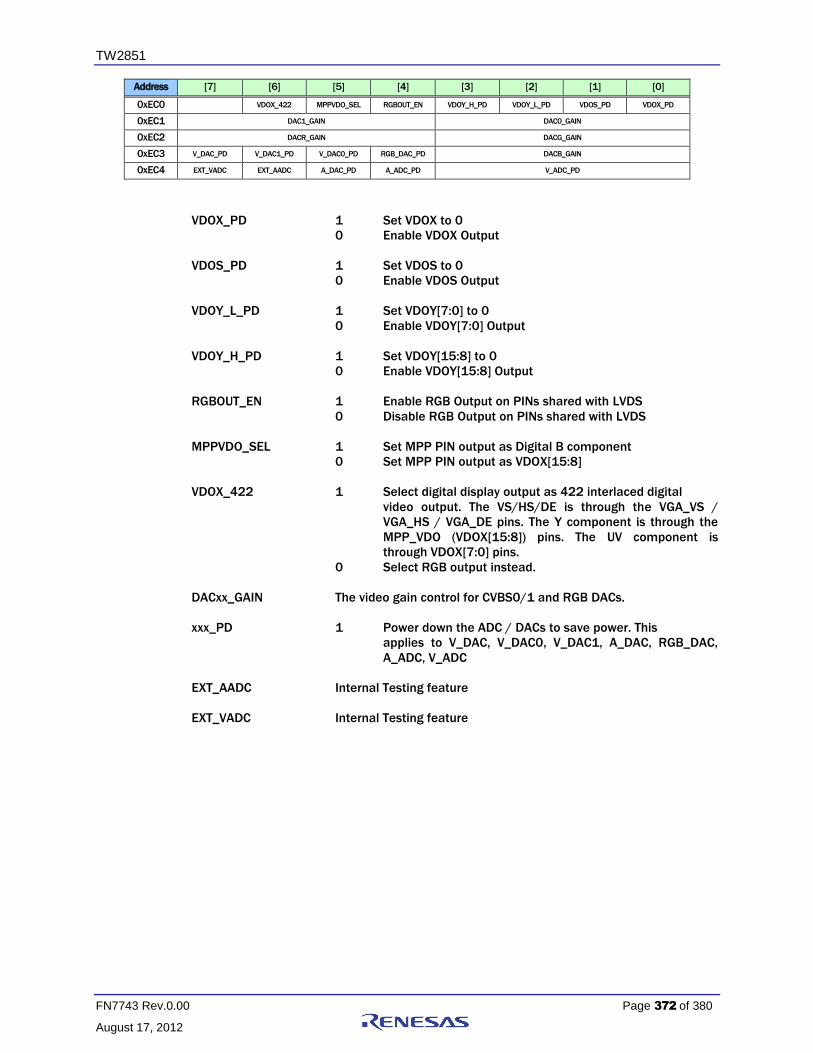
TW2851
FN7743 Rev.0.00 Page 372 of 380
August 17, 2012
Address [7] [6] [5] [4] [3] [2] [1] [0]
0xEC0 VDOX_422 MPPVDO_SEL RGBOUT_EN VDOY_H_PD VDOY_L_PD VDOS_PD VDOX_PD
0xEC1 DAC1_GAIN DAC0_GAIN
0xEC2 DACR_GAIN DACG_GAIN
0xEC3 V_DAC_PD V_DAC1_PD V_DAC0_PD RGB_DAC_PD DACB_GAIN
0xEC4 EXT_VADC EXT_AADC A_DAC_PD A_ADC_PD V_ADC_PD
VDOX_PD 1 Set VDOX to 0
0 Enable VDOX Output
VDOS_PD 1 Set VDOS to 0
0 Enable VDOS Output
VDOY_L_PD 1 Set VDOY[7:0] to 0
0 Enable VDOY[7:0] Output
VDOY_H_PD 1 Set VDOY[15:8] to 0
0 Enable VDOY[15:8] Output
RGBOUT_EN 1 Enable RGB Output on PINs shared with LVDS
0 Disable RGB Output on PINs shared with LVDS
MPPVDO_SEL 1 Set MPP PIN output as Digital B component
0 Set MPP PIN output as VDOX[15:8]
VDOX_422 1 Select digital display output as 422 interlaced digital
video output. The VS/HS/DE is through the VGA_VS /
VGA_HS / VGA_DE pins. The Y component is through the
MPP_VDO (VDOX[15:8]) pins. The UV component is
through VDOX[7:0] pins.
0 Select RGB output instead.
DACxx_GAIN The video gain control for CVBS0/1 and RGB DACs.
xxx_PD 1 Power down the ADC / DACs to save power. This
applies to V_DAC, V_DAC0, V_DAC1, A_DAC, RGB_DAC,
A_ADC, V_ADC
EXT_AADC Internal Testing feature
EXT_VADC Internal Testing feature

TW2851
FN7743 Rev.0.00 Page 373 of 380
August 17, 2012
Address [7] [6] [5] [4] [3] [2] [1] [0]
0xEC5 VGA_CLK_POL VGA_DAC_CLK_POL DAC0_CLK_POL DAC1_CLK_POL
0xEC8 0 0 A_DAC_BIAS_SEL
VGA_CLK_POL Change the VGA output clock polarity
VGA_DAC_CLK_POL Change the polarity of the clock used by the VGA DACs
DAC0_CLK_POL Change the polarity of the clock used by CVBS0 DAC
DAC1_CLK_POL Change the polarity of the clock used by CVBS1 DAC
A_DAC_BIAS_SEL Bias Selection
0 Use AVDD33 as the reference voltage
1 Use bandgap voltage as the reference
AC Timing TABLE 22. CASCADE CLOCK TIMING PARAMETERS
PARAMETER SYMBOL MIN TYP MAX UNITS
Setup from VDIX to CLKIX 1a 3 ns
Hold from CLKIX to VDIX 1b 3 ns
Setup from VDIY to CLKIY 2a 3 ns
Hold from CLKIY to VDIY 2b 3 ns
Setup from VDIS to CLKIS 3a 3 ns
Hold from CLKIS to VDIS 3b 3 ns
TW2851
FN7743 Rev.0.00 Page 374 of 380
August 17, 2012
FIGURE 59. CASCADE INTERFACE TIMING DIAGRAM
TABLE 23. PLAYBACK INTERFACE TIMING PARAMETERS
PARAMETER SYMBOL MIN TYP MAX UNITS
Setup from PB0_DIN to PB0_CLK 4a 3 ns
Hold from PB0_CLK to PB0_DIN 4b 3 ns
Setup from PB1_DIN to PB1_CLK 5a 3 ns
Hold from PB1_CLK to PB1_DIN 5b 3 ns
Setup from PB2/3_DIN to PB2/3_CLK 6a 3 ns
Hold from PB2/3_CLK to PB2/3_DIN 6b 3 ns
1a 1b
CLKIX
VDIX
(A) CLKIX Input Timing
2a 2b
CLKIY
VDIY
(B) CLKIY Input Timing
3a 3b
CLKIS
VDIS
(C) CLKIS Input Timing
TW2851
FN7743 Rev.0.00 Page 375 of 380
August 17, 2012
FIGURE 60. PLAYBACK INTERFACE TIMING DIAGRAM
4a 4b
PB0_CLK
PB0_DIN
(A) PB0_CLK(108MHz Max.) Input Timing
5a 5b
PB1_CLK
PB1_DIN
(B) PB1_CLK(54MHz Max.) Input Timing
6a 6b
PB2_CLK
PB3_CLK
PB2_DIN
PB3_DIN
(C) PB2/3_CLK(27MHz) Input Timing
TW2851
FN7743 Rev.0.00 Page 376 of 380
August 17, 2012
7b
7a
CLKOX
VDOX
(A) CLKOX(108MHz Max.) Input Timing
8b
8a
CLKOY
VDOY
(B) CLKOY(108MHz Max.) Input Timing
9b
9a
CLKOS
VDOS
(C) CLKOS(27MHz) Input Timing
TABLE 24. DIGITAL VIDEO OUTPUT TIMING PARAMETERS
PARAMETER SYMBOL MIN TYP MAX UNITS
Hold from CLKOX to VDOX 7a 2 ns
Delay from CLKOX to VDOX 7b 7.2 ns
Hold from CLKOY to VDOY 8a 2
Delay from CLKOY to VDOY 8b 7.2
Hold from CLKOS to VDOS 9a 5
Delay from CLKOS to VDOS 9b 31.8
FIGURE 61. DIGITAL VIDEO OUTPUT TIMING DIAGRAM
Parametric Information
AC/DC Electrical Parameters TABLE 25. CHARACTERISTICS

TW2851
FN7743 Rev.0.00 Page 377 of 380
August 17, 2012
PARAMETER SYMBOL MIN
(NOTE 1) TYP
MAX
(NOTE 1) UNITS
POWER SUPPLY
Power Supply — Digital I/O VVDDO 2.97 3.3 3.63 V
IVDDO 120 mA
PVDDO 396 mW
Power Supply — LVDS I/O, SPLL VLVDDO,
VVDDSPLL 2.97 3.3 3.63 V
ILVDDO,
IVDDSPLL 5 mA
PLVDDO,
PVDDSPLL 16.5 mW
Power Supply — SSTL I/O VVDDPSSTL 2.3 2.5 2.7 V
IVDDPSSTL 130 mA
PVDDPSSTL 325 mW
Power Supply — Analog CVBS A/D VVDDVADC 2.97 3.3 3.63 V
IVDDVADC 60 mA
PVDDVADC 198 mW
Power Supply — Analog CVBS D/A VVDDDVDAC,
VVDDAVDAC 2.97 3.3 3.63 V
IVDDVDAC 80 mA
PVDDVDAC 264 mW
Power Supply — Analog RGB D/A VVDDDRGB,
VVDDARGB 2.97 3.3 3.63 V
IVDDRGB 60 mA
PVDDRGB 198 mW
Power Supply — Audio Decoder A/D, D/A VVDDAADC,
VVDDADAC, 2.97 3.3 3.63 V
IVDDAADC,
IVDDADAC, 20 mA
PVDDAADC,
PVDDADAC, 66 mW
Power Supply — DLL, SSTL Core, Digital
Core, MPLL, PPLL
VVDDDLL,
VVDDSSTL,
VVDDI,
VVDDMPLL,
VVDDPPLL
1.08 1.2 1.32 V
IVDD 320 mA
PVDD 384 mW
Voltage Reference for SSTL PAD VVREFSSTL 1.25 V
IVREFSSTL 2 mA
PVREFSSTL 2.5 mW
Ambient Operating Temperature TA -40 +85 °C
DIGITAL INPUTS
Input High Voltage (TTL) VIH 2.0 3.6 V
Input Low Voltage (TTL) VIL -0.3 0.8 V

TW2851
FN7743 Rev.0.00 Page 378 of 380
August 17, 2012
PARAMETER SYMBOL MIN
(NOTE 1) TYP
MAX
(NOTE 1) UNITS
Input High Current (VIN = VDD ) IIH 10 A
Input Low Current (VIN = VSS) IIL –10 A
Input Capacitance (f =1 MHz, V IN = 2.4 V) C IN 6 pF
DIGITAL OUTPUTS
Output High Voltage (IOH = –4mA) VOH 2.4 VDD33 V
Output Low Voltage (IOL = 4mA) VOL 0.4 V
3-State Current IOZ 10 A
Output Capacitance CO 6 pF
ANALOG INPUT
Analog Pin Input Voltage at VIN1A, VIN1B,
VIN2A, VIN2B, VIN3, VIN3B, VIN4A, VIN4B,
AIN1, AIN2, AIN3, AIN4, AIN5 Input Range
(AC Coupling Required)
Vi 0 1.0 2.0 Vpp
Analog Pin Input Capacitance C A 6 pF
ADCS
ADC Resolution ADCR 10 bits
ADC Integral Non-Linearity AINL 1 LSB
ADC Differential Non-Linearity ADNL 1 LSB
ADC Clock Rate fADC 24 27 30 MHz
HORIZONTAL PLL
Line Frequency (50Hz) fLN 15.625 KHz
Line Frequency (60Hz) fLN 15.734 KHz
Static Deviation fH 6.2 %
SUBCARRIER PLL
Subcarrier Frequency (NTSC-M) fSC 3579545 Hz
Subcarrier Frequency (PAL-BDGHI) fSC 4433619 Hz
Subcarrier Frequency (PAL-M) fSC 3575612 Hz
Subcarrier Frequency (PAL-N) fSC 3582056 Hz
Lock In Range fH 450 Hz
CRYSTAL SPEC
Nominal Frequency (Fundamental) 27 MHz
Deviation 50 ppm
Temperature Range Ta -40 85 oC
Load Capacitance CL 20 pF
Series Resistor RS 80 Ohm NOTE:
1. Compliance to datasheet limits is assured by one or more methods: production test, characterization and/or
design.

TW2851
FN7743 Rev.0.00 Page 379 of 380
August 17, 2012
Package Outline Drawing

TW2851
For additional products, see www.intersil.com/product_tree
Intersil products are manufactured, assembled and tested utilizing ISO9001 quality systems as noted
in the quality certifications found at http://www.intersil.com/en/support/qualandreliability.html
Intersil products are sold by description only. Intersil may modify the circuit design and/or specifications of products at any time without notice,
provided that such modification does not, in Intersil's sole judgment, affect the form, fit or function of the product. Accordingly, the reader is
cautioned to verify that datasheets are current before placing orders. Information furnished by Intersil is believed to be accurate and reliable.
However, no responsibility is assumed by Intersil or its subsidiaries for its use; nor for any infringements of patents or other rights of third parties
which may result from its use. No license is granted by implication or otherwise under any patent or patent rights of Intersil or its subsidiaries.
For information regarding Intersil Corporation and its products, see http://www.intersil.com
FN7743 Rev.0.00 Page 380 of 380
August 17, 2012
Life Support Policy These products are not authorized for use as critical components in life support devices or systems.
Revision History
REVISION DATE CHANGES NOTE
FN7743.0 August 17, 2012 Initial release.
© Copyright Intersil Americas LLC 2012. All Rights Reserved.
All trademarks and registered trademarks are the property of their respective owners.


![MA251 Computer Organization and Architecture [3-0-0-6] · PDF fileMA251 Computer Organization and Architecture [3-0-0-6] Lecture 5: Decoder, Demultiplexer, Encoder, and Multiplexer..](https://static.fdocuments.in/doc/165x107/5ab3de307f8b9aea528eaf52/ma251-computer-organization-and-architecture-3-0-0-6-computer-organization-and.jpg)


