LLLLINEAR AND DIGITAL IC IICC IC - kopykitab.com€¦ · 4.9.2 3-to-8 Line Decoder ... 4.11.1...
16
L L L INEAR INEAR INEAR INEAR AND AND AND AND D D D IGITAL IGITAL IGITAL IGITAL IC IC IC IC S S S ARUN RANA Assistant Professor Department of Electronics & Communication Engineering Doon Valley Institute of Engineering & Technology Karnal, Haryana Vayu Education of India 2/25, Ansari Road, Darya Ganj, New Delhi-110 002 (An ISO 9001:2008 Certified Company)
Transcript of LLLLINEAR AND DIGITAL IC IICC IC - kopykitab.com€¦ · 4.9.2 3-to-8 Line Decoder ... 4.11.1...

LLLLINEARINEARINEARINEAR
ANDANDANDAND
DDDDIGITALIGITALIGITALIGITAL IC IC IC ICSSSS
ARUN RANAAssistant Professor
Department of Electronics & Communication Engineering
Doon Valley Institute of Engineering & Technology
Karnal, Haryana
Vayu Education of India2/25, Ansari Road, Darya Ganj, New Delhi-110 002
(An ISO 9001:2008 Certified Company)
Linear and Digital ICs
Copyright ©VAYU EDUCATION OF INDIA
ISBN: 978-93-83137-98-5
First Edition: 2013
Price: 160/-
All rights reserved. No part of this publication may be reproduced, stored in a retrieval
system, or transmitted, in any form or by any means, electronic, mechanical, photocopying,
recording or otherwise, without the prior permission of the Author and Publisher.
Printed & bound in India
Published by:
(An ISO 9001:2008 Certified Company)
VAYU EDUCATION OF INDIA2/25, Ansari Road, Darya Ganj, New Delhi-110 002
Ph.: 91-11-43526600, 41564445
Fax: 91-11-41564440
E-mail: [email protected]
Web: www.veiindia.com
1. LINEAR IC ..................................................................................... 1-24
1.1 What is an OP-AMP? ...............................................................................11.2 OP-AMP Symbol ......................................................................................21.3 Polarity Conventions .................................................................................21.4 Ideal Operational Amplifier ......................................................................31.5 Virtual Ground and Summing Point .........................................................41.6 Why Vi is Reduced to almost Zero ? ........................................................41.7 OP-AMP Applications ..............................................................................51.8 Linear Amplifier .......................................................................................51.9 Multivibrators (MV) .................................................................................71.10 Uses of Multivibrators ..............................................................................81.11 Astable Multivibrator ................................................................................81.12 Monostable Multivibrator (MMV) ..........................................................111.13 Bistable Multivibrator (BMV) .................................................................131.14 Schmitt Trigger .......................................................................................151.15 Voltage Regulation .................................................................................. 171.16 Zener Diode Shunt Regulator .................................................................181.17 Emmition Regulator ...............................................................................191.18 Controlled Transistor Series Regulator ....................................................201.19 Transistor Shunt Voltage Regulator .........................................................211.20 Transistor Current Regulator ..................................................................221.21 Transistor Blocking Oscillator .................................................................23
Questions .........................................................................................Questions .........................................................................................Questions .........................................................................................Questions ......................................................................................... 24
2. BOOLEAN ALGEBRA ................................................................... 25-78
2.1 INtroduction ..........................................................................................252.2 Decimal Number System .......................................................................262.3 Binary Number System........................................................................... 272.4 Advantage of Binary Numbers ................................................................272.5 Binary To Decimal Conversion ...............................................................282.6 Decimal To Binary Conversion ...............................................................292.7 binary arithmetic ....................................................................................302.8 binary subtraction ................................................................................... 312.9 binary multiplication ...............................................................................322.10 Binary Division .......................................................................................33
CCCCONTENTSONTENTSONTENTSONTENTS

iv Linear and Digital ICs
2.11 octal number system ...............................................................................342.12 Octal to decimal conversion ...................................................................352.13 Decimal to octal conversion ...................................................................352.14 Octal to binary conversion .....................................................................362.15 Binary to octal conversion ......................................................................372.16 Octal arithmetic ......................................................................................372.17 Octal subtraction ....................................................................................382.18 Octal Multiplication ................................................................................392.19 Octal division .........................................................................................392.20 Hexadecimal number system ..................................................................402.21 Hexadecimal to decimal conversion .......................................................412.22 Decimal to hex conversion .....................................................................422.23 Hexadecimal to binary conversion ..........................................................432.24 Binary to hexadecimal conversion ..........................................................442.25 Hexadecimal to octal conversion ............................................................452.26 Octal to hexadecimal conversion ............................................................452.27 Hexadecimal arithmetics ........................................................................462.28 Hexadecimal subtraction ........................................................................472.29 Hexadecimal multiplication ....................................................................482.30 Hexadecimal division .............................................................................492.31 Complements ..........................................................................................502.32 Subtraction with complements................................................................512.33 Subtraction with (r-1)’s complement .......................................................522.34 Signed Binary Numbers ..........................................................................532.35 Addition of signed binary numbers ........................................................542.36 Subtraction of signed binary numbers ....................................................542.37 Basic laws and theorems .........................................................................542.38 Axioms of Boolean Algebra .....................................................................552.39 Laws of Boolean Algebra .........................................................................552.40 Demorgan’s Theorem ..............................................................................592.41 Implementation Of Boolean Expression With Logic Gates ....................602.42 Complement Of A Function ...................................................................612.43 Minterms And Maxterms .......................................................................622.44 Standard Sum Of Product Form.............................................................642.45 Standard Product Of Sum (Pos) Form ....................................................652.46 Conversion Between Canonical Forms ...................................................662.47 logic gates ...............................................................................................682.48 And gate ..................................................................................................682.49 Or gate ....................................................................................................692.50 Not gate or inverter ................................................................................702.51 Universal building blocks (universal gates) ..............................................712.52 Nand gate ...............................................................................................712.53 Nor gate ..................................................................................................722.54 Exclusive-or (XOR) gate .........................................................................73
Contents v
2.55 Exclusive-nor (x-nor) gate .......................................................................742.56 Summary of gates ...................................................................................74
Questions .........................................................................................Questions .........................................................................................Questions .........................................................................................Questions ......................................................................................... 76767676
3. SIMPLIFICATION OF BOOLEAN FUNCTIONS ............................ 79-98
3.1 Introduction ............................................................................................ 793.2 K-map of Two-three And Four Variables .................................................793.3 Representation of truth table on k-map ..................................................803.4 Simplification of boolean functions using k-map ....................................813.5 Other forms of karnaugh maps-(veitch diagram) ....................................853.6 Don’t care conditions ..............................................................................863.7 Five variable k-map ................................................................................873.8 Six variable k-map ..................................................................................893.9 Tabular Method—(Quine-mc Cluskey Method) .....................................903.10 Cyclic Prime Implicant Chart ................................................................953.11 Example of Simplification Of A Function With Don’t Care ...................96
Questions .........................................................................................Questions .........................................................................................Questions .........................................................................................Questions ......................................................................................... 98989898
4. COMBINATIONAL LOGIC CIRCUITS ......................................... 99-133
4.1 Introduction ............................................................................................ 994.2 Adders ....................................................................................................994.3 Half Adder ............................................................................................ 1004.4 full adder ...............................................................................................1014.5 Adder circuits .......................................................................................103
4.5.1 Serial Adder ............................................................................1034.5.2 Parallel Adders .........................................................................103
4.6 subtractors ............................................................................................1064.6.1 Half Subtractor .......................................................................1074.6.2 Full Subtractor ........................................................................1084.6.3 Parallel Subtractor ...................................................................109
4.6.4 Subtrraction using Full Adders .............................................................1094.7 4 bit adder-subtractor ........................................................................... 1104.8 magnitude comparator ..........................................................................1114.9 Decoders ..............................................................................................112
4.9.1 Basic Binary decoder ................................................................1124.9.2 3-to-8 Line Decoder ................................................................. 1134.9.3 4-Line to 16-Line Decoder .......................................................114
4.10 Encoders ...............................................................................................1154.10.1 Octal to Binary Encoder ...........................................................1164.10.2 Decimal-to-BCD encoder..........................................................117
4.11 Multiplexers (Data Selectors) ................................................................1184.11.1 Multiplexer Tree ....................................................................... 1204.11.2 Application of Multiplexers .......................................................121
vi Linear and Digital ICs
4.12 demultiplexers (data distributors) ..........................................................1214.12.1 De-Multiplexer Tree ................................................................. 122
4.13 Read Only memories ............................................................................1234.14 Types of Roms ......................................................................................1264.15 Programmable logic devices ................................................................. 1274.16 Programmable Logic Arrays (PLA) .......................................................1274.17 Programmable array logic (PAL) ...........................................................130
Questions .......................................................................................Questions .......................................................................................Questions .......................................................................................Questions ....................................................................................... 132132132132
5. SEQUENTIAL LOGIC CIRCUITS ............................................... 134-175
5.1 Introduction .......................................................................................... 1345.2 Gate delays and timing diagram............................................................1355.3 1-bit memory unit ................................................................................. 1375.4 Nor gate latch .......................................................................................1385.5 S-R Flip flop ......................................................................................... 1395.6 D-Flip flop ............................................................................................ 1405.7 J-K Flip Flop .........................................................................................1415.8 T-Flip-Flop ............................................................................................ 1425.9 Master-slave Flip-flop .......................................................................... 1435.10 Master-slave J-k Flip-flop ......................................................................1445.11 Edge triggered flip-flops ........................................................................1445.12 Asynchronous Inputs ............................................................................1455.13 Excitation Table ..................................................................................... 1465.14 Conversion of Flip-flops .......................................................................1475.15 Conversion of S-R Flip-Flop to A J-K Flip-Flop ...................................1485.16 Conversion of S-r Flip-flop To A J-k Flip-flop ......................................1495.17 conversion from S-R flip-flop to D flip-flop ..........................................1505.18 Conversion From J-k Flip-flop To D Flip-flop ......................................1505.19 Conversion From D Flip-flop To J-k Flip-flop ......................................1505.20 Analysis of Clocked Sequential Circuits ...............................................1515.21 Analysis With J-k And Other Flip-flops ................................................1535.22 State Assignment ...................................................................................1555.23 Registers ...............................................................................................1565.24 4 Bit Shift Register ............................................................................... 1565.25 Shift Registers ....................................................................................... 1565.26 shift right register .................................................................................1595.27 Counters ...............................................................................................1635.28 Asynchronous (Ripple Or Serial) Counter ............................................1645.29 Synchronous (Parallel) Counter .............................................................1665.30 Asynchronous Sequential Circuits ........................................................1685.31 Analysis Of Asynchronous Sequential Circuits .....................................1705.32 Flowtable ..............................................................................................1725.33 Race conditions and cycles ...................................................................173
Contents vii
6. D/A AND A/D ........................................................................... 176-203
6.1 D/A and A/D conversion .....................................................................1766.2 Variable Resistor Network ....................................................................176
6.2.1 Binary Weight ..........................................................................1776.3 Binary Ladder .......................................................................................182
6.3.1 Input Resistance .......................................................................1826.3.2 Termination .............................................................................186
6.4 D/A Converter .....................................................................................1896.4.1 Multiplexer ..............................................................................190
6.5 D/A Accuracy and Resolution ..............................................................1936.5.1 Resolution ................................................................................194
6.6 A/D Converter-Simultaneous Conversion ............................................ 1956.7 AID Converter-Counter Method..........................................................198
6.7.1 Control ....................................................................................2006.8 Advanced A/D Techniques ...................................................................203
6.8.1 Continuous ..............................................................................203
Questions .......................................................................................Questions .......................................................................................Questions .......................................................................................Questions ....................................................................................... 203203203203
7. MEMORIES ............................................................................. 204-226
7.1 Introduction ..........................................................................................2047.2 Classification Of Memories .................................................................205
7.2.1 Registers, Main Memory and Secondary Memory ......................2057.2.2 Sequential Access Memory and Random Access Memory ............2057.2.3 Static and Dynamic Memory ....................................................2057.2.4 Volatile and Non-volatile Memory ............................................2067.2.5 Magnetic and Semiconductor Memory ......................................206
7.3 Basic Memory Operation .....................................................................2067.4 Random Access Memory (Ram) ...........................................................207
7.4.1 Static RAM ............................................................................. 2087.4.2 Dynamic RAM (DRAM) ..........................................................212
7.5 Read Only Memory (Rom) ...................................................................2137.5.1 Types of ROM..........................................................................215
7.6 Programmable Logic Devices (Pld) ......................................................2207.6.1 Programmable Logic Array (PLA) ............................................. 2227.6.2 Programmable Array Logic (PAL) ............................................. 223
7.7 Field Programmable Gate Array (Fpga) ................................................225
Questions .......................................................................................Questions .......................................................................................Questions .......................................................................................Questions ....................................................................................... 226226226226
Index .....................................................................................Index .....................................................................................Index .....................................................................................Index ..................................................................................... 227-228227-228227-228227-228
1.1 WHAT IS AN OP-AMP?
It is a very high-gain, high-rin directly-coupled negative-feedback amplifier which
can amplify signals having frequency ranging from 0 Hz to a little beyond 1 MHz.
They are made with different internal configurations in linear ICs. An OP-AMP is so
named because it was originally designed to perform mathematical operations like
summation, subtraction, multiplication, differentiation and integration etc., in analog
computers. Present day usage is much wider in scope but the popular name OP-AMP
continues.
Typical uses of OP-AMP are : scale changing, analog computer operations, in
instrumentation and control systems and a great variety of phase-shift and oscillator
circuits. The OP-AMP is available in three different packages (i) standard dual-in-line
package (DIP) (ii) TO-5 case and (iii) the flat-pack.
Although an OP-AMP is a complete amplifier, it is so designed that external
components (resistors, capacitors etc.) can be connected to its terminals to change its
external characteristics. Hence, it is relatively easy to tailor this amplifier to fit a
particular application and it is, in fact, due to this versatility that OP-AMPs have
become so popular in industry.
An OP-AMP IC may contain two dozen transistors, a dozen resistors and one or
two capacitors. Example of OP-AMPs
1. �A 709-is a high-gain operational amplifier constructed on a single silicon
chip using planar epitaxial process.
It is intended for use in dc servo systems, high-impedance analog computers
and in low-level instrumentation applications.
It is manufactured by Semiconductors Limited, Pune.
2. [LM 108 - LM 208]- Manufactured by Semiconductors Ltd., Mumbai.
3. CA 741 CT and CA 741 T-these are high-gain operational amplifiers which
are intended for use as (i) comparator, (ii) integrator, (iii) differentiator,
(iv) summer, (v) dc amplifier, (vi) multi vibrator, and (vii) band pass filter.
Manufactured by Bharat Electronics Ltd. (BEL), Bangalore.
LLLLINEARINEARINEARINEAR IC IC IC IC
Chapter-1
2 Linear and Digital ICs
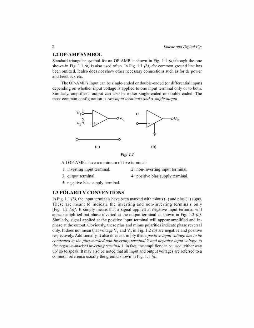
1.2 OP-AMP SYMBOL
Standard triangular symbol for an OP-AMP is shown in Fig. 1.1 (a) though the one
shown in Fig. 1.1 (b) is also used often. In Fig. 1.1 (b), the common ground line has
been omitted. It also does not show other necessary connections such as for dc power
and feedback etc.
The OP-AMP’s input can be single-ended or double-ended (or differential input)
depending on whether input voltage is applied to one input terminal only or to both.
Similarly, amplifier’s output can also be either single-ended or double-ended. The
most common configuration is two input terminals and a single output.
Fig. 1.1
All OP-AMPs have a minimum of five terminals
1. inverting input terminal, 2. non-inverting input terminal,
3. output terminal, 4. positive bias supply terminal,
5. negative bias supply terminal.
1.3 POLARITY CONVENTIONS
In Fig. 1.1 (b), the input terminals have been marked with minus (–) and plus (+) signs.
These are meant to indicate the inverting and non-inverting terminals only
[Fig. 1.2 (a)]. It simply means that a signal applied at negative input terminal will
appear amplified but phase inverted at the output terminal as shown in Fig. 1.2 (b).
Similarly, signal applied at the positive input terminal will appear amplified and in-
phase at the output. Obviously, these plus and minus polarities indicate phase reversal
only. It does not mean that voltage V1 and V2 in Fig. 1.2 (a) are negative and positive
respectively. Additionally, it also does not imply that a positive input voltage has to be
connected to the plus-marked non-inverting terminal 2 and negative input voltage to
the negative-marked inverting terminal 1. In fact, the amplifier can be used ‘either way
up’ so to speak. It may also be noted that all input and output voltages are referred to a
common reference usually the ground shown in Fig. 1.1 (a).
Linear IC 3
Fig. 1.2
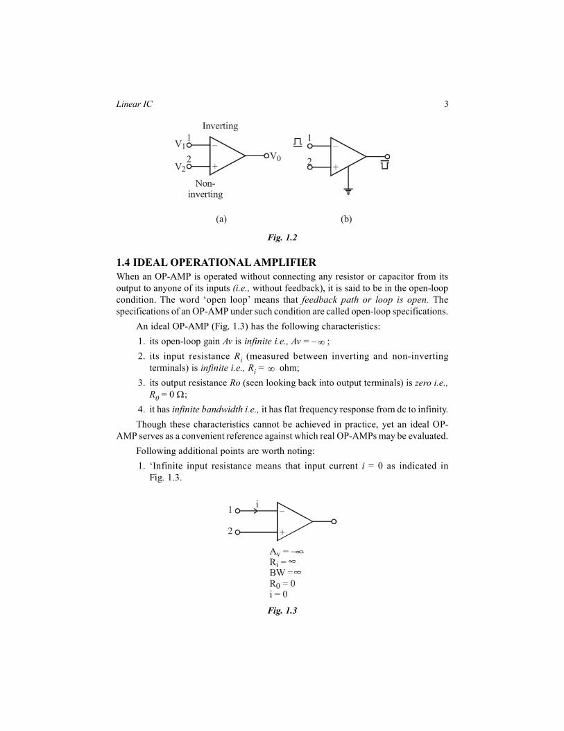
1.4 IDEAL OPERATIONAL AMPLIFIER
When an OP-AMP is operated without connecting any resistor or capacitor from its
output to anyone of its inputs (i.e., without feedback), it is said to be in the open-loop
condition. The word ‘open loop’ means that feedback path or loop is open. The
specifications of an OP-AMP under such condition are called open-loop specifications.
An ideal OP-AMP (Fig. 1.3) has the following characteristics:
1. its open-loop gain Av is infinite i.e., Av = –� ;
2. its input resistance Ri
(measured between inverting and non-inverting
terminals) is infinite i.e., Ri = � ohm;
3. its output resistance Ro (seen looking back into output terminals) is zero i.e.,
R0 = 0 �;
4. it has infinite bandwidth i.e., it has flat frequency response from dc to infinity.
Though these characteristics cannot be achieved in practice, yet an ideal OP-
AMP serves as a convenient reference against which real OP-AMPs may be evaluated.
Following additional points are worth noting:
1. ‘Infinite input resistance means that input current i = 0 as indicated in
Fig. 1.3.
Fig. 1.3

4 Linear and Digital ICs
It means that an ideal OP-AMP is a voltage-controlled device.
2. R0 = 0 means that v0 is not dependent on the load resistance connected across
the output.
3. Though for an ideal OP-AMP Av = � , for an actual one, it is extremely high
i.e., about 106. However, it does not mean that 1 V signal will be amplified to
106 V at the output. Actually, the maximum value of va is limited by the bias
supply voltage, typically + 15 Y. With Av = 106 and V0 = 15 V2 the maximum
value of input voltage is limited to 15/106 = 15 �V. Though 1 V cannot become
1 million volt in the OP-AMP, 1 �V can certainly become 1 V.
1.5 VIRTUAL GROUND AND SUMMING POINT
In Fig. 1.4 is shown an OP-AMP which employs negative feedback with the help of
resistor Rf which feeds a portion of the output to the input.
Since input and feedback currents are algebraically added at point A, it is called
the summing point.
The concept of virtual ground arises from the fact that input voltage Vi at the
inverting terminal of the OP-AMP is forced to such a small 2 value that, for all practical
purposes, it may be assumed to be zero. Hence, point A is essentially at ground voltage
and is referred to as virtual ground. Obviously, it is not the actual ground, which, as
seen from Fig. 1.4, is situated below.
Fig. 1.4
1.6 WHY Vi IS REDUCED TO ALMOST ZERO ?
When vi is applied, point A attains some positive potential and at the same time
Va is brought into existence. Due to negative feedback, some fraction of the
output voltage is fed back to point A antiphase with the voltage already existing there
(due to v1).
The algebraic sum of the two voltages is almost zero so that Vi = 0. Obviously, Vi
will become exactly zero when negative feedback voltage at A is exactly equal to
the positive voltage produced by V1 at A.
Linear IC 5
Another point worth considering is that there exists a virtual short between the
two terminals of the OP-AMP because Vi = 0. It is virtual because no current flows
(remember i = 0) despite ‘the existence of this short.
1.7 OP-AMP APPLICATIONS
We will consider the following applications:
1. as scaler or linear (i.e., small-signal) constant-gain amplifier; both inverting
and non-inverting,
2. as unity follower, 3. Adder or Summer,
4. Subttactor, 5. Integrator,
6. Differentiator, 7. Comparator.
Now, we will discuss the above circuits one by one assuming an ideal OP-AMP.
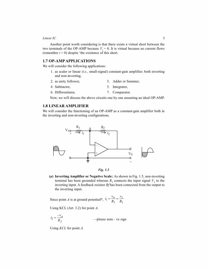
1.8 LINEAR AMPLIFIER
We will consider the functioning of an OP-AMP as a constant-gain amplifier both in
the inverting and non-inverting configurations.
Fig. 1.5
(a) Inverting Amplifier or Negative Scale: As shown in Fig. 1.5, non-inverting
terminal has been grounded whereas R1 connects the input signal V1 to the
inverting input. A feedback resistor Rf has been connected from the output to
the inverting input.
Since point A is at ground potential*, � � 11
1 1
nv vi
R R
Using KCL (Art. 3.2) for point A,
��2
a
f
vi
R —please note - ve sign
Using KCL for point A.
6 Linear and Digital ICs
� � � � � � � �0 0 01 11 2
1 1 1 1
0 or 0 or orf
f f
Rv v vv vi i
R R R R v R
� � � � � � �01
or Also,f
v v in
RA A K v Kv
R
It is seen from above, that closed-loop gain of the inverting amplifier depends on
the ratio of the two external resistors R1 and Rf and is independent of the amplifier
parameters.
It is also seen that the OP-AMP works as a negative scaler. It scales the input i.e.,
it multiplies the input by a minus constant factor K.
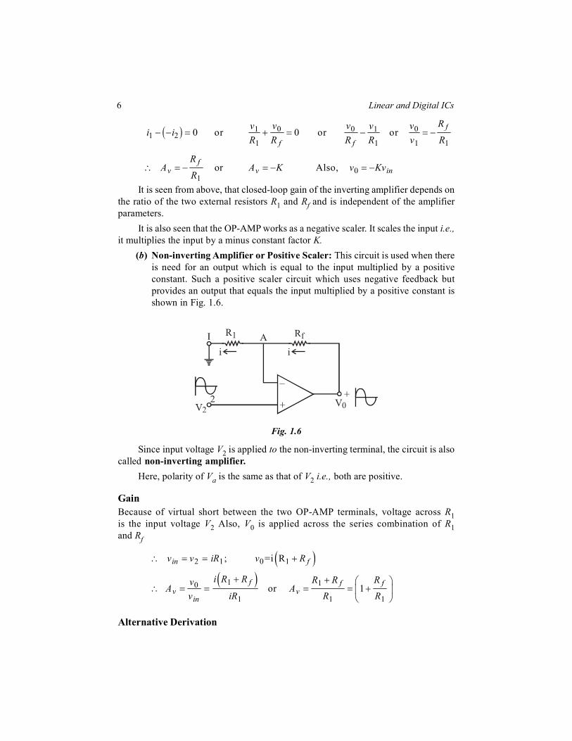
(b) Non-inverting Amplifier or Positive Scaler: This circuit is used when there
is need for an output which is equal to the input multiplied by a positive
constant. Such a positive scaler circuit which uses negative feedback but
provides an output that equals the input multiplied by a positive constant is
shown in Fig. 1.6.
Fig. 1.6
Since input voltage V2 is applied to the non-inverting terminal, the circuit is also
called non-inverting amplifier.
Here, polarity of Va is the same as that of V2 i.e., both are positive.
Gain
Because of virtual short between the two OP-AMP terminals, voltage across R1
is the input voltage V2 Also, V0 is applied across the series combination of R1
and Rf
� � � �
� � � � � � � � � �
�
2 1 0 1
1 10
1 1 1
; =i R
or 1
in f
f f fv v
in
v v iR v R
i R R R R RvA A
v iR R R
Alternative Derivation
Linear IC 7
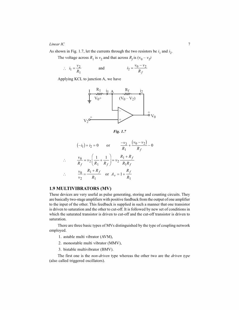
As shown in Fig. 1.7, let the currents through the two resistors be i1 and i2.
The voltage across R1 is v2 and that across Rf is (v0 – v2)
� � 21
1
vi
Rand
�� 0 2
2f
v vi
R
Applying KCL to junction A, we have
Fig. 1.7
��� � � � �
� �� � � � �
�
�� � � �
0 221 2
1
102 2
1 1
10
2 1 1
0 or 0
1 1
or 1
f
f
f f f
f fv
v vvi i
R R
R Rvv v
R R R R R
R R RvA
v R R
1.9 MULTIVIBRATORS (MV)
These devices are very useful as pulse generating, storing and counting circuits. They
are basically two-stage amplifiers with positive feedback from the output of one amplifier
to the input of the other. This feedback is supplied in such a manner that one transistor
is driven to saturation and the other to cut-off. It is followed by new set of conditions in
which the saturated transistor is driven to cut-off and the cut-off transistor is driven to
saturation.
There are three basic types of MVs distinguished by the type of coupling network
employed.
1. astable multi vibrator (AVM),
2. monostable multi vibrator (MMV),
3. bistable multivibrator (BMV).
The first one is the non-driven type whereas the other two are the driven type
(also called triggered oscillators).

8 Linear and Digital ICs
l. Astable Multivibrator (AMV): It is also called free-running relaxation
oscillator. It has no stable state but only two quasistable (half-stable) states
between which it keeps oscillating continuously of its own accord without
any external excitation.
In this circuit, neither of the two transistors reaches a stable state. When one is
ON, the other is OFF and they continuously switch back and forth at a rate depending
on the RC time constant in the circuit. Hence, it oscillates and produces pulses of
certain mark-to-space ratio. Moreover, two outputs (1800 out of phase with each other)
are available.
It has two energy-storing elements i.e. two capacitors.
2. Monostable Multivibrator (MMV): It is also called a single-shot or single
swing or a one-shot multi vibrator. Other names are: delay multivibrator and
univibrator. It has
(i) one absolutely stable (stand-by) state and
(ii) one quasi-stable state.
It can be switched to the quasi-stable state by an external trigger pulse but it
returns to the stable condition after a time delay determined by the value of circuit
components. It supplies a single output pulse of a desired duration for every input
trigger pulse.
It has one energy-storing element i.e., one-capacitor.
3. Bistable Multivibrator (BMV): It is also called Eccles-Jordan or flip-flop
multi vibrator. It has two absolutely stable states. It can remain in either of
these two states unless an external trigger pulse switches it from one state to
the other. Obviously, it does not oscillate. It has no energy storage element.
Detailed discrete circuits for the above MVs are discussed below after listing
their uses.
1.10 USES OF MULTIVIBRATORS
Some of their uses are:
1. as frequency dividers,
2. as sawtooth generators,
3. as square wave and pulse generators,
4. as a standard frequency source when synchronized by an external crystal
oscillator,
5. for many specialised uses in radar and TV circuits,
6. as memory elements in computers
1.11 ASTABLE MULTIVIBRATOR
Fig. 1.8 shows the circuit of a symmetrical collector-coupled AMV using two similar

Linear and Digital ICs By Aruna Rana
Publisher : Vayu Education ISBN : 9789383137985 Author : Aruna Rana
Type the URL : http://www.kopykitab.com/product/3210
Get this eBook