Layer-by-layer assembly of two-dimensional materials into ... · materials into wafer-scale...
5
00 MONTH 2017 | VOL 000 | NATURE | 1 LETTER doi:10.1038/nature23905 Layer-by-layer assembly of two-dimensional materials into wafer-scale heterostructures Kibum Kang 1,2,3 *, Kan-Heng Lee 4,5 *, Yimo Han 4 , Hui Gao 1,2 , Saien Xie 4,5 , David A. Muller 4,6 & Jiwoong Park 1,2,3,5,6 High-performance semiconductor films with vertical compositions that are designed to atomic-scale precision provide the foundation for modern integrated circuitry and novel materials discovery 1–3 . One approach to realizing such films is sequential layer-by-layer assembly, whereby atomically thin two-dimensional building blocks are vertically stacked, and held together by van der Waals interactions 4–6 . With this approach, graphene and transition-metal dichalcogenides—which represent one- and three-atom-thick two- dimensional building blocks, respectively—have been used to realize previously inaccessible heterostructures with interesting physical properties 7–11 . However, no large-scale assembly method exists at present that maintains the intrinsic properties of these two- dimensional building blocks while producing pristine interlayer interfaces 12–15 , thus limiting the layer-by-layer assembly method to small-scale proof-of-concept demonstrations. Here we report the generation of wafer-scale semiconductor films with a very high level of spatial uniformity and pristine interfaces. The vertical composition and properties of these films are designed at the atomic scale using layer-by-layer assembly of two-dimensional building blocks under vacuum. We fabricate several large-scale, high-quality heterostructure films and devices, including superlattice films with vertical compositions designed layer-by-layer, batch-fabricated tunnel device arrays with resistances that can be tuned over four orders of magnitude, band-engineered heterostructure tunnel diodes, and millimetre-scale ultrathin membranes and windows. The stacked films are detachable, suspendable and compatible with water or plastic surfaces, which will enable their integration with advanced optical and mechanical systems. In Fig. 1a, b we show a representative high-quality semiconductor heterostructure film generated using a programmed vacuum stack (PVS) process (explained in Fig. 2). The film is assembled by vertically stacking nine layers of individual wafer-scale, monolayer, transition-metal dichalcogenide (TMD) films, alternating between MoS 2 and WS 2 (see schematic in Fig. 1a). The scanning transmis- sion electron microscopy (STEM) data shown in Fig. 1b confirm the vertically stacked design, and reveal a composition with atomic-scale precision and clean interfaces. First, five dark layers and four bright layers are clearly visible in the cross-sectional annular dark field (ADF) STEM image of the film (Fig. 1b, left), which correspond to the five monolayers of MoS 2 and four monolayers of WS 2 , respectively. The chemical composition of each layer is confirmed by electron energy loss spectroscopy (EELS; Fig. 1b, right), which reveals Mo peaks for only the MoS 2 layers, but a uniform S signal everywhere within the film. Second, all nine individual layers appear uniform and continuous, and run straight and parallel to each other. The interfaces between adjacent lay- ers remain clean and free of bubbles or wrinkles, with a constant inter- layer distance of 0.64 nm, which is consistent with the value expected for MoS 2 /WS 2 with a non-zero interlayer rotation angle 16 . Third, the EELS data further show a very low signal for carbon (Fig. 1b, red curve) within the film, near the detection limit of our instrument. Additional STEM images and EELS spectra of more heterostructure films are shown in Fig. 2e and Supplementary Figs 1 and 2. In Fig. 1c we present another high-quality large-scale semiconductor film, assembled with seven layers of MoS 2 , which is completely separated from the substrate and suspended over a 1 mm × 1 mm hole in the middle of a transmis- sion electron microscope (TEM) chip (see Supplementary Methods and Supplementary Fig. 3). The freestanding film is thinner than 5 nm, and has one of the highest aspect ratios (length-to-thickness ratio of about 0.2 × 10 6 ) ever reported for freestanding semiconductor films 17–19 , indicating that it has excellent structural quality and mechanical strength. Altogether, the data shown in Fig. 1 demonstrate that we have successfully produced high-quality, detachable semiconductor films with atomic-scale programmability and pristine interfaces. Figure 2a schematically illustrates the PVS process (see Supplementary Notes for details): (I) wafer-scale, two-dimensional building blocks (TMD monolayers) are synthesized individually 20 ; (II) the initial layer L0, spin-coated with an adhesive polymer film, is mechanically peeled from the growth substrate (SiO 2 /Si) using a thermal release tape (TRT); (III) L0/TRT is then stacked and pressed on top of the next layer (L1; on the growth substrate) in a vacuum chamber, forming an air-free interface between L0 and L1; (IV) L1/ L0/TRT is peeled off the substrate, and then the vacuum stack (III) and peel (IV) steps are repeated until the film has the desired number of layers N L ; and (V) the N L -layer film is released from the TRT onto a target substrate, in either supported or suspended form. The PVS process was designed to provide two key advantages over existing methods: the wafer-scale fabrication and the generation of pristine interlayer interfaces. For the former, a metal–organic chemical vapour deposition process 20 is used to grow homogeneous wafer-scale semiconductor monolayers as the building blocks (MoS 2 , MoSe 2 and WS 2 ). For the latter, we optimize the synthesis to generate surface properties that enable these building blocks to be cleanly peeled off the growth substrates without the use of any etchants or solvents (see Supplementary Notes and Supplementary Video 1). These building blocks are then assembled under vacuum using a customized apparatus for wafer-scale vacuum stacking (Supplementary Fig. 13). As we show below, this vacuum stacking greatly improves the interface quality and flatness of the films, minimizing the amount of amorphous carbon or trapped air at the interfaces. Moreover, the PVS process can be used with any arbitrary two-dimensional building block as long as the adhesion to the stacked film is stronger than that to the growth substrate, making it a general approach for producing large-scale, vertically stacked films with pristine interfaces. These key advantages are realized in our films, as confirmed by the following experiments. We use multiple characterization techniques in combination (see Supplementary Table 1 for a summary), each of which covers a different and overlapping length scale, from sub-nanometre to centimetre scale. First, we confirm that our stacked films are spatially 1 Department of Chemistry and Chemical Biology, Cornell University, Ithaca, New York 14853, USA. 2 Department of Chemistry, University of Chicago, Chicago, Illinois 60637, USA. 3 James Franck Institute, University of Chicago, Chicago, Illinois 60637, USA. 4 School of Applied and Engineering Physics, Cornell University, Ithaca, New York 14853, USA. 5 Institute for Molecular Engineering, University of Chicago, Chicago, Illinois 60637, USA. 6 Kavli Institute at Cornell for Nanoscale Science, Cornell University, Ithaca, New York 14853, USA. *These authors contributed equally to this work. © 2017 Macmillan Publishers Limited, part of Springer Nature. All rights reserved.
Transcript of Layer-by-layer assembly of two-dimensional materials into ... · materials into wafer-scale...

0 0 M o n t h 2 0 1 7 | V o L 0 0 0 | n A t U R E | 1
LEttERdoi:10.1038/nature23905
Layer-by-layer assembly of two-dimensional materials into wafer-scale heterostructuresKibum Kang1,2,3*, Kan-heng Lee4,5*, Yimo han4, hui Gao1,2, Saien Xie4,5, David A. Muller4,6 & Jiwoong Park1,2,3,5,6
High-performance semiconductor films with vertical compositions that are designed to atomic-scale precision provide the foundation for modern integrated circuitry and novel materials discovery1–3. One approach to realizing such films is sequential layer-by-layer assembly, whereby atomically thin two-dimensional building blocks are vertically stacked, and held together by van der Waals interactions4–6. With this approach, graphene and transition-metal dichalcogenides—which represent one- and three-atom-thick two-dimensional building blocks, respectively—have been used to realize previously inaccessible heterostructures with interesting physical properties7–11. However, no large-scale assembly method exists at present that maintains the intrinsic properties of these two-dimensional building blocks while producing pristine interlayer interfaces12–15, thus limiting the layer-by-layer assembly method to small-scale proof-of-concept demonstrations. Here we report the generation of wafer-scale semiconductor films with a very high level of spatial uniformity and pristine interfaces. The vertical composition and properties of these films are designed at the atomic scale using layer-by-layer assembly of two-dimensional building blocks under vacuum. We fabricate several large-scale, high-quality heterostructure films and devices, including superlattice films with vertical compositions designed layer-by-layer, batch-fabricated tunnel device arrays with resistances that can be tuned over four orders of magnitude, band-engineered heterostructure tunnel diodes, and millimetre-scale ultrathin membranes and windows. The stacked films are detachable, suspendable and compatible with water or plastic surfaces, which will enable their integration with advanced optical and mechanical systems.
In Fig. 1a, b we show a representative high-quality semiconductor heterostructure film generated using a programmed vacuum stack (PVS) process (explained in Fig. 2). The film is assembled by vertically stacking nine layers of individual wafer-scale, monolayer, transition-metal dichalcogenide (TMD) films, alternating between MoS2 and WS2 (see schematic in Fig. 1a). The scanning transmis-sion electron microscopy (STEM) data shown in Fig. 1b confirm the vertically stacked design, and reveal a composition with atomic-scale precision and clean interfaces. First, five dark layers and four bright layers are clearly visible in the cross-sectional annular dark field (ADF) STEM image of the film (Fig. 1b, left), which correspond to the five monolayers of MoS2 and four monolayers of WS2, respectively. The chemical composition of each layer is confirmed by electron energy loss spectroscopy (EELS; Fig. 1b, right), which reveals Mo peaks for only the MoS2 layers, but a uniform S signal everywhere within the film. Second, all nine individual layers appear uniform and continuous, and run straight and parallel to each other. The interfaces between adjacent lay-ers remain clean and free of bubbles or wrinkles, with a constant inter-layer distance of 0.64 nm, which is consistent with the value expected for MoS2/WS2 with a non-zero interlayer rotation angle16. Third, the EELS data further show a very low signal for carbon (Fig. 1b, red curve)
within the film, near the detection limit of our instrument. Additional STEM images and EELS spectra of more heterostructure films are shown in Fig. 2e and Supplementary Figs 1 and 2. In Fig. 1c we present another high-quality large-scale semiconductor film, assembled with seven layers of MoS2, which is completely separated from the substrate and suspended over a 1 mm × 1 mm hole in the middle of a transmis-sion electron microscope (TEM) chip (see Supplementary Methods and Supplementary Fig. 3). The freestanding film is thinner than 5 nm, and has one of the highest aspect ratios (length-to- thickness ratio of about 0.2 × 10⁶) ever reported for freestanding semiconductor films17–19, indicating that it has excellent structural quality and mechanical strength. Altogether, the data shown in Fig. 1 demonstrate that we have successfully produced high-quality, detachable semiconductor films with atomic-scale programmability and pristine interfaces.
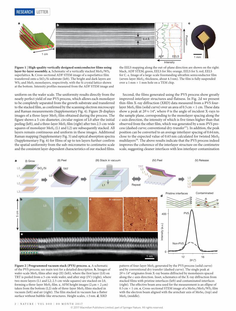
Figure 2a schematically illustrates the PVS process (see Supplementary Notes for details): (I) wafer-scale, two-dimensional building blocks (TMD monolayers) are synthesized individually20; (II) the initial layer L0, spin-coated with an adhesive polymer film, is mechanically peeled from the growth substrate (SiO2/Si) using a thermal release tape (TRT); (III) L0/TRT is then stacked and pressed on top of the next layer (L1; on the growth substrate) in a vacuum chamber, forming an air-free interface between L0 and L1; (IV) L1/L0/TRT is peeled off the substrate, and then the vacuum stack (III) and peel (IV) steps are repeated until the film has the desired number of layers NL; and (V) the NL-layer film is released from the TRT onto a target substrate, in either supported or suspended form.
The PVS process was designed to provide two key advantages over existing methods: the wafer-scale fabrication and the generation of pristine interlayer interfaces. For the former, a metal–organic chemical vapour deposition process20 is used to grow homogeneous wafer-scale semiconductor monolayers as the building blocks (MoS2, MoSe2 and WS2). For the latter, we optimize the synthesis to generate surface properties that enable these building blocks to be cleanly peeled off the growth substrates without the use of any etchants or solvents (see Supplementary Notes and Supplementary Video 1). These building blocks are then assembled under vacuum using a customized apparatus for wafer-scale vacuum stacking (Supplementary Fig. 13). As we show below, this vacuum stacking greatly improves the interface quality and flatness of the films, minimizing the amount of amorphous carbon or trapped air at the interfaces. Moreover, the PVS process can be used with any arbitrary two-dimensional building block as long as the adhesion to the stacked film is stronger than that to the growth substrate, making it a general approach for producing large-scale, vertically stacked films with pristine interfaces.
These key advantages are realized in our films, as confirmed by the following experiments. We use multiple characterization techniques in combination (see Supplementary Table 1 for a summary), each of which covers a different and overlapping length scale, from sub-nanometre to centimetre scale. First, we confirm that our stacked films are spatially
1Department of Chemistry and Chemical Biology, Cornell University, Ithaca, New York 14853, USA. 2Department of Chemistry, University of Chicago, Chicago, Illinois 60637, USA. 3James Franck Institute, University of Chicago, Chicago, Illinois 60637, USA. 4School of Applied and Engineering Physics, Cornell University, Ithaca, New York 14853, USA. 5Institute for Molecular Engineering, University of Chicago, Chicago, Illinois 60637, USA. 6Kavli Institute at Cornell for Nanoscale Science, Cornell University, Ithaca, New York 14853, USA.*These authors contributed equally to this work.
© 2017 Macmillan Publishers Limited, part of Springer Nature. All rights reserved.
2 | n A t U R E | V o L 0 0 0 | 0 0 M o n t h 2 0 1 7
LetterreSeArCH
uniform on the wafer scale. The uniformity results directly from the nearly perfect yield of our PVS process, which allows each monolayer to be completely separated from the growth substrate and transferred to the stacked film, as confirmed by the scanning electron microscopy and Raman measurements (Supplementary Fig. 4). Figure 2b displays images of a three-layer MoS2 film obtained during the process. The figure shows a 5-cm-diameter, circular region of L0 after the initial peeling (left), and a three-layer MoS2 film (right) after two 2.5-cm-wide squares of monolayer MoS2 (L1 and L2) are subsequently stacked. All layers remain continuous and uniform in these images. Additional Raman mapping (Supplementary Fig. 5) and optical absorption spectra (Supplementary Fig. 6) for films of up to ten layers further confirm the spatial uniformity from the sub-micrometre to centimetre scale and the consistent layer-dependent characteristics of our stacked films.
Second, the films generated using the PVS process show greatly improved interlayer structures and flatness. In Fig. 2d we present thin-film X-ray diffraction (XRD) data measured from a PVS four-layer MoS2 film (solid curve) over an area of 0.5 cm × 1 cm. These data show a peak at 2θ ≈ 14°, where θ is the angle of incident X-rays to the sample plane, corresponding to the monolayer spacing along the c-axis direction, the intensity of which is five times higher than that observed from the other film, which was generated by a non-PVS pro-cess (dashed curve; conventional dry-transfer11). In addition, the peak position can be converted to an average interlayer spacing of 0.64 nm, close to the expected value of 0.65 nm calculated for twisted MoS2 multilayers16. The above results indicate that the PVS process indeed improves the coherence of the interlayer structure on the centimetre scale, suggesting cleaner interfaces with less interlayer contamination
a
1 cm
Monolayer M
oS2
Monolayer W
S2
ADF
Mo S C
EELS
Intensity
Position
6.4 Å
b
1 mm
c
Figure 1 | High-quality vertically designed semiconductor films using layer-by-layer assembly. a, Schematic of a vertically stacked MoS2/WS2 superlattice. b, Cross-sectional ADF STEM image of a superlattice film transferred onto a SiO2/Si substrate (left). The bright and dark layers are WS2 and MoS2 monolayers, respectively, with the Si crystal lattice shown at the bottom. Intensity profiles measured from the ADF STEM image and
the EELS mapping along the out-of-plane direction are shown on the right: black, ADF STEM; green, EELS for Mo; orange, EELS for S; red, EELS for C. c, Image of a large-scale freestanding ultrathin semiconductor film (seven-layer MoS2; thickness, about 4.5 nm). The film is fully suspended over a 1 mm × 1 mm hole on a TEM chip.
L0
L1
L2
L3
SiO2/Si
(I) Growa (II) Peel
L0
TRT
Repeat
(III) Stack in vacuum
L1
L0
(IV) Peel
L0L1
L2L3
TRT
L0L1L2L3
(V) Release
In vacuum In airc
L0
TRT
L2
L1L0
5 cm
b
MoSe2
MoS2
WS2
e
Inte
nsity
(a.u
.)
2 (°)12 16
0
400 PVS
Non-PVS
Pristine interfaces Contaminatedd
1 nm
Figure 2 | Programmed vacuum stack (PVS) process. a, A schematic of the PVS process; see main text for a detailed description. b, Images of wafer-scale MoS2 films after step (II) (left), where the first layer (L0) on TRT is peeled from a 5-cm-wide wafer, and after step (IV) (right), where two more layers (L1 and L2; 2.5-cm-wide squares) are stacked on L0, forming a three-layer MoS2 film. c, AFM height images (2 mm × 2 mm) taken from the bottom (L2) side of three-layer MoS2 films stacked in vacuum (left) and air (right). The film stacked in vacuum has a flatter surface without bubble-like structures. Height scales, ± 5 nm. d, XRD
pattern of four-layer MoS2 generated by the PVS process (solid curve) and by conventional dry transfer (dashed curve). The single peak at 2θ ≈ 14° originates from X-ray beams diffracted by monolayers spaced along the c-axis direction. Inset, schematics of the X-ray diffraction from stacked films with pristine interfaces (left) and contaminated interfaces (right). The effective beam area used for the measurement is an ellipse of 0.5 cm × 1 cm. e, Cross-sectional STEM image of a MoSe2/MoS2/WS2 film with the electron beam aligned with the armchair axis of MoSe2 (top) and MoS2 (middle).
© 2017 Macmillan Publishers Limited, part of Springer Nature. All rights reserved.

0 0 M o n t h 2 0 1 7 | V o L 0 0 0 | n A t U R E | 3
Letter reSeArCH
in the films. Dark-field optical microscopy (Supplementary Fig. 7) also shows that the number of scatterers is reduced by 98% over an area of 5 mm × 5 mm in PVS films, confirming the substantial improvement in film flatness achieved by using the PVS process. Furthermore, Fig. 2c shows atomic force microscopy (AFM) images (measured on the bottom side of L2) of two MoS2 films (NL = 3), preparation steps of which are identical except for the stacking environment: one is stacked in vacuum (left) and the other in air (right). The film stacked in vacuum (which has a roughness of about 270 pm) is much smoother than the one stacked in air (roughness of about 700 pm). In addition, the vacuum-stacked film is free of bubble-like features, which are clearly visible in the film stacked in air and are similar to the features reported previously14,15,21. Additional AFM images (Supplementary Fig. 8) show similar improvements for areas of up to 50 m m × 50 m m. The high- quality interfaces in our stacked films also result in strong and uniform interlayer coupling, as suggested by photoluminescence spectroscopy and imaging studies (Supplementary Figs 9 and 10).
Finally, our stacked films can be generated using various two- dimensional building blocks without the constraints of lattice match or alignment. In Fig. 2e we show a cross-sectional STEM image of a MoSe2/MoS2/WS2 film, in which the armchair axes of the MoSe2 (top) and MoS2 (middle) layers are parallel to the electron beam, whereas that of WS2 is not. This image shows that the vertical stacking is successful even in the presence of lattice mismatch (the lattice constant of MoSe2 is larger than that of MoS2 by about 4.2%)22 or interlayer rotation (between MoS2 and WS2).
Our PVS process enables the generation of a large number of distinct, vertically stacked semiconductor films with only a small set of two- dimensional building blocks. For example, with n kinds of two- dimensional building blocks, we can construct nNL distinct films by stacking NL layers. Here, the n different building blocks can be grown individually without considering the specific stacking sequence, making the programming process simple and straightforward. Moreover, these stacked films should enable batch-fabrication of electronic and optoelectronic devices because the PVS process generates homogeneous structures and properties over large areas.
In Fig. 3, we demonstrate above concept by generating a series of distinct stacked films and heterostructures that have a large number of stacked interfaces, all assembled with two representative TMD monolayers (MoS2 and WS2). To study their electrical properties, we fabricate large arrays of metal/stacked-film/metal vertical tunnel devices (Fig. 3a, b; Supplementary Methods). We choose gold as the electrode metal, yielding the tunnel band diagram illustrated schemati-cally in Fig. 3c. Using the tunnel device geometry, we can investigate the uniformity and high quality of PVS films accurately over large areas, because tunnelling is exponentially sensitive to the barrier properties, including the thickness, band structure, doping and defects.
In Fig. 3d we show the representative current density versus bias (J–V) curves measured from NL-layer MoS2 films (NL = 3, 5, 7). All three J–V curves show similar non-Ohmic behaviour, with the current increasing superlinearly with increasing bias. In addition, the magnitude of J strongly depends on NL, decreasing by a factor of
a
c
B
NL-layer TMDAuAu
b
MoS2 WS2 WS2/MoS2–200
0
200
–0.2 0 0.2
V (V)
V (V) V (V)
d
–0.02 0 0.02–0.04
0
0.04
f
V < 0
V ≈ 0
V > 0
–1 0 1
–2
0
2
e
g
3 mm
NL
3 5 74 6
1010
108
106
104
NL = 3NL = 5NL = 7
×102
×104
×102
×103~100 MΩ μm2
<1 MΩ μm2MoS2WS2WS2/MoS2
ExperimentTheory
0
4
2
107 108 109
107 108 109
J (μ
A μ
m–2
)
J (μ
A μ
m–2
)
J (μ
A μ
m–2
)
~10,000 MΩ μm2
R0A
(Ω μ
m2 )
R0A
R0A
Cou
nts
Figure 3 | Tuning electrical conductance of stacked semiconductor films using the number of layers or vertical composition. a, Schematic of our device geometry (see Supplementary Methods for the fabrication process), in which a stacked film is sandwiched between top and bottom electrodes. b, Schematics of devices with different film compositions (top) and their corresponding band profiles (bottom). c, Schematic of the general band profile of our tunnel devices in the zero-bias regime. φB is the barrier height, and e is the electron that tunnels through the barrier. d, J–V characteristics measured from three Au/NL-layer MoS2/Au devices with NL = 3, 5 and 7. The curves for NL = 5 are multiplied by 102 and for NL = 7 by 104. e, Zero-bias tunnel resistance–area product measured as a function of NL (left). Each data point is an average from ten devices; the error bars show the standard deviation. The dashed line is calculated using a tunnel model with a single fitting parameter, φB = 0.5 eV. An optical image of an
array of 24 tunnel devices made with seven-layer MoS2 over an area of 2 mm × 3 mm is shown top right. A spatial map of the tunnel resistance of the 24 devices is shown at bottom right; the corresponding histogram is shown in the inset of the left panel. f, J–V curves near zero bias measured from MoS2, WS2 and WS2/MoS2 devices, all with NL = 6. The curves for WS2/MoS2 and WS2 are multiplied by 102 and 103, respectively. The corresponding tunnel resistance is shown for each J–V curve. g, J–V curve of the heterostructure WS2/MoS2 device in the large bias regime, where the WS2 side is grounded (left), showing diode behaviour with the forward bias current about 10 times larger than the reverse bias current at 1.4 V. The corresponding band diagrams under large reverse bias (V < 0), zero-bias (V ≈ 0) and large forward bias (V > 0) are shown on the right, demonstrating different effective electron tunnelling lengths. Arrows indicate the direction of electron tunnelling.
© 2017 Macmillan Publishers Limited, part of Springer Nature. All rights reserved.

4 | n A t U R E | V o L 0 0 0 | 0 0 M o n t h 2 0 1 7
LetterreSeArCH
approximately ten with each additional layer. Figure 3e (left) displays the average zero-bias resistance–area product (R0A; average from ten devices) as a function of NL, which confirms the exponential dependence on NL. This exponential dependence and the superlinear J–V curves strongly suggest that the main transport mechanism in our devices is electron tunnelling, as shown schematically in Fig. 3c—the same mechanism that has been observed for similar devices made with exfoliated hexagonal boron nitride flakes23. Furthermore, our experi-mental data quantitatively match the theoretical zero-bias resistance, which is calculated on the basis of a tunnel model24 using the barrier height φB as the single fitting parameter (Fig. 3e dashed line, plotted for φB = 0.5 eV).
The agreement between our experimental data and the theoretical model indicates that our MoS2 films have a well-controlled number of layers and band energy (that is, doping level), which are uniform across the entire film, and are without structural inhomogeneities (such as cracks, wrinkles or trapped impurities) that would strongly affect the tunnel current. This result is supported by the spatial map of R0A values measured from an array of 24 tunnel devices with seven-layer MoS2 over an area of 2 mm × 3 mm (Fig. 3e, right). This map shows a 100% (that is, 24 out of 24 devices) device yield with a uniform tunnel resistance. A histogram of the tunnel resistance of these measurements (Fig. 3e, inset) shows a single narrow peak with a standard deviation that corresponds to a thickness variation of only 0.1 layers (about 70 pm; see Supplementary Notes). For larger NL, the control over NL and the spatial uniformity is demonstrated using capacitance meas-urements (Supplementary Fig. 11). The average capacitance values measured from NL-layer MoS2 capacitors (NL up to 11) closely follow the 1/NL dependence expected from a parallel plate capacitor, with only small variations.
The electrical properties of our stacked films are also composition- sensitive. As schematically depicted in Fig. 3b for three example devices (six-layer MoS2, six-layer WS2 and three-layer WS2 on top of three-layer MoS2), varying the composition markedly modified the tunnel band profiles of the devices. In Fig. 3f we present the J–V curves of these devices near zero bias, showing an increase in resistance of up to a factor of about 10,000 when the composition of the film is changed
from MoS2 (< 1 MΩ m m2) to WS2 (about 10 GΩ m m2). In addition, an intermediate value of about 100 MΩ m m2 is observed from the WS2/MoS2 heterostructure device. The different band alignments of MoS2 versus WS2 (Fig. 3b, bottom) explains this large tuning range. Even though MoS2 and WS2 have similar bandgap energies, the Fermi level of gold is closer to the centre of the WS2 bandgap25, leading to a higher tunnel barrier and therefore larger resistance for the WS2 device. Similarly, the effective barrier height in the heterostructure WS2/MoS2 device is approximately the average of those of MoS2 and WS2, explaining the intermediate tunnel resistance value24. Moreover, the heterostructure WS2/MoS2 device has an asymmetric, diode-like J–V curve at larger biases (Fig. 3g), with the forward bias current about 10 times larger than the reverse bias current at 1.4 V, in contrast to the symmetric curves of MoS2 and WS2 devices (Supplementary Fig. 12). This behaviour is similar to the characteristic behaviour of the metal–insulator–insulator–metal tunnel diode reported recently26, whereby the effective tunnel distance changes depending on the bias direction owing to the barrier-height offset at the insulator–insulator interface (see Fig. 3g, right, and Supplementary Notes).
The above results confirm that our PVS process enables the production of large-scale, high-quality semiconductor films with precisely designed vertical compositions and electrical and optical properties. Moreover, these PVS films are detachable, transferable and compatible with various environments and processing methods. For instance, the films can be suspended to produce ultrathin windows, patterned to generate freestanding structures, or transferred to form unconventional interfaces, as we demonstrate below.
Figure 4a first demonstrates the use of the films as an optical window with colour-tunable transparency. An array of patterned gold reflectors is imaged through the freestanding seven-layer MoS2 film (1 mm × 1 mm; Fig. 1c) at two different photon energies, below or above the bandgap energy of MoS2 (about 1.86 eV). At 1.55 eV, the reflector array is imaged clearly with the MoS2 window, showing no large intensity difference compared to the window-free area. At 2.32 eV, however, the features under the window are barely visible because the MoS2 film becomes opaque as a result of its strong absorption at this wavelength (Supplementary Fig. 6). Another example application is the
a2.32 eV
Au/FS re�ectors
MoS2Seven layers
4.5 nm
1.55 eV b
Focused-ionbeam
Water
c
MoS2/WS2superlattice
MoS2/WS2superlattice
1.55 eV
TEM grid1 mm
Membrane
10 μm
Water
Monolayer MoS2
PET
1 cm
2.32 eV
rss
2 32.32 e2 V 2yersrs
m
Figure 4 | Detachable and freestanding semiconductor films for optical and mechanical applications. a, Top, schematics of a seven-layer MoS2 film as a ultrathin optical window with colour-tunable transparency. We illuminate the MoS2 film and underlying gold reflector on fused silica (FS) using light with different photon energies. Depending on the energy, the light can pass through the film and reflect back for imaging (left) or be absorbed (right); bottom, optical reflection images of patterned gold reflectors at photon energies 1.55 eV and 2.32 eV, taken with the window (inside the green dotted square) suspended about 200 m m above
the reflectors. The window is transparent at 1.55 eV (below the bandgap energy; left), but opaque at 2.32 eV (above the bandgap energy; right), as compared to the window-free area (outside the dotted circle). b, Bottom, SEM image of cantilever-shaped structures generated within a seven-layer MoS2 membrane. These structures are made using focused-ion beam milling (top schematic). c, A four-layer MoS2/WS2 superlattice floating on water with no additional support (schematic at the top). Inset, image of a 2.5-cm-wide monolayer MoS2 film transferred onto a plastic (PET) substrate from water.
© 2017 Macmillan Publishers Limited, part of Springer Nature. All rights reserved.

0 0 M o n t h 2 0 1 7 | V o L 0 0 0 | n A t U R E | 5
Letter reSeArCH
fabrication of freestanding structures within our films. In Fig. 4b (bottom) we show an SEM image of an array of cantilever-shaped structures, patterned using focused-ion beam milling. This process allows us to pattern ultrathin semiconductor structures with an arbitrary shape, such as cantilevers or holes, which could lead to a new class of micro- and nano-electromechanical systems27 and nanoporous membranes28. Finally, in Fig. 4c we show a large-scale four-layer Mo/W/Mo/WS2 superlattice film floating on water, generating a semiconductor–water interface. The film is delaminated from a substrate by simply dipping it into water29 with no polymer support (see Supplementary Video 2; further discussion in Supplementary Notes), providing another way of releasing the stacked films onto surfaces with different thermal or chemical nature, such as plastic substrates (inset photo).
Our PVS process therefore provides a versatile way of systemati-cally generating previously unattainable large-scale heterostructures and devices, the properties of which are designed with atomic-scale precision. For example, its application to emerging layered materials, including monolayer superconductors30 and ferromagnets21, would produce new interfaces and superlattices in which superconductivity and magnetic orders coexist, with the coupling between them being tuned layer-by-layer. The integration of the large-scale tunnel barriers demonstrated here with conventional superconductors and ferromag-nets could also lead to the batch-fabrication of new Josephson junction arrays and spintronic devices. Furthermore, the PVS process could be used for vertical manufacturing of hybrid materials and devices in which non-layered materials, such as organic films and self-assembled nanostructures, are stacked vertically, layer-by-layer, along with the two-dimensional building blocks and atomically thin circuits. The PVS process has the potential to accelerate the discovery of new materials and large-scale development of ultrathin multifunctional integrated circuitry.
Data Availability The main data supporting the findings of this study are available within the article and its Supplementary Information. Extra data are available from the corresponding author on request.
received 19 December 2016; accepted 26 July 2017.
Published online 20 September 2017.
1. Sedra, A. S. & Smith, K. C. Microelectronic Circuits 2nd edn, 791–801 (Holt, Rinehart and Winston, 1982).
2. Nakamura, S. et al. InGaN-based multi-quantum-well-structure laser diodes. Jpn. J. Appl. Phys. 35, L74–L76 (1996).
3. Faist, J. et al. Quantum cascade laser. Science 264, 553–556 (1994).4. Geim, A. K. & Grigorieva, I. V. van der Waals heterostructures. Nature 499,
419–425 (2013).5. Liu, Y. et al. van der Waals heterostructures and devices. Nat. Rev. Mater. 1,
16042 (2016).6. Novoselov, K. S., Mishchenko, A., Carvalho, A. & Castro Neto, A. H. 2D materials
and van der Waals heterostructures. Science 353, aac9439 (2016).7. Wang, L. et al. One-dimensional electrical contact to a two-dimensional
material. Science 342, 614–617 (2013).8. Xu, W. et al. Correlated fluorescence blinking in two-dimensional
semiconductor heterostructures. Nature 541, 62–67 (2016).9. Hunt, B. et al. Massive Dirac fermions and Hofstadter butterfly in a van der
Waals heterostructure. Science 340, 1427–1430 (2013).10. Rivera, P. et al. Valley-polarized exciton dynamics in a 2D semiconductor
heterostructure. Science 351, 688–691 (2016).11. Kim, C.-J. et al. Chiral atomically thin films. Nat. Nanotechnol. 11, 520–524
(2016).12. Haigh, S. J. et al. Cross-sectional imaging of individual layers and buried
interfaces of graphene-based heterostructures and superlattices. Nat. Mater. 11, 764–767 (2012).
13. Lee, Y. G. et al. Quantitative analysis of hysteretic reactions at the interface of graphene and SiO2 using the short pulse I–V method. Carbon 60, 453–460 (2013).
14. Kretinin, A. V. et al. Electronic properties of graphene encapsulated with different two-dimensional atomic crystals. Nano Lett. 14, 3270–3276 (2014).
15. Chiu, M.-H. et al. Spectroscopic signature for interlayer coupling in MoS2-WSe2 van der Waals stacking. ACS Nano 8, 9649–9656 (2014).
16. Liu, K. et al. Evolution of interlayer coupling in twisted molybdenum disulfide bilayers. Nat. Commun. 5, 4966 (2014).
17. Kim, D. H. et al. Stretchable and foldable silicon integrated circuits. Science 320, 507–511 (2008).
18. Jang, H. et al. Quantum confinement effects in transferrable silicon nanomembranes and their applications on unusual substrates. Nano Lett. 13, 5600–5607 (2013).
19. Li, B. et al. Scalable transfer of suspended two-dimensional single crystals. Nano Lett. 15, 5089–5097 (2015).
20. Kang, K. et al. High-mobility three-atom-thick semiconducting films with wafer-scale homogeneity. Nature 520, 656–660 (2015).
21. Huang, B. et al. Layer-dependent ferromagnetism in a van der Waals crystal down to the monolayer limit. Nature 546, 270–273 (2017).
22. Yun, W. S., Han, S. W., Hong, S. C., Kim, I. G. & Lee, J. D. Thickness and strain effects on electronic structures of transition metal dichalcogenides: 2H-MX2 semiconductors (M = Mo, W; X = S, Se, Te). Phys. Rev. B 85, 033305 (2012).
23. Britnell, L. et al. Electron tunneling through ultrathin boron nitride crystalline barriers. Nano Lett. 12, 1707–1710 (2012).
24. Simmons, J. G. Generalized formula for the electric tunnel effect between similar electrodes separated by a thin insulating film. J. Appl. Phys. 34, 1793–1803 (1963).
25. Kang, J., Tongay, S., Zhou, J., Li, J. & Wu, J. Band offsets and heterostructures of two-dimensional semiconductors. Appl. Phys. Lett. 102, 012111 (2013).
26. Maraghechi, P., Foroughi-Abari, A., Cadien, K. & Elezzabi, A. Y. Enhanced rectifying response from metal-insulator-insulator-metal junctions. Appl. Phys. Lett. 99, 253503 (2011).
27. Baek, S. H. et al. Giant piezoelectricity on Si for hyperactive MEMS. Science 334, 958–961 (2011).
28. Feng, J. et al. Single-layer MoS2 nanopores as nanopower generators. Nature 536, 197–200 (2016).
29. Gurarslan, A. et al. Surface-energy-assisted perfect transfer of centimeter-scale monolayer and few-layer MoS2 films onto arbitrary substrates. ACS Nano 8, 11522–11528 (2014).
30. Xi, X. et al. Strongly enhanced charge-density-wave order in monolayer NbSe2. Nat. Nanotechnol. 10, 765–769 (2015).
Supplementary Information is available in the online version of the paper.
Acknowledgements We thank D. Talapin, P. L. McEuen and M. Guimaraes for discussions and for helping with preparing the manuscript. This work was mainly supported by the Air Force Office of Scientific Research (FA9550-16-1-0031, FA2386-13-1-4118) and the Nano Material Technology Development Program through the National Research Foundation of Korea funded by the Ministry of Science, ICT, and Future Planning (2012M3A7B4049887). Additional funding was provided by the National Science Foundation (NSF) through the Platform for the Accelerated Realization, Analysis, and Discovery of Interface Materials (PARADIM; DMR-1539918) and the Cornell Center for Materials Research (CCMR; NSF DMR-1120296). Material characterizations including electron microscopy were supported by the CCMR (NSF DMR-1120296) and the MRSEC Shared User Facilities at the University of Chicago (NSF DMR-1420709). Device fabrication and characterizations were performed at the Cornell Nanoscale Facility (Grant ECCS-1542081) and the Pritzker Nanofabrication Facility of the Institute for Molecular Engineering at the University of Chicago (NSF NNCI-1542205), both of which are members of the National Nanotechnology Coordinated Infrastructure supported by the National Science Foundation.
Author Contributions K.K. and K.-H.L. contributed equally to this work. K.K., K.-H.L. and J.P. conceived the experiments. K.K., H.G. and S.X. synthesized the monolayer TMD films. K.K., K.-H.L. and H.G. developed the PVS method. Y.H. and D.A.M. conducted the atomic-resolution STEM imaging and FIB milling. K.-H.L. fabricated and measured the tunnelling devices. K.K. and K.-H.L. performed the AFM, XRD and optical measurements. K.K., K.-H.L. and J.P. wrote the manuscript. All authors discussed the results and commented on the manuscript.
Author Information Reprints and permissions information is available at www.nature.com/reprints. The authors declare no competing financial interests. Readers are welcome to comment on the online version of the paper. Publisher’s note: Springer Nature remains neutral with regard to jurisdictional claims in published maps and institutional affiliations. Correspondence and requests for materials should be addressed to J.P. ([email protected]).
© 2017 Macmillan Publishers Limited, part of Springer Nature. All rights reserved.