LAB MANUAL - cittumkur.orgMCS 8051 is an 8-bit single chip microcontroller with many built-in...
82
QMP 7.5 R/C-1 Rev.1 Channabasaveshwara Institute of Technology (Affiliated to VTU, Belgaum & Approved by AICTE, New Delhi) (NAAC Accredited & ISO 9001:2015 Certified Institution) NH 206 (B.H. Road), Gubbi, Tumkur – 572 216. Karnataka. Department of Electrical & Electronics Engineering LAB MANUAL ( 2018 – ‘19) 15EEL57 MICROCONTROLLER LABORATORY V Semester E&E Engineering Name : _________________________________________________ U S N : _________________________________________________ Batch : _____________________ Section : _______________
Transcript of LAB MANUAL - cittumkur.orgMCS 8051 is an 8-bit single chip microcontroller with many built-in...

QMP 7.5 R/C-1 Rev.1
Channabasaveshwara Institute of Technology (Affiliated to VTU, Belgaum & Approved by AICTE, New Delhi)
(NAAC Accredited & ISO 9001:2015 Certified Institution) NH 206 (B.H. Road), Gubbi, Tumkur – 572 216. Karnataka.
Department of Electrical & Electronics Engineering
LAB MANUAL
( 2018 – ‘19)
15EEL57
MICROCONTROLLER LABORATORY
V Semester E&E Engineering
Name : _________________________________________________
U S N : _________________________________________________
Batch : _____________________ Section : _______________

Channabasaveshwara Institute of Technology
(Affiliated to VTU, Belgaum & Approved by AICTE, New Delhi) (NAAC Accredited & ISO 9001:2015 Certified Institution)
NH 206 (B.H. Road), Gubbi, Tumkur – 572 216. Karnataka.
.
Department of Electrical & Electronics Engineering
MICROCONTROLLER LABORATORY
Version 1.0
AUGUST 2018
Prepared by: Reviewed by:
Mrs. Radha B.N. Mr. Nagaraja P.
Assistant Professor Associate Professor
Mr. Murugesh P.D.
Assistant Professor
Approved by:
Prof. V C Kumar
Professor & Head,
Dept. of EEE

Channabasaveshwara Institute of Technology
(Affiliated to VTU, Belgaum & Approved by AICTE, New Delhi) (NAAC Accredited & ISO 9001:2015 Certified Institution)
NH 206 (B.H. Road), Gubbi, Tumkur – 572 216. Karnataka.
OUR VISION
To create centers of excellence in education and to serve the society by enhancing the quality
of life through value based professional leadership.
OUR MISSION
To provide high quality technical and professionally relevant education in a diverse learning
environment.
To provide the values that prepare students to lead their lives with personal integrity,
professional ethics and civic responsibility in a global society.
To prepare the next generation of skilled professionals to successfully compete in the diverse
global market.
To promote a campus environment that welcomes and honors women and men of all races,
creeds and cultures, values and intellectual curiosity, pursuit of knowledge and academic
integrity and freedom.
To offer a wide variety of off-campus education and training programmes to individuals and
groups.
To stimulate collaborative efforts with industry, universities, government and professional
societies.
To facilitate public understanding of technical issues and achieve excellence in the operations of
the institute.
QUALITY POLICY
Our organization delights customers (students, parents and society) by providing value added
quality education to meet the national and international requirements. We also provide necessary
steps to train the students for placement and continue to improve our methods of education to the
students through effective quality management system, quality policy and quality objectives.

INDEX PAGE
15EEL57- MICROCONTROLLER LAB
Date
Sl. Name of the Experiment
No
Submission of Conduction Repetition
Record
1
2
3
4
5
6
7
8
9
10
11
12
Average
Man
ual
Mar
ks(
Max
.20
)
Rec
ord
Mar
ks(M
ax.1
0)
Sig
nat
ure
(Stu
den
t)
Sig
nat
ure
(Fac
ult
y)
Note:
If the student fails to attend the regular lab, the experiment has to be
completed in the same week. Then the manual/observation and record
will be evaluated for 50% of maximum marks.

Channabasaveshwara Institute of Technology
(Affiliated to VTU, Belgaum & Approved by AICTE, New Delhi) (NAAC Accredited & ISO 9001:2015 Certified Institution)
NH 206 (B.H. Road), Gubbi, Tumkur – 572 216. Karnataka.
DEPARTMENT OF ELECTRICAL AND ELECTRONICS ENGINEERING
VISION:
To be a department of excellence in electrical and electronics Engineering education and
Research, thereby to provide technically competent and ethical professionals to serve the
society.
MISSION:
*To provide high quality technical and professionally relevant education in the field of
electrical engineering.
*To prepare the next generation of electrically skilled professionals to successfully
compete in the diverse global market.
*To nurture their creative ideas through research activities.
*To promote research and development in electrical technology and management for
the benefit of the society.
*To provide right ambience and opportunities for the students to develop into creative,
talented and globally competent professionals in electrical sector.

SYLLABUS
B.E ELECTRICAL AND ELECTRONICS ENGINEERING(EEE)CHOICE BASED CREDIT SYSTEM (CBCS)
SEMESTER -V
MICROCONTROLLER LABORATORY - 1
Subject Code 15EEL57 IA Marks 20
Number of Practical Hours/Week 3 Exam Hours 3
Total Number of Practical Hours 42 Exam Marks 80
Credits - 02
Course objectives:
* To explain writing assembly language programs for data transfer, arithmetic, Boolean
and logical instructions.
* To explain writing assembly language programs for code conversions.
* To explain writing assembly language programs using subroutines for generation of
delays, counters, configuration of SFRs for serial communication and timers.
* To perform interfacing of stepper motor and dc motor for controlling the speed.
* To explain generation of different waveforms using DAC interface.
Course outcomes: At the end of the course the student will be able to:
• Write assembly language programs for data transfer, arithmetic, Boolean
and logical instructions.
• Write ALP for code conversions.
• Write ALP using subroutines for generation of delays, counters,
configuration of SFRs for serial communication and timers.
• Perform interfacing of stepper motor and dc motor for controlling the speed.
• Generate different waveforms using DAC interface.

Sl. Experiments No.
1 Data transfer – Program for block data movement, sorting, exchanging,
finding largest element in an array.
2 Arithmetic instructions: Addition, subtraction, multiplication and
division. Square and cube operations for 16 bit numbers.
3 Counters
4 Boolean and logical instructions (bit manipulation).
5 Conditional call and return instructions.
6 Code conversion programs – BCD to ASCII, ASCII to BCD, ASCII to
decimal, Decimal to ASCII, Hexa decimal to and Decimal to hexa.
7 Programs to generate delay, Programs using serial port and on-chip
timer/counters.
8 Stepper motor interface.
9 DC motor interface for direction and speed control using PWM.
10 Alphanumerical LCD panel interface.
11 Generate different waveforms: Sine, Square, Triangular, Ramp using
DAC interface.
12 External ADC and Temperature control interface.
13 Elevator interface.
Note: For the experiments 1 to 7, 8051 assembly programming is to be used. & Single chip solution for interfacing 8051 is to be with C Programs for the following experiments 8 to 13

‘Instructions to the Candidates’
1. Students should come with thorough preparation for the programs to be
executed & conducted.
2. Students will not be permitted to attend the laboratory unless they bring
the practical record fully completed in all respects pertaining to the
program/experiment executed/conducted in the previous class.
3. Programs/experiment should be started only after the staff-in-charge has
checked the observation book/circuit .
4. All the calculations should be made in the observation book. Specimen
calculations for one set of readings have to be shown in the practical
record.
5. Wherever graphs are to be drawn, A-4 size graphs only should be used
and the same should be firmly attached to the practical record.
6. Practical record should be neatly maintained.
7. The students should obtain the signature of the staff-in-charge in the
observation/manual book after completing each program/experiment.
8. Theory regarding each program/experiment should be written in the
practical record before procedure in your own words.
9. Before doing the circuit connection, especially for interfacing programs,
check the active components, interfacing kits, CRO probes, equipment
etc., for their good working condition.
10. Do not use the multimeter, if the low battery indication comes
11. While using function generators make sure that DC offset is off.

Channabasaveshwara Institute of Technology (Affiliated to VTU, Belgaum & Approved by AICTE, New Delhi)
(NAAC Accredited & ISO 9001:2015 Certified Institution) NH 206 (B.H. Road), Gubbi, Tumkur – 572 216. Karnataka.
DEPARTMENT OF ELECTRICAL & ELECTRONICS ENGG.
CONTENTS
Exp.
No.
Title of the Experiment Page
No.
PART A- Software programs
Introduction and basic programs 1
1 Data transfer: Program for block data movement,
sorting,exchanging finding largest element in an array 20
2 Arithmetic instructions: Addition, subtraction, multiplication
and division. Square and cube operations for 16 bit numbers 25
3 Counters 31
4 Boolean and logical instructions (bit manipulation) 34
5 Conditional call and return instructions 38
6 Code conversion programs – BCD to ASCII, ASCII to BCD,
ASCII to decimal, Decimal to ASCII, Hexa decimal to and
Decimal to hexa. 40
7 Programs to generate delay, Programs using serial port and on-
chip timer/counters 46
PART B- Interfacing programs
8 Stepper motor interface. 49
9 DC motor interface for direction and speed control using PWM 50
10 Alphanumerical LCD panel interface 51
11 Generate different waveforms: Sine, Square, Triangular, Ramp
using DAC interface. 53
12 External ADC and Temperature control interface 58
13 Elevator interface 60
Question bank 64
Viva Questions 65
Instruction set 68
Additional Programs 71

V sem - Microcontroller Lab Manual (2018-19)
Dept. of EEE C.I.T.., Gubbi
1
INTRODUCTION
MCS 8051 is an 8-bit single chip microcontroller with many built-in functions
and is the core for all MCS-51 devices.
The main features of the 8051 core are:
• Operates with single Power Supply +5V.
• 8-bit CPU optimized for control applications.
• 16-bit program counter (PC) and 16-bit data pointer (DPTR).
• 8-bit program status word (PSW).
• 8-bit stack pointer (SP).
• 4K Bytes of On-Chip Program Memory (Internal ROM or EPROM).
• 128 bytes of On-Chip Data Memory (Internal RAM):
o Four Register Banks, each containing 8 registers (R0 to R7)
(Total 32 registers).
o 16 bytes of bit addressable memory.
o 80 bytes of general-purpose data memory (Scratch Pad Area).
• Special Function Registers (SFR) to configure/operate microcontroller.
• 32 bit bi-directional I/O Lines (4 ports P0 to P3).
• Two 16-bit timers/counters (T0 and T1).
• Full duplex UART (Universal Asynchronous Receiver/Transmitter).
• 6-source/5-vector interrupts (2 external and 3 internal) with two priority
levels.
• On-Chip oscillator and clock circuitry.
Figure below shows the general block diagram
4 K ROM
BUS CONTROL
4 I/O PORTS
SERIAL CONTROL
OSC
CPU
INTERRUPT CONTROL
128 Byte RAM
TIMER 1
TIMER 0
EXTERNAL INTERRUPTS
TXD RXD
ADDRESS / DATA
P0 P2 P1 P3
COUNTER INPUTS
General Block Diagram of 8051 Microcontroller Architecture

V sem - Microcontroller Lab Manual (2018-19)
Dept. of EEE C.I.T.., Gubbi
2
Special Function Registers:
1. Timer Mode Control Register (TMOD):
TMOD can be considered to be two duplicate 4-bit registers, each of which
controls the action of one of the timers. The “Timer” or “Counter” function is selected
by control bits C/T, and in different operating modes, which are selected by bit-pairs
(M1, M0) in TMOD.
GATE Gating control when set. Counter “x” is enabled only while “INTx” pin is
high and “TRx” control pin is set. When cleared Timer “x” is enabled
whenever “TRx” control bit is set.
C/T Timer or Counter Selector cleared for Timer operation (input from internal
system clock.) Set for Counter operation (input from “Tx” input pin).
M1 M0
0 0
0 1
1 0
1 1
OPERATI0N
13-bit Timer/Counter 5-bits of “TLx” and 8-bits of “THx” are used.
16-bit Timer/Counter 8-bits of “TLx” and 8-bits of “THx” are cascaded.
8-bit auto-reload Timer/Counter “THx” holds a value which is to be
reloaded into “TLx” each time it overflows.
(Timer 0) TL0 is an 8-bit Timer/Counter controlled by the standard Timer
0 control bits. TH0 is an 8-bit timer only controlled by Timer 1 control
bits. Timer/Counter 1 stopped.
2. Timer Control Register (TCON):
TCON has control bits and flags for the timers in the upper nibble, and control
bits and flags for the external interrupts in lower nibble.
Bit Symbol Function
TCON.7 TF1 Timer 1 overflow flag. Set by hardware on Timer/Counter
overflow. Cleared by hardware when processor vectors to
interrupt routine, or clearing the bit in software.
TCON.6 TR1 Timer 1 Run control bit. Set/cleared by software to turn
Timer/Counter on/off.
TCON.5 TF0 Timer 0 overflow flag. Set by hardware on Timer/Counter
overflow. Cleared by hardware when processor vectors to
interrupt routine, or by clearing the bit in software.
TCON.4 TR0 Timer 0 Run control bit. Set/cleared by software to turn
Timer/Counter on/off.
TCON.3 IE1 Interrupt 1 Edge flag. Set by hardware when external interrupts
Timer 1 Timer 0
GATE C / T M1 M0 GATE C / T M1 M0
MSB LSB
TF1 TR1 TF0 TR0 IE1 IT1 IE0 IT0
MSB LSB

V sem - Microcontroller Lab Manual (2018-19)
Dept. of EEE C.I.T.., Gubbi
3
edge detected. Cleared when interrupt processed.
TCON.2 IT1 Interrupt 1 type control bit. Set/cleared by software to specify
falling edge/low level triggered external interrupts.
TCON.1 IE0 Interrupt 0 Edge flag. Set by hardware when external interrupts
edge detected. Cleared when interrupt processed.
TCON.0 IT0 Interrupt 0 Type control bit. Set/cleared by software to specify
falling edge/low Level triggered external interrupts.
the serial data network.
3.Interrupt Enable (IE) Register :
Bit 7 Bit 6 Bit 5 Bit 4 Bit 3 Bit 2 Bit 1 Bit 0
EA x x ES ET1 EX1 ET0 EX0
Symbol Name and Function
EA Enable All. If 0, Disables all interrupts and no interrupt is acknowledged. If
1, each interrupt can be individually enabled or disabled by programming
appropriate bit.
x Reserved
x -
ES Enable Serial Interrupt. If 1, enables TI or RI to generate interrupt.
ET1 Enable Timer 1 interrupt. If 1, Enables the TF1 to generate the interrupt.
EX1 Enable External interrupt 1. If 1, Enables the INT1 to generate the interrupt.
ET0 Enable Timer 0 interrupt. If 1, Enables the TF0 to generate the interrupt.
EX0 Enable External interrupt 0. If 1, Enables the INT0 to generate the interrupt.
4. Interrupt Priority (IP) Register :
Each source of the interrupt can be individually programmed to be in either of
the two priority levels. The priorities can be assigned to each interrupt by
programming appropriate bits in the SFR Interrupt Priority Register.
Bit 7 Bit 6 Bit 5 Bit 4 Bit 3 Bit 2 Bit 1 Bit 0
x x x PS PT1 PX1 PT0 PX0
Symbol Name and Function
x Reserved
x Reserved
x -
PS Priority of Serial Interrupt. If 1, Priority of Serial Interrupt is higher.

V sem - Microcontroller Lab Manual (2018-19)
Dept. of EEE C.I.T.., Gubbi
4
PT1 Priority of Timer 1 interrupt. If 1, Priority of Timer 1 interrupt is higher.
PX1 Priority of External interrupt 1. If 1, Priority of the INT1 is higher.
PT0 Priority of Timer 0 interrupt. If 1, Priority of Timer 0 Interrupt is higher.
PX0 Priority of External interrupt 0. If 1, Priority of the INT0 is higher.
5. Serial Port Control Register (SCON):
The serial port control and status register is the Special Function Register
SCON. This register contains not only the mode selection bits, but also the 9th data
bit for transmit and receive (TB8 and RB8) and the serial port interrupt bits (TI and
RI).
Where SM0, SM1 specify the serial port mode, as follows:
SM0 SM1 Mode Description Baud Rate
0 0 0 shift register f osc / 12
0 1 1 8-bit UART Variable
1 0 2 9-bit UART f osc / 64 or fosc /32
1 1 3 9-bit UART variable
SM2 Enables the multiprocessor communication feature in Modes 2 and 3. In
Mode 2 or 3, if SM2 is set to 1, then Rl will not be activated if the received
9th data bit (RB8) is 0. In Mode 1, if SM2=1 then RI will not be activated if a
valid stop bit was not received. In Mode 0, SM2 should be 0.
REN Enables serial reception. Set by software to enable reception. Clear by
software to disable reception.
TB8 The 9th data bit that will be transmitted in Modes 2 and 3. Set or clear by
software as desired.
RB8 In Modes 2 and 3, is the 9th data bit that was received. In Mode 1, it SM2=0,
RB8 is the stop bit that was received. In Mode 0, RB8 is not used.
TI Transmit interrupt flag. Set by hardware at the end of the 8th bit time in
Mode 0, or at the beginning of the stop bit in the other modes, in any serial
transmission. Must be cleared by software only.
RI Receive interrupt flag. Set by hardware at the end of the 8th bit time in Mode
0, or halfway through the stop bit time in the other modes, in any serial
reception (except see SM2). Must be cleared by software only.
SM0 SM1 SM2 REN TB8 RB8 TI RI
MSB LSB

V sem - Microcontroller Lab Manual (2018-19)
Dept. of EEE C.I.T.., Gubbi
5
STEPS TO CREATE AND COMPILE Keil µVision-3/4 PROJECT:
1. Double Click on the Vision3/4 icon on the desktop.
2. Close any previous projects that were opened using – Project -> Close.
3. Start Project – New Project, and select the CPU from the device database
(Database-Atmel- AT89C51ED2 or AT89C51RD2 as per the board).On clicking
‘OK’, the following option is displayed. Choose ‘No’.
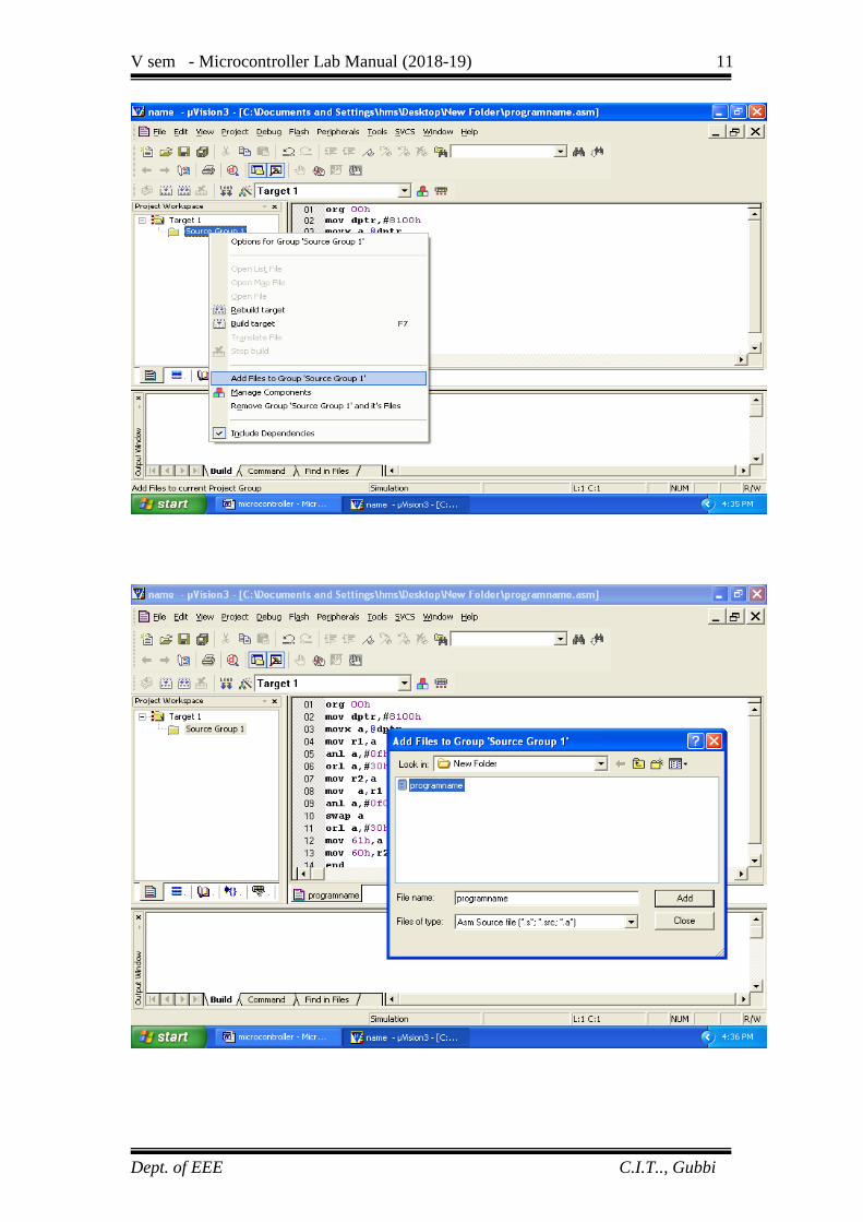
4. Create a source file (using File->New), type in the assembly or C program and
save this (filename.asm/filename.c) and add this source file to the project using
either one of the following two methods. (i) Project->Manage->Components,
Environment Books->addfiles-> browse to the required file -> OK
“OR” ii) right click on the Source Group in the Project Window and the Add
Files to Group option.
5. Set the Target options using -> Project – Options for Target opens the
µ Vision2 Options for Target – Target configuration dialog. Set the Xtal
(Crystal frequency) frequency as 11.0592 MHz, and also the Options for Target
– Debug – use either Simulator / Keil Monitor- 51 driver.
6. If Keil Monitor- 51 driver is used click on Settings -> COM Port settings select
the COM Port to which the board is connected and select the baud rate as 19200
or 9600 (recommended). Enable Serial Interrupt option if the user application is
not using on-chip UART, to stop program execution.
V sem - Microcontroller Lab Manual (2018-19)
Dept. of EEE C.I.T.., Gubbi
6
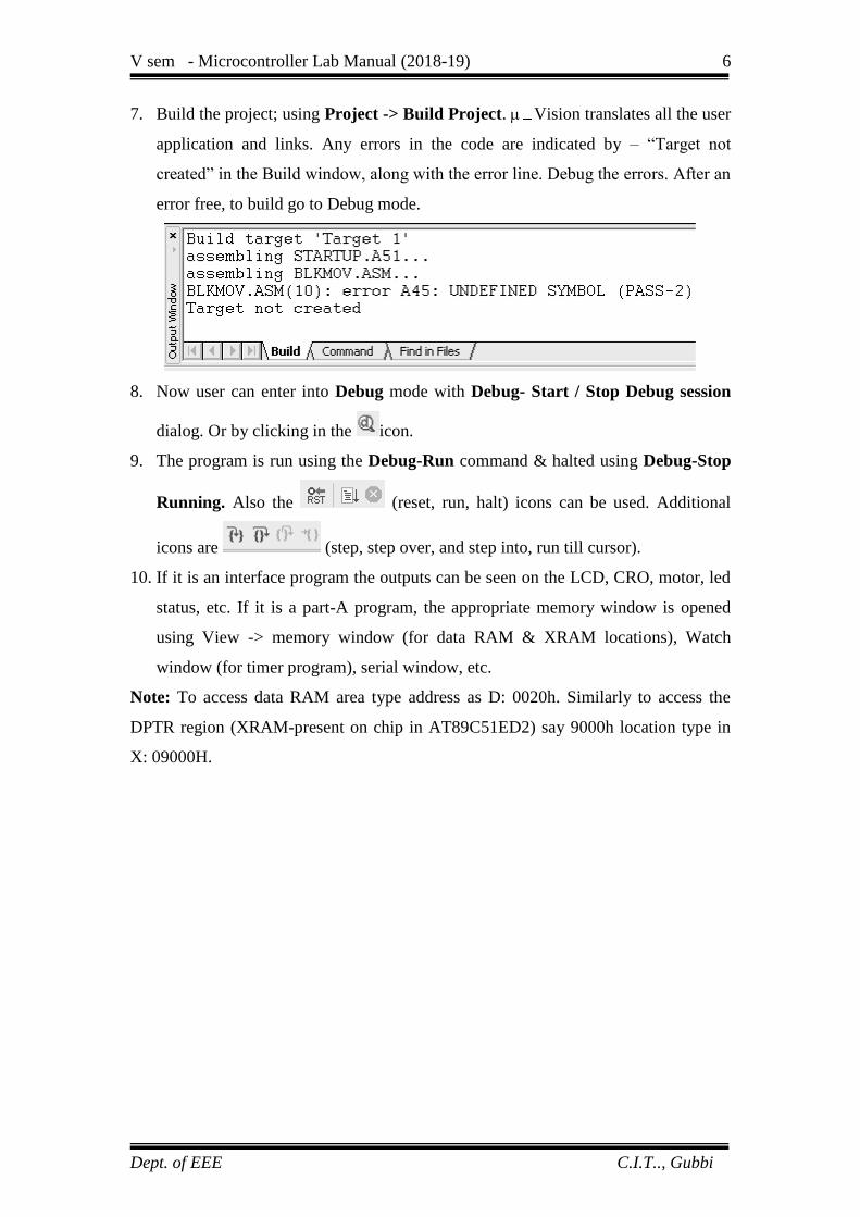
7. Build the project; using Project -> Build Project. Vision translates all the user
application and links. Any errors in the code are indicated by – “Target not
created” in the Build window, along with the error line. Debug the errors. After an
error free, to build go to Debug mode.
8. Now user can enter into Debug mode with Debug- Start / Stop Debug session
dialog. Or by clicking in the icon.
9. The program is run using the Debug-Run command & halted using Debug-Stop
Running. Also the (reset, run, halt) icons can be used. Additional
icons are (step, step over, and step into, run till cursor).
10. If it is an interface program the outputs can be seen on the LCD, CRO, motor, led
status, etc. If it is a part-A program, the appropriate memory window is opened
using View -> memory window (for data RAM & XRAM locations), Watch
window (for timer program), serial window, etc.
Note: To access data RAM area type address as D: 0020h. Similarly to access the
DPTR region (XRAM-present on chip in AT89C51ED2) say 9000h location type in
X: 09000H.

V sem - Microcontroller Lab Manual (2018-19)
Dept. of EEE C.I.T.., Gubbi
7
EXECUTION STEPS using KEIL µ vision:

V sem - Microcontroller Lab Manual (2018-19)
Dept. of EEE C.I.T.., Gubbi
8

V sem - Microcontroller Lab Manual (2018-19)
Dept. of EEE C.I.T.., Gubbi
9

V sem - Microcontroller Lab Manual (2018-19)
Dept. of EEE C.I.T.., Gubbi
10
V sem - Microcontroller Lab Manual (2018-19)
Dept. of EEE C.I.T.., Gubbi
11

V sem - Microcontroller Lab Manual (2018-19)
Dept. of EEE C.I.T.., Gubbi
12

V sem - Microcontroller Lab Manual (2018-19)
Dept. of EEE C.I.T.., Gubbi
13
Programming Using 8051
Basic Programs
Example 1: Program for addition of two 8 bit no's
mov r0,#82h ; move 10h to r0 reg
mov a, r0 ; move content r0 reg to accumalator
mov r1,#02h ; move 02h to r1 reg
mov b,r1 ; move the content of r1 reg to register b
add a,b ; add acc with reg b and stores Output in accumalator
mov 60h,a ; store Output in the data address (say 60h)
end
Output: D:60h=12
Example 2: Program for addition of two 16 bit no's
Clr c ; clear carry
mov r0,#11h ; get first lower bit no in r0
mov a,r0 ; copy ro to accumulator
mov r1,#11h ; get second lower bit no in r1
add a, r1 ; add these two no.
mov 21h, a ; store the Output
mov r5,#44h ; get first higher bit no in r5
mov a, r5 ; copy first higher byte no to accumulator
mov r6,#55h ; Get the second higher byte data in r6
addc a, r6 ; add with carry
mov 22h,c ; Store carry in 22h data location
mov 20h, a ; store the Output in data location 22h
end
output: 44 11 r5 r0
+ 55 11 + r6 r2
--------------- ---------
9922
------------- ----------

V sem - Microcontroller Lab Manual (2018-19)
Dept. of EEE C.I.T.., Gubbi
14
Example 3: Program for swap function (inter changing the nibbles)
mov a,#21h
mov 30h,a
swap a ; interchanging lower nibble to higher
mov 31h,a
end
Output: Initially acc=21
After execution acc=12
Example 4: Program for rotate operations
mov a,#21h
clr c
mov b,a
rl a ; rotate accumulator by left
mov 30h,a
mov a,b
rlc a ; rotate accumulator by left through carry
mov 31h,a
mov a,b
rr a ; rotate accumulator by right
mov 32h,a
mov a,b
rrc a ; rotate accumulator by right through carry
mov 33h,a
end
Output: Initially acc=21h
rl (d:30h)=42h
rlc(d:31h)=42h
rr(d:32h)=90h
rrc(d:33h)=10h

V sem - Microcontroller Lab Manual (2018-19)
Dept. of EEE C.I.T.., Gubbi
15
Example 5: Program for subtraction of two 8 bit no's
Mov r0,#12h ; get first no in ro
Mov a,ro ; copy to accumulator
Mov r1,#08h ; get second no
Subb a, r6 ; subtract accumulator with register r6
Mov 20h, a ; store the Output
end
Output: acc=12h
r6 =08h
---------------
D:20h= 04h
----------------
Example 6: Program for subtraction of two 16 bit no's
Clr c ; clear carry
mov r0,#11h ; get first lower bit no in r0
mov a,r0 ; copy r0 to accumulator
mov r1,#11h ; get second lower bit no in r1
subb a, r1 ; subtract these two no
mov 21h, a ; store the Output
mov r5,#44h ; get first higher bit no in r5
mov a, r5 ; copy first higher byte no to accumulator
mov r6,#55h ; Get the second higher byte data in r6
subb a, r6 ; subtract with barrow
mov 20h, a ; store the Output in data location 22h
end
output: 55 22 r5 r0
- 44 1A - r6 r2
--------------- ---------
1108
------------- ----------
V sem - Microcontroller Lab Manual (2018-19)
Dept. of EEE C.I.T.., Gubbi
16
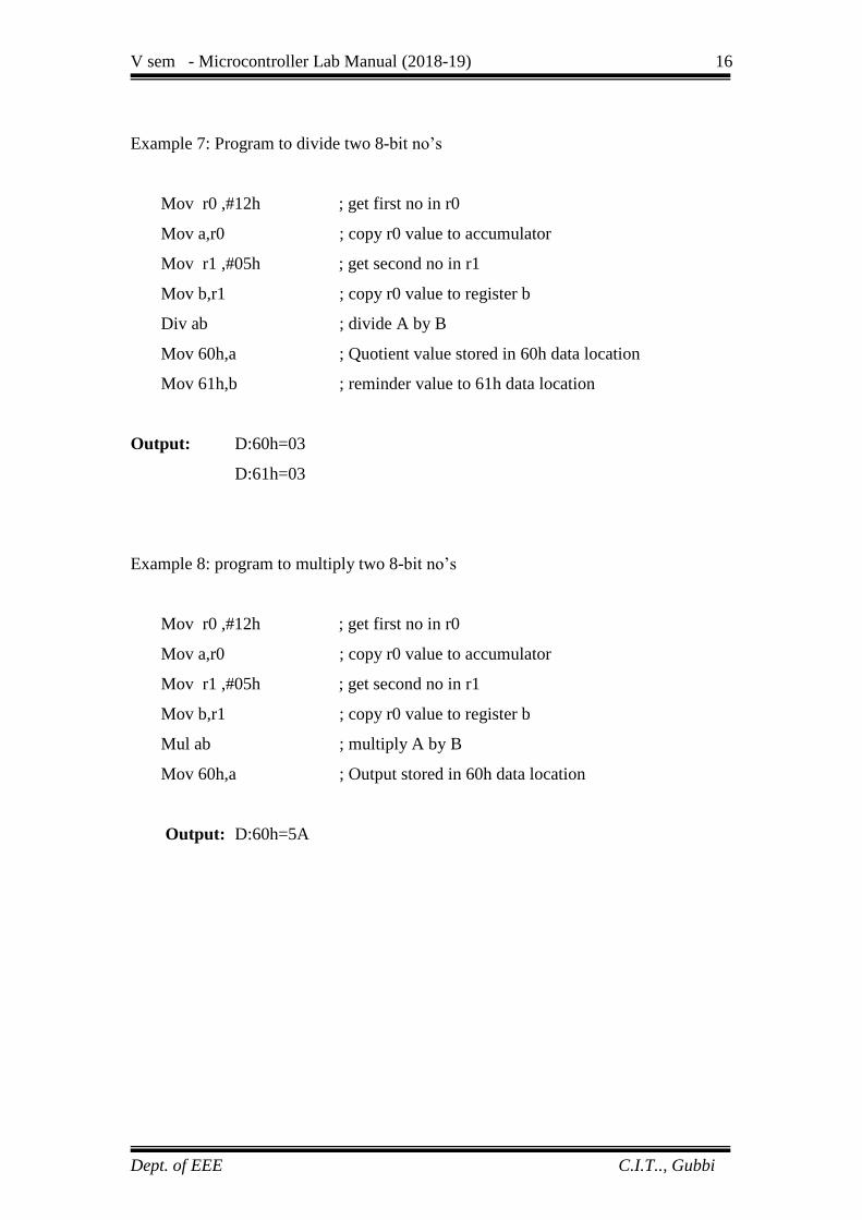
Example 7: Program to divide two 8-bit no’s
Mov r0 ,#12h ; get first no in r0
Mov a,r0 ; copy r0 value to accumulator
Mov r1 ,#05h ; get second no in r1
Mov b,r1 ; copy r0 value to register b
Div ab ; divide A by B
Mov 60h,a ; Quotient value stored in 60h data location
Mov 61h,b ; reminder value to 61h data location
Output: D:60h=03
D:61h=03
Example 8: program to multiply two 8-bit no’s
Mov r0 ,#12h ; get first no in r0
Mov a,r0 ; copy r0 value to accumulator
Mov r1 ,#05h ; get second no in r1
Mov b,r1 ; copy r0 value to register b
Mul ab ; multiply A by B
Mov 60h,a ; Output stored in 60h data location
Output: D:60h=5A

V sem - Microcontroller Lab Manual (2018-19)
Dept. of EEE C.I.T.., Gubbi
17
Example 9: Program AND, SWAP, OR operations
Mov r0 ,#12h ; get first no in r0
Mov a,r0 ; copy r0 value to accumulator
Anl a, #0F0h ; mask lower bit
Mov 60h,a ; store Output of AND operation in 60h data location
Mov a ,r0 ; copy r0 value to accumulator
Swap a ; exchange upper and lower nibbles of acc
Mov 61h,a ;store Output of AND operation in 61h data location
Mov a ,r0 ; copy r0 value to accumulator
Orl a, 0f0h ; OR operation
Mov 62h,a ;store Output of OR operation in 62h data location
End
Output: D:60h=10
D:61h=21
D:62h=12

V sem - Microcontroller Lab Manual (2018-19)
Dept. of EEE C.I.T.., Gubbi
18
V sem - Microcontroller Lab Manual (2018-19)
Dept. of EEE C.I.T.., Gubbi
19
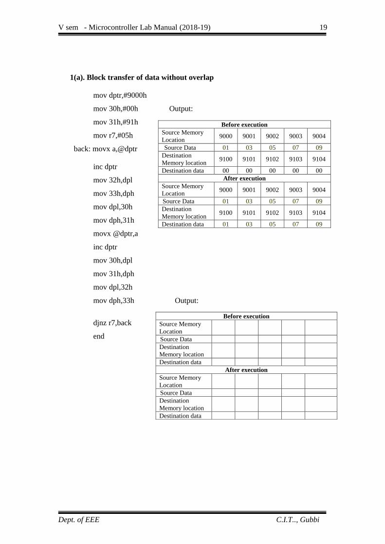
1(a). Block transfer of data without overlap
mov dptr,#9000h
mov 30h,#00h Output:
mov 31h,#91h
mov r7,#05h
back: movx a,@dptr
inc dptr
mov 32h,dpl
mov 33h,dph
mov dpl,30h
mov dph,31h
movx @dptr,a
inc dptr
mov 30h,dpl
mov 31h,dph
mov dpl,32h
mov dph,33h Output:
djnz r7,back
end
Before execution
Source Memory
Location 9000 9001 9002 9003 9004
Source Data 01 03 05 07 09
Destination
Memory location 9100 9101 9102 9103 9104
Destination data 00 00 00 00 00
After execution
Source Memory
Location 9000 9001 9002 9003 9004
Source Data 01 03 05 07 09
Destination
Memory location 9100 9101 9102 9103 9104
Destination data 01 03 05 07 09
Before execution
Source Memory
Location
Source Data
Destination
Memory location
Destination data
After execution
Source Memory
Location
Source Data
Destination
Memory location
Destination data

V sem - Microcontroller Lab Manual (2018-19)
Dept. of EEE C.I.T.., Gubbi
20
Date:
1. Data transfer – Program for block data movement, sorting,
exchanging, finding largest element in an array.
a) Block transfer of data without overlap
b) Sorting of data
c) Block exchange of data
d) Finding largest number in the array
Procedure:
• Double click Kiel μvision
• Go to project Select→ Create New project
• Select Atmel AT89C51ED2 IDE from the Kiel μvision
• Select New file , Enter the program and Save as ( . asm in Assembly and .c in
C ) and Click→ok
• Add above file to the project created, build target , debug and run the program
• observe the result , by giving particular input before execution.
Signature of Staff
V sem - Microcontroller Lab Manual (2018-19)
Dept. of EEE C.I.T.., Gubbi
21
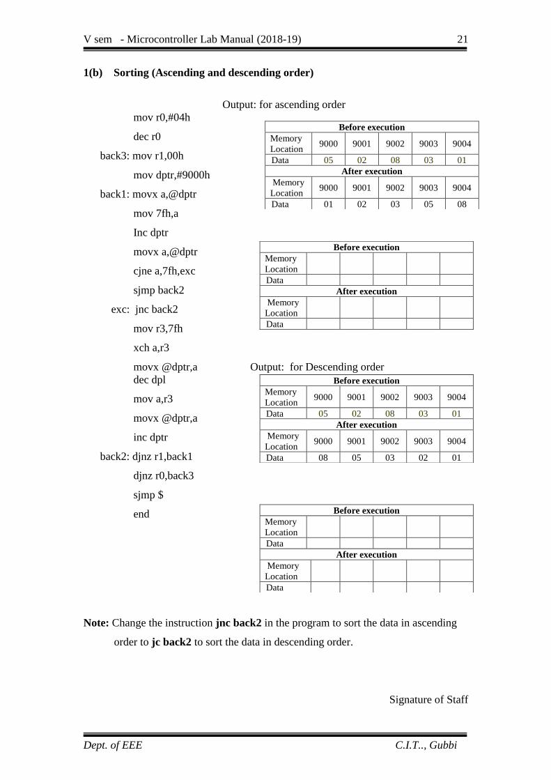
1(b) Sorting (Ascending and descending order)
Output: for ascending order
mov r0,#04h
dec r0
back3: mov r1,00h
mov dptr,#9000h
back1: movx a,@dptr
mov 7fh,a
Inc dptr
movx a,@dptr
cjne a,7fh,exc
sjmp back2
exc: jnc back2
mov r3,7fh
xch a,r3
movx @dptr,a Output: for Descending order
dec dpl
mov a,r3
movx @dptr,a
inc dptr
back2: djnz r1,back1
djnz r0,back3
sjmp $
end
Note: Change the instruction jnc back2 in the program to sort the data in ascending
order to jc back2 to sort the data in descending order.
Signature of Staff
Before execution
Memory
Location 9000 9001 9002 9003 9004
Data 05 02 08 03 01
After execution
Memory
Location 9000 9001 9002 9003 9004
Data 01 02 03 05 08
Before execution
Memory
Location
Data
After execution
Memory
Location
Data
Before execution
Memory
Location 9000 9001 9002 9003 9004
Data 05 02 08 03 01
After execution
Memory
Location 9000 9001 9002 9003 9004
Data 08 05 03 02 01
Before execution
Memory
Location
Data
After execution
Memory
Location
Data

V sem - Microcontroller Lab Manual (2018-19)
Dept. of EEE C.I.T.., Gubbi
22
Date:
1(c) Block exchange of data
mov dptr,#9000h
mov 30h,#00h
mov 31h,#91h Output:
mov r7,#05h
back: movx a,@dptr
mov 32h,dpl
mov 33h,dph
mov r4,a
mov dpl,30h
mov dph,31h
movx a,@dptr
xch a,r4
movx @dptr,a
inc dptr
mov 30h,dpl
mov 31h,dph
mov dpl,32h
mov dph,33h
mov a,r4
movx @dptr,a
inc dptr
djnz r7,back
end
Signature of Staff
Before execution
Source Memory
Location 9000 9001 9002 9003 9004
Source Data 01 02 03 04 05
Destination
Memory location 9100 9101 9102 9103 9104
Destination data 06 07 08 09 10
After execution
Source Memory
Location 9000 9001 9002 9003 9004
Source Data 06 07 08 09 10
Destination
Memory location 9100 9101 9102 9103 9104
Destination data 01 02 03 04 05
Before execution
Source Memory
Location
Source Data
Destination
Memory location
Destination data
After execution
Source Memory
Location
Source Data
Destination
Memory location
Destination data
V sem - Microcontroller Lab Manual (2018-19)
Dept. of EEE C.I.T.., Gubbi
23
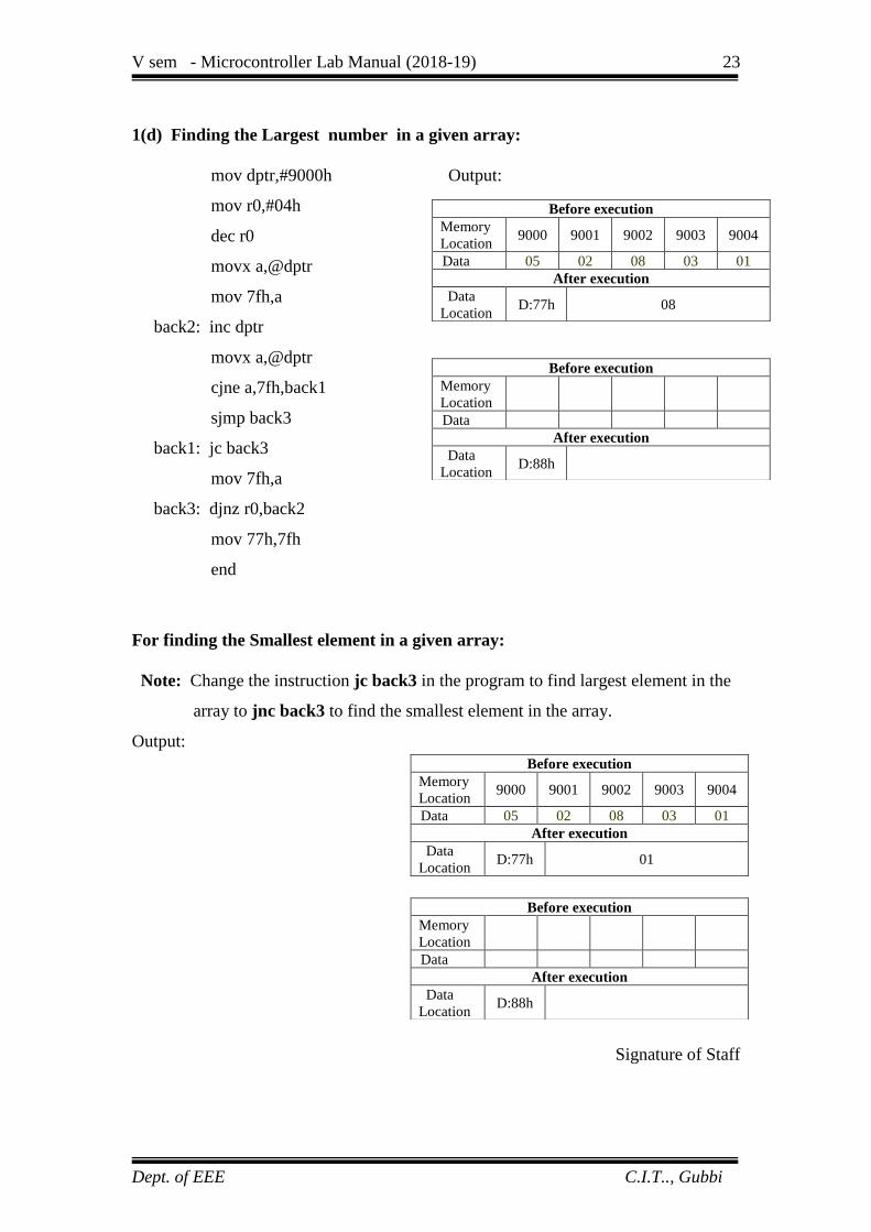
1(d) Finding the Largest number in a given array:
mov dptr,#9000h Output:
mov r0,#04h
dec r0
movx a,@dptr
mov 7fh,a
back2: inc dptr
movx a,@dptr
cjne a,7fh,back1
sjmp back3
back1: jc back3
mov 7fh,a
back3: djnz r0,back2
mov 77h,7fh
end
For finding the Smallest element in a given array:
Note: Change the instruction jc back3 in the program to find largest element in the
array to jnc back3 to find the smallest element in the array.
Output:
Signature of Staff
Before execution
Memory
Location 9000 9001 9002 9003 9004
Data 05 02 08 03 01
After execution
Data
Location D:77h 08
Before execution
Memory
Location
Data
After execution
Data
Location D:88h
Before execution
Memory
Location 9000 9001 9002 9003 9004
Data 05 02 08 03 01
After execution
Data
Location D:77h 01
Before execution
Memory
Location
Data
After execution
Data
Location D:88h

V sem - Microcontroller Lab Manual (2018-19)
Dept. of EEE C.I.T.., Gubbi
24
2 (a) Addition of two 16 bit numbers:
mov dptr,#9001h
mov r0,#0ffh
mov r1,#0ffh
mov r2,#0ffh
mov r3,#0ffh
clr c
mov a,r0
add a,r2
movx @dptr,a
dec dpl
mov a,r1
addc a,r3
movx @dptr,a
mov 00h,c
sjmp $
end
Output: r1 r0
+ r3 r2
-----------
---------------

V sem - Microcontroller Lab Manual (2018-19)
Dept. of EEE C.I.T.., Gubbi
25
2. Arithmetic instructions: Addition, subtraction, multiplication and
division. Square and cube operations for 16 bit numbers.
2(a) Addition
2(b) Subtraction
2(c ) Multiplication
2(d) Division
2(e) Square of a number
2(f) Cube of a number
Procedure:
• Double click Kiel μvision
• Go to project Select→ Create New project
• Select Atmel AT89C51ED2 IDE from the Kiel μvision
• Select New file , Enter the program and Save as ( . asm in Assembly and .c in
C ) and Click→ok
• Add above file to the project created, build target , debug and run the program
• observe the result , by giving particular input before execution.

V sem - Microcontroller Lab Manual (2018-19)
Dept. of EEE C.I.T.., Gubbi
26
2(b). Program for Subtraction of two 16 bit numbers:
mov dptr,#9001h // 5673-fc22
mov r0,#73h
mov r1,#56h
mov r2,#22h
mov r3,#0fch
clr c
mov a,r0
subb a,r2
movx @dptr,a
dec dpl
mov a,r1
subb a,r3
movx @dptr,a
mov 00h,c
end
Output: r1 r0
- r3 r2
-----------
---------------
Signature of Staff
V sem - Microcontroller Lab Manual (2018-19)
Dept. of EEE C.I.T.., Gubbi
27
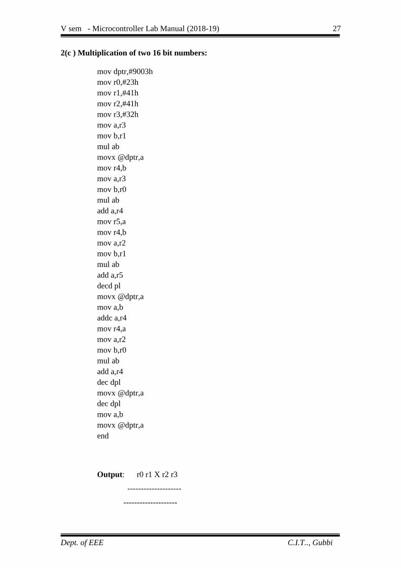
2(c ) Multiplication of two 16 bit numbers:
mov dptr,#9003h
mov r0,#23h
mov r1,#41h
mov r2,#41h
mov r3,#32h
mov a,r3
mov b,r1
mul ab
movx @dptr,a
mov r4,b
mov a,r3
mov b,r0
mul ab
add a,r4
mov r5,a
mov r4,b
mov a,r2
mov b,r1
mul ab
add a,r5
decd pl
movx @dptr,a
mov a,b
addc a,r4
mov r4,a
mov a,r2
mov b,r0
mul ab
add a,r4
dec dpl
movx @dptr,a
dec dpl
mov a,b
movx @dptr,a
end
Output: r0 r1 X r2 r3
--------------------
--------------------

V sem - Microcontroller Lab Manual (2018-19)
Dept. of EEE C.I.T.., Gubbi
28
2 (d) Division of 16 bit by 8 bit number:
org 00h
mov r0,40h
mov r1,41h
mov b,43h
mov a,r0
div ab
mov 45h,a
mov a,b
mov b,#0ah
mul ab
add a,r1
mov b,43h
div ab
mov 46h,a
here: sjmp here
end
Output: r1 r0 ÷ b
2 (e) Find square of a number:
mov dptr,#9000h
movx a,@dptr
mov b,a
mul ab
mov r0,a
mov dptr,#900eh
mov a,b
movx @dptr,a
inc dpl
mov a,r0
movx @dptr,a
end
Output: X : 900e h =(accumulator)2
V sem - Microcontroller Lab Manual (2018-19)
Dept. of EEE C.I.T.., Gubbi
29
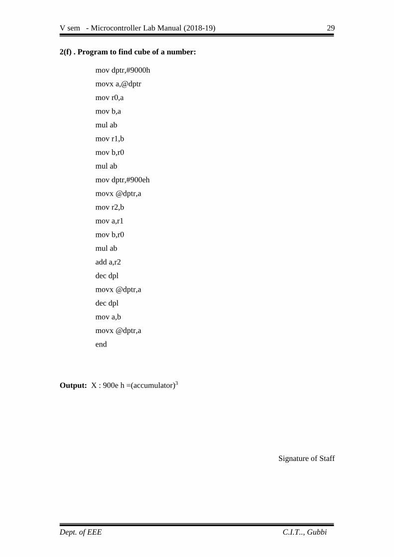
2(f) . Program to find cube of a number:
mov dptr,#9000h
movx a,@dptr
mov r0,a
mov b,a
mul ab
mov r1,b
mov b,r0
mul ab
mov dptr,#900eh
movx @dptr,a
mov r2,b
mov a,r1
mov b,r0
mul ab
add a,r2
dec dpl
movx @dptr,a
dec dpl
mov a,b
movx @dptr,a
end
Output: X : 900e h =(accumulator)3
Signature of Staff

V sem - Microcontroller Lab Manual (2018-19)
Dept. of EEE C.I.T.., Gubbi
30
3(a) Program for Binary up counter
mov dptr,#9000h
mov a,#00h
next: movx @dptr,a
acall delay
inc a
jnz next
here: sjmp here
delay: mov r1,#0ffh
loop1: mov r2,#0ffh
loop2: mov r3,#0ffh
loop3: djnz r3,loop3
djnz r2,loop2
djnz r1,loop1
ret
end
Output: x:9000h=00,01,02....ff
3( b). Program for Binary down counter
mov dptr,#9000h
mov a,#0ffh
next: movx @dptr,a
acall delay
dec a
jnz next
movx @dptr, a
here: sjmp here
delay: mov r1,#0ffh
loop1: mov r2,#0ffh
loop2: mov r3,#0ffh
loop3: djnz r3,loop3
djnz r2,loop2
djnz r1,loop1
ret
end
Output: x:9000 h= ff,fe,fd....00 Signature of Staff
V sem - Microcontroller Lab Manual (2018-19)
Dept. of EEE C.I.T.., Gubbi
31
Date:
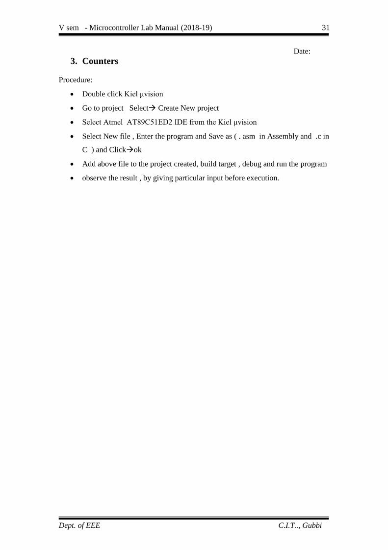
3. Counters
Procedure:
• Double click Kiel μvision
• Go to project Select→ Create New project
• Select Atmel AT89C51ED2 IDE from the Kiel μvision
• Select New file , Enter the program and Save as ( . asm in Assembly and .c in
C ) and Click→ok
• Add above file to the project created, build target , debug and run the program
• observe the result , by giving particular input before execution.
V sem - Microcontroller Lab Manual (2018-19)
Dept. of EEE C.I.T.., Gubbi
32
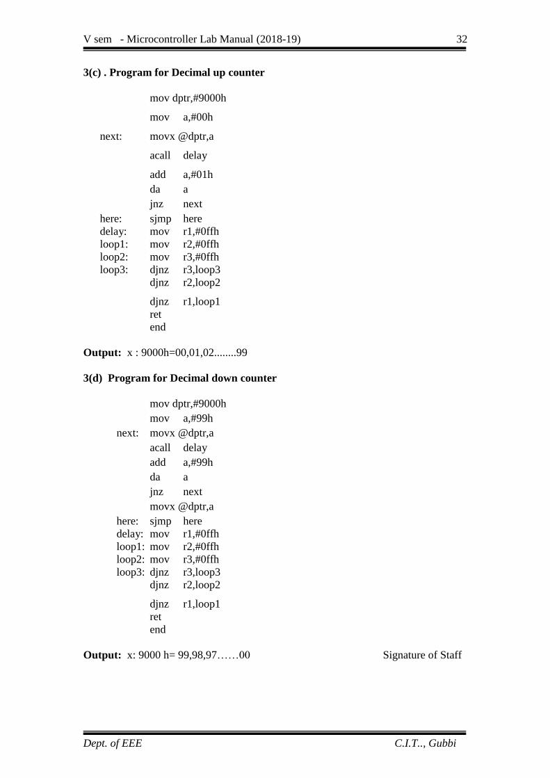
3(c) . Program for Decimal up counter
mov dptr,#9000h
mov a,#00h
next: movx @dptr,a
acall delay
add a,#01h
da a
jnz next
here: sjmp here
delay: mov r1,#0ffh
loop1: mov r2,#0ffh
loop2: mov r3,#0ffh
loop3: djnz r3,loop3
djnz r2,loop2
djnz r1,loop1
ret
end
Output: x : 9000h=00,01,02........99
3(d) Program for Decimal down counter
mov dptr,#9000h
mov a,#99h
next: movx @dptr,a
acall delay
add a,#99h
da a
jnz next
movx @dptr,a
here: sjmp here
delay: mov r1,#0ffh
loop1: mov r2,#0ffh
loop2: mov r3,#0ffh
loop3: djnz r3,loop3
djnz r2,loop2
djnz r1,loop1
ret
end
Output: x: 9000 h= 99,98,97……00 Signature of Staff

V sem - Microcontroller Lab Manual (2018-19)
Dept. of EEE C.I.T.., Gubbi
33
4. Boolean and Logical operations:
a) Write an ALP to compare two eight bit numbers NUM1 and NUM2 stored in
external memory locations 8000h and 8001h respectively. Reflect your result
as: If NUM1<NUM2, SET LSB of data RAM location 2FH (bit address 78H).
If NUM1>NUM2, SET MSB of location 2FH (bit address 7FH). If NUM1 =
NUM2, then Clear both LSB & MSB of bit addressable memory location 2FH.
mov dptr,#8000h
movx a,@dptr
mov r0,a
inc dptr
movx a,@dptr
clr c
sub a,r0
jz equal
jnc small
setb 7fh
sjmp end1
small: setb 78h
sjmp end1
equal: clr 78h
clr 7fh
end1:
end
Result:
1) Before Execution: X: 8000h = & X: 8001 =
After Execution: D: 02FH =
2) Before Execution: X: 8000h = & X: 8001 =
After Execution: D: 02FH =
3) Before Execution: X: 8000h = & X: 8001 =
After Execution: D: 02FH =

V sem - Microcontroller Lab Manual (2018-19)
Dept. of EEE C.I.T.., Gubbi
34
4. Boolean and Logical instructions (Bit Manipulation):
Procedure:
• Double click Kiel μvision
• Go to project Select→ Create New project
• Select Atmel AT89C51ED2 IDE from the Kiel μvision
• Select New file , Enter the program and Save as ( . asm in Assembly and .c in
C ) and Click→ok
• Add above file to the project created, build target , debug and run the program
• observe the result , by giving particular input before execution.

V sem - Microcontroller Lab Manual (2018-19)
Dept. of EEE C.I.T.., Gubbi
35
b. Write an assembly language program to count number of ones and
zeros in a eight bit number.
mov r1,#00h // to count number of 0s
mov r2,#00h // to count number of 1s
mov r7,#08h // counter for 8-bits
mov a,#97h // data to count number of 1s and 0s
again: rlc a
jc next
inc r1
sjmp here
next: inc r2
here: djnz r7,again
end
Result:
Input: Output:
Number of zero’s = r2 =
Number of one’s = r1
c) Write an assembly language program to find whether given eight bit
number is odd or even. If odd store 00h in accumulator. If even store FFh
in accumulator.
mov a,20h // 20h=given number, to find is it even or odd
jb acc.0,odd //jump if direct bit is set i.e., if lower bit is 1
then number is odd
mov a,#0FFh
sjmp next
odd: mov a,#00h
next:
end
Result:
Input: Output:
20h: a:

V sem - Microcontroller Lab Manual (2018-19)
Dept. of EEE C.I.T.., Gubbi
36
d. Write an assembly language program to perform logical operations AND, OR,
XOR on two eight bit numbers stored in internal RAM locations 21h, 22h.
mov a, 21h //do not use #, as data ram 21h is to be accessed
anl a, 22h //logical and operation
mov 30h, a //and operation result stored in 30h
mov a, 21h
orl a,22h //logical or operation
mov 31h, a //or operation result stored in 31h
mov a,21h
xrl a,22h //logical xor operation
mov 32h,a // xor operation result stored in 32h
end
Result:
Before Execution: D: 21H = 22H =
After Execution: D: 030H = //AND operation
D: 031H = //OR operation
D: 032H = //XOR operation
e. Write a Program to check whether given number is palindrome or not. If
palindrome store FFh in accumulator else store 00h in accumulator.
mov 30h,#81h
mov r0,30h
mov r1,#08h
mov 31h,#00h
clr c
back: mov a,30h
rlc a
mov 30h,a
mov a,31h
rrc a
mov 31h,a
djnz r1,back
cjne a,00h,npal
mov a,#0ffh
sjmp next
npal: mov a,#00h
next: end
Result:
Input: Output:

V sem - Microcontroller Lab Manual (2018-19)
Dept. of EEE C.I.T.., Gubbi
37
Conditional call and return instructions:
Ex 1: write a program to clear accumulator [a], then add 5 to the accumulator 20
times
mov a,#0
mov r2,#20
again: add a,#05
djnz r2,again
mov r5,a
Output:
Ex 2: write a program in which if R4 register contains the value 0. Then put 55H
in R4 register:
mov a,r4
jnz next
mov r4,#55h
next: mov a, r4
Output:
Ex3:
V sem - Microcontroller Lab Manual (2018-19)
Dept. of EEE C.I.T.., Gubbi
38
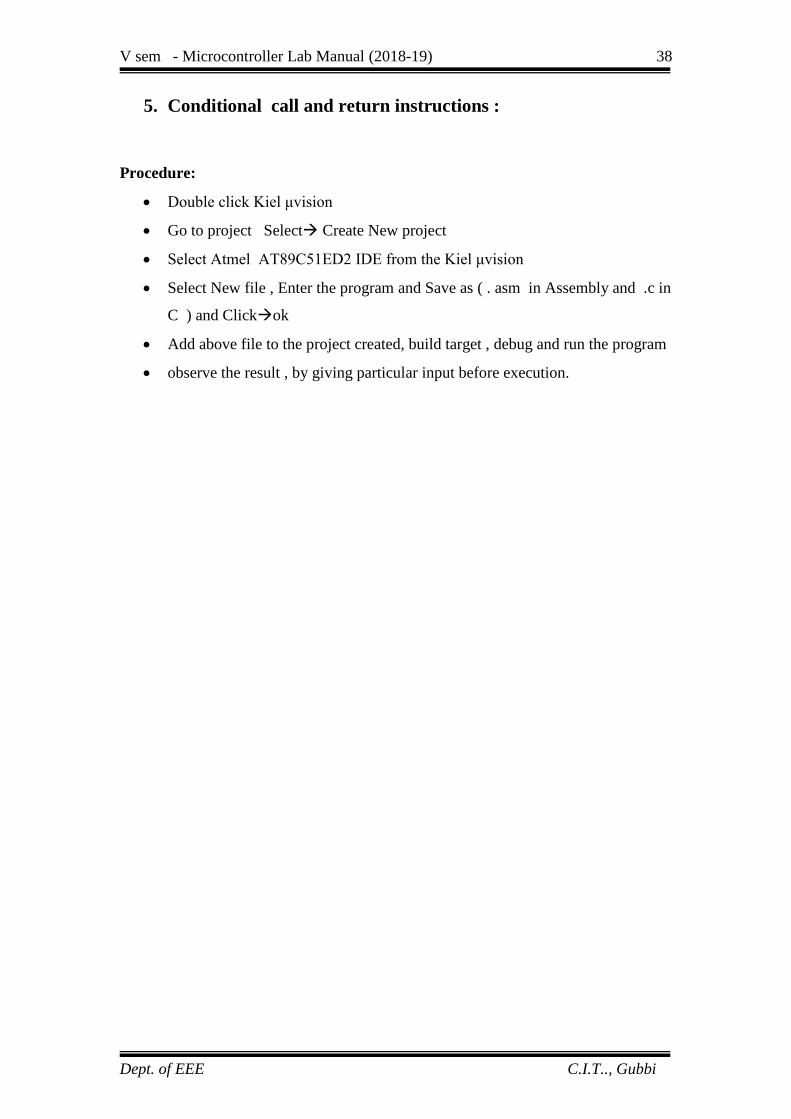
5. Conditional call and return instructions :
Procedure:
• Double click Kiel μvision
• Go to project Select→ Create New project
• Select Atmel AT89C51ED2 IDE from the Kiel μvision
• Select New file , Enter the program and Save as ( . asm in Assembly and .c in
C ) and Click→ok
• Add above file to the project created, build target , debug and run the program
• observe the result , by giving particular input before execution.

V sem - Microcontroller Lab Manual (2018-19)
Dept. of EEE C.I.T.., Gubbi
39
a) Program to convert a BCD number into ASCII code:
mov dptr,#9000h
movx a,@dptr
mov r0,a
swap a
mov dptr,#900dh
acall ascii
mov a,r0
acall ascii
sjmp $
ascii: anl a,#0fh
add a,#30h
movx @dptr,a
inc dptr
ret
end
Result:
Before execution
Memory
Location 9000 900d 900e
Data 45 00 00
After execution
Memory
Location 9000 900d 900e
Data 45 34 35
Before execution
Memory
Location 9000 900d 900e
Data 97 00 00
After execution
Memory
Location 9000 900d 900e
Data 97

V sem - Microcontroller Lab Manual (2018-19)
Dept. of EEE C.I.T.., Gubbi
40
6. Code conversion programs
a) BCD to ASCII
b) ASCII to BCD
c) ASCII to Decimal
d) Decimal to ASCII
e) Hexa to decimal
f) Decimal to Hexa
Procedure:
• Double click Kiel μvision
• Go to project Select→ Create New project
• Select Atmel AT89C51ED2 IDE from the Kiel μvision
• Select New file , Enter the program and Save as ( . asm in Assembly and .c in
C ) and Click→ok
• Add above file to the project created, build target , debug and run the program
• observe the result , by giving particular input before execution.
Signature of Staff
V sem - Microcontroller Lab Manual (2018-19)
Dept. of EEE C.I.T.., Gubbi
41
Date:
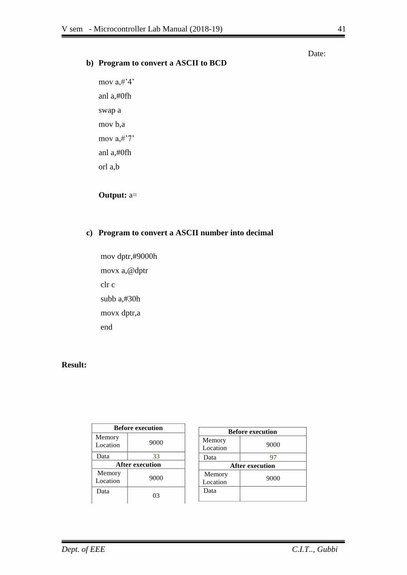
b) Program to convert a ASCII to BCD
mov a,#’4’
anl a,#0fh
swap a
mov b,a
mov a,#’7’
anl a,#0fh
orl a,b
Output: a=
c) Program to convert a ASCII number into decimal
mov dptr,#9000h
movx a,@dptr
clr c
subb a,#30h
movx dptr,a
end
Result:
Before execution
Memory
Location 9000
Data 33
After execution
Memory
Location 9000
Data 03
Before execution
Memory
Location 9000
Data 97
After execution
Memory
Location 9000
Data

V sem - Microcontroller Lab Manual (2018-19)
Dept. of EEE C.I.T.., Gubbi
42
Date:
d) Program to convert decimal number to ASCII
mov dptr,#9000h
movx a,@dptr
add a,#30h
mov dptr,#900dh
movx @dptr,a
end
Result:
Signature of Staff
Before execution
Memory
Location 9000
Data 03
After execution
Memory
Location 9000
Data 33
Before execution
Memory
Location 9000
Data 63
After execution
Memory
Location 9000
Data

V sem - Microcontroller Lab Manual (2018-19)
Dept. of EEE C.I.T.., Gubbi
43
Date:
e) Program to convert Hex number to Decimal:
org 00h
mov a,#0a9h
mov b,#0ah
div ab
mov r0,b
mov b,#0ah
div ab
mov r1,b
mov r2,a
end
Result: r0=01
r1=06
r2=09
Signature of Staff

V sem - Microcontroller Lab Manual (2018-19)
Dept. of EEE C.I.T.., Gubbi
44
Date:
f) Program to convert decimal number to HEX:
mov dptr,#9000h
movx a,@dptr
mov r0,a
anl a,#0f0h
swap a
mov b,#0ah
mul ab
mov r1,a
mov a,r0
anl a ,#0fh
add a,r1
movx @dptr,a
end
Result:
Signature of Staff
Before execution
Memory
Location 9000
Data 99
After execution
Memory
Location 9000
Data
Before execution
Memory
Location 9000
Data 55
After execution
Memory
Location 9000
Data 37

V sem - Microcontroller Lab Manual (2018-19)
Dept. of EEE C.I.T.., Gubbi
45
a) Program to configure 8051 microcontroller to transmit characters “ENTER
YOUR NAME” to a PC using the serial port and display on the serial window
mov tmod,#20h //setting Timer-1 in mode-2
mov scon,#70h
mov th1,#-3
setb tr1
again: mov r0,#03h
mov dptr,#8000h
nextchar: movx a,@dptr
acall transfer
inc dptr
djnz r0,nextchar
sjmp again
transfer: mov sbuf,a
wait: jnb ti,wait
clr ti
ret
end
RESULT:
Each time the program is executed, “ENTER YOUR NAME” will be displayed on the
serial window.
Baud rate Calculation:
Crystal freq/ (12*32) = (11.0592MHz)/(12*32) = 28800.
Serial communication circuitry divides the machine cycle frequency
(11.0592MHz)/(12) by 32 before it is being used by the timer to set the baud rate.
To get 9600, 28800/3 is obtained by loading timer1 with -3 (i.e., FF – 3 = FD) for
further clock division. For 2400 baud rate, 28800/12 => -12 = F4 in TH1.

V sem - Microcontroller Lab Manual (2018-19)
Dept. of EEE C.I.T.., Gubbi
46
7. Programs to generate delay, Programs using serial port and
on-chip timer/counters.
a) Program to configure 8051 microcontroller to transmit characters “ENTER
YOUR NAME” to a PC using the serial port and display on the serial
window.
b) Program to generate 1second delay continuously using on chip timer.
Procedure:
• Double click Kiel μvision
• Go to project Select→ Create New project
• Select Atmel AT89C51ED2 IDE from the Kiel μvision
• Select New file , Enter the program and Save as ( . asm in Assembly and .c in
C ) and Click→ok
• Add above file to the project created, build target , debug and run the program
• observe the result , by giving particular input before execution.
Note: To use result of this program, after selecting DEBUG session in the
main menu use View-> serial window #1. On running & halting the program, the data
is seen in the serial window.

V sem - Microcontroller Lab Manual (2018-19)
Dept. of EEE C.I.T.., Gubbi
47
b. Program to generate 1second delay continuously using on chip timer.
mov tmod,#02h
mov th0,#00h
clr P1.0
clr a
setb tr0
again: mov r7,#0ffh
loop: mov r6,#14d
wait: jnb tf0, wait
clr tf0
djnz r6,wait
djnz r7,loop
cpl P1.0
sjmp again
end
RESULT:
Accumulator A is incremented in binary from 00, 01,02…09,0A, 0B, …, 0F, 10, 11,
…FF every 1 second (for 33MHz clock setting & every 3 seconds for 11.0598MHz)
V sem - Microcontroller Lab Manual (2018-19)
Dept. of EEE C.I.T.., Gubbi
48

V sem - Microcontroller Lab Manual (2018-19)
Dept. of EEE C.I.T.., Gubbi
49
8. Program for stepper motor interface.
Block Diagram:
#include <REG51xD2.H>
void delay (unsigned int x) /* Delay Routine */
{
for(;x>0;x--);
return;
}
main ( )
{
unsigned char Val, i;
P0=0x00;
while(1)
{
Val = 0x11;
for (i=0;i<4;i++)
{
P0 = Val;
Val = Val<<1; /* Val= Val>>1; for clockwise direction*/
delay (500);
}
}
}
Signature of Staff
8
0 P 0.0
5 P 0.7
1
Stepper
Motor
Interfacing
Control
Stepper
Motor

V sem - Microcontroller Lab Manual (2018-19)
Dept. of EEE C.I.T.., Gubbi
50
Date:
9. Program for Dc motor interface for direction and speed control
using PWM.
Block Diagram:
This program measures the motor speed and displays it on LCD
This Program uses Po for DAC data i.e. for speed increment or decrement
#include <REG51xD2.H>
sbit inr= P3^2; //speed increment switch
sbit dcr= P3^3; //speed decrement switch
main()
{
unsigned char i=0x80;
P0 = 0x7f; /*Run the motor at half speed.*/
while (1)
{ if (!inr)
{while (!inr);
if(i>10)
i=i-10; //increase the DC motor speed
}
if(!dcr)
{
while(!dcr);
if(i<0xf0)
i=i+10; //decrease the DC motor speed
}
P0=i;
}
}
Signature of Staff

V sem - Microcontroller Lab Manual (2018-19)
Dept. of EEE C.I.T.., Gubbi
51
Date:
10. Program to interface Alphanumerical LCD panel and Hex
keypad to 8051.
Block diagram :
LABEL ON THE HEX LABEL ON THE HEX
KEYTOP CODE KEYTOP CODE
0 0 - 0C 1 1 * 0D 2 2 / 0E 3 3 % 0F 4 4 AC 10 5 5 CE 11 6 6 CHK 12 7 7 = 13 8 8 MC 14 9 9 MR 15 . 0A M 16
+ 0B M+ 17
#include <REG51xD2.H>
#include "lcd.h"
unsigned char getkey();
void delay(unsigned int);
main()
{
unsigned char key,tmp;

V sem - Microcontroller Lab Manual (2018-19)
Dept. of EEE C.I.T.., Gubbi
52
InitLcd(); /* Initialise LCD */
WriteString("Key Pressed="); /* Display msg on LCD */
while(1)
{
GotoXY(12,0); /* Set Cursor Position */
key = getkey(); /* Call Getkey method */
}
}
unsigned char getkey()
{
unsigned char i,j,k,indx,t;
P2 = 0x00; /* P2 as Output port */
indx = 0x00; /* Index for storing the first value of
the scanline */
for(i=1;i<=8;i<<=1) /* for 4 scanlines */
{
P1 = 0x0f & ~i; /* write data to scanline */
t = P0; /* Read readlines connected to P0*/
t = ~t;
if(t>0) /* If key press is true */
{
delay(6000); /* Delay for bouncing */
for(j=0;j<=4;j++) /* Check for 8 lines */
{
t >>=1;
if(t==0) /* if get pressed key*/
{
k = indx+j; /* Display that by converting to Ascii */
if(k > 9)
k+=0x37;
else
k+=0x30;
WriteChar(k);
return(indx+j); /* Return index of the key pressed */
}
}
}
indx += 0x04; /* If no key pressed increment index */
}
}
void delay(unsigned int x) /* delay routine */
{
for(;x>0;x--);
}
Signature o Staff

V sem - Microcontroller Lab Manual (2018-19)
Dept. of EEE C.I.T.., Gubbi
53
Date:
11. (a) Program for dual DAC interfacing to generate square wave of
frequency ‘f’.
Block Diagram:
#include <REG51xD2.H>
sbit Amp = P3^3; /* Port line to change amplitude */
sbit Fre = P3^2; /* Port line to change frequency */
void delay(unsigned int x) /* delay routine */
{
for(;x>0;x--);
}
main()
{
unsigned char on = 0x7f,off=0x00;
unsigned int fre = 100;
while(1)
{
if(!Amp) /* if user choice is to change amplitude */
{
while(!Amp); /* wait for key release */
on+=0x08; /* Increase the amplitude */
}
if(!Fre) /* if user choice is to change frequency */
{
if(fre > 1000) /* if frequency exceeds 1000 reset to default */
fre = 100;

V sem - Microcontroller Lab Manual (2018-19)
Dept. of EEE C.I.T.., Gubbi
54
while(!Fre); /* wait for key release */
fre += 50; /* Increase the frequency */
}
P0=on; /* write apmlitude to port */
delay(fre);
P0 = off; /* clear port */
delay(fre);
}
}

V sem - Microcontroller Lab Manual (2018-19)
Dept. of EEE C.I.T.., Gubbi
55
Date:
11(b). Program for dual DAC interfacing to generate ramp
waveform.
Block Diagram:
#include <REG51xD2.H>
main()
{
unsigned char i=0;
P0 = 0x00; /* P0 as Output port */
while(1)
{
{
for(i=0;i<0xff;i++) /* Generate ON pulse */
P0 = i;
}
}
V sem - Microcontroller Lab Manual (2018-19)
Dept. of EEE C.I.T.., Gubbi
56
Date:
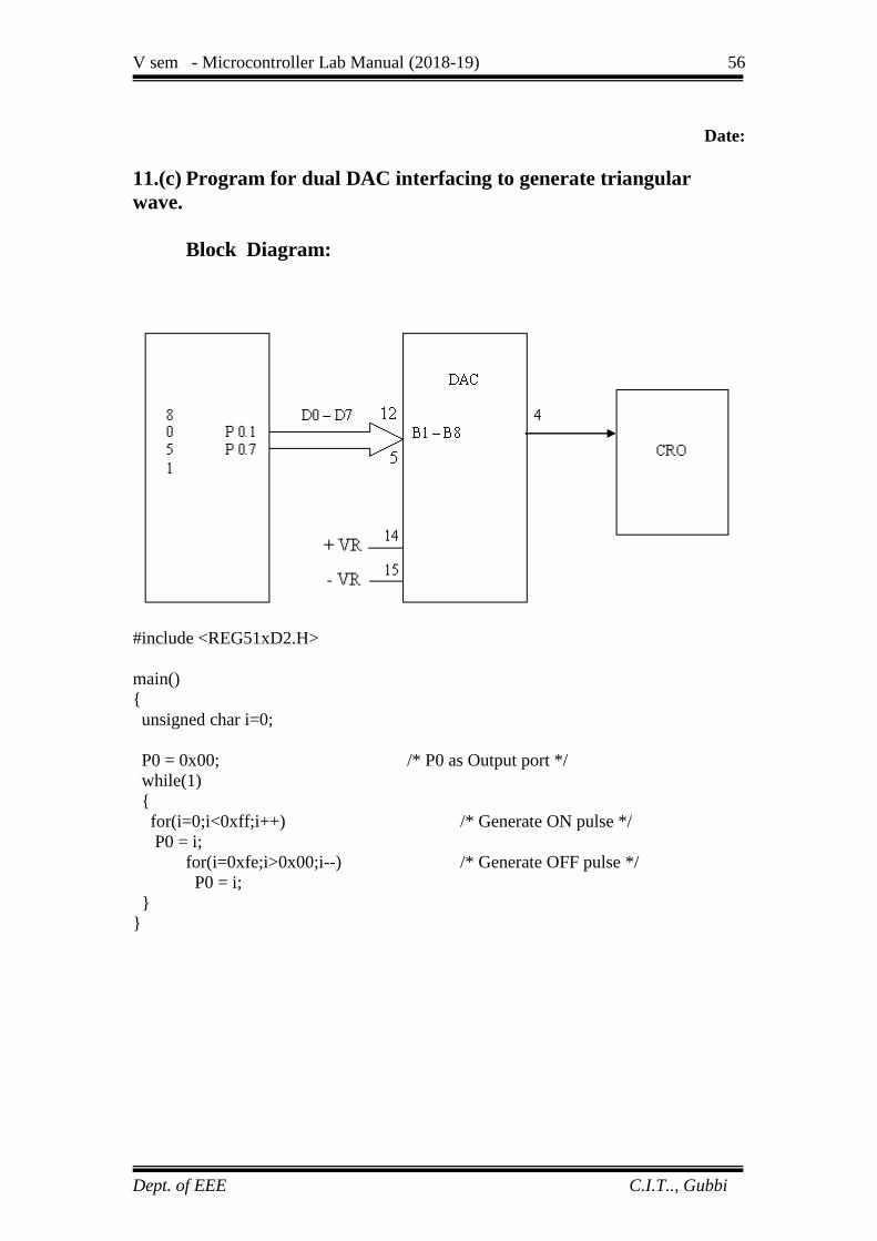
11.(c) Program for dual DAC interfacing to generate triangular
wave.
Block Diagram:
#include <REG51xD2.H>
main()
{
unsigned char i=0;
P0 = 0x00; /* P0 as Output port */
while(1)
{
for(i=0;i<0xff;i++) /* Generate ON pulse */
P0 = i;
for(i=0xfe;i>0x00;i--) /* Generate OFF pulse */
P0 = i;
}
}

V sem - Microcontroller Lab Manual (2018-19)
Dept. of EEE C.I.T.., Gubbi
57
Date:
11.(d) Program for dual DAC interfacing to generate sine waveform.
Circuit Diagram:
,
#include <RE51xD2.H>
void main( )
{
unsigned char i,
wave[36]={128,148,171,192,209,225,238,245,253,255,253,
245,238,225,209,192,171,128,104,82,64,43,28,15,07,01,00,01,07,15,28,43,64,82,104
};
P0 = 0x00;
while(1)
{
for (i==0; i<12; i++)
P0= i;
}
}

V sem - Microcontroller Lab Manual (2018-19)
Dept. of EEE C.I.T.., Gubbi
58
Date:
12. External ADC and temperature control interface.
# include <at89c51xd2.h>
#include<intrins.h>
#include "lcd.h"
unsigned int Adc;
unsigned char Low_adc,High_adc,relay; read_adc()
{
unsigned char status;
P2_3 = 1 ; // Start conversion of ADC
status = P1; //Read status of ADC
while((status & 0x01) != 0x01)
{
status = P1;
}
P2_2 = 0; // Enable outputs
P2_0 = 0; // Activate B1 to B8 outputs
Low_adc = P0; // Read lower byte of ADC and place in R0
P2_0 = 1; // Deactivate B1 to B8 outputs
P2_1 = 0; // Activate B9 to B12 and POL, over range
outputs High_adc = P0; // Read higher byte of ADC
High_adc = High_adc & 0x0F;
P2_1 = 1; // deactivate B9 to B12 and POL, over range outputs
P2_2 = 1; // Disable outputs
P2_3 = 0; // Stop conversion of ADC
}
main()
{
float Temp,Vol,Res;
unsigned char Temp1;
unsigned char Temp2,Temp3;
P0 = 0xFF ; // Make port 0 as input
P2 = 0xFF ; // Make port 2 as high now the relay is on.
P1_1 = 0 ; // switch OFF relay
P2_3 = 0 ; // STOP conversion of ADC
relay = 10;

V sem - Microcontroller Lab Manual (2018-19)
Dept. of EEE C.I.T.., Gubbi
59
while(1)
{
read_adc(); //Read ADC
Adc = High_adc;
Adc <<= 8;
Adc = Adc | Low_adc;
if( (Adc > 0x656) && (relay != 0)) //IF greater than 0x0656 Switch OFF relay
{
ClrLcd();
WriteString("RELAY OFF");
P1_1 = 0 ;
relay = 0;
}
else if ( (Adc < 0x5b9) && (relay!= 1)) //IF less than 0x05B9 Switch ON relay
{
ClrLcd();
WriteString("RELAY ON");
P1_1 = 1 ;
relay = 1;
}
Vol =-((Adc/10)*0.000488); //voltage before amplifier
Res =((100*(1.8-Vol)-100*Vol)*100) /(100*Vol + 100*(1.8+Vol));
//Resistance Value
Res = Res - 100;
Temp = Res/ 0.384;
Temp1 = Temp;
Temp2 = 0x30 + (Temp1 / 0x0A);
Temp3 = 0x30 + (Temp1 % 0x0A);
GotoXY(0,1);
WriteString("Temperature ");
WriteChar(Temp2);
WriteChar(Temp3);
WriteString("'C");
}
}

V sem - Microcontroller Lab Manual (2018-19)
Dept. of EEE C.I.T.., Gubbi
60
Date:
13. Program for Elevator interface.
#include <REG51D2.H>
void delay(unsigned int);
main()
{
unsigned char Flr[9] = {0xff,0x00,0x03,0xff,0x06,0xff,0xff,0xff,0x09};
unsigned char FClr[9] = {0xff,0x0E0,0x0D3,0xff,0x0B6,0xff,0xff,0xff,0x79};
unsigned char ReqFlr,CurFlr = 0x01,i,j;
P0 = 0x00;
P0 = 0x0f0;
while(1)
{
P1 = 0x0f;
ReqFlr = P1 | 0x0f0;
while(ReqFlr == 0x0ff)
ReqFlr = P1 | 0x0f0; /* Read Request Floor from P1 */
ReqFlr = ~ReqFlr;
if(CurFlr == ReqFlr) /* If Request floor is equal to Current Floor */
{
P0 = FClr[CurFlr]; /* Clear Floor Indicator */
continue; /* Go up to read again */
}
else if(CurFlr > ReqFlr) /* If Current floor is > request floor */
{

V sem - Microcontroller Lab Manual (2018-19)
Dept. of EEE C.I.T.., Gubbi
61
13. C program to interface Elevator
E
8 L
P0
E
0 V
5 P1 A
1
T
O
R Theory:
The operation of the elevator is as follows:
Initially, the elevator is at ground floor.
When the elevator reaches any floor, it stays at that floor until a request from
another floor is made. When such a request is detected, it moves to that
floor. The floor request are scanned in fixed order i.e., floors 0, 1, 2 and 3.
This interface simulates the control and operation of an elevator. Four
floors assumed and for each floor a key and corresponding LED indicator are
provided to serve as request buttons and request status indicator. The elevator
itself is represented by a column of ten LEDs. The motion of elevator can be
simulated by turning on successive LEDs one at a time. Te delay between
turning off one LED and turning on the next LED can simulate the “speed” of
the elevator. User can read the request status information through one port,
reset the request indicators through another port and control the elevator (LED
column) through another port.
Description of the Circuit
This interface has four keys, marked 0, 1, 2, and 3 representing the
request buttons at the four floors. Pressing of key causes a corresponding Flip-
Flop to be set. The outputs of the four Flip-flops can be read through port B
(PBO, PBI, PB2 and PB3). Also, the status of these signals is reflected by a
setoff 4 LEDs. The Flip-Flop can be rest (LEDs are cleared) through port
A(PA54, PA5, PA6, and PA7). A column of 10 LEDs, representing the
elevator can be controlled through Port A (PA0, PA1, PA2 and PA3). These
port lines

V sem - Microcontroller Lab Manual (2018-19)
Dept. of EEE C.I.T.., Gubbi
62
i = Flr[CurFlr] - Flr[ReqFlr]; /* Get the no of floors to travel */
j = Flr[CurFlr];
for(;i>0;i--) /* Move the indicator down */
{
P0 = 0x0f0|j;
j--;
delay(50000);
}
}
else /* If Current floor is < request floor */
{
i = Flr[ReqFlr] - Flr[CurFlr]; /* Get the no of floors to travel */
j = Flr[CurFlr];
for(;i>0;i--) /* Move the indicator Up */
{
P0 = 0x0f0 | j;
j++;
delay(50000);
}
}
CurFlr = ReqFlr; /* Update Current floor */
P0 = FClr[CurFlr]; /* Clear the indicator */
}
}
void delay(unsigned int x)
{
for(;x>0;x--);
}

V sem - Microcontroller Lab Manual (2018-19)
Dept. of EEE C.I.T.., Gubbi
63
are fed to the inputs of the decoder 7442 whose outputs are used to control the
on/off states of the LEDs which simulate the motion of the elevator.

V sem - Microcontroller Lab Manual (2018-19)
Dept. of EEE C.I.T.., Gubbi
64
Question bank Part A:
1. Write an assembly language program to transfer N = _______ bytes of data from
location A : _______h to location B: _________h (without overlap) using 8051
2. Write an assembly language program to exchange N = _______ bytes of data from
location A : _______h to location B: _________h (without overlap) using 8051
3. Write an assembly language program to sort an array of N = ______h bytes of data
in ascending /descending order using 8051
4. Write an assembly language program to find largest number in a given array of ‘N’
elements using 8051 , where , N =_____h
5. Write an assembly language program to perform addition of two 16 bit numbers
using 8051
6. Write an assembly language program to perform subtraction of two 16 bit numbers
using 8051
7. Write an assembly language program to perform multiplication of two 16 bit
numbers using 8051
8. Write an assembly language program to perform division of two 16 bit numbers
using 8051
9. Write an assembly language program to find square of a given numbers using 8051
10. Write an assembly language program to find cube of a given numbers using 8051
11. Write an assembly language program to count numbers from N =___h to
N=______h (Up counter/Down counter ) using 8051
12. Write an assembly language program to implement(display) an eight bit
Up /Down binary(hex) counter on watch window using 8051
13. Write an assembly language program to count number of one’s and zero’s in given
8 bit number using 8051
14. Write an assembly language program to exhibit the usage of call and return
instruction
15. Write an assembly language program to convert an 8 bit BCD number to ASCII
using 8051
16. Write an assembly language program to convert ASCII to an 8 bit BCD number to
using 8051
17. Write an assembly language program to convert ASCII to decimal using 8051
18. Write an assembly language program to convert decimal to ASCII using 8051
19. Write an assembly language program to convert Hexa decimal to decimal using
8051
20. Write an assembly language program to convert decimal to Hexa decimal using
8051
21. Write an assembly language program to generate delay of _____seconds using
8051
Part B(using C program)
A. Write a program for stepper motor interface with 8051
B. Write a program for DC motor interface with 8051 and control its speed
C. Write a program to interface LCD panel and hexa keypad to 8051
D. Write a program for dual DAC interfacing to generate sine wave
E. Write a program for dual DAC interfacing to generate square wave
F. Write a program for dual DAC interfacing to generate triangular wave
G. Write a program for dual DAC interfacing to generate ramp wave
H. Write a program to interface ADC with 8051
I. Write a program for elevator interface with 8051

V sem - Microcontroller Lab Manual (2018-19)
Dept. of EEE C.I.T.., Gubbi
65
Viva Questions
1. What do you mean by Embedded System? Give examples.
2. Why are embedded Systems useful?
3. What are the segments of Embedded System?
4. What is Embedded Controller?
5. What is Microcontroller?
6. List out the differences between Microcontroller and Microprocessor.
7. How are Microcontrollers more suitable than Microprocessor for Real Time Applications?
8. What are the General Features of Microcontroller?
9. Explain briefly the classification of Microcontroller.
10. Explain briefly the Embedded Tools.
11. Explain the general features of 8051 Microcontroller.
12. How many pin the 8051 has?
13. Differentiate between Program Memory and Data Memory.
14. What is the size of the Program and Data memory?
15. Write a note on internal RAM. What is the necessity of register banks? Explain.
16. How many address lines are required to address 4K of memory? Show the necessary
calculations.
17. What is the function of accumulator?
18. What are SFR’s? Explain briefly.
19. What is the program counter? What is its use?
20. What is the size of the PC?
21. What is a stack pointer (SP)?
22. What is the size of SP?
23. What is the PSW? And briefly describe the function of its fields.
24. What is the difference between PC and DPTR?
25. What is the difference between PC and SP?
26. What is ALE? Explain the functions of the ALE in 8051.
27. Describe the 8051 oscillator and clock.
28. What are the disadvantages of the ceramic resonator?
29. What is the function of the capacitors in the oscillator circuit?
30. Show with an example, how the time taken to execute an instruction can be calculated.
31. What is the Data Pointer register? What is its use in the 8051?
32. Explain how the 8051 implement the Harvard Architecture?
33. Explain briefly the difference between the Von Neumann and the Harvard Architecture.
34. Describe in detail how the register banks are organized.
35. What are the bit addressable registers and what is the need?
36. What is the need for the general purpose RAM area?
37. Write a note on the Stack and the Stack Pointer.
38. Why should the stack be placed high in internal RAM?
39. Explain briefly how internal and external ROM gets accessed.
40. What are the different addressing modes supported by 8051 Microcontroller ?
41. Explain the Immediate Addressing Mode.
42. Explain the Register Addressing Mode.
43. Explain the Direct Addressing Mode.
44. Explain the Indirect Addressing Mode.
45. Explain the Code Addressing Mode.
46. Explain in detail the Functional Classification of 8051 Instruction set
47. What are the instructions used to operate stack?
48. What are Accumulator specific transfer instructions?
49. What is the difference between INC and ADD instructions?
50. What is the difference between DEC and SUBB instructions?
51. What is the use of OV flag in MUL and DIV instructions?
52. What are single and two operand instructions?
53. Explain Unconditional and Conditional JMP and CALL instructions.
54. Explain the different types of RETURN instructions.
55. What is a software delay?
56. What are the factors to be considered while deciding a software delay?
57. What is a Machine cycle?

V sem - Microcontroller Lab Manual (2018-19)
Dept. of EEE C.I.T.., Gubbi
66
58. What is a State?
59. Explain the need for Hardware Timers and Counters?
60. Give a brief introduction on Timers/Counter.
61. What is the difference between Timer and Counter operation?
62. How many Timers are there in 8051?
63. What are the three functions of Timers?
64. What are the different modes of operation of timer/counter?
65. Give a brief introduction on the various Modes.
66. What is the count rate of timer operation?
67. What is the difference between mode 0 and mode 1?
68. What is the difference Modes 0,1,2 and 3?
69. How do you differentiate between Timers and Counters?
70. Explain the function of the TMOD register and its various fields?
71. How do you control the timer/counter operation?
72. What is the function of TF0/TF1 bit
73. Explain the function of the TCON register and its various fields?
74. Explain how the Timer/Counter Interrupts work.
75. Explain how the 8051 counts using Timers and Counters.
76. Explain Counting operation in detail in the 8051.
77. Explain why there is limit to the maximum external frequency that can be counted.
78. What’s the benefit of the auto-reload mode?
79. Write a short note on Serial and Parallel communication and highlight their advantages and
disadvantages.
80. Explain Synchronous Serial Data Communication.
81. Explain Asynchronous Serial Data Communication.
82. Explain Simplex data transmission with examples.
83. Explain Half Duplex data transmission with examples.
84. Explain Full Duplex data transmission with examples.
85. What is Baud rate?
86. What is a Modem?
87. What are the various registers and pins in the 8051 required for Serial communication?
Explain briefly.
88. Explain SCON register and the various fields.
89. Explain serial communication in general (synchronous and asynchronous). Also explain the
use of the parity bit.
90. Explain the function of the PCON register during serial data communication.
91. How the Serial data interrupts are generated?
92. How is data transmitted serially in the 8051? Explain briefly.
93. How is data received serially in the 8051? Explain briefly.
94. What are the various modes of Serial Data Transmission? Explain each mode briefly.
95. Explain with a timing diagram the shift register mode in the 8051.
96. What is the use of the serial communication mode 0 in the 8051?
97. Explain in detail the Serial Data Mode 1 in the 8051.
98. Explain how the Baud rate is calculated for the Serial Data Mode 1.
99. How is the Baud rate for the Multiprocessor communication Mode calculated?
100. Explain in detail the Multiprocessor communication Mode in the 8051.
101. Explain the significance of the 9th bit in the Multiprocessor communication
Mode.
102. Explain the Serial data mode 3 in the 8051.
103. What are interrupts and how are they useful in Real Time Programming?
104. Briefly describe the Interrupt structure in the 8051.
105. Explain about vectored and non-vectored interrupts in general.
106. What are the five interrupts provided in the 8051?
107. What are the three registers that control and operate the interrupts in 8051?
108. Describe the Interrupt Enable (IE) special function register and its various
bits.
109. Describe the Interrupt Priority (IP) special function register and its need.
110. Explain in detail how the Timer Flag interrupts are generated.
111. Explain in detail how the Serial Flag interrupt is generated.
112. Explain in detail how the External Flag interrupts are generated.

V sem - Microcontroller Lab Manual (2018-19)
Dept. of EEE C.I.T.., Gubbi
67
113. What happens when a high logic is applied on the Reset pin?
114. Why the Reset interrupt is called a non-maskable interrupt?
115. Why do we require a reset pin?
116. How can you enable/disable some or all the interrupts?
117. Explain how interrupt priorities are set? And how interrupts that occur
simultaneously are handled.
118. What Events can trigger interrupts, and where do they go after getting
triggered?
119. What are the actions taken when an Interrupt Occurs?
110. What are Software generated interrupts and how are they generated?
111.What is RS232 and MAX232?
112. What is the function of RS and E pins in an LCD?
113. What is the use of R/W pin in an LCD?
114.What is the significance of DA instruction?
115.What is packed and unpacked BCD?
116. What is the difference between CY and OV flag?
117.When will the OV flag be set?
118.What is an ASCII code?

V sem - Microcontroller Lab Manual (2018-19)
Dept. of EEE C.I.T.., Gubbi
68
Instruction set

V sem - Microcontroller Lab Manual (2018-19)
Dept. of EEE C.I.T.., Gubbi
69

V sem - Microcontroller Lab Manual (2018-19)
Dept. of EEE C.I.T.., Gubbi
70

V sem - Microcontroller Lab Manual (2018-19)
Dept. of EEE C.I.T.., Gubbi
71
Additional programs
(a) Logical operations:
org 8000h
mov r0, #0fh
mov r1, #f0h
mov r2, #66h
// And operation
mov a, #ffh
anl a, r0
mov r3, a
// Or operation
mov a, #ffh
orl a, r1
mov r4, a
// Xor operation
mov a, 03h
mov a, #ffh
xrl a, r2
mov r5, a
lcall 0003h
end
Output:
b) Swap and rotate instructions
org 9000h
// clear register A
mov a, #0fh
clr a
mov r0, a
//swap nibbles of register A
mov a, #56h
swap a
mov r1, a
// Complement the bit of register A
mov a, #66h
cpl a
mov r2, a
// Rotate the register contents towards right
mov a, #63h

V sem - Microcontroller Lab Manual (2018-19)
Dept. of EEE C.I.T.., Gubbi
72
rr a
xrl a, r
mov r3, a
// Rotate the register contents towards left
mov a, #43h
rl a
xrl a, r
mov r4, a
lcall 0003h
end
Output:
c) Bit manipulation operations:
org 9000h
mov a, #0ffh
clr c
// clear the carry flag
anl c, acc.7
mov r0, a
setb c
// set the carry flag
mov a, #00h
orl c, acc.5
mov r1, a
mov a, #0ffh
cpl acc, 3
mov r2, a
lcall 0003h
end
Output:

V sem - Microcontroller Lab Manual (2018-19)
Dept. of EEE C.I.T.., Gubbi
73
d) Program to generate a resultant byte whose 7th bit is given by b7= b2+b5+b6
mov a, #86h
mov r2, a
anl a, #04
rrc a
rrc a
rrc a
mov r3, a
mov a, r2
anl a,#20
rlc a
rlc a
mov r4, a
mov a, r2
anl a,#40
rlc a
orl a, r3
orl a, r4
mov p1,a
here: sjmp here
end
Output :