IS/QC 750104 (1993): Semiconductor Devices - Discrete ...
21
Disclosure to Promote the Right To Information Whereas the Parliament of India has set out to provide a practical regime of right to information for citizens to secure access to information under the control of public authorities, in order to promote transparency and accountability in the working of every public authority, and whereas the attached publication of the Bureau of Indian Standards is of particular interest to the public, particularly disadvantaged communities and those engaged in the pursuit of education and knowledge, the attached public safety standard is made available to promote the timely dissemination of this information in an accurate manner to the public. इंटरनेट मानक “!ान $ एक न’ भारत का +नम-ण” Satyanarayan Gangaram Pitroda “Invent a New India Using Knowledge” “प0रा1 को छोड न’ 5 तरफ” Jawaharlal Nehru “Step Out From the Old to the New” “जान1 का अ+धकार, जी1 का अ+धकार” Mazdoor Kisan Shakti Sangathan “The Right to Information, The Right to Live” “!ान एक ऐसा खजाना > जो कभी च0राया नहB जा सकता ह ै” Bhartṛhari—Nītiśatakam “Knowledge is such a treasure which cannot be stolen” IS/QC 750104 (1993): Semiconductor Devices - Discrete Devices - Bipolar Transistors - Blank Detail Bipolar Transistors for Switching Applications [LITD 5: Semiconductor and Other Electronic Components and Devices]
Transcript of IS/QC 750104 (1993): Semiconductor Devices - Discrete ...

Disclosure to Promote the Right To Information
Whereas the Parliament of India has set out to provide a practical regime of right to information for citizens to secure access to information under the control of public authorities, in order to promote transparency and accountability in the working of every public authority, and whereas the attached publication of the Bureau of Indian Standards is of particular interest to the public, particularly disadvantaged communities and those engaged in the pursuit of education and knowledge, the attached public safety standard is made available to promote the timely dissemination of this information in an accurate manner to the public.
इंटरनेट मानक
“!ान $ एक न' भारत का +नम-ण”Satyanarayan Gangaram Pitroda
“Invent a New India Using Knowledge”
“प0रा1 को छोड न' 5 तरफ”Jawaharlal Nehru
“Step Out From the Old to the New”
“जान1 का अ+धकार, जी1 का अ+धकार”Mazdoor Kisan Shakti Sangathan
“The Right to Information, The Right to Live”
“!ान एक ऐसा खजाना > जो कभी च0राया नहB जा सकता है”Bhartṛhari—Nītiśatakam
“Knowledge is such a treasure which cannot be stolen”
“Invent a New India Using Knowledge”
है”ह”ह
IS/QC 750104 (1993): Semiconductor Devices - DiscreteDevices - Bipolar Transistors - Blank Detail BipolarTransistors for Switching Applications [LITD 5:Semiconductor and Other Electronic Components and Devices]

IS ac 750104 : 1993
IEC QC 750104 : 1991
Indian Standard
SEMICONDUCTOR DEVICES - DISCRETE DEVICES - BIPOLAR TRANSISTORS - BLANK
DETAIL SPECIFICATION FOR BIPOLAR TRANSISTORS FOR SWITCHING APPLICATIONS
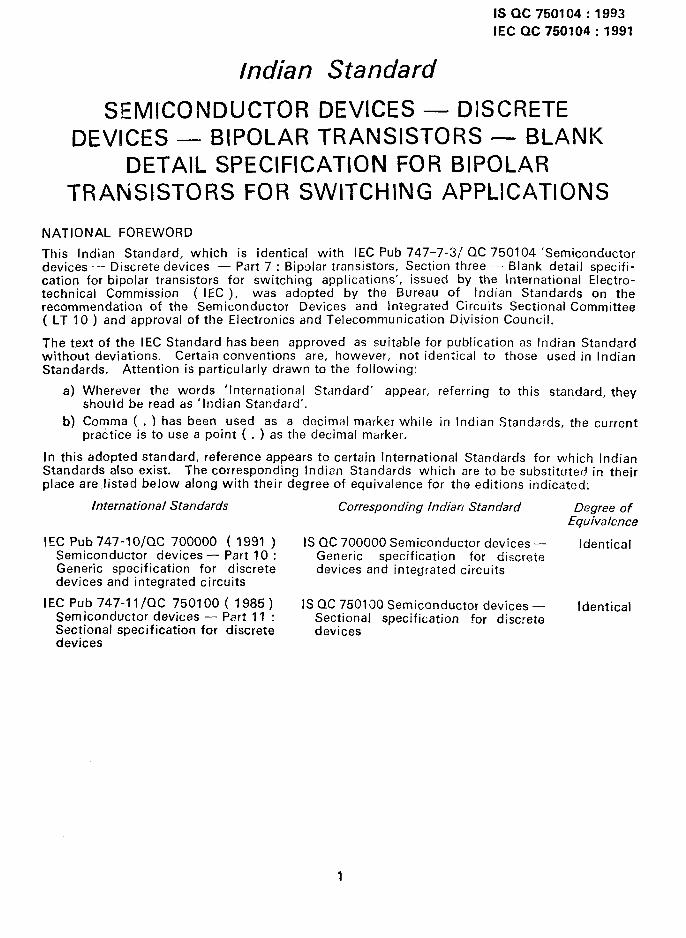
NATIONAL FOREWORD
This Indian Standard, which is identical with IEC Pub 747-7-31 QC 750104 ‘Semiconductor devices - Discrete devices - Part 7 : Bipolar transistors, Section three - Blank detail specifi- cation for bipolar transistors for switching applications’, issued by the international Electro- technical Commission ( IEC ), was adopted by the Bureau of Indian Standards on the recommendation of the Semiconductor Devices and Integrated Circuits Sectional Committee ( LT IO ) and approval of the Electronics and Telecommunication Division Council.
The text of the IEC Standard has been approved as suitable for publication as Indian Standard without deviations. Certain conventions are, however, not identical to those used in Indian Standards. Attention is particularly drawn to the following:
a) Wherever the words ‘International Stdndard’ appear, referring to this standard, they should be read as ‘Indian Standard’.
b) Comma ( , 1 has been used as a decimal marker while in Indian Standards, the current practice is to use a point ( . ) as the decimal marker.
In this adopted standard, reference appears to certain International Standards for which Indian Standards also exist. The corresponding Indian Standards which are to be substituted in their place are listed below along with their degree of equivalence for the editions indicated:
International Standards Corresponding Indian Standard Degree of Equivalence
IEC Pub 747-lO/QC 700000 ( 1991 ) IS QC 700000 Semiconductor devices - Identical Semiconductor devices - Part 10 : Generic specification for discrete Generic specification for discrete devices and integrated circuits devices and integrated circuits
IEC Pub 747-ll/QC 750100 ( 1985) IS QC 7501 JO Semiconductor devices - Semiconductor devices - Part 11 :
Identical
Sectional specification for discrete Sectional specification for discrete devices
devices
As in the Original Standard, this Page is Intentionally Left Blank
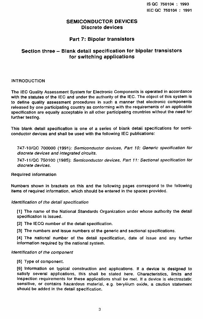
ISQC 750104 : 1993
IECQC 750104 : 1991
SEMICONDUCTOR DEVICES Discrete devices
Part 7: Bipolar transistors
Section three - Blank detail specification for bipolar transistors for switching applications
INTRODUCTION
The IEC Quality Assessment System for Electronic Components is operated in accordance with the statutes of the IEC and under the authority of the IEC. The object of this system is to define quality assessment procedures in such a manner that electronic components released by one participating country as conforming with the requirements of an applicable specification are equally acceptable in all other participating countries without the need for further testing.
This blank detail specification is one of a series of blank detail specifications for semi- conductoi devices and shall be used with the following IEC publications:
747;l O/QC 700000 (1991): Semiconductor devices, Part 10: Generic specification for discrete devices and integrated circuits.
747-l 1 IQC 750100 (1985): Semiconductor devices, Part 7 7: Sectional specification for discrete devices.
Required information
Numbers shown in brackets on this and the following pages correspond to the following items of required information, which should be entered in the spaces provided.
Idqtificafion of the detail specification
[l] The name of the National Standards Organization under whose authority the detail specification is issued.
[2] The IECQ number of the detail specification.
[3] The numbers and issue numbers of the generic and sectional specifications.
[4] The national number of the detail specification, date of issue and any further information required by the national system.
Identification of the component
[6] Type of component.
[S] Information on typical construction and applications. If a device is designed to satisfy several applications, this shall be stated here. Characteristics, limits and inspection requirements for these applications shall be met. If a device is electrostatic sensitive, or contains hazardous material, e.g. beryllium oxide, a caution statement should be added in the detail specification.
3
ISQC 750104 : 1993
IEC QC 750104 : 1991
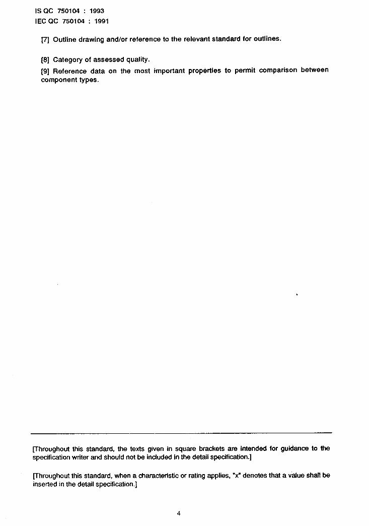
[7) Outline drawing and/or reference to the relevant standard for outlines.
[8] Category of assessed quality.
[9] Reference data on the most important properties to permit comparison between component types.
Fhroughout this standard, the texts given in square brackets are intended for guidance to the specification writer and should not be included in the detail specification.]
rhroughout this standard, when a characteristic or rating applies, “x” denotes that a value shall be inserted in the detail specification.]
4

ISQC 750104 : 1993
IEC QC 750104 : 1991
[Name (address) of responsible NAI 111 [Number of IECO detail specification 121 (and possibly of body from which specification plus issue number and/or date.]
is available).] QC 750104-xxx
ELECTRONIC COMPONENT OF ASSESSED I31 [National number of detail specification.] [41 QUALITY IN ACCORDANCE WITH: [This box need not be used if the National
Generic specification: Publication 747-IOlQC 700000 number repeats IECQ number.]
Sectional specification: Publication 747-l l/CC 750100
[and national references if different.]
DETAIL SPECIFICATION FOR: vype number(s) of the relevant device(s).]
I51
Ordering information: see clause 7 of this standard.
1 Mechanical description
Outline referendes:
IEC 191-2... [mandatory if available] and/or
national [if there is no IEC outline.]
171
2 Short description
Ambient or case-rated bipolar transistor for
switching applications, (NPNIPNP.]
Semiconductor material: [Si]
Encapsulation: [cavity or non-cavity.]
El
Outline drawing
[may be transferred to or given with more details in
clause 10 of this standard.]
Caution: Observe precautions for handling
ELECTROSTATIC SENSITIVE DEVICES
[if applicable]
Teminal identification
[drawing showing pin assignments including 3 Categories of assessed quality graphical symbols.]
[from subclause 2.6 of the generic
specification.] PI
Marking: [letters and figures, or colour code.] [The detail specification shall prescribe the information
to be marked on the device, if any.]
Reference data PI
[See subclause 2.5 of the generic specification
and/or clause 6 of this standard.]
[Polarity indication, if a special method is used.]
Information about manufacturers who ‘have components qualified to this detail specification is available in the current Gualified Products List.
5

-...
IS QC 750104 : 1993
IEC QC 750104 : 1991
4 Limiting values (absolute maximum rating system)
These values apply over the operating temperature range unless otherwise specified.
[Repeat only subclause numbers used, with title. Any additional values should be given at the appropriate place, but without subclause number(s).]
[Curves should preferably be given under clause 10 of this standard.]
Value Subclause Parameters Symbol
min. max.
4.1 Operating ambient or case temperatures T mblcare X X
4.2 Storage temperatures T l 18
X X
4.3 Collector-base voltage
Maximum continuous (direct) collector-base voltage
with zero emitter current
(should be given if VcER and/or VoEs are not given.
which are preferable) Vcao X
4.4 Collector-emitter voltage
One (preferably VcEo) or more of the following
shall be specified:
Maximum continuous (direct) collector-emitter voltage
with zero base current
V CEO X
Maximum continuous (direct) collector-emitter voltage
with specified reverse base voltage
Maximum continuous (direct) collector-emitter voltage
with base short-circuited to emitter
Maximum continuous (direct) collector-emitter voltage
with specified external resistance Ra.
V CEX
X
V CES
X
V CER
X
4.5 Emitter-base voltage:
Maximum emitter-base continuous (direct) reverse
voltage with zero collector current
V EBO X
4.6
4.7
Maximum continuous collector current and, where 42 X
appropriate, repetitive peak collector current I CM X
Where appropriate: maximum continuous base current; ‘a X
repetitive peak base current may be added I BM X
4.6 Where appropriate: maximum continuous emitter current; ‘E X
repetitive peak emitter current may be added I EM X
4.9
,4.9.1
4.9.2
Power dissipation:
Any special requirements for cooling or mounting should
be specified
Maximum total power dissipetion as’a function of. P,,,(T) X
temperature or:
Maximum virtual (equivalent) junction temperature, T(,1)
X
and maximum power dissipation P(tct) X
4.10 For case-rated types and, where appropriate, for ambient-rated types:
- area of safe operation (for example curves /, versus
VCE) d.c. and. where appropriate, pulse
6
ISQC 750104 : 1993
IECQC 750104 : 1991
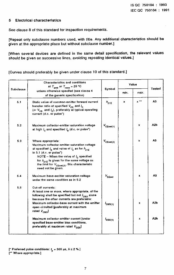
5 Electrical characteristics
See clause 8 of this standard for inspection requirements.
[Repeat only subclause numbers used, with title. Any additional characteristics should be given at the appropriate place but without subclause number.]
[When several devices are defined in the same detail specification, the relevant ValUSS
should be given on successive lines, avoiding repeating identical values.]
[Curves should preferably be given under clause 10 of this standard.]
Subclause
5.1
5.2
5.3
5.4
5.5
Characteristics and conditions
at Tmb or T,,,, = 25 ‘C
unless otherwise specifed (see clause 4
of the generic specification)
Static value of common-emitter forward current
transfer ratio at specified VCE and I,
(or Vc, and IE), preferably at typical operating
current (d.c. or pulse’)
Maximum collector-emitter saturation voltage
at high I, and specified /a (d.c. or pulse’)
Where appropriate: V CEsat(2)
Maximum collector-emitter saturation voltage
at specified /a and value of I, as for h2,E
in 5.1 (d.c. or pulse’)
NOTE - When the value of I, specified
for h21E is given for the same voltage as
the limit for VCEsalc2), this characteristic
need not be given.
Maximum base-emitter saturation voltage
under the same condition as in 5.2
Cut-off currents:
At least one or more, where appropriate, of the
following shall be specified but not lcao alone
because the other currents are preferable:
Maximum collector-base current with the emitter
open-circuited [preferably at maximum
rated Vceo]
Maximum collector-emitter current [under
specified base-emitter bias conditions,
preferably at maximum rated VCEX]
Symbol
h 21E
V CEsat(1)
V BEsat
I CBO(1)
I C=(l)
l- X
Value
max.
--
X l *
i Tested
A3
A2b
A3
A3
A2b
A2b
[’ Preferred pulse conditions: t p = 300 ps, 6 5 2 x.1
r* Where appropriate.]

ISQC 750104 : 1993
IEC QC 750104 : 1991
;ubclause
5.5
(cont.)
5.6
Characteristics and conditions
at Tmb or T,,,, = 25 “C
unless otherwise specified (see clause 4
of the generic specification)
Maximum collector-emitter current with specified
base-emitter resistance [preferably at maximum
rated VoER]
Maximum collector-emitter current with the base
short-circuited to the emitter [preferably at
maximum rated VcEs]
Maximum collector-emitter current with the base
open-circuited Ipreferably at maximum rated
‘CEO]
[and, when appropriate]
Maximum emitter-base current with the collector
open-circuited (preferably at maximum rated
VEBOl
Cut-off currents at high temperature:
[At least one, or more where appropriate, of the
following shall be specified but not /oeo alone
because the other currents are preferable]
Maximum collector-base current, at Vce
[preferably between 65 % and 85 % of maximum
rated Vceo], & = 0. and at a high temperature
Maximum collector-emitter current under specific
base-emitter bias conditions, at VC. [preferably
between 65 % and 65 % of maximum rated Vc,]
and at a high temperature
Maximum collector-emitter current with specified
base-emitter resistance, at V,., Ipreferably
between 65 46 and 35 96 of maximum rated V,,,]
and at a high temperature
Maximum collector-emitter current with the base
short-circuited to the emitter, at Vc, [preferably
between 65 % and 85 % of maximum rated VcCES]
and at a high temperature
Maximum collector-emitter current with the base
open-circuited, at Vc. [preferably between 65 %
and 85 96 of maximum rated VcEo] and at a high
temperature
Symbol
'cm(l)
‘Is(l)
I CEO(l)
I EBO
‘CBO(2)
Jcu((2)
‘m?(2)
I CES(2)
‘CEO(,)
T- Value
max.
Tested
A2b
A2b
A2b
A2b
C2b
C2b
C2b
C2b
C2b
a
ISQC 750104 : 1993
IEC QC 750104 : 1991
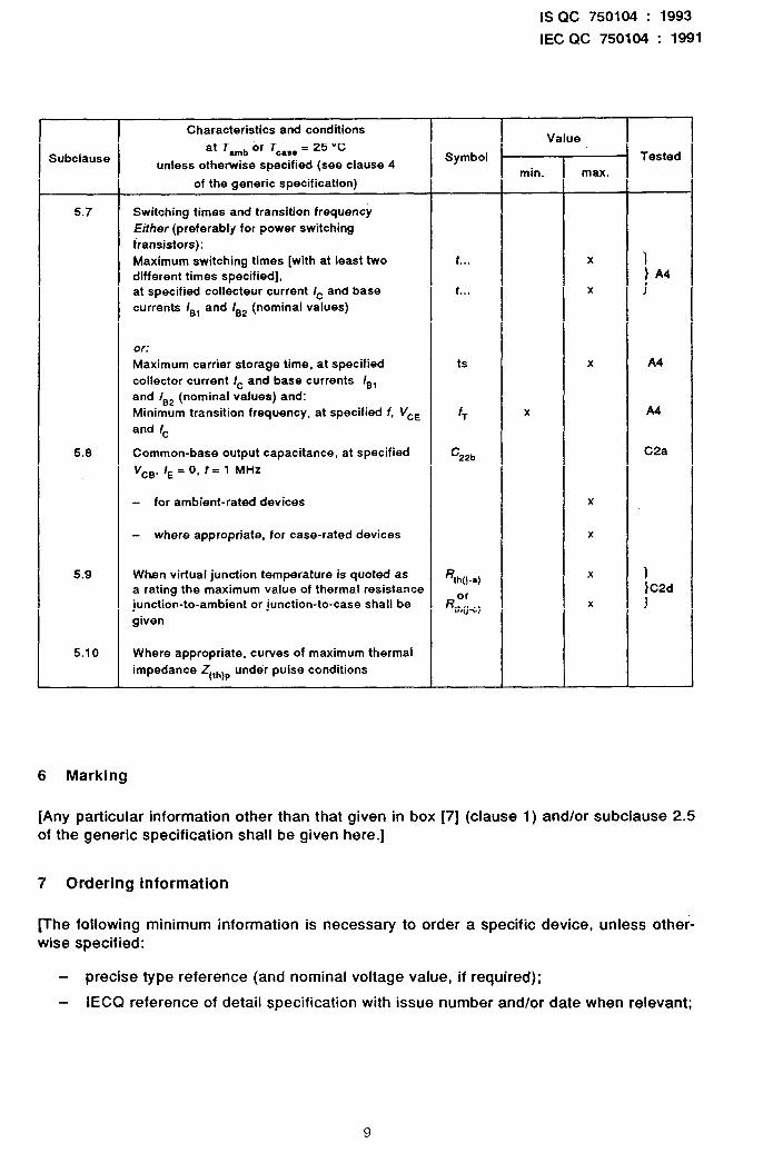
Subclause
5.7
5.8
5.9
5.10
Characteristics and conditions
at Tunb or T,,,, = 25 “C
unless otherwise specified (see clause 4
of the generic specification)
Switching times and transition frequency
Either (preferably for power switching
transistors):
Maximum switching times [with at least two different times specified], at specified collecteur current I, and base
currents la, and /as (nominal values)
or:
Maximum carrier storage time, at specified
collector current I, and base currents Is,
and /s2 (nominal values) and:
Minimum transition frequency, at specified f, Vcs
and Ic
Common-base output capacitance, at specified
V c., I, = 0, f- 1 MHz
- for ambient-rated devices
- where appropriate, for case-rated devices
When virtual junction temperature is quoted as a rating the maximum value of thermal resistance junction-to-ambient or junction-to-case shall be
given
Where appropriate, curves of maximum thermal
impedance ZnhjP under pulse conditions
T Symbol
t . . .
t 1..
ts
fr
C 22b
R WI-N
R or
rhU+
Value
X
max.
T Tested
1 1 A4 I
A4
A4
C2a
1 )C2d
1
6 Marking
[Any particular information other than that given in box [7] (clause 1) and/or subclause 2.5 of the generic specification shall be given here.]
7 Ordering information
[The following minimum information is necessary to order a specific device, unless other- wise specified:
- precise type reference (and nominal voltage value, if required);
- IECQ reference of detail specification with issue number and/or date when relevant;
9
IS QC 750104 : 1993 IEC QC 750104 : 1991
- category of assessed quality as defined in subclause 3.7 (clause 1 l’j of the sectional specification and, if required, screening sequence as defined in subclause 3.6 (clause 1 O*) of the sectional specification;
- any other particulars.]
8 Test conditions and inspection requirements
rhese are given in the following tables, where the values and exact test conditions to be used shall be specified as required for a given type, and as required by the relevant test in the relevant publication.]
[The choice between alternative tests or test methods shall be made when a detail specification is written.]
[When several devices are included in the same detail specification, the relevant conditions and/or values should be given on successive lines, where possible avoiding repetition of identical conditions and/or values.]
Throughout the following text, reference to subclause numbers is made with respect to the generic specification unless otherwise stated and test methods are quoted from clause 4 (clause 12’) of the sectional specification.
[For sampling requirements, either refer to, or reproduce, values of subclause 3.7 (clause 17 ‘;I of the sectional specification, according to applicable category(ies) of assessed quality.]
[For group A, the choice between AQL or LTPD system shall be made in the detail specification.]
__ __I_..__
.
Of future revision of IEC Publication 747-l 1.
IS QC 750104 : 1993
IEC QC 750104 : 1991
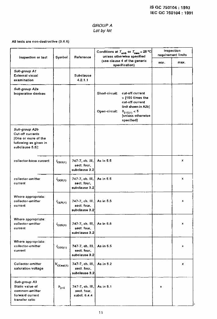
GROUP A Lot by lot
All tests are non-destructive (3.6.6)
Inspection or test
Subgroup A 7
External visual
examination
Subgroup A2a
Inoperative devices
Conditions at Tamr, or T,. = 25 *C Inspection
Symbol Reference unless otherwise specified requirement limits
(see clause 4 of the generic specification)
min. max.
Subclause
4.2.1 .l
Short-circuit: cut-off current
> IlOO times the
cut-off current
limit shown in A2b)
Open-circuit: It,,,(,) < 5
[unless otherwise
specified]
Subgroup A26
Cut-off currents
[One or more of the
following as given in
subclause 5.51:
collector-base current ‘NO(I) 747-7. ch. Ill, As in 5.5 X
sect. four,
subclause 3.2
collector-emitter
current ‘CEx(1) 747-7. ch. III, As in 5.5 X
sect. four,
subclause 3.2
Where appropriate:
collector-emitter
current
I CER(1)
747-7, ch. Ill, As in 5.5 X
sect. four,
subclause 3.2
Where appropriate:
collector-emitter I CES(1)
747-7, ch. Ill, As in 5.5 X
current sect. four,
subclause 3.2 ~_
Where appropriate:
collector-emitter ‘CEO(l)
747-7. ch. Ill, As in 5.5 X
current sect. four,
subclause 3.2
Collector-emitter
saturation voltage
V CEaaC(1)
747-7, ch. III, As in 5.2 X
sect. four,
subclause 3.2
Sub-group A3
Static value of
common-emitter
forward current
transfer ratio
h 21E
747-7, ch. Ill, As in 5.1 X
sect. four,
subcl. 6.4.4
11

ISQC 750104 : 1993
IEC QC 750104 : 1991
GROUP A (continued)
Inspection or test
Where appropriate:
collector-emitter
saturation voltage
Conditions at Ta.mb or 7,_ = 25 “C Inspection
Symbol Reference unless otherwise specified requirement limits
(see clause 4 of the generic specification)
min. max.
V CE42)
747-7, ch. III, As in 5.3 X
sect. four,
subclause 3.2
Base-emitter saturation VBEIPt 747-7, ch. III. As in 5.4 X
voltage sect. four.
subclause 3.2
Sub-group A4
Either:
switching times (at
least two values)
747-7, ch. Ill, Nominal values of lo, la, and la2
t . . . sect. four, VI = [specified] X
t . . . subclause 3.3 V2 = [specified] X
V cc = [specified]
RI” = [specified]
R = [specified]
Ini% maximum pulse transition
time = [specified]
or:
carrier storage time
and
transition frequency
747-7. ch. Ill. X
sect. four,
subclause 3.3
747-7. ch. III, VCE I [specified] X
sect. four, I, = [specified]
subclause 3.3 f = [specified]
12

IS QC 750104 : 1993
IEC QC 750104 : 1991 GROUP B
Lot by rot (in the case of category I, see the generic specification, subclause 2.6)
LSL = lower specification limit ] }
USL = upper specification limit j from group A
Only tests marked (D) are destructive (3.6.6)
Conditions at T_,,, or T,,, = 25 “C Inspection
unless otherwise specified requirement limits
Inspection or test Symbol Reference (see clause 4 of the generic
specification) min. max.
Sub-group B 1
Dimensions Subcl. 4.2.2. [See clause 1 of
appendix B this standard]
Sub-group 83
Bending, (D) if applicable 749, ch. II, Force = [see 749, ch. II, No damage
(dependent on subcl. 1.2 subclause 1.21
encapsulation)
Subgroup 84
Solderability 749, ch. II, [As specified] Good wetting
subcl. 2.1
Subgroup B5
Rapid change of 749. ch. Ill, [As specified]
temperature, clause 1
followed by
either:
- Damp heat cyclic (D) 749, ch. Ill, Test Db, variant 2.
(for non-cavity clause 4 severity = 55 “C,
devices) number of cycles =
with final measurements:
- cut-off current [Note] As in A2b USL
- forward current h 21 E 747-7, As in A3 LSL
transfer ratio ch. II,
subcl. 6.4.4
- saturation voltage
or:
Sealing (for cavity
devices)
Sub-group B8
Electrical endurance
(168 h)
V CE*at(l) 747-7, As in A2b USL
ch. III.
sect. four
subcl. 3.2
749, ch. Ill Subclauses 7.2, 7.3 or 7.4,
subcl. 7 combined with test Qc, 66-2-17
Relevant Operating life
747,... or
publication high temperature reverse bias
with final measurements:
- cut-off current NW As in A2b PUSL
- forward current h 21E 747-7. ch. II. As in A3 0.8LSL
transfer ratio subcl. 6.4.4
- saturation voltage V oEu,(,) 747-7. ch.lll. As in A2b 1 ,PUSL
sect. four,
subcl. 3.2
Subgroup CRRL Attributes information for 83. B4, B5 and 88.
[NOTE - Specify one cut-off current from sub-group A2b. preferably /,_ao.]
lj
IS QC 750104 :’ 1993
IEC QC 750104 : 1991
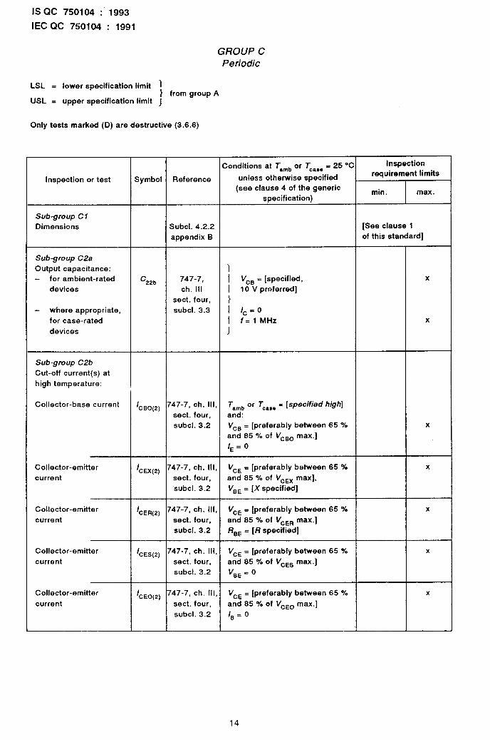
GROUP C Periodic
LSL = lower specification limit ]
USL = upper specification limit 1 from group *
Only tests marked (D) are destructive (3.6.6)
Inspection or test
Conditions at Tamb or T,,,, = 25 “C Inspection
Symbol Reference unless otherwise specified requirement limits
(see clause 4 of the generic min. max.
specification)
Subgroup Cl
Dimensions Subci. 4.2.2 [See clause 1
appendix B of this standard]
Subgroup C2a
Output capacitance: I - for ambient-rated C
22b 747-7. I Vce = [specified, X
devices ch. III I 10 V prnferred]
sect. four, 1 - where appropriate, subcl. 3.3 I ICE0
for case-rated 1 f=lMHz X
devices 1
Sub-group C2b
Cut-off current(s) at
high temperature:
Collector-base current ‘C,,(2)
747-7, ch. III. Tsmb or Tc_ = [specified high]
sect. four, and:
subcl. 3.2 Vce = [preferably between 65 % X
and 85 % of Vceo max.]
I, = 0
Collector-emitter
current
Collector-emitter
current
I CEX(2)
747-7. ch. Ill, VCE = [preferably between 65 % X
sect. four, and 85 % of Vcw max],
subcl. 3.2 Va8 = [X specified]
Collector-emitter
current
= [preferably between 65 46
Collector-emitter
current
14

ISQC 750104 : 1993
IECQC 750104 : 1991
GROUP C (continued)
inspection or test Symbol Reference
Conditions at Tarnb or 7,,_ = 25 % inspection
unles otherwise specified requirement limits
(see clause 4 of the generic specification)
min. max.
Sub-groups C2d
Thermal resistance,
where appropriate
Sub-group C3
Robustness of :
terminations
tensile and/or torque
(dependent on
encapsulation)
R ,h(,_*) 747-2, ch. IV (As specified] X
%J-C) subcl. 2.2
749, ch. II. [749. ch. II, subclause 1 .l or 1.41 No damage
subcl. 1.1
749, ch II,
subcl. 1.4
Sub-group C4
Resistance to soldering 749, ch. II, 1749, ch. II, subclause 2.21
heat (‘3 subcl. 2.2
with final measurements:
- cut-off current [Note] 747-7, ch. Ill. As in A2b USL
sect. four,
subcl. 3.2
- saturation voltage V CE,alc,j 747-7, ch. Ill, As in A2b USL
sect. four,
subcl. 3.2
- forward current h 21E
747-7. ch. II, As in A3 LSL
transfer ratio subcl. 6.4.4
Subgroup C6
Acceleration steady- 749, ch. II. [As specified]
state (for cavity devices clause 5
only)
with final measurements:
- cut-off current [Note] 747-7, ch. Ill. As in A2b
sect. four,
subcl. 3.2
- saturation voltage V CEw(1)
As in A2b
- forward current h21E
747-7. ch. II, As in A3
transfer ratio subcl. 6.4.4
[NOTE - Specify one cut-off current from subgroup A2b, preferably /oar,.]
15
IS QC 750104 : 1993 IEC,QC 750104 : 1991
GROUP C (continued)
Inspection or test Symbol Reference
Conditions at Tunb or 7,,, = 25 “C Inspection
unless otherwise specified requirement limits
(see clause 4 of the generic min. max.
specification)
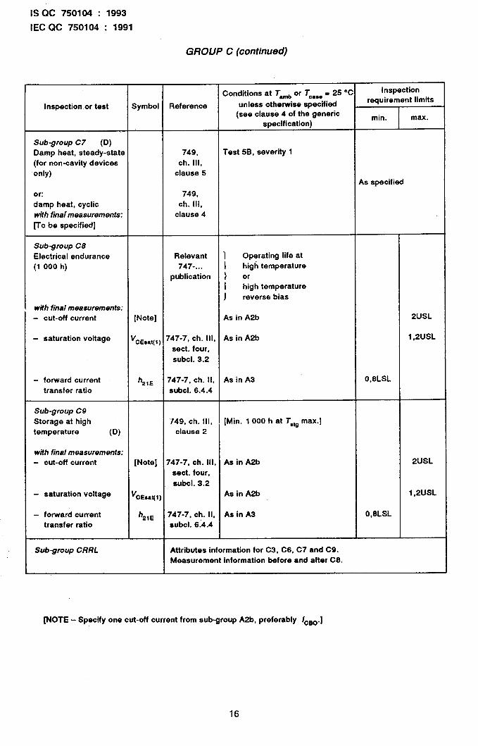
Subgroup C7 (0)
Damp heat, steady-state
(for non-cavity devices
only)
or:
damp heat, cyclic
with finalmeasurements:
(To be specified]
749,
ch. Ill,
clause 5
749,
ch. III,
clause 4
Test 58. severity 1
As specified
Subgroup CS
Electrical endurance Relevant 1 Operating life at
(1 000 h) 747-...
publication I
high temperature
1 t:gh temperature
J reverse bias
with final measurements:
- cd-off current [Note] As in A2b 2USL
- saturation voltage V ,.8,.r(,) 747-7, ch. Ill, As in A2b 1 .PUSL
sect. four,
subcl. 3.2
- forward current h 21E 747-7. ch. II, As in A3 0.8LSL
transfer ratio subcl. 6.4.4
Subgroup C9
Storage at high 749, ch. III. [Min. 1000 h at Tats max.]
temperature (D) clause 2
with final measurements:
- cut-off current [Note] 747-7, ch. Ill, As in A2b PUSL
sect. four,
subcl. 3.2
- saturation voltage V CEsat(l) As in A2b 1 .PUSL
- forward current h 21E 747-7. ch. II. As in A3 O,BLSL
transfer ratio subcl. 6.4.4
Subgroup CRRL Attributes information for C3. C6, C7 and C9.
Measurement information before and after C8.
WOTE - Specify one cut-off current from sub-group A2b, preferably /oeo.]
16

IS QC 750104 : 1993
IEC QC 750104 : 1991
9 Group D - Quattftcation approval tests
[When required, these tests shall be prescribed in the detail specification.]
10 Additional information (not for inspection purposes)
[To be given only as far as necessary for the specification and use of the device, for instance:
- temperature derating curves referred to in the limiting values;
- complete definition of a circuit for measurement, or of an additional method;
- detailed outline drawing.]
17