Is Now Part of - Power Management IC and Semiconductor ... · PDF fileTo learn more about ON...
20
To learn more about ON Semiconductor, please visit our website at www.onsemi.com Is Now Part of ON Semiconductor and the ON Semiconductor logo are trademarks of Semiconductor Components Industries, LLC dba ON Semiconductor or its subsidiaries in the United States and/or other countries. ON Semiconductor owns the rights to a number of patents, trademarks, copyrights, trade secrets, and other intellectual property. A listing of ON Semiconductor’s product/patent coverage may be accessed at www.onsemi.com/site/pdf/Patent-Marking.pdf. ON Semiconductor reserves the right to make changes without further notice to any products herein. ON Semiconductor makes no warranty, representation or guarantee regarding the suitability of its products for any particular purpose, nor does ON Semiconductor assume any liability arising out of the application or use of any product or circuit, and specifically disclaims any and all liability, including without limitation special, consequential or incidental damages. Buyer is responsible for its products and applications using ON Semiconductor products, including compliance with all laws, regulations and safety requirements or standards, regardless of any support or applications information provided by ON Semiconductor. “Typical” parameters which may be provided in ON Semiconductor data sheets and/or specifications can and do vary in different applications and actual performance may vary over time. All operating parameters, including “Typicals” must be validated for each customer application by customer’s technical experts. ON Semiconductor does not convey any license under its patent rights nor the rights of others. ON Semiconductor products are not designed, intended, or authorized for use as a critical component in life support systems or any FDA Class 3 medical devices or medical devices with a same or similar classification in a foreign jurisdiction or any devices intended for implantation in the human body. Should Buyer purchase or use ON Semiconductor products for any such unintended or unauthorized application, Buyer shall indemnify and hold ON Semiconductor and its officers, employees, subsidiaries, affiliates, and distributors harmless against all claims, costs, damages, and expenses, and reasonable attorney fees arising out of, directly or indirectly, any claim of personal injury or death associated with such unintended or unauthorized use, even if such claim alleges that ON Semiconductor was negligent regarding the design or manufacture of the part. ON Semiconductor is an Equal Opportunity/Affirmative Action Employer. This literature is subject to all applicable copyright laws and is not for resale in any manner.
Transcript of Is Now Part of - Power Management IC and Semiconductor ... · PDF fileTo learn more about ON...

To learn more about ON Semiconductor, please visit our website at www.onsemi.com
Is Now Part of
ON Semiconductor and the ON Semiconductor logo are trademarks of Semiconductor Components Industries, LLC dba ON Semiconductor or its subsidiaries in the United States and/or other countries. ON Semiconductor owns the rights to a number of patents, trademarks, copyrights, trade secrets, and other intellectual property. A listing of ON Semiconductor’s product/patent coverage may be accessed at www.onsemi.com/site/pdf/Patent-Marking.pdf. ON Semiconductor reserves the right to make changes without further notice to any products herein. ON Semiconductor makes no warranty, representation or guarantee regarding the suitability of its products for any particular purpose, nor does ON Semiconductor assume any liability arising out of the application or use of any product or circuit, and specifically disclaims any and all liability, including without limitation special, consequential or incidental damages. Buyer is responsible for its products and applications using ON Semiconductor products, including compliance with all laws, regulations and safety requirements or standards, regardless of any support or applications information provided by ON Semiconductor. “Typical” parameters which may be provided in ON Semiconductor data sheets and/or specifications can and do vary in different applications and actual performance may vary over time. All operating parameters, including “Typicals” must be validated for each customer application by customer’s technical experts. ON Semiconductor does not convey any license under its patent rights nor the rights of others. ON Semiconductor products are not designed, intended, or authorized for use as a critical component in life support systems or any FDA Class 3 medical devices or medical devices with a same or similar classification in a foreign jurisdiction or any devices intended for implantation in the human body. Should Buyer purchase or use ON Semiconductor products for any such unintended or unauthorized application, Buyer shall indemnify and hold ON Semiconductor and its officers, employees, subsidiaries, affiliates, and distributors harmless against all claims, costs, damages, and expenses, and reasonable attorney fees arising out of, directly or indirectly, any claim of personal injury or death associated with such unintended or unauthorized use, even if such claim alleges that ON Semiconductor was negligent regarding the design or manufacture of the part. ON Semiconductor is an Equal Opportunity/Affirmative Action Employer. This literature is subject to all applicable copyright laws and is not for resale in any manner.

www.fairchildsemi.com
© 2001 Fairchild Semiconductor Corporation www.fairchildsemi.com Rev. 1.1 • 5/5/16
AN-9016 IGBT Basics
Table of Contents
1. Introduction ......................................................................................................................................... 2
2. Device Structure and Operation .......................................................................................................... 2
2.1 Structure ....................................................................................................................................... 2
2.2 Operation ...................................................................................................................................... 3
3. Basic Characteristics ............................................................................................................................ 3
3.1 Advantages, Disadvantages and Characteristic Comparison with BJT and MOSFET ................ 3
3.2 Latch-Up....................................................................................................................................... 4
3.3 Static Blocking Characteristics .................................................................................................... 5
3.4 Leakage Current ........................................................................................................................... 5
3.5 Forward Conduction Characteristics ............................................................................................ 5
3.6 Switching Characteristics ............................................................................................................. 7
3.7 SOA (Safe-Operating-Area) ......................................................................................................... 8
4. Explanation of Data Sheet Parameters .............................................................................................. 10
4.1 Absolute Maximum Ratings....................................................................................................... 10
4.2 Thermal Characteristics.............................................................................................................. 10
4.3 Electrical Characteristics of the IGBT ....................................................................................... 12
4.4 Electrical Characteristics of a DIODE ....................................................................................... 16

AN-9016 APPLICATION NOTE
© 2001 Fairchild Semiconductor Corporation www.fairchildsemi.com Rev. 1.1 • 5/5/16 2
1. Introduction
Prior to the development of the IGBTs (insulated gate
bipolar transistor), power MOSFETs were used in medium
or low voltage applications which require fast switching.
Whereas bipolar power transistors, thyristors and GTOs
were used in medium to high voltage applications, which
require high current conduction. A power MOSFET allows
for simple gate control circuit design and has excellent fast
switching capability. On the other hand, at 200 V or higher,
it has the disadvantage of rapidly increasing on-resistance as
the breakdown voltage increases. The bipolar power
transistor has excellent on-state characteristics due to the
low forward voltage drop, but its base control circuit is
complex, and fast switching operation is difficult as com-
pared with the MOSFET. The IGBT developed in the early
1980s has the combined advantages of the above two
devices. It has a MOS gate input structure, which has a
simple gate control circuit design and is capable of fast
switching up to 100kHz. Additionally, because the IGBT
output has a bipolar transistor structure, its current
conduction capability is superior to a bipolar power
transistor. Based upon these excellent characteristics, the
IGBT has been extensively used in applications exceeding
300V voltage as an alternative to power MOSFETs and
bipolar power transistors. Its area of application continues to
increase. The IGBT is becoming more modular as its use
increases in applications that require higher current
conduction capability.
History of the Fairchild IGBT
Fairchild Semiconductor began developing the IGBT in
1992. This was later than its competitors for a power
semiconductor company. However, Fairchild
Semiconductor was able to catch up with its leading
competitors with the development of the third generation
600 V IGBT and 1500 V ultra-fast IGBT for 220 V power
IH applications in 1995. In 1996, Fairchild Semiconductor
developed the 600 V rugged type RUF series with its own
stripe pattern. This has strengthened short circuit
withstanding capability, which makes it suitable for motor
control applications such as inverters. Following this
development, Fairchild Semiconductor used trench
technology in 1998 to develop the 400 V IGBT for camera
strobes and the 900 V IGBT for 110 V power IH
applications. Both of these require low-loss high current
conduction capabilities. These design achievements
indicated that Fairchild Semiconductor now possessed both
planar and trench technologies. In particular, Fairchild has
achieved world-class quality in 1998 by developing 1200 V
IGBT using SDB (silicon direct bonding) technology.
Fairchild began research on SDB in 1996. Unlike existing
technology, which uses an epi-grown wafer, SDB
technology binds P+ substrate and N- substrate directly to
allow easier manipulation of the thickness of the N-
substrate. This enables easier fabrication of high voltage
IGBTs. Specifically, as the formation of a high density N+
buffer layer is possible, fast switching characteristics can be
obtained without high density electron irradiation, which
increases the leakage current and decreases reliability.
Hence, it enables the production of high speed, highly
efficient and reliable IGBTs. It is also suitable for large
capacity drives, as it has the same temperature
characteristics as the NPT IGBT, which is suitable for a
parallel drive. In the year 2000, Fairchild has applied this
technology to develop 1500 V and 1700 V IGBTs. These
can be used in 220 V 1 φ IH applications. Now, Fairchild is
in the process of developing IPMs (Intelligent Power
Modules), which are IGBT Inverter Modules that combine
the control ICs in order to provide a lot of intelligent
functions. The IPMs will drastically change the three-phase
AC/DC Motor Speed Control arenas paving the way for
reliable, compact and high performance designs.
2. Device Structure and Operation
2.1 Structure
The IGBT combines the advantages of a power MOSFET
and a bipolar power transistor. Similarly its structure is a
combination of the two devices. As shown in Figure 1, the
input has a MOS gate structure, and the output is a wide
base PNP transistor. The base drive current for the PNP
transistor is fed through the input channel. Besides the PNP
transistor, there is an NPN transistor, which is designed to
be inactivated by shorting the base and the emitter to the
MOSFET source metal. The 4 layers of PNPN, which
comprises the PNP transistor and the NPN transistor, form a
thyristor structure, which causes the possibility of a latch-
up. Unlike the power MOSFET, it does not have an integral
reverse diode that exists parasitically, and because of this it
needs to be connected with the appropriate fast recovery
diode when needed.
Figure 1. Equivalent Circuit for the IGBT and a Cross
Section of the IGBT Structure (PT and N-Channel)

AN-9016 APPLICATION NOTE
© 2001 Fairchild Semiconductor Corporation www.fairchildsemi.com Rev. 1.1 • 5/5/16 3
PT and NPT
An IGBT is called a PT (punch-through) or asymmetrical
when there is an N+ buffer layer between the P+ substrate
and N- drift region. Otherwise, it is called an NPT (non-
punch-through) IGBT or symmetrical IGBT. The N+ buffer
layer improves turn-off speed by reducing the minority
carrier injection quantity and by raising the recombination
rate during the switching transition. In addition, latch-up
characteristics are also improved by reducing the current
gain of the PNP transistor. The problem is that the on-state
voltage drop increases. However, the thickness of the N-
drift region can be reduced with the same forward voltage
blocking capability because the N+ buffer layer improves
the forward voltage blocking capability. As a result, on-state
voltage drop can be lowered. Hence, the PT-IGBT has
superior trade-off characteristics as compared to the NPT-
IGBT in switching speed and forward voltage drop.
Currently, most commercialized IGBTs (Fairchild IGBTs)
are PT-IGBTs. Section 3.3 about static blocking
characteristics illustrates that IGBT forward and reverse
blocking capability are approximately equal because both
are determined by the same N- drift layer thickness and
resistance. The reverse-blocking voltage of PT-IGBTs that
contain N+ buffer layer between P+ substrate and N- drift
region is lowered to tens of volts due to the existence of a
heavy doping region on both sides of J1.
2.2 Operation
Turn-On
When the device is in the forward blocking mode, and if the
positive gate bias (threshold volt-age), which is enough to
invert the surface of P-base region under the gate, is applied,
then an n-type channel forms and current begins to flow. At
this time the anode-cathode voltage must be above 0.7 V
(potential barrier) so that it can forward bias the P+
substrate / N- drift junction (J1). The electron current, which
flows from the N+ emitter via the channel to the N- drift
region, is the base drive current of the vertical PNP
transistor. It induces the injection of hole current from the
P+ region to the N- base region. The conductivity
modulation improves because of this high level injection of
the minority carrier (hole). This increases the conductivity
of the drift region by a factor varying from ten to hundred.
This conductivity modulation enables IGBTs to be used in
high voltage applications by significantly reducing the drift
region resistance. There are two kinds of currents flowing
into the emitter electrode. One is the electron current (MOS
current) flowing through the channel, and the other is the
hole current (bipolar current) flowing through the P+ body /
N- drift junction (J2).
Turn-On
The gate must be shorted to the emitter or a negative bias
must be applied to the gate. When the gate voltage falls
below the threshold voltage, the inversion layer cannot be
maintained, and the supply of electrons into the N- drift
region is blocked, at which point, the turn-off process
begins. However, the turn-off cannot be quickly completed
due to the high concentration minority carrier injected into
the N- drift region during forward conduction. First, the
collector current rapidly decreases due to the termination of
the electron current through the channel, and then the
collector current gradually reduces, as the minority carrier
density decays due to recombination.
3. Basic Characteristics 3.1 Advantages, Disadvantages and
Characteristic Comparison with BJT and MOSFET
Advantages
(1) High Forward conduction current density and low on-
state voltage drop: The IGBT has a very low on-state
voltage drop due to conductivity modulation and has
superior on-state current density compared to the power
MOSFET and bipolar transistor. So a smaller chip size
is possible and the cost can be reduced.
(2) Low driving power and a simple drive circuit due to the
input MOS gate structure: The IGBT can easily be
controlled as compared to current controlled devices
(thyristor, BJT) in high voltage and high current
applications.
(3) Wide SOA: With respect to output characteristics, the
IGBT has superior current conduction capability
compared with the bipolar transistor. It also has
excellent forward and reverse blocking capabilities.
Disadvantages
(1) Switching speed (less than 100 kHz) is inferior to that
of the power MOSFETs, but it is superior to that of the
BJT. The collector current tailing due to the minority
carrier causes he turn-off speed to be slow.
(2) There is the possibility of latch-up due to the internal
PNPN thyristor structure.
The Characteristics Comparison with a BJT and a MOSFET
Table 1. The IGBT Characteristics Comparison with BJT, MOSFET
Features BJT MOSFET IGBT
Drive Method Current Voltage Voltage
Drive Circuit Complex Simple Simple
Input Impedance Low High High
Drive Power High Low Low
Switching Speed Slow (µS) Fast (nS) Middle
Operating Frequency
Low (< 100kHz)
Fast (< 1MHz)
Middle
S.O.A Narrow Wide Wide
Saturation Voltage
Low High Low

AN-9016 APPLICATION NOTE
© 2001 Fairchild Semiconductor Corporation www.fairchildsemi.com Rev. 1.1 • 5/5/16 4
3.2 Latch-Up
The IGBT contains a parasitic PNPN thyristor structure
between the collector and the emitter. A latch-up means the
turning on of the thyristor. When there is action by a
thyristor, the IGBT current is no longer controlled by the
MOS gate. The IGBT would be destroyed because of
excessive power dissipation produced by the amount of
current over the rated value between the collector and the
emitter.
Causes of latch-up
Static latch-up mode: Since the conductivity of the drift
region under the gate electrode is increased by the
introduction of electron current through the channel, most of
the holes injected into the drift region are injected at the P
body region under the channel and flow to the source metal
along the bottom of N+ source. Due to this, the lateral
voltage drops across the shunting resistance (RS, refer to
Figure 1) of the P body layer. If this voltage drop becomes
greater than the potential barrier of the N+ source / P body
layer junction (J3), electrons are injected from the N+
source to the P body layer, and the parasitic NPN transistor
(N+ source, P body and N- drift) is turned-on. If the sum of
the two NPN, PNP parasitic transistors’ current gain
becomes 1(αNPN + αPNP ≥ 1), latch-up occurs.
Dynamic latch-up mode: When the IGBT is switched off,
the depletion layer of the N- drift / P body junction (J2) is
abruptly extended, and the IGBT latches up at a current
lower than 1/2 of the static latch-up current due to the
displacement current. And because of this, the safe
operating area is limited.
Avoidance of latch-up
The first method is to prevent the NPN parasitic transistor
from turning on, and the second is to keep the sum of the
two NPN, PNP parasitic transistors’ current gain less than 1
(αNPN + αPNP<1) when the NPN parasitic transistor is turned
on. In the latter case, the two transistors’ current gain must
be reduced. As the current gain is proportional to the base
transport factor and the injection efficiency of an emitter-
base junction, both must be reduced. In the PNP transistor,
electron irradiation and the inserting of a N+ buffer layer
between the P+ substrate and N- drift region can be used,
but it is difficult to reduce the current gain in the NPN
transistor. So the following representative methods to
improve latch-up characteristics are focused on pre-venting
the turn-on of the NPN parasitic transistor.
(1) Application of P+ Body
This method is applied to most MOS gate power devices. In
addition to the body, a highly doped P+ region is formed in
the middle of the body, and it covers most of the bottom
part of source. When the doping concentration of the P+
region is excessively raised to improve latch-up
characteristics, the P+ region affects the threshold voltage
by diffusing the channel region and debasing the forward
characteristics.
(2) Cushion Structure p+ Double Implantation:
When using a highly doped P+ body, there are limitations in
lowering the resistance of the bottom part of N+ source as
the doping concentration of the P+ body reduces
horizontally due to diffusion. Ion is first injected to form the
N+ source. Then high energy p+ ion is injected, and it is put
through a thermal process to form P+ region at the bottom
of the N+ source. Fairchild is producing latch-up proofed
IGBTs by applying this method and EBR (Emitter Ballast
Resistor: further explained in (6)).
(3) Application of short N+ source:
This method reduces the resistance at the bottom of the N+
source.
(4) Reduction of the hold current:
The voltage drop across the bottom of the N+ source can be
reduced by reducing the hole current passing through the P
body. Inserting the highly doped N+ buffer, reducing the
space between P bodies, and reducing the current gain by
electron irradiation are the methods to reduce the hole
current.
(5) Minority Carrier By-Pass:
The minority carrier by-pass design has two hole current
paths. One is a normal path and the other flows to the
emitter contact directly without passing through the bottom
of the N+ emitter. So the hole current flowing through the
bottom of the N+ emitter is reduced to half, and the latching
current density doubles. In spite of an increase in the on-
state voltage drop, this method is widely used because it
enables safe operation without latch-up phenomenon at
higher current and temperature.
(6) Layout:
The latch-up characteristics can be improved by changing
the N+ source’s cell structure on the surface of the device.
Generally, a linearly structured cell has worse forward
current conduction characteristics than a cellularly
structured cell, but shows better latch-up characteristics. A
MSS (multiple surface short) structure with better latch-up
characteristics as compared to the linear structure has also
been developed. There is another method (EBR) used in
Fairchild IGBTs, which increases the voltage drop level
across the bottom of N+ source that forward biases the
emitter (N+ source region)-base (P body region) junction
(J3). This is done by making the voltage drop inside the N+
source by changing the length of the N+ source.
(7) Others:
There is also a method to build in a sense IGBT cell and
protection devices. This limits the current by reducing the
gate voltage automatically, when the current flows over a
certain limit. If a large series gate resistance RG is used
when the IGBT is applied to a certain set, the turn-off speed
is slowed and the diffusion speed of the depletion region of
the drift region also slows down. Hence, the dynamic latch-

AN-9016 APPLICATION NOTE
© 2001 Fairchild Semiconductor Corporation www.fairchildsemi.com Rev. 1.1 • 5/5/16 5
up can be prevented. IGBTs currently under production
have the latch-up proof characteristics.
High Temperature characteristics (latching current density)
With a rise in temperature, the current gains of the NPN and
PNP transistors increase. This decreases the latching
current. The effect is aggravated by an increase in the
resistance of the P base region due to a decrease in hole
mobility.
3.3 Static Blocking Characteristics
Reverse Blocking Capability
When negative voltage is introduced to the collector as
shown in Figure 1, the P+ substrate / N-drift junction (J1) is
reverse biased, and the depletion layer generally expands to
the N- drift region. As such, securing an optimal design in
resistivity and thickness for the N- drift region is essential in
obtaining desirable reverse blocking capability. As a general
guideline, the width of the N-drift region is equivalent to the
sum of depletion width at maximum operating voltage and
minority carrier diffusion length. It is important to optimize
the breakdown voltage while maintaining a narrow N- drift
region width, as the forward voltage drop increases with an
increase in N- drift region width. The following is an
equation for calculating the N- drift region width:
Where, d1: N-drift region width
Vm: maximum blocking voltage
ND: doping concentration
Lp: minority carrier diffusion length
Forward Blocking Capability
When the gate is shorted at the emitter, and a positive
voltage is introduced at the collector; the P base / N- drift
region junction (J2) is reverse biased, and it is supported up
to the rated voltage by the depletion region formed at the N-
drift region.
3.4 Leakage Current
Leakage current is divided into two types. One is leakage
current from the depleted drift region, and the other flows
on the surface of the junction termination. Since the IGBT
uses a P+ substrate and is irradiated with electrons to
improve switching speed, the amount of leak-age current
from the drift region is greater than that of the power
MOSFET. If there is a high voltage between the anode and
cathode when the IGBT is off, the depletion region widens
to nearly the entire drift region from the P+ body / N- drift
junction (J2), and the entire region becomes depleted. The
electron hole created by the heat of the depletion region is
manifested as leakage current according to the area of the
depletion region and minority carrier lifetime. This
increases with the increase of the rated voltage and current.
In particular, the leakage current increase as the minority
carrier lifetime shortens. As such, leakage current tends to
increase with higher speed IGBTs.
3.5 Forward Conduction Characteristics
Due to its structure, the IGBT is sometimes viewed as a
serial connection of the MOSFET and PiN diode, and
sometimes it is seen as a wide base PNP transistor driven by
the MOSFET in Darlington configuration. The former
description can be used to understand the behavior of the
device, but the latter better describes the IGBT.
Figure 2. Static Characteristics of the IGBT
Figure 2 is a graph of the IGBT’s static characteristics. Even
if a MOSFET channel of the input side is formed, the
collector current does not flow if the anode-cathode forward
voltage drop does not exceed approximately 0.7 V as in the
PiN diode. In addition, the current is saturated when the
voltage across the MOSFET channel is greater than (VGE –
Vth) and has an infinite output resistance, as in a power
MOSFET. However, in a symmetrical IGBT, the collector
cur-rent increases with the increase in collector voltage, and
the rate of increase in the collector current also increases
with the increase in collector voltage. Such finite output
resistance is due to a shortening of the channel due to an
increase in the collector voltage, and a secondary decrease
in the drain output resistance due to bipolar transistor
current flow. In order to increase the collector output
resistance, an asymmetrical structure with a N+ buffer layer
between the N- drift region and P+ substrate is used to
prevent an increase in the bipolar transistor’s current gain
with the increase in the collector voltage. In an
asymmetrical structure, the width of the un-depleted N- drift
region does not change rapidly with the increase in the
collector voltage due to the high concentration of the buffer
layer, but it remains the same width as the N+ buffer layer
for all collector voltages. This results in a constant value of
the PNP transistor’s current gain. In addition to this, the N+
buffer layer reduces the injection efficiency of the P+
substrate / N+ buffer junction (J1). This reduces the current
gain of the PNP transistor. As such, an IGBT with an
asymmetrical structure has much superior output

AN-9016 APPLICATION NOTE
© 2001 Fairchild Semiconductor Corporation www.fairchildsemi.com Rev. 1.1 • 5/5/16 6
characteristics than a symmetrical type. In addition,
collector output resistance can be increased with electron
irradiation to shorten the minority carrier lifetime, which
reduces the diffusion length. The following is the equation
for obtaining the saturated collector current of the IGBT:
Where, µns: surface mobility of electrons
Cox: gate-oxide capacitance per unit area
Z: channel width
LCH: channel diffusion length
Vth: threshold voltage
VGE: applied gate voltage
Transconductance at the active region can be obtained by
differentiating the IC,sat with respect to VGE.
The IGBT’s saturated collector current and
transconductance are higher than those of the power
MOSFETs of the same aspect ratio (Z/LCH). This is
because the PNP transistor’s cur-rent gain (αPNP) is less
than 1 (0.2 to 0.3 in general).
On-state voltage drop
Forward current-voltage characteristics and the conduction
loss of a MOSFET are described as on-resistance. On the
other hand, the characteristics of the IGBT are described as
voltage drop at rated current, as is the case with the bipolar
power transistor. On-state voltage drop is comprised of
voltage drop of the forward biased P+ substrate / N- drift
junction (J1), the voltage drop of conductivity modulated N-
drift region and the voltage drop of MOSFET. Cut-in
voltage for forward biased J1 is about 0.7 V at room
temperature. Cut-in voltage decreases due to a sharp
increase in intrinsic carrier concentration as the temperature
rises. The voltage drop of the N drift region can be obtained
by integrating the electric field of the entire drift region, and
it is generally less than 0.1 V due to a strong conductivity
modulation caused by injected holes from J1. The voltage
drop of a MOSFET is the sum of the voltage drops from the
channel region, JFET region and accumulation layer. Due to
a decrease in drift layer resistance, the portion of JFET
resistance and channel resistance is increased in the voltage
drop between on-state collector-emitter. Hence, low JFET
and channel resistance design are important factors in
obtaining the best performance in an IGBT. The voltage
drop at the channel is proportional to the channel length,
gate oxide thickness. And it is inversely proportional to
channel width, electron mobility and gate bias. The channel
width can be increased by increasing the concentration of
circuits by decreasing the size of each unit cell. But because
of this the JFET resistance increases significantly, so the
optimal size of the unit cell exists for each voltage rat-ing.
The IGBT decreases the minority carrier lifetime with
electron irradiation in order to improve the switching speed,
and this increases the on-state voltage drop. Even in IGBTs
with the same structure, the IGBT with a fast switching
speed has a larger voltage drop, and the IGBT with a slower
switching speed has a smaller on-state voltage drop
depending on the condition of electron irradiation, which
takes place after device fabrication.
High Temperature characteristics
One must be aware of the changes in characteristics from
changes in temperature, as the IGBT’s input characteristics
are similar to a MOSFET, and output characteristics are
similar to bipolar transistors. As temperature rises, the
energy barrier of the P+ substrate / N- drift region junction
(J1: emitter-base junction of PNP transistor) decreases,
which leads to a lower cut-in voltage, and the threshold
voltage decreases as in a MOSFET. As channel resistance
increases, the amount of electron current (MOS current)
decreases, which is injected to the N-drift region. However,
current gain, which is the ratio of the hole current (bipolar
current) to the electron current, increases. In addition, N-
drift region (base of the PNP transistor) resistance increases.
Due to these characteristics, changes in cut-in voltage of J1
are larger than those in channel resistance and N- drift
region resistance at low collector current level, so the IGBT
has negative temperature coefficient similar to the bipolar
transistor. On the other hand, channel resistance and N- drift
region resistance determine the on-state voltage at high
collector current, which results in a positive temperature
coefficient similar to a power MOSFET. The cross-over
point for the two characteristics is different for each
product, and the collector-emitter voltage drop is
independent from temperature at the crossover point. In real
applications, it is used in areas with negative temperature
coefficient, and these factors must be considered in parallel
application. Figure 3-to-Figure 5 illustrate these
characteristics with graphs from the data sheet.
Figure 3. Typical Saturation Voltage Characteristics

AN-9016 APPLICATION NOTE
© 2001 Fairchild Semiconductor Corporation www.fairchildsemi.com Rev. 1.1 • 5/5/16 7
Figure 4. Saturation Voltage vs. Case Temperature at
variant Current Level
Figure 5. Saturation Voltage vs. VGE due to Collector
Current, Case Temperature
3.6 Switching Characteristics
Turn-on
When the device is in the forward blocking mode, and if the
positive gate bias (threshold voltage), which is enough to
invert the surface of P base region under the gate, is applied,
then an n-type channel forms and the current begins to flow.
At this time the anode-cathode voltage must be above 0.7 V
(potential barrier), so that it can forward bias the P+
substrate / N- drift junction (J1). The electron current
flowing from the N+ emitter to the N- drift region through
the channel is the base drive current of the vertical PNP
transistor, and it induces a minority carrier (hole) injection
from the P+ region to the N- base region. The current that
flows to the emitter electrode are divided into the electron
current (MOS current) flowing through the channel and
bipolar current flowing through the P body / N- drift
junction (J2). When gate bias falls to near the threshold
voltage at on-state, the inversion layer conductivity is
reduced, and significant voltage drop that arises from
electron current flow occurs across the region as in a
MOSFET. When the voltage drop is equal to the difference
between the gate bias and threshold voltage (VGE - Vth),
then the channel is pinched off. At this point, the electron
current becomes saturated. Since this limits the base drive
current of the PNP transistor, the hole current flowing
through the PNP transistor is also limited. As a result, the
device operates with saturated cur-rent at the active region
(gate controlled output current).
Turn-off
The gate must be shorted to the emitter or a negative bias
must be applied to the gate. When the gate voltage falls
below the threshold voltage, the inversion layer cannot be
maintained, and the supply of electrons into the N- drift
region is blocked. At this point the turn-off process begins.
As illustrated in Figure 6, the collector current (ICO) falls to
zero in two stages. As the electron current supplied through
the MOSFET channel during the on-state is stopped,
collector current suffers an initial abrupt fall (ICD). After
that, the tail current (ICT) comes from the minority carrier
(hole) that was injected through the N- drift region from the
P+ substrate during the on-state. The tail current of the
IGBT lowers switching characteristics and increases
switching loss. Since N- drift region is the base of the PNP
transistor, it cannot be approached from outside, so it is not
possible to control the tail current from outside. But it can
be con-trolled with the amount of minority carrier (hole)
injected through the N- drift region and recombination rate
when it is off. In order to reduce the amount of injected
minority carrier and increase the recombination rate when it
is off, the concentration and the thickness of the N+ buffer
layer between the P+ substrate and N- drift region must
increase, as well as the dose of electron irradiation (in FSC,
electron irradiation is applied to above 600 V class except
400 V) that takes place after device fabrication. However,
improving the switching speed of the IGBT generally
accompanies reduced current handling capability. As such,
the trade-off between switching speed, which is related to

AN-9016 APPLICATION NOTE
© 2001 Fairchild Semiconductor Corporation www.fairchildsemi.com Rev. 1.1 • 5/5/16 8
switching loss, and forward voltage drop, which in turn is
related to conduction loss, is important. The asymmetric
structure is superior in such trade-offs as compared to a
symmetric structure, and it can be improved by increasing
the doping concentration in the buffer layer. In terms of
power loss, the power MOSFET is better suited for lower
blocking voltage and high operating frequency applications,
while the IGBT is better suited for higher blocking voltage
and lower operating frequency.
Figure 6. Collector Current during Turn-off
High Temperature characteristics
The minority carrier lifetime in the drift region increases as
the temperature increases. This not only delays
recombination process (tail current) of the minority carrier,
but it also increases the PNP transistor gain. So the portion
of the initial abrupt fall (ICD) in the overall collector current
reduces. As such, tF (fall time) of the spec is lengthened, and
turn-off time increases with an increase in temperature, and
the asymmetric structure has a lower rate of increase than
the symmetric structure.
3.7 SOA (Safe-Operating-Area)
The SOA of an IGBT can be divided into the following
three boundaries based on the stress conditions of voltage
and current.
(1) High voltage, low current: Maximum voltage is
limited by breakdown voltage.
(2) High current, low voltage: Maximum current is
limited by latch-up of parasitic thyristor.
(3) Simultaneous high current and voltage: Limited by
the rise in temperature caused by high power
dissipation.
If the high current and voltage are introduced
simultaneously for a short time, then the SOA is no longer
limited by power dissipation. The following explanation
illustrates the safe operating area for short duration
simultaneous application of high current and voltage stress
at the time of turn-on and turn-off of the IGBT with
inductive load with FBSOA and RBSOA.
FBSOA (Forward Biased Safe-Operating-Area
FBSOA indicates the safe operating region when both
electron and hole current flow takes place along the high
voltage on the device as positive gate bias is introduced on
the IGBT during turn-on transient (Figure 7). This is an
important characteristic of an application with inductive
load, and the IGBT has superior FBSOA without a snubber.
The FBSOA of an IGBT is the maximum voltage the device
can withstand without failure when the collector current is
saturated. The limit can be obtained with the following
equation:
It can be seen from the above formula that avalanche
breakdown takes place at lower collector bias when the
collector current increases. By reducing the doping
concentration at the drift region, BVSOA (breakdown
voltage) can be raised, and this is possible in an
asymmetrical structure, which does not have the danger of
reach-through breakdown.

AN-9016 APPLICATION NOTE
© 2001 Fairchild Semiconductor Corporation www.fairchildsemi.com Rev. 1.1 • 5/5/16 9
RBSOA (Reverse Biased Safe-Operating-Area, Turn-Off SOA)
RBSOA shows the safe operating area during the turn-off
transient period, when the gate bias with positive value
switches to zero or a negative value, which leaves the device
with high volt-age and hole current transport (refer to Figure
8). Unlike the FBSOA, the snubber circuit design is
important in the IGBT for safe operation during turn-off. A
wider RBSOA can be obtained by reducing the current gain
of the PNP transistor. The RBSOA of p-channel and n-
channel IGBTs are compared under an identical doping
profile and cell structure. The n-channel has a wider safe
operating area for collector voltage (avalanche induced SOA
limit) but a narrower safe operating area for collector
current (current induced latch-up limit). It is the opposite for
p-channel. The avalanche induced SOA limit is affected by
the impact ionization coefficient of the carrier transported
through the depletion layer. The n-channel IGBT has a
superior avalanche induced SOA limit because the impact
ionization coefficient of the hole transported in the n-
channel IGBT is lower than that of the electron. Since N
base region sheet resistance of the p-channel IGBT is about
2.5 times lower than the P base region sheet resistance of
the n-channel IGBT, the p-channel IGBT is superior to the
n-channel IGBT in current induced latch-up limit.
Figure 7. SOA Characteristic
Figure 8. Turn-off SOA Characteristics
SCSOA (Short Circuit Safe-Operating-Area)
The system must be shut down to prevent the destruction of
the device when the load shorts and allows excessive
current, high voltage and high current to simultaneously put
stress on the device. SCSOA defines the area of safe
operation for the device under such fault condition.

AN-9016 APPLICATION NOTE
© 2001 Fairchild Semiconductor Corporation www.fairchildsemi.com Rev. 1.1 • 5/5/16 10
4. Explanation of Data Sheet Parameters
4.1 Absolute Maximum Ratings
VCES (Collector-Emitter Voltage)
It is the maximum allowable voltage between the collector
and the emitter when the gate and the emitter are shorted. If
this limit is exceeded, the device can be destroyed due to the
break-down of the junction between the collector and the
emitter.
VGES (Gate-Emitter Voltage)
It is the maximum voltage that can be introduced between
the gate and the emitter. It is specified at 20 V or 25 V
depending on the thickness and the characteristics of the
gate oxide layer (or by product).
IC (Collector Current @TC=25°C and @TC=100°C)
It is the maximum DC current the device can flow at the
specified case temperature, and the calculation of IC can be
obtained from the following formula for calculating PD.
The above formula can be restated with respect to IC.
Where, RθJC: junction-to-case thermal resistance
TC: case temperature
TJ(max): maximum junction temperature
VCE ,RCE ,VTOmax: Refer to Figure 9
Figure 9. Linear Interpolation of output characteristics
at TJ = 150°C
The specification is influenced by the device’s ability to
remove heat (heat resistance), and the current specification
at the case temperature of 25°C represents the current rating
of the device. The current specification at the case
temperature of 100°C is more usable in real applications.
ICM (Pulsed Collector Current)
*Repetitive rating: Pulse width limited by maximum
junction temperature
It is the peak current the device can flow above the IC
specification under the maximum junction temperature. It
varies with the current pulse width, duty cycle and the heat
dissipation conditions.
IF (Diode Continuous Forward Current @TC=100°C)
It is the maximum DC current the diode can flow in the
forward direction at the specified case temperature.
IFM (Diode Maximum Forward Current)
It is the peak current the diode can flow above the IF
specification under the maximum junction temperature.
TSC (Short Circuit Withstand Time @TC=100°C)
Refer to the TSC explanation of Electrical Characteristics of
IGBT.
PD (Maximum Power Dissipation @TC=25°C,
@TC=100°C)
The maximum power dissipation value with the assumption
that the junction temperature rises to the maximum rating at
case temperatures of 25°C and 100°C.
TJ (Operating Junction Temperature)
The industry standard range is -55°C ~ 150°C, and the
maximum junction temperature is 150°C.
TSTG (Storage Temperature Range)
It is the range of temperature for storage or transportation
for the device, and it must be between -55°C ~ 150°C.
TL (Maximum Lead Temp. for Soldering Purposes at 1/8
from case for 5 seconds)
It is the maximum lead temperature during soldering. The
lead temperature must not exceed 300°C for 5 seconds at
1/8” from the case.
4.2 Thermal Characteristics
The power loss from the device turns into heat and increases
the junction temperature inside the chip. This degrades the
characteristics of the device and shortens its life. It is
important to allow the heat produced from the chip junction
to escape outside to lower the junction temperature. The

AN-9016 APPLICATION NOTE
© 2001 Fairchild Semiconductor Corporation www.fairchildsemi.com Rev. 1.1 • 5/5/16 11
thermal impedance Zthjc(t) measures the ability of the device
to dissipate heat.
Figure 10. An Equivalent Circuit based on Thermal
Resistances
Figure 11. An Equivalent Circuit based on Thermal
Resistances (co-pak)
If the movement of heat is considered the same as current
and it is changed to an electric circuit, the heat dissipation
channel can be described as shown in Figure 10 and Figure
11 after considering thermal resistance. However, this is the
case in DC operation, and most IGBT applications involve
switching operations with a certain duty factor. In such
cases, an equivalent circuit can be described with thermal
impedance with consideration for thermal capacitance as
well as thermal resistance (refer to the Thermal Response
Characteristics section). The entire thermal resistance from
the chip junction to ambient is denoted as RθJA (Thermal
Resistance, Junction–to–Ambient), and the following
formula is for an equivalent circuit.
RθJC (Thermal Resistance, Junction-to-Case)
It is the internal thermal resistance from the chip junction to
the package case. This thermal resistance of a pure package
is determined by the package design and lead frame
materials. RθJC is measured under TC = 25°C condition and
can be described by the following formula.
TC = 25°C is a condition with infinite heat sink.
Infinite heat sink: Temperature of the package case is the
same as the ambient temperature, it is a heat sink that can
achieve TC = TA.
Co-pak products have specified the RθJC of IGBT and the
RθJC of the diode, respectively.
RθCS (Thermal Resistance, Case–to–Sink)
It is the thermal resistance from the package case to the heat
sink. It varies with the package, type of insulation sheet, the
type of thermal grease and the thickness of its application,
and the mounting method to the heat sink.
RθSA (Thermal Resistance, Sink–to–Ambient)
It is the thermal resistance from the heat sink to ambient,
and it is determined by the geometric structure, surface area,
cooling method and the quality of the heat sink.
Thermal Response Characteristics
Figure 12 is derived from the Figure 17 graph in the data
sheet, and it illustrates Zthjc(t) (junction–to–case thermal
impedance) with respect to changes in rectangular pulse
duration under several duty factors. Zthjc(t) determines the
peak junction temperature under the equation for peak TJ =
Pdm × Zthjc + TC (Power dissipation during the conduction
period is assumed to be constant at Pdm from Figure 17 in
the data sheet). As it approaches DC operation with a duty
factor of D=1, and the rectangular pulse duration lengthens,
Zthjc(t) is saturated at the maximum value of RθJC. Figure
13 illustrates that the junction temperature increases as the
duty factor increases.
Figure 12. Transient Thermal Impedance of IGBT
Figure 13. Changes in Junction Temperature respect to
Conduction Time

AN-9016 APPLICATION NOTE
© 2001 Fairchild Semiconductor Corporation www.fairchildsemi.com Rev. 1.1 • 5/5/16 12
A single pulse curve determines the thermal resistance for
repetitive power pulses having a constant duty factor (D) as
shown in the following equation.
where,
Zthjc(t): Thermal impedance for repetitive power
pulse with duty factor D
Sthjc(t): Thermal impedance for single pulse
4.3 Electrical Characteristics of the IGBT
Off Characteristics
BVCES (Collector-Emitter Breakdown Voltage)
It is the breakdown voltage between collector and when the
gate is shorted to emitter and specified current flows.
∆BVCES / ∆TJ (Temperature Coefficient of Breakdown
Voltage)
Collector-emitter breakdown voltage has positive
temperature coefficient characteristics, and it generally
increases by 0.6 V/°C.
ICES (Collector Cut-Off Current)
It is the maximum collector-emitter leakage current with the
gate and the emitter shorted and with the introduction of
rated collector-emitter voltage.
IGES (G-E Leakage Current)
It is the maximum gate-emitter leakage current with the
collector and the emitter shorted and with the introduction
of rated gate-emitter voltage.
On Characteristics
VGE(th) (G-E Threshold Voltage)
It is the gate-emitter voltage at which collector current
begins to flow. In the data sheet, it means the gate-emitter
voltage that make the specified collector current flow.
VCE(SAT) (Collector to Emitter Saturation Voltage)
It is an important factor in determining the device’s
conduction loss, and it is the collector-emitter voltage drop
when the collector current is at the rated value (IC @TC=25°
and @TC=100°C) and the gate-emitter voltage is VGE=15V.
When the collector current is low, it has negative
temperature coefficient characteristics, and when the current
is high, it has positive temperature coefficient
characteristics.
Dynamic Characteristics
The capacitance of an IGBT is generally measured under
specific conditions, and its decrease is inversely
proportional to the bias voltage introduced in the collector-
emitter as shown in Figure 15 The datasheet specifies
typical values under VGE = 0 V, f = 1 MHz and VCE = 30 V.
Cies (Input Capacitance)
The input capacitance when the collector is shorted with the
emitter.
Coes (Output Capacitance)
The output capacitance when the gate is shorted with the
emitter.
Cres (Reverse Transfer Capacitance)
The capacitance between the collector and the gate terminal.
Figure 14. Equivalent Circuit Showing Parasitic
Capacitance
Figure 15. Capacitance Characteristics

AN-9016 APPLICATION NOTE
© 2001 Fairchild Semiconductor Corporation www.fairchildsemi.com Rev. 1.1 • 5/5/16 13
Switching Characteristics
The diode-clamped inductive load circuit shown in Figure
16 is a circuit commonly encountered in power electronics.
It is a test circuit for switching characteristics. So with this
circuit, we examine the IGBT’s turn-on and turn-off
behavior. Figure 17 is a realistic switching waveform
considering the characteristics of diode recovery and stray
inductance (LS). First, we set the condition to be in the
constant steady state current, which initially flows through
the inductive load and then flows through the ideal diode
(freewheeling diode) connected in parallel with the
inductive load.
Figure 16. Diode-Clamped Inductive Load
Figure 17. VGE(t), VCE(t), IC(t) Switching Waveforms
(a) Turn-on (b) Turn-off
Since the input side of the IGBT has a MOS gate structure,
its on and off state transition is very similar to that of a
power MOSFET.
The analysis of the Turn-on transition
Turn-on switching time is determined by the charging speed
of input capacitance (Cies).
(1) t0 section: It is the section where VGE rises to VGE(th)
while iG (gate current) charges the parasitic input
capacitance Cge, Cgc. The VGE increase pattern is shown to
be linear, but it is actually an exponential curve with time
constant RG(Cge+Cgc). The VCE is maintained at the VCC
value, and iC remains at zero. The delay time is generally
defined as the time when the gate voltage is 10% of VGG+ to
when iC reaches 10% of IO value. As such, most of the turn-
on delay falls under this section.
(2) t1 section: VGE continues to increase exponentially past
VGE(th) as it does in t0 section. As VGE increases, iC begins to
increase to reach IO which is the full load current. In the t1
and t2 section, VCE appears to be shaved off than VCC. This
is due to the voltage induced to LS in Figure 16 during the
increase in iC, VLS = LS*diC/dt. The amount it is shaved off
is proportional to the magnitude of diC/dt and LS, and the
shape is determined by iC.
(3) t2, t3 sections: In ID, the diode current which begins to
decrease from t1 section does not immediately fall to zero,
but there is a reverse recovery current where it flows in the
reverse direction. This current is added to IC current to take
the same shape as iC in the t2 and t3 section. At this time,
the diode voltage recovers and increases, and VCE decreases,
and when VCE is high, it decreases rapidly as Cgc takes a
small value. In t3 section, Cgc discharges by absorbing the
gate drive current and the discharged current from Cge. At
the end of t3 section, reverse recovery of the diode stops.
(4) t4 section: In this section, iG continues to charge Cgc.
VGE maintains VGE, IO value, and iC maintains a constant full
load current (IO). On the other hand, VCE falls at a rate of
{(VGG-VGE,IO)/(RGCgc)}. At this time, VCE has already fallen
significantly, and when VCE is low, the value of Cgc is large.
Slow charging causes a voltage tail.
(5) t5 section: In this section, VGE increases exponentially to
VGG+ with a time constant RG (Cge+Cgc,miller). At this
point, Cgc, miller is Cgc which increases in the low VCE value
due to the Miller effect. In this section, VCE decreases
slowly to collector-to-emitter on-state voltage and becomes
fully saturated. In addition to the effect from Cgc, miller, it
is because the speed of the IGBT PNP transistor portion to
cross the active region to the on-state (hard saturation) is
slower than that of the MOSFET portion.
(6) t6 section: This is the section that includes most of the
td(off) (Turn off delay time). VGE falls from the injected
VGG+ to VGE,IO. At this time, there is no change in the
values of VCE or iC.
(7) t7 section: This is the section where VCE (collector
voltage) increases according to the following equation, and
the rate of increase can be controlled with RG(gate
resistance).
(8). t8 section: VCE maintains VCC value, and iC decreases at
the rate of the following equation, and its rate of increase
can also be controlled with RG.

AN-9016 APPLICATION NOTE
© 2001 Fairchild Semiconductor Corporation www.fairchildsemi.com Rev. 1.1 • 5/5/16 14
As with the turn-on transient period, there is over-voltage as
VLS = LS*diC/dt that is induced to stray inductance from the
effect of diC/dt is added to IGBT C-E terminals in sections
t7 and 8. The MOSFET current disappears at t8, which is
the first of the two sections where iC decreases.
(9) t9 section: PNP transistor current, out of the IGBT IC,
disappears in this section, and this current is commonly
called the tail current. It takes place due to the
recombination of the minority carrier (hole), which has been
injected into the N- drift region during the on-state. Due to
the existence of this region, the IGBT’s switching
characteristics are inferior as compared with a power
MOSFET
Switching Time
Switching time is divided into 4 sections as shown in Figure
18, and they are specified at TC=25°C and 125°C for
VCC=VCES/2, IC= IC,MAX(@TC=100°C), VGE=15V and under
inductive load conditions. Data for TC=125°C are provided
to the user because the temperature of the devices in the
system rise during operation. Switching time generally rises
due to increases in RG (Gate Resistance), IC (Collector
Current) and TC (Case Temperature). Figure 19 and Figure
20 show detailed changes in switching time with changes in
RG, IC and TC. These data are not absolute values, but they
are included in the data sheet as a reference for design
purposes.
Figure 18. The Switching Waveforms of Gate-Emitter
Voltage, Collector-Emitter Voltage and Collector Current
td(on) (Turn-On Delay Time)
The time it takes for the collector current to reach 10% of IO
from the time a pulse is injected into the gate.
tr (Rise Time)
The time it takes for the collector current to reach 90% of IO
from 10%. Any fall in the collector current after that point is
not considered.
td(off) (Turn-Off Delay Time)
The time it takes for the collector-emitter voltage to reach
10% of VCC from the time a pulse is removed from the gate
(90% of VGG+).
tf (Fall Time)
The time it takes for the collector current to reach from 90%
of IO to 10%. We ignore the section where the collector
voltage is rising and the tail current where the current is less
than 10%of IO.
Figure 19. Turn-On / Turn-Off Characteristics vs.
Gate Resistance
Figure 20. Turn-On / Turn-Off Characteristics vs.
Collector Current
SWITCHING ENERGY
It is not enough to calculate the switching loss only with the
switching time, as there is a region where some switching
loss occurs although it is not specifically included in the
switching time. As such, a switching energy specification is
indicated for system designers in calculating switching loss.
Indicating EOFF specification would allow designers to
compensate for the region where the collector-emitter
voltage rises and the collector tail current that is outside the
tf region during turn-off, while Eon specification would
compensate for the region where the collector-emitter
voltage falls during turn-on. Eon, Eoff and Ets are specified at
TC=25°C and 125°C for VCC=VCES/2, IC=
IC,MAX(@TC=100°C), VGE=15 V and under inductive load
conditions. Data for TC=125°C are provided to the user
because the temperature of the devices in the system rise
during operation. Switching energy generally rises due to
increases in RG (Gate Resistance), IC (Collector Current)
and TC (Case Temperature). Figure 21 and Figure 22 show

AN-9016 APPLICATION NOTE
© 2001 Fairchild Semiconductor Corporation www.fairchildsemi.com Rev. 1.1 • 5/5/16 15
detailed changes in switching energy with changes in RG,
IC and TC. These data are not absolute values, but they are
included in the data sheet as a reference for design purposes.
Eon (Turn-On Switching Loss)
It is the amount of total energy lost during turn-on under
inductive load, and it includes the loss from the diode
reverse recovery. In practice, it is measured from the point
where the collector current begins to flow to the point where
the collector-emitter voltage completely falls to zero in
order to exclude any conduction loss.
Eoff (Turn-Off Switching Loss)
It is the amount of total energy lost during turn-off under
inductive load. In practice, it is measured from the point
where the collector-emitter voltage begins to rise from zero
to the point where the collector current falls completely to
zero.
Ets (Total Switching Loss)
It only includes the energy loss in the switching region, and
it is expressed as the sum of Eon and Eoff.
Figure 21. Switching Loss vs. Gate Resistance
Figure 22. Switching Loss vs. Collector Current
TSC (Short Circuit Withstand Time)
Figure 23 shows an IGBT’s short circuit modes in a motor
drive circuit such as an error in the gate drive signal (1),
shorting at the collector terminal (2), shorting at grounding
(3). When it is short circuited, current, which is several
times the rated IC, flows due to the introduction of the gate
bias under a large voltage between the collector and the
emitter of the IGBT. If the protection circuit is not
functional at this time, it would lead to the destruction of the
device. It commonly takes some time (normally 3~7 µs) for
the protection circuit to become active after the over current
is detected in an ordinary system. Hence, the device must be
designed to with-stand at least this period of time with a
little margin for safety. The RUF-series, which is a short
circuit rated IGBT (IGBT for use in a motor drive), is
protected for a minimum of 10 µs under VCC=VCES/2,
VGE=15 V at TC=100°C conditions.
Figure 23. Short Circuit Mode of IGBT
GATE CHARGE
It is the total gate charge necessary to fully turn on the
IGBT. Test criteria are set at VCC= VCES/2, VGE=15 V, IC=
rated IC (@TC=100°C), which is similar to the conditions in
actual operation to give useful specifications for setting the
switching speed or drive circuit design. Figure 24 shows the
gate charge test circuit, and Figure 25 shows the
characteristics of the gate charge by VCC. In the test circuit,
a constant current source is used as the input source for the
gate drive, and resistance load has been connected to make
changes in IC according to changes in VCC.
Figure 24. Gate Charge Test Circuit
AN-9016 APPLICATION NOTE
© 2001 Fairchild Semiconductor Corporation www.fairchildsemi.com Rev. 1.1 • 5/5/16 16
Figure 25. Gate Charge Characteristics by VCC
Qg (Total Gate Charge)
It is the total gate charge necessary to raise the gate-emitter
voltage to 15 V, which is necessary to fully turn on the
IGBT.
Qge (Gate-Emitter Charge)
The amount of gate charge necessary to charge the gate-
emitter voltage to allow specified collector current.
Qgc (Gate-Collector Charge)
It is the amount of gate charge charged in the gate-collector
capacitor during the flat region. In this region, the collector-
emitter voltage falls from VCC to on-state collector-emitter
voltage, and the collector current maintains the specified
collector current value.
Le (Internal Emitter Inductance)
This is the stray inductance between the collector and
emitter at a distance of 5 mm from the package. The value
changes depending on the length of the bonding wires
between the chip and the emitter pad of the package lead
frame. Typical values are 7.5 nH for TO-220/F package,
14 nH for TO-3P/F package and 18 nH for TO-264 package.
4.4 Electrical Characteristics of a DIODE
VFM (Diode Forward Voltage)
Diode forward voltage is specified under the maximum IF
(Diode Continuous Forward Current @TC=100°C) and at
case temperatures of 25°C and 100°C.
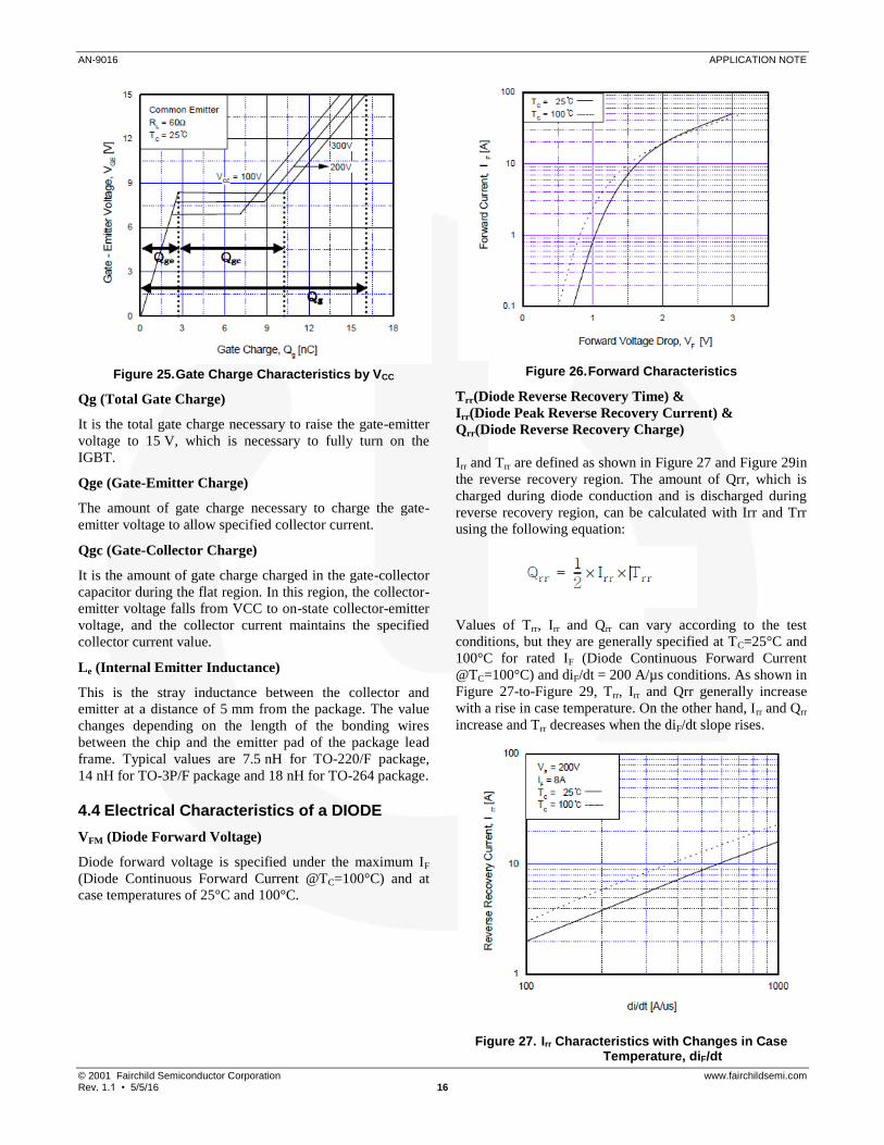
Figure 26. Forward Characteristics
Trr(Diode Reverse Recovery Time) &
Irr(Diode Peak Reverse Recovery Current) &
Qrr(Diode Reverse Recovery Charge)
Irr and Trr are defined as shown in Figure 27 and Figure 29in
the reverse recovery region. The amount of Qrr, which is
charged during diode conduction and is discharged during
reverse recovery region, can be calculated with Irr and Trr
using the following equation:
Values of Trr, Irr and Qrr can vary according to the test
conditions, but they are generally specified at TC=25°C and
100°C for rated IF (Diode Continuous Forward Current
@TC=100°C) and diF/dt = 200 A/µs conditions. As shown in
Figure 27-to-Figure 29, Trr, Irr and Qrr generally increase
with a rise in case temperature. On the other hand, Irr and Qrr
increase and Trr decreases when the diF/dt slope rises.
Figure 27. Irr Characteristics with Changes in Case Temperature, diF/dt

AN-9016 APPLICATION NOTE
© 2001 Fairchild Semiconductor Corporation www.fairchildsemi.com Rev. 1.1 • 5/5/16 17
Figure 28. Qrr Characteristics with Changes in Case
Temperature, diF/dt
Figure 29. Trr Characteristics with Changes in Case Temperature, diF/dt
Figure 27-to-Figure 29 illustrates the test circuit and
waveforms of each part for diode reverse recovery
characteristics.
Figure 30. Diode Reverse Recovery Characteristics Test Circuit & Waveforms

AN-9016 APPLICATION NOTE
© 2001 Fairchild Semiconductor Corporation www.fairchildsemi.com Rev. 1.1 • 5/5/16 18
DISCLAIMER FAIRCHILD SEMICONDUCTOR RESERVES THE RIGHT TO MAKE CHANGES WITHOUT FURTHER NOTICE TO ANY PRODUCTS HEREIN
TO IMPROVE RELIABILITY, FUNCTION, OR DESIGN. FAIRCHILD DOES NOT ASSUME ANY LIABILITY ARISING OUT OF THE APPLICATION OR USE OF ANY PRODUCT OR CIRCUIT DESCRIBED HEREIN; NEITHER DOES IT CONVEY ANY LICENSE UNDER ITS
PATENT RIGHTS, NOR THE RIGHTS OF OTHERS.
LIFE SUPPORT POLICY
FAIRCHILD’S PRODUCTS ARE NOT AUTHORIZED FOR USE AS CRITICAL COMPONENTS IN LIFE SUPPORT DEVICES OR SYSTEMS
WITHOUT THE EXPRESS WRITTEN APPROVAL OF THE PRESIDENT OF FAIRCHILD SEMICONDUCTOR CORPORATION. As used herein:
1. Life support devices or systems are devices or systems which, (a) are intended for surgical implant into the body, or (b) support or
sustain life, or (c) whose failure to perform when properly used in
accordance with instructions for use provided in the labeling, can be reasonably expected to result in significant injury to the user.
2. A critical component is any component of a life support device or system whose failure to perform can be reasonably expected to
cause the failure of the life support device or system, or to affect its
safety or effectiveness.

www.onsemi.com1
ON Semiconductor and are trademarks of Semiconductor Components Industries, LLC dba ON Semiconductor or its subsidiaries in the United States and/or other countries.ON Semiconductor owns the rights to a number of patents, trademarks, copyrights, trade secrets, and other intellectual property. A listing of ON Semiconductor’s product/patentcoverage may be accessed at www.onsemi.com/site/pdf/Patent−Marking.pdf. ON Semiconductor reserves the right to make changes without further notice to any products herein.ON Semiconductor makes no warranty, representation or guarantee regarding the suitability of its products for any particular purpose, nor does ON Semiconductor assume any liabilityarising out of the application or use of any product or circuit, and specifically disclaims any and all liability, including without limitation special, consequential or incidental damages.Buyer is responsible for its products and applications using ON Semiconductor products, including compliance with all laws, regulations and safety requirements or standards,regardless of any support or applications information provided by ON Semiconductor. “Typical” parameters which may be provided in ON Semiconductor data sheets and/orspecifications can and do vary in different applications and actual performance may vary over time. All operating parameters, including “Typicals” must be validated for each customerapplication by customer’s technical experts. ON Semiconductor does not convey any license under its patent rights nor the rights of others. ON Semiconductor products are notdesigned, intended, or authorized for use as a critical component in life support systems or any FDA Class 3 medical devices or medical devices with a same or similar classificationin a foreign jurisdiction or any devices intended for implantation in the human body. Should Buyer purchase or use ON Semiconductor products for any such unintended or unauthorizedapplication, Buyer shall indemnify and hold ON Semiconductor and its officers, employees, subsidiaries, affiliates, and distributors harmless against all claims, costs, damages, andexpenses, and reasonable attorney fees arising out of, directly or indirectly, any claim of personal injury or death associated with such unintended or unauthorized use, even if suchclaim alleges that ON Semiconductor was negligent regarding the design or manufacture of the part. ON Semiconductor is an Equal Opportunity/Affirmative Action Employer. Thisliterature is subject to all applicable copyright laws and is not for resale in any manner.
PUBLICATION ORDERING INFORMATIONN. American Technical Support: 800−282−9855 Toll FreeUSA/Canada
Europe, Middle East and Africa Technical Support:Phone: 421 33 790 2910
Japan Customer Focus CenterPhone: 81−3−5817−1050
www.onsemi.com
LITERATURE FULFILLMENT:Literature Distribution Center for ON Semiconductor19521 E. 32nd Pkwy, Aurora, Colorado 80011 USAPhone: 303−675−2175 or 800−344−3860 Toll Free USA/CanadaFax: 303−675−2176 or 800−344−3867 Toll Free USA/CanadaEmail: [email protected]
ON Semiconductor Website: www.onsemi.com
Order Literature: http://www.onsemi.com/orderlit
For additional information, please contact your localSales Representative
© Semiconductor Components Industries, LLC