Investigation of single crystal germanium pn-junctions for ...
281
Investigation of single crystal germanium pn-junctions for use in tandem CdTe/Ge solar cells by James Ross Sharp B.E. (Hons.), University of Melbourne, 2006 This thesis is submitted to the Faculty of Engineering, Computing and Mathematics of the University of Western Australia in fulfillment of the requirement for the degree of Doctor of Philosophy School of Electrical, Electronic and Computer Engineering 2016
Transcript of Investigation of single crystal germanium pn-junctions for ...

Investigation of single crystal germanium
pn-junctions for use in tandem CdTe/Ge solar cells
by
James Ross Sharp
B.E. (Hons.), University of Melbourne, 2006
This thesis is submitted to the
Faculty of Engineering, Computing and Mathematics
of the University of Western Australia in fulfillment
of the requirement for the degree of
Doctor of Philosophy
School of Electrical, Electronic and Computer Engineering
2016

This thesis entitled:Investigation of single crystal germanium pn-junctions for use in tandem
CdTe/Ge solar cellswritten by James Ross Sharp
has been approved for the School of Electrical, Electronic and ComputerEngineering
Winthrop Professor Lorenzo Faraone
Winthrop Professor and Dean John Dell
Date
The final copy of this thesis has been examined by the signatories, and we findthat both the content and the form meet acceptable presentation standards of
scholarly work in the above mentioned discipline.

3
Sharp, James Ross (B.E. (Hons.))
Investigation of single crystal germanium pn-junctions for use in tandem CdTe/Ge
solar cells
Thesis supervised by Winthrop Professor Lorenzo Faraone
Abstract
Thin film cadmium telluride solar cells are a viable renewable energy tech-
nology, due to low manufacturing cost, fast energy pay-back times, and an energy
gap well matched to the solar spectrum. The technology is already mature and
has commercial application, with more than 10GW of installed thin film CdTe
modules world wide. As with any commercial photovoltaic technology, research
is perpetually focussed on how to boost module efficiency, improve process yield,
and lower production costs. Although startlingly rapid progress has been made
in the field of CdTe photovoltaics in recent years, with commercial CdTe module
manufacturer First Solar reporting record breaking research module efficiencies,
there will inevitably come a point where the performance of CdTe single junction
modules cannot be improved any further, as the conversion efficiency approaches
the Shockley-Queisser limit. At such time, higher efficiencies can only be achieved
by means of adopting multijunction tandem configurations.
This work aims to investigate a possible material combination, namely CdTe
and germanium (Ge), for the advancement of CdTe technology into the realm of
multijunction and concentrated photovoltaics. Germanium is a favourable material
for this purpose due to its narrow energy gap located in a suitable area of the
solar spectrum, availability of large area Ge substrates in epi-ready format, and
idealised electrical and mechanical properties. This thesis investigates germanium

4
processing in a low-cost and manufacturable manner in order to develop a process
for the formation of the lower cell of a multijunction photovoltaic device. Novel
techniques for germanium doping, passivation and contacting are expounded and
a complete methodology for germanium device fabrication is presented. This is of
interest not only to the photovoltaics sector but more generally the techniques are
applicable to a wide range of germanium opto-electronic devices.
In order to predict performance and optimise device structures, simulation
and modelling is undertaken in both a commercial device simulator (Synopsys
Sentaurus Device) as well as in a custom developed analytical/numerical simu-
lation framework. The goal of simulation is to investigate both monolithic and
mechanically stacked configurations and determine which device structure would
be optimal in terms of photocurrent matching and also in terms of optical proper-
ties to minimise optical reflection losses from device active layers. A mechanically
stacked configuration featuring CdTe grown epitaxially on sapphire is considered in
this work and its possible performance compared to a monolithic CdTe/Ge struc-
ture. It is shown that such a structure could contribute an efficiency improvement
of 5.03% absolute over a single junction CdTe solar cell, whereas a monolithic
tandem would boost single junction solar cell efficiency by a mere 3.6% absolute.
Subsequently, doped layers of single crystal germanium were prepared from
bulk germanium wafers utilising spin on dopants, either by directly spinning on a
thin film of dopant, or by vapour transport in the “proximity” doping technique, or
by the novel “sandwich-stacked diffusion” technique developed in this work. These
layers were processed into electronic and photovoltaic devices using standard pro-
cessing techniques, passivated and contacted using the technologies demonstrated
within, and finally characterised. The result is a high quality process for germanium
opto-electronic device fabrication. Optoelectronic devices are shown with surface
recombination velocities as low as 21 cm/s and with specific contact resistivities

5
as low as 1.26 ×10⁻⁷ Ω · cm2 . This highlights the quality of the passivation and
contacting procedures developed in this work.
An investigation of germanium doping for device active region formation
is undertaken. It is concluded that both proximity doping and sandwich-stacked
diffusion yield degenerate p-type doping of germanium and surface concentrations
of up to 1020 atoms cm−3 can be achieved, but degenerate n-type doping can only
be achieved by means of direct spin-on doping. The reason is most likely the high
vapour pressure of phosphorus and its oxides at the processing temperature. Direct
spin on doping gave a maximum donor concentration of 4e19 cm−3, in contrast
with a maximum concentration of 6e18 cm−3 for proximity doping.
Germanium pn-junction devices with ideality factors equal to 1 and showing
breakdown due to Zener effect are presented, as well as a 5.4% efficient solar cell.
The solar cell illustrates the complete germanium diode fabrication process includ-
ing contacting and passivation and the device is shown to be stable in efficiency
when remeasured after eight months. The solar cell was capped with a combined
passivation/anti-reflection solution shown to reduce reflection losses to 6.47%.
Finally, CdTe was grown on both germanium and sapphire substrates and
the results were characterised by a variety of methods including RHEED, XRD,
and optical transmission measurements. CdTe thin films grown on sapphire are
presented with double crystal rocking curve (DCRC) full-width at half maxima
(FWHM) as low as 59 arc seconds as rocked about the 〈111〉 diffraction plane.
CdTe grown on germanium was processed into heterojunction CdTe/Ge P/n junc-
tions and the IV and CV characteristics were measured to elucidate the electronic
properties of the heterojunction. A CdTe/Ge diode with ideality factor n=1.65 is
presented demonstrating reasonable quality material growth and device processing
utilising this novel combination of materials.

Dedication
To my father, Peter, and my mother, Angela and to the love of my life,
Hitomi.

7
Contents
Chapter
1 Introduction 13
1.1 Harnessing the power of the sun . . . . . . . . . . . . . . . . . . 13
1.1.1 Standard solar reference spectrum . . . . . . . . . . . . . 15
1.1.2 A CdTe/germanium solar cell . . . . . . . . . . . . . . . 17
1.1.3 What is cadmium telluride? . . . . . . . . . . . . . . . . 18
1.1.4 What is germanium? . . . . . . . . . . . . . . . . . . . . 19
1.1.5 The Shockley-Queisser limit . . . . . . . . . . . . . . . . 20
1.1.6 Detailed balance limit of efficiency of tandem solar cells . 22
1.1.7 Mechanically stacked vs. monolithic combination . . . . . 24
1.1.8 Development of Cadmium Telluride technology in research
circles . . . . . . . . . . . . . . . . . . . . . . . . . . . 26
1.1.9 Germanium standalone solar cell research . . . . . . . . . 29
1.1.10 Growth of CdTe on germanium . . . . . . . . . . . . . . 31
1.2 Research outcomes and thesis outline . . . . . . . . . . . . . . . 33
2 Analytical and numerical techniques for optoelectronic device modelling 37
2.1 Elementary theory of solar cells . . . . . . . . . . . . . . . . . . 37
2.2 Derivation of an analytical model . . . . . . . . . . . . . . . . . 39
2.2.1 Recombination . . . . . . . . . . . . . . . . . . . . . . . 43

8
2.2.2 Carrier absorption/generation . . . . . . . . . . . . . . . 44
2.2.3 Reflection . . . . . . . . . . . . . . . . . . . . . . . . . 45
2.2.4 Total photocurrent . . . . . . . . . . . . . . . . . . . . . 52
2.2.5 Depletion region width . . . . . . . . . . . . . . . . . . . 52
2.2.6 Dark current . . . . . . . . . . . . . . . . . . . . . . . . 53
2.2.7 Device parasitics . . . . . . . . . . . . . . . . . . . . . . 56
2.2.8 Summary analytical model for solar cells . . . . . . . . . 58
2.2.9 Key device characteristics . . . . . . . . . . . . . . . . . 60
2.2.10 Summary . . . . . . . . . . . . . . . . . . . . . . . . . . 64
2.3 Numerical simulation . . . . . . . . . . . . . . . . . . . . . . . . 65
2.3.1 Introduction . . . . . . . . . . . . . . . . . . . . . . . . 65
2.3.2 Equation set in continuous form . . . . . . . . . . . . . . 65
2.3.3 Dependent variables . . . . . . . . . . . . . . . . . . . . 66
2.3.4 Discretisation of Poisson equation in 1D . . . . . . . . . 67
2.3.5 Discretisation of electron and hole drift-diffusion and con-
tinuity equations in 1D . . . . . . . . . . . . . . . . . . 67
2.3.6 Variable scaling . . . . . . . . . . . . . . . . . . . . . . 69
2.3.7 Solution of discretised equation set over a finite mesh . . 70
2.3.8 Physical models . . . . . . . . . . . . . . . . . . . . . . 88
2.3.9 Test case - Germanium Solar Cell . . . . . . . . . . . . . 98
2.4 Summary and Conclusions . . . . . . . . . . . . . . . . . . . . . 100
3 Device modelling, design and optimisation of tandem II-VI and germanium
solar cells 102
3.1 Introduction . . . . . . . . . . . . . . . . . . . . . . . . . . . . 102
3.1.1 CdTe homojunction on crystalline germanium substrate . 106
3.1.2 Conventional CdTe heterojunction . . . . . . . . . . . . 113

9
3.2 Mechanically stacked tandem solar cell . . . . . . . . . . . . . . 116
3.3 Conclusion . . . . . . . . . . . . . . . . . . . . . . . . . . . . . 119
4 Low-cost techniques for germanium device active region formation 121
4.1 Introduction . . . . . . . . . . . . . . . . . . . . . . . . . . . . 121
4.2 Spin-on dopants . . . . . . . . . . . . . . . . . . . . . . . . . . 121
4.3 Degenerate p-type doping and sandwich stacked diffusion . . . . 122
4.4 Experimental . . . . . . . . . . . . . . . . . . . . . . . . . . . . 123
4.4.1 Sample preparation . . . . . . . . . . . . . . . . . . . . 123
4.4.2 Sandwich-stacked diffusion . . . . . . . . . . . . . . . . 124
4.5 Characterisation . . . . . . . . . . . . . . . . . . . . . . . . . . 128
4.5.1 Sheet resistance measurements . . . . . . . . . . . . . . 128
4.5.2 SIMS profiling . . . . . . . . . . . . . . . . . . . . . . . 130
4.6 Analysis . . . . . . . . . . . . . . . . . . . . . . . . . . . . . . 131
4.6.1 Fitting procedure to extract diffusivities . . . . . . . . . . 131
4.6.2 Thermal activation energy and pre-exponential factor ex-
traction . . . . . . . . . . . . . . . . . . . . . . . . . . . 134
4.7 Proximity doping . . . . . . . . . . . . . . . . . . . . . . . . . . 138
4.7.1 Introduction . . . . . . . . . . . . . . . . . . . . . . . . 138
4.7.2 Experimental - Proximity doping investigation using SIMS 139
4.7.3 Proximity doping with Sb3m Antimony spin-on film . . . 140
4.7.4 Proximity doping with GaB260 spin-on film: Gallium diffusion144
4.7.5 Proximity doping with phosphorus . . . . . . . . . . . . . 147
4.7.6 Direct spin-on doping with phosphorus . . . . . . . . . . 148
4.7.7 Fit to phosphorus depth profiles using non-linear model . 150
4.8 Conclusions . . . . . . . . . . . . . . . . . . . . . . . . . . . . . 153

10
5 Passivation, antireflection, and contacting technologies for germanium opt-
electronic devices 155
5.1 Introduction . . . . . . . . . . . . . . . . . . . . . . . . . . . . 155
5.2 Passivation of germanium . . . . . . . . . . . . . . . . . . . . . 156
5.2.1 Experimental . . . . . . . . . . . . . . . . . . . . . . . . 158
5.2.2 Characterisation . . . . . . . . . . . . . . . . . . . . . . 161
5.2.3 Anti-reflection coatings . . . . . . . . . . . . . . . . . . 165
5.3 Contacts to Germanium . . . . . . . . . . . . . . . . . . . . . . 173
5.3.1 Derivation of specific contact resistivity for some contact
metals . . . . . . . . . . . . . . . . . . . . . . . . . . . 174
5.4 Conclusions . . . . . . . . . . . . . . . . . . . . . . . . . . . . . 183
6 Germanium pn-junction devices 185
6.1 Introduction . . . . . . . . . . . . . . . . . . . . . . . . . . . . 185
6.2 Germanium wafer selection . . . . . . . . . . . . . . . . . . . . 186
6.3 Diode fabrication . . . . . . . . . . . . . . . . . . . . . . . . . . 187
6.3.1 Fabrication process . . . . . . . . . . . . . . . . . . . . . 187
6.3.2 Ge n+/p diodes . . . . . . . . . . . . . . . . . . . . . . 192
6.3.3 Ge n+/p+ “tunnel” diode . . . . . . . . . . . . . . . . . 195
6.4 Investigation of a defective sample using scanning electron microscopy198
6.5 Germanium solar cells . . . . . . . . . . . . . . . . . . . . . . . 199
6.6 Conclusions . . . . . . . . . . . . . . . . . . . . . . . . . . . . . 204
7 II-VI/Germanium Materials Growth and Heterojunction Optoelectronic De-
vices 208
7.1 Introduction . . . . . . . . . . . . . . . . . . . . . . . . . . . . 208
7.2 Choice of materials and crystallography . . . . . . . . . . . . . . 209
7.2.1 Introduction . . . . . . . . . . . . . . . . . . . . . . . . 209

11
7.2.2 Materials science of CdTe/ZnTe/Ge/sapphire . . . . . . . 211
7.3 Material growth techniques . . . . . . . . . . . . . . . . . . . . 219
7.3.1 Introduction . . . . . . . . . . . . . . . . . . . . . . . . 219
7.3.2 Thermal Evaporation . . . . . . . . . . . . . . . . . . . 220
7.3.3 Molecular Beam Epitaxy . . . . . . . . . . . . . . . . . . 222
7.4 Characterisation of thin films . . . . . . . . . . . . . . . . . . . 225
7.4.1 X-ray diffraction . . . . . . . . . . . . . . . . . . . . . . 225
7.4.2 Reflection high-energy electron diffraction (RHEED) . . . 230
7.4.3 Nomarski contrast microscopy . . . . . . . . . . . . . . . 232
7.4.4 Optical constants from transmission measurements . . . . 233
7.5 Electronic properties of the CdTe/Ge interface . . . . . . . . . . 236
7.5.1 Overview . . . . . . . . . . . . . . . . . . . . . . . . . . 236
7.5.2 Fabrication Process . . . . . . . . . . . . . . . . . . . . 236
7.5.3 CdTe Epilayer sheet resistance . . . . . . . . . . . . . . . 239
7.5.4 CdTe / Ge heterojunction current-voltage characteristics . 240
7.5.5 CdTe/Ge heterojunction capacitance-voltage profiling . . 241
7.6 Summary and conclusions . . . . . . . . . . . . . . . . . . . . . 243
8 Conclusions 247
8.1 Summary . . . . . . . . . . . . . . . . . . . . . . . . . . . . . . 247
8.2 Research outcomes . . . . . . . . . . . . . . . . . . . . . . . . . 250
8.3 Future work . . . . . . . . . . . . . . . . . . . . . . . . . . . . 251
8.4 Final Conclusions . . . . . . . . . . . . . . . . . . . . . . . . . . 254

12
Bibliography 256
Appendix
A Decoupled solution - Gummel’s method 267
B Fully coupled solution 270
C List of original contributions in this work 279
D List of publications arising from this work 280
D.1 Conference presentations . . . . . . . . . . . . . . . . . . . . . . 280

Chapter 1
Introduction
1.1 Harnessing the power of the sun
Australia’s potential for photovoltaic power generation ranks high among
that of the world’s nations. With 1.5 million square kilometers of desertified land,
and insolation equivalent to some of the sunniest African nations, there lies in
wait a vast untapped resource. The question then becomes how to harness this
energy and in what form. Solar thermal concentrators seem perfectly suited to the
harsh environment of the Australian desert. These devices concentrate sunlight to
heat up water and create steam. On the other hand, highly efficient, concentrated
photovoltaics (CPV) and solar tracking systems could be the answer. These sys-
tems concentrate sunlight by manipulating a lens to follow the sun throughout the
day and focus it onto small photovoltaic (PV) receivers. These installations can
be highly efficient - over 40 %. With so much land area available, on the other
hand, efficiency may not be so critical so perhaps thin film photovoltaic cells - with
their lower production costs due to reduced material usage - could be a winner to
deliver Australia’s growing energy needs. With much talk at time of writing in the
political sphere about increasing renewable energy targets, perhaps it is a matter
of time before Australia’s uninhabitable areas become centers for national power
generation.
Fig. 1.1 shows the insolation across Australia for a day in summer. With

14
most of the uninhabited areas of Australia receiving 36 MJ/m2, the total amount
of received energy from the sun is unimaginable. For example, If only 0.03% of
Australia’s uninhabited land were utilised for PV power generation, at an efficiency
of just 10%, a peak power of almost 50 GW could be realised, enough to meet all
of Australia’s energy needs for some time to come. In one day in summer around
16 petajoules - that is, 16× 1015 J - would be harvested.
Figure 1.1: Typical Insolation on an Australian summer’s day.Source: Bureau of Meteorology
According to the office of the chief economist, Australia’s current energy
consumption is almost 6,000 petajoules (PJ) per year, of which renewables only
make up 345.7 PJ. Of the renewables, solar PV accounts for a mere 17.5 PJ.
What stimulus is required to tip the balance in favour of renewables? Once again,
motivation in the political sphere may be the answer.

15
In this thesis, we do not attempt to solve Australia’s energy supply problems
once and for all. Instead, we focus on a technology that could one day help bridge
the gap between fossil fuels and renewable energy sources, working in harmony with
other renewable energy technologies for a greener, cleaner future. The technology
we attempt to develop sits somewhere between the concentrated photovoltaics and
the thin film solutions mentioned in the opening paragraph. To set the scene for
our technology, we must first understand the nature of solar energy as it reaches
the Earth’s surface.
1.1.1 Standard solar reference spectrum
0 500 1000 1500 2000 2500 3000 3500 4000
Wavelength, nm
0.0
0.2
0.4
0.6
0.8
1.0
1.2
1.4
1.6
1.8
Sp
ectr
al
Irra
dia
nce
, W
m−
2n
m−
1
AM1.5G spect rum according to ASTM G173-03
Ge
Si
CdTe
ZnTe
Figure 1.2: AM-1.5G Spectrum

16
The radiation from the sun approximates a 5800K blackbody. The radiation
incident on Earth as measured outside the Earth’s atmosphere is termed the air
mass 0, or AM0, spectrum. This radiation strongly resembles standard blackbody
radiation. As the radiation passes through the atmosphere it becomes absorbed
by the molecules that make up the air, particularly water vapour, O2 and CO2.
The radiation spectrum that is incident on the equator is known as AM1, whereas
radiation which passes through the atmosphere at a solar zenith angle of 48.19 is
known as AM1.5. A standardised reference spectrum produced by the American
Society for Testing and Materials (ASTM) is the AM1.5G standard. The “G”
stands for “global tilt” as both direct illumination and diffuse atmospheric reflec-
tions are taken into account by assuming the receiving plane is at a 37 tilt toward
the equator.
The total power density as integrated from the reference spectrum for AM1.5G
is roughly 1000 Wm−2. The spectrum is depicted in Fig. 1.2 and shows the po-
sition in the solar spectrum of the energy gaps of materials under consideration
in this work. Most of the energy is concentrated in the UV-visible portion of the
spectrum, from 400 to 800 nm. A material like Si is capable of absorbing the
bulk of that energy, out to 1100 nm. Germanium however has extended infra-red
absorption and can absorb the radiation out to roughly 1800nm. CdTe on the
other hand only absorbs the red, green and blue / UV portions of the spectrum,
omitting the infrared region entirely. Hence, from the point of view of efficiently
harvesting the solar spectrum with readily available solar materials, a combination
of the two materials could be posited. This would have the advantage of absorb-
ing the solar spectrum efficiently deep into the infrared, with minimal unabsorbed
(hence wasted) energy.

17
1.1.2 A CdTe/germanium solar cell
In this work we propose combining the materials cadmium telluride and
germanium to form a hybrid photovoltaic device known as a tandem solar cell.
CdTe and Ge are both semiconducting materials which have been studied and
used extensively since the advent of the modern era. There are many reasons why
it is desirable to combine materials to form a tandem solar cell. A tandem solar
cell may be more efficient as a whole than any one of its components. This means
that more useful energy is generated from the incident radiation. Although we
have seen that sunlight is abundant in Australia and that a comparatively small
area of land is required to fulfill all of Australia’s energy needs, the cost of raw
materials and production costs to process them need to be brought down to a level
whereby renewable energy technologies can compete with existing fossil fuel based
energy generation technologies. By increasing efficiency more energy is created
per individual photovoltaic module and the production and raw material costs are
thereby offset.
In addition to offsetting the costs, there is potential for raw material reduc-
tion. Reduced usage of scarce raw material and processing is required for energy
generation if module efficiency can be improved. This means, in effect, that less
energy needs to be expended to produce the same power output, effectively short-
ening energy payback times.
By combining materials in a stacked structure (tandem), more of the incident
light can be harnessed and there is less energy that cannot be converted. Since
a solar cell can only convert energy above the energy gap of the materials it
is made from, any sub-band gap radiation is lost; a tandem structure however
features lower-energy gap subcells which absorb this energy. The result is that the
incident spectrum can be more efficiently converted by dividing the spectrum into

18
absorption windows amongst the cells making up the structure.
1.1.3 What is cadmium telluride?
Cadmium is bluish-white metal and element 48 of the periodic table. Cad-
mium is usually produced as a by-product of zinc refining since cadmium is found in
zinc ores. Principal uses for cadmium include cadmium based pigments, favoured
historically due to their lasting characteristics (cadmium red and yellow pigments
do not fade over time in comparison to other pigments), nickel-cadmium (NiCad)
batteries, corrosion resistant plating for steel components, and CdTe solar cells.
Due to the toxicity of Cd, NiCad batteries and cadmium based pigments have
fallen out of favour and non-toxic replacements are usually preferred.
Tellurium is a rare, brittle metalloid with atomic number 52. Tellurium was
first discovered in 1782 by Franz Joseph Muller von Reichenstein. Tellurium is
scarce and has an abundance in the earth’s crust similar to platinum, around 1
ppb, with world reserves of tellurium limited to 24,000 metric tonnes. Tellurium
is mostly obtained from anode sludges produced during copper refinement, but
is also present in some naturally occurring gold ores. Uses for tellurium include
addition to copper to improve machineability without impairing conductivity, to
steel also to improve machineability, to cast iron to help improve the depth of chill,
and to malleable iron as a carbide stabiliser [1]. It has many other industrial uses
including as a vulcanising agent for rubber production and as an additive to glass
(pigment).
CdTe is a compound semiconductor created from the stoichiometric com-
bination of cadmium and tellurium. It has an energy gap of around 1.45 eV [2],
making it a highly suitable solar material. It has the added benefit of being a
potential use for cadmium, which as noted is a by-product of refinement of more
useful zinc. When combined with zinc, the resultant alloy Cd1−xZnxTe is useful

19
for X and gamma ray detection, and when combined with mercury, HgxCd1−xTe
is a strategic material for use in high performance infrared detectors. The primary
industrial use of cadmium telluride is in CdTe solar cells.
1.1.4 What is germanium?
Germanium is a lustrous metalloid with atomic number 32. Germanium was
first predicted by chemist Dmitri Mendeleyev 17 years before its initial discovery.
Mendeleyev was able to predict in advance its mass number, density, oxide and
chloride density and other properties. Mendeleev had named the element ekasil-
icon. Germanium was first discovered in 1885 by the chemist Clemens Winkler
who isolated it from samples of a mineral named argyrodite.
Zinc ores containing germanium are the principal source of germanium pro-
duction worldwide. Germanium is also found in silver, lead and copper ores and
can also be present in some coal deposits. Refinement is usually by roasting the ore
to create germanium oxides followed by conversion to germanium chloride using
hydrochloric acid and finally distillation of the resultant chlorides.
Germanium finds use in modern day electronic applications as part of SiGe
RF-CMOS processes for cutting edge RF technology in laptops, mobile phones,
PDAs and other mobile devices. SiGe is rapidly replacing GaAs based micro-
electronics technology due to lower production costs for comparable devices and
integrability with traditional silicon CMOS processing.
Germanium is a key component in contact formation for GaAs devices for
use in optoelectronics and high frequency applications. Germanium is also used as
a substrate for growth of GaAs-based multijunction solar cells. These are used for
space applications due to their high efficiency (>40%) and for terrestrial concen-
trated photovoltaic (CPV) installations.

20
1.0 2.0 3.0
10
20
30
Ge
SiCdTe
ZnTe
Energy Gap
Effi
cie
ncy
Figure 1.3: Detailed balance limit of efficiency annotated withsome common photovoltaic materials for 1 sun illumination [3]
1.1.5 The Shockley-Queisser limit
Thermodynamic considerations place an upper bound on the efficiency of a
single junction solar cell. By appealing to the principle of detailed balance, i.e.
that each process (in this case absorption of energy) should be equilibrated by its
reverse process, William Shockley and Hans Quisser [3] set out the theoretical limit
for solar cells of a single junction. Fig. 1.3 depicts the detailed balance efficiency
limit for one sun illumination as a function of energy gap and is annotated with

21
some common materials under consideration in this work.
Fig. 1.3 shows that the ultimate efficiency of a CdTe or silicon single
junction solar cell is roughly 30% whereas for a germanium or ZnTe solar cell the
ultimate efficiency is roughly 19%. Obviously from this chart we can gauge the
how far away from the peak efficiency point (roughly 1.3-1.4 eV) we can stray
before suffering a performance degradation. ZnTe and Ge are therefore simply too
distant in energy from the maximum efficiency point to be considered for single
junction operation, but are suitable for use as a component of a multijunction
tandem arrangement.
A multijunction solar cell is a n-junction structure whereby sunlight is har-
vested by two or more solar cells of different energy gaps. Fig. 1.5 gives some
examples of possible tandem solar cell configurations. By way of example, simply
by inspection of Fig. 1.3, the combination of silicon or CdTe in tandem with ger-
manium should allow the germanium solar cell, with its lower ultimate efficiency,
to harvest any photons not collected by the upper cell. The total efficiency of
the device should be roughly equal to the combined individual efficiencies, once
shading of the bottom cell is taken into account. Hence even a naive analysis
shows that the Shockley-Queisser limit for single junction cells can be overcome
by adding more cells to the stack. It must be stressed that thermodynamic laws
have not been violated; but rather the incoming energy is now being converted
more efficiently through spectral splitting between multiple absorbing cells. Solar
cells of 3 or more junctions have been fabricated and are used in space applica-
tions, where the insolation outside earths atmosphere (AM0) is more intense, and
in terrestrial concentrator arrangements, where light is concentrated by a lens to
focus the incoming radiation onto a small photovoltaic device.
Increasing the concentration ratio (the number of “suns”) is another way
to overcome the Shockley-Queisser limit for 1 sun illumination. Again, this does

22
not imply that we have violated thermodynamic laws, but rather that the ultimate
efficiency of a photovoltaic device is actually a function of the power density of
incoming radiation. By increasing the concentration ratio we increase the power
density and shift the detailed balance limit. This is known as concentrated photo-
voltaics. There are some obvious drawbacks to concentrated photovoltaics. Firstly,
the photovoltaic device must be robust enough to handle high solar concentration
ratios without degrading or failing. Secondly, a large lens assembly is required to
focus light onto the concentrated PV device, and this usually requires a tracking
system to follow the sun throughout the day. This adds cost and complexity to
the system as a whole.
1.1.6 Detailed balance limit of efficiency of tandem solar cells
Detailed balance limit of efficiency computations can be performed for tan-
dem solar cells. This yields the efficiency limit as a function of energy gaps for a
particular concentration ratio. For a two junction tandem, a simple contour plot
can be devised which allows the data to be visualised. An excellent reference for
this is De Vos [4]. Such a contour plot is presented in Fig. 1.4.
Fig. 1.4 places the CdTe and Germanium tandem combination on the 40%
isoefficiency curve. While not optimal, the difference between the optimal tandem
combination in terms of ultimate efficiency is not particularly high (2%). Hence
despite being a suboptimal set of energy gaps, purely out of thermodynamic con-
siderations, CdTe and Ge are still well situated in energy space. In this way the
thermodynamic limit of a single junction CdTe solar cell may be circumvented by
the addition of germanium as a lower cell. Hence at a time when CdTe technology
approaches thermodynamic limits, with commercial modules performing close to

23
3
2
1
0 1 2 3
20
30
35
40
4235
30
20
20
CdTe/Ge
tandem
Figure 1.4: Detailed balance limit of efficiency for a two junctiontandem solar cell under 1 sun illumination [4]
theoretical upper bounds, research into tandem cells will become a viable option
to overcome this boundary.
A tandem combination with germanium may also be beneficial from a raw
materials point of view. As mentioned, Te is a rare material and its reserves are
limited. By raising the efficiency of a CdTe module by tandem cell technology, less
scarce tellurium is required to effect the same photovoltaic energy conversion. For
example, since the maximum efficiency of the tandem combination is, in relative

24
terms, greater by more than 25%, less than 3/4 the amount of tellurium is required
for the same power output, lowering the amount of raw material required to achieve
the same end result.
n+ p+p-Ge
Sapphire
Passivation /Anti-reflectionlayer
Grid bars
bottom cell
top cell
Illumination
Buffer layer
p-CdTe absorber
ITO
In grid barAu grid bar
Mechanically stacked tandem
p+ p+p-Ge
Rear contacts
Illumination
Monolithic tandem
p-CdTe
Front contacts Front passivation /
AR coating
CdTe n+ emitter
Tunnel junction +
Ge n+ emitter
Rear passivation
Rear metallisation
Figure 1.5: Mechanically stacked vs. monolithic solar moduleconfigurations
1.1.7 Mechanically stacked vs. monolithic combination
In this work we consider two possible configurations for a tandem CdTe/Ge
photovoltaic device. These are the mechanically stacked and monolithic tandem
configurations, and are depicted in Fig. 1.5. In the mechanically stacked con-
figuration, the two photovoltaic cells forming the tandem device are physically
created separately and then mechanically stacked and interconnected to form a

25
complete electronic device. This has the advantage that device processing is sepa-
rated for both cells which can be of advantage for materials which cannot be easily
combined. Issues which preclude monolithic combination could be low tempera-
ture alloying preventing high temperature processing, lattice mismatch, and other
physical properties that may render the combination awkward from a materials
science perspective.
In the monolithic structure, however, we treat Ge as a substrate for thin
film deposition and grow active device layers on the substrate using a thin film
growth technology like molecular beam epitaxy (MBE) or metal-organic chemical
vapour deposition (MOCVD). This necessitates a certain amount of compatibility
between substrate and epi-layers. For example, heteroepitaxy is difficult if the
lattice constants are not well matched. It is also possible for the substrate to react
with the epilayer material during growth or subsequent processing. Care must
therefore be taken when choosing materials.
Another key difference between monolithic and mechanically stacked tandem
structures is the interconnect between the cells of the tandem. In a mechanically
stacked tandem, the two cells may simply be connected in series provided the
photocurrents are well matched, or the device may not be interconnected at all,
yielding a four terminal device. In a monolithic structure, the interconnect between
the two cells could also be by two or four wire external connection, or by internal
connection consisting of a tunneling/recombination junction (TRJ).
A TRJ is a region of the device where a heavily doped p+/n+ junction
is formed where majority carriers recombine either by band-to-band tunneling
(BTBT) or trap-assisted tunneling (TAT). In BTBT, carriers from the conduc-
tion band on the n+-doped side of the junction tunnel to the valence band of the
p+-doped side and vice versa. In TAT, carriers recombine through traps and defect
states at the interface of the two materials. The key motivation for this type of

26
interconnect is to allow majority carriers of the two series connected sub-cells to
recombine but prevent minority carriers from recombining, allowing a current to
flow through the tandem device. If minority carriers recombine at this interface,
efficiency will be impaired.
1.1.8 Development of Cadmium Telluride technology in research
circles
Cadmium telluride was identified in the 1970’s as a possible solar cell material
due to the existence of low cost fabrication techniques and its high absorption
coefficient [5]. In practical terms this means that thin films of only a micron or
so are sufficiently absorbent of solar radiation for useful photovoltaic conversion.
It was shown that the conversion efficiency of CdTe/CdS solar cells could reach
17% [6], which has been reached and even exceeded in recent years. More modern
estimates show the maximum efficiency to be in excess of 29% [7]. Early research
focused on growing CdS layers on single crystal CdTe substrates using chemical
vapour deposition (CVD) and vacuum evaporation, for which efficiencies peaked
at 10% and 8%, respectively [8].
Chu et al. [9] demonstrated CdTe pn-junctions formed by ion implantation in
1978. The cells demonstrated 3% solar efficiency. It must be noted that the cells
involved were a homojunction type cell, which may explain the poor efficiencies
due to excessive surface recombination loss [7]. Werthen et al. [10] demon-
strated 10.5% efficient CdTe buried homojunctions formed from crystalline CdTe
substrates coated with ITO deposited using electron beam (e-beam) evaporation.
CdS/CdTe heterojunctions formed in an analogous manner were also realized with
efficiencies approaching 7.5%. Matsumoto et al. [11] fabricated 12.8% efficient
CdS/CdTe solar cells using screen printing in 1984. Front contacts were fashioned
from Ag/In and rear contacts from carbon and silver. A small amount of copper

27
(50 ppm) was added to the carbon electrode followed by annealing in nitrogen
atmosphere for 30 minutes at 400C. This was seen to improve efficiency, which
was attributed to p+ doping of the CdTe layer by the copper.
In 1991 Woodcock et al. [12] reported a 10.1% efficient n-CdS/p-CdTe
heterojunction solar cell deposited on tin oxide coated glass. CdS was deposited
from an aqueous solution of cadmium ions with thiourea acting as sulphiding agent
[12]. The CdTe layer was electrodeposited from a cadmium rich electrolyte solution
and was 1.7µm thick. Interestingly, it was found that heat treatment in air in the
range 400-500C converts the CdTe layer to p-type. This is interesting since from
other reports we note that a slight non-stoichiometry alone is enough to cause type
conversion [13]. Large-area cells were fabricated using conventional interconnects
based on laser scribing [12]. The back contact was formed on a CdTe surface
which was modified to be tellurium rich, thus lowering contact resistance.
In 1993 Britt and Ferekides [14] reported highly efficient CdTe solar cells
manufactured using chemical bath deposition (CBD) of the cadmium sulphide
(CdS) window layer and close spaced sublimation (CSS) of the p-type cadmium
telluride layer. The efficiency was reported to be 15.8% under AM1.5 illumination.
In the first step of manufacture, fluorine doped SnO2 films were deposited on glass
using MOCVD to provide a low resistance contact to the CdS layer. Next the CdS
window layer was formed using CBD. The thickness of the films was typically 0.07
- 0.1 µm. Prior to CdTe deposition, the structures were annealed for 5-20 minutes
in a hydrogen atmosphere. This was found to improve fill factor in the final device
structure. Next, CdTe was deposited using CSS from a 99.999% purity cadmium
telluride source. Typically, 5 µm thick CdTe was deposited.
In 2001, Wu et al [15] presented high efficiency polycrystalline thin film so-
lar cells with efficiencies of 16.5% and fill factors higher than 77% percent. The
structures used departed significantly from the more conventional SnO2/CdS/CdTe

28
makeup and instead created window/top contact layers from CTO (cadmium stan-
nate) to improve fill factor and ZTO (zinc stannate) to improve reproducibility of
the cells. The CTO and ZTO films were first deposited using RF magnetron sput-
tering and varied from 100-300 nm in thickness. The cadmium sulphide layer was
deposited using chemical bath deposition (CBD) and the cadmium telluride layer
was deposited using CSS, as in conventional methods for CdTe solar cell fabrica-
tion. The CdTe was deposited at 570-625C for 3-5 minutes in O2/He atmosphere
[15], and after CdTe deposition the cells were subjected to CdCl2 treatment for
15 minutes at 400-430C to promote re-crystallisation of the CdTe. This is a typ-
ical step in CdTe solar cell processing, often referred to as activation. The back
contact was formed by a layer of CuTe:HgTe-doped graphite paste, followed by a
layer of silver paste [15].
In 1996, Shao et al [16] demonstrated an 11.6% efficient RF magnetron-
sputtered thin-film CdTe solar cell. The same group [17] demonstrated improved
formation of CdTe solar cells using RF-magnetron sputtering in 2004. In this
case, the transparent conducting oxide (TCO) was aluminium doped zinc oxide
(ZnO:Al), since it shows excellent transparency over the entire visible spectrum
[17]. This TCO is not normally used since it reacts with CdS under the high
temperatures required for close spaced sublimation or due to environmental inter-
actions during electroplating. RF sputtering, being a low temperature deposition
technique does not require such extreme temperatures and hence allows ZnO:Al
to be explored as a possible TCO. Hall measurements showed ZnO:Al to have
higher mobility than the more usual fluorine-doped tin oxide (SnO2:F). To further
compare the two TCOs, cells were created on ZnO:Al/aluminosilicate glass (ASG)
and SnO2:F soda lime glass (SLG) by depositing 0.13 µm CdS and 2.3 µm CdTe
by RF magnetron sputtering at 250C. Cells were activated using CdCl2 treatment
at 387C. Efficiency was 14% for the ZnO:Al cell and 12.6% for the SnO2:F cell.
29
ZnO:Al cells however showed higher performance degradation (42.7% as opposed
to 27.1%) under stressing/light soak conditions, which was attributed to lower
thermal stability or interdiffusion across the ZnO/CdS interface.
The most spectacular advancement in CdTe solar cell technology came as
CdTe solar panel manufacturer First Solar demonstrated a string of record module
efficiencies over the past five years culminating in a 21.5% efficient cell first shown
in early 2015 [18]. Unfortunately, the manufacturer is very secretive about techni-
cal details and the precise mechanism by which the efficiency of their modules was
improved. For example, did they alter deposition processes to improve lifetimes,
or did they focus instead on doping the CdTe with a suitable acceptor to gain on
open circuit voltage, or perhaps they invented a novel technology for back con-
tact formation to reduce contact resistance and improve fill factor, or finally did
they concentrate on window and buffer layer optimisation to allow for better light
penetration to the absorber layer, or perhaps even some combination of these? In
any case, the result demonstrates how far CdTe technology has come in over 35
years of continuous development as illustrated in Fig. 1.6 in terms of efficiencies
achieved.
1.1.9 Germanium standalone solar cell research
Stand-alone germanium solar cells have received considerable research inter-
est for their use in tandem/concentrator cells, usually in combination with GaAs
top absorbers for space applications. They have also received attention for use in
thermophotovoltaic (TPV) systems.
Venkatasubramanian et al. [19] presented a 9% efficient (AM0) germanium
solar cell as a part of an investigation of Ge and Si0.07Ge0.93 solar cells for bottom

30
3
5
7
9
11
13
15
17
19
21
Effi
cie
ncy
1980
1983
1986
1989
1992
1995
1998
2001
2004
2007
2010
2013
2016
Chu et al.
Wethen et a
l.Matsu
moto
et al.
Woodcock et al.
Britt &
Fere
kides
Shao et al.
Wu et al.
Shao et al.
First
Solar inc.
Year
Figure 1.6: CdTe solar cell research milestones
cells in tandem structures for space applications in 1991. The junctions were
grown by chemical vapour deposition (CVD) at reduced pressures. The germanium
devices were grown at temperatures ranging from 600 to 800C. The junctions were
mostly p-on-n structures. The base regions were 6 µm and the emitters ranged
from 0.2 - 1µm in thickness. An AlGaAs passivation layer was used, which led to
an almost 20% improvement in external quantum efficiency.
Khvostikov et al. [20] demonstrated 5% efficient (AM1.5D, 100 suns) ger-
manium solar cells realised with ZnS/MgF2 antireflection coatings for thermopho-
tovoltaic applications. Junctions were formed by diffusion of zinc into n-type
germanium substrates. A layer of LPE grown p-type GaAs was used for surface
passivation which improved output voltage and efficiency.
Posthuma et al. [21] demonstrated a 6.7% efficient (AM1.5) stand-alone
germanium solar cell in 2003. The shallow emitter was realised using a phosphorus-
containing spin-on dopant source. Diffusion time was kept short to reduce surface
roughening and realise a shallow emitter, and in a similar fashion the diffusion
31
temperature was optimised. For passivation, a thin layer of amorphous silicon was
deposited using plasma-enhanced chemical vapour deposition (PECVD). A silver
finger pattern served as front contact and was diffused through the passivation
layer. This innovation was necessary to circumvent the lack of a uniform wet etch
with high selectivity between the amorphous silicon and germanium. Finally an
anti reflective-coating of ZnS and MgF2 was applied.
The same authors [22] reported an improved efficiency of 7.8% (AM1.5G)
in 2007. The fabrication process was essentially identical, however it featured
contacts formed from a thin layer of palladium and a thick layer of silver (as
opposed to the aluminium used in earlier studies) which helped to improve cell fill
factor reproducibility.
These results are summarised in Fig. 1.7.
1.1.10 Growth of CdTe on germanium
Cadmium telluride has previously been grown on germanium substrates using
molecular beam epitaxy (MBE). Matsumura et al. [23] prepared CdTe 〈111〉 and
CdTe 〈100〉 on 〈111〉 and 〈100〉 Ge substrates. The growth temperature ranged
between 150 C and 400 C .
It was noted that as crystallinity improved with growth temperature, the
films became milky in appearance. Two effusion cells were used during growth,
Cd at 290 C and Te at 405 C . From these nominal temperatures, flux ratio was
varied between 1/5 to 5/1. It was found that at ratios 1/2 - 1/5 (Cd:Te) the film
was polycrystalline. Twinning was observed on 〈111〉 substrates but not on 〈100〉
substrates. X-ray diffraction showed decrease of the rocking curve full-width at
half maximum (FWHM) for increasing substrate temperature, up to 350 C .
Zanatta et al. [24] presented 〈211〉B CdTe films grown on 〈211〉 Ge sub-
strates at a growth temperature of 250 C . During growth the temperature was

32
ramped to 320 C to optimize the crystal quality. The growth rate was 45 nm
per minute. Double crystal rocking curves (DCRC) for x-ray diffraction gave the
average FWHM of 89 arc seconds with a std. deviation of 6 arc seconds.
5
6
7
8
9
Effi
cie
ncy
1990
1993
1996
1999
2002
2005
2008
Venkatasu
bram
anian
(AM0)
Year
Khvostiko
v
Posthum
aPosth
uma
Figure 1.7: Ge solar cell research milestones
The efforts of Zanatta et al. came about in the context of HgCdTe growth on
CdTe buffer layers. HgCdTe is a high performance infrared detector material that,
despite its excellent characteristics for IR detector applications, has the unfortunate
disadvantage that it lacks a high quality large area lattice matched substrate.
HgCdTe is lattice matched to Cd0.95Zn0.05Te but substrates are difficult to fabricate
in large area format due to brittle mechanical characteristics [24, 25]. Hence
alternative substrates such as Si, GaAs and Ge have been considered for HgCdTe
growth. Ge has a better coefficient of thermal expansion and lattice constant
match with HgCdTe in comparison to silicon, hence the choice as a potential
substrate candidate.

33
In this work we consider the use of Ge not only as a potential substrate but
also as an active device layer with photovoltaic devices formed prior to CdTe epitax-
ial growth. This would necessitate altered growth conditions to prevent damage to
the underlying germanium device during epitaxial growth. As a substrate, Ge still
has the unfortunate disadvantage of lattice mismatch (14%) with CdTe, however
this is more favourable than silicon (19%). Germanium is chosen predominantly for
more efficient spectral splitting as opposed to lattice matching. Since Ge has the
narrower energy gap, it can absorb the longer wavelength photons out to roughly
1800 nm, whereas silicon can only absorb out to roughly 1100nm. This extra ab-
sorption region should allow for better matching of photocurrents between the two
cells of the tandem stack. The ability to absorb longer wavelength photons as well
as match the photocurrents between the two cells should allow for the creation of
an efficient two junction solar cell, with potentially higher efficiency than its single
junction CdTe counterpart.
1.2 Research outcomes and thesis outline
From the discussion in Section 1.1.8 it is evident that good progress has been
made over the past 35 years in CdTe processing technology. With the efficiency
of single junction CdTe solar cells now having been demonstrated at 21.5%, the
pathway towards the ultimate efficiency (≃30%) of single junction CdTe seems
comparatively free of encumbrance. However when that ultimate efficiency is to
all intents and purposes reached, progress can only be made by expanding into the
realm of multi junction solar cells. The aim of this work is not to advance single
junction CdTe processing any further, since this sphere of research is being under-
taken at commercial scale by manufacturers with significant research expertise and,
due to their vested interest in the development of CdTe technology, commensurate
research budgets. We assume in this work that CdTe single junction technology

34
has already developed to the point where a tandem configuration is justified, and
we will concentrate on development of the Ge bottom cell and interconnect.
In Section 1.1.9 the progress of standalone germanium solar cells was out-
lined. The conversion efficiencies at one-sun are quite low in the results hitherto
published for germanium solar cells; it begs the question how much of an efficiency
improvement can be expected from the addition of a germanium bottom cell to
form a multijunction solar cell. Device processing techniques would need to be
advanced further until single junction germanium solar cells yielded efficiencies of
10% or more to add substantial improvement to CdTe solar cell efficiency in a tan-
dem configuration. For example, while theoretically any efficiency improvement
is significant, the extra expense may not be justifiable. The research challenges
are therefore how to reduce surface recombination in Ge standalone solar cells
with adequate surface passivation, how to make low resistivity contacts to germa-
nium, and how to form device regions in a low cost manner without any unwanted
contamination which may impair device efficiency.
This investigation therefore expands upon the work of Posthuma et al. [21,
26, 22, 27, 28] to improve upon device active region formation, passivation and
contacting technologies developed by this group in order to further germanium
standalone solar cell research, as well as investigating properties of the CdTe/Ge
heterojunction. Materials growth draws on research by Zanatta et al. [24, 29] to
develop a process for growing CdTe epitaxially on Ge.
We now turn our attention to investigating these research challenges in the
following chapters. In Chapter 2, we explore analytical and numerical simulation of
photovoltaic devices and create a simple simulation framework for the evaluation
of single junction solar cells. This framework consists of both well-known closed
form solutions of the drift-diffusion equations as well as a compact numerical drift-
diffusion solver that discretises and solves these equations over a small mesh. The

35
purpose of developing this framework is to add insight into numerical simulation
and complement more complicated commercial device simulators.
In chapter 3 we consider, simulate and optimise the device structures. We
do so by employing a commercial simulator application and our self-developed
simulation framework to simulate devices by solving the drift-diffusion equations for
solar cells illuminated by the solar spectrum. Of particular importance is matching
the photocurrent between the two cells, particularly in a monolithic configuration.
A comparison is made between monolithic and mechanically stacked tandem solar
cells. For the case of a mechanically stacked tandem, photocurrents are matched
so that the individual sub-cells can be series connected to form a two terminal
device.
Chapter 4 considers low cost techniques for junction formation for germa-
nium optoelectronic devices. Doping of bulk germanium is considered using spin-on
dopants, silica or polymer films which are spun onto a target wafer to deliberately
introduce impurity atoms into device regions. Three techniques are presented for
device active region formation, these being “sandwich-stacked” diffusion, proximity
doping, and direct spin-on doping. The three methods give the three possible con-
figurations for doping germanium in a low cost manner by either direct contact or
vapour transport. Hence a proof-of-concept of all three techniques demonstrates
possible avenues for low cost manufacture of germanium sub-cells for multijunction
tandem application.
Chapter 5 examines passivation, antireflection and contacting techniques for
germanium optoelectronic devices. We consider a range of chemical pre-treatments
and passivation layers and compare their efficacy by measuring the lifetime using
a simple photoconductive decay apparatus. Wet and dry chemical pre-treatments
are necessary to prepare the sensitive germanium surface prior to passivation layer
deposition. This is done so by terminating dangling bonds at the highly chemi-

36
cally reactive germanium surface so that when the passivation layer is deposited
the complete structure is comparatively free of recombination centers and defects.
This is critical to high performance photovoltaic devices. Investigated passiva-
tion layers are inductively coupled plasma enhanced chemical vapour deposition
(ICPECVD) grown thin films. The advantage of using an ICPECVD reactor to
deposit the passivation layer is the potential for in-situ dry pre-treatments with re-
active gases, and it is found that in-situ ammonia pretreatment increases minority
carrier lifetime.
In Chapter 6, we investigate materials growth of CdTe and ZnTe on sapphire
and germanium, and investigate the properties of a CdTe/Ge heterojunction. CdTe
and ZnTe thin films on germanium and sapphire are prepared using molecular
beam epitaxy (MBE) and thermal evaporation, respectively, and are characterised
by a variety of methods including RHEED, optical transmission methods, and
X-ray diffraction (XRD). A sample of CdTe grown on a germanium substrate is
processed into a heterojunction device and the electronic properties are investigated
by measuring the IV and CV characteristics.
Chapter 7 summarizes and makes conclusions about the work as a whole.

Chapter 2
Analytical and numerical techniques for optoelectronic device modelling
2.1 Elementary theory of solar cells
2.1.0.1 Theory of pn junctions
A pn junction is a semiconducting device that consists of two doped regions,
one doped p-type, that is to say, doped with acceptors, and the other doped n-
type, that is, with donors. By bringing these two semiconducting regions together,
a potential barrier known as the built-in potential is formed at the metallurgical
junction, which can be used to separate charge carriers, and hence produce a
photocurrent when illuminated.
Fig. 2.1 shows the pn junction at equilibrium. The symbols used are ex-
plained in Tab. 2.1. Diagram a) shows the space-charge distribution, b) the
electric field distribution, c) the potential and d) the energy band diagram. At
equilibrium, the differing signs of the charge on either side of the junction brings
about the space-charge region. Here, local electric fields cause carriers to cross
the metallurgical junction at x = 0 to cancel out the imbalance of carriers. The
space-charge or depletion region then becomes depleted of carriers, and an electric
field develops across the junction, with a built-in potential ψbi . This forces the
Fermi-level to sit level within the device.
It is this built-in potential that sweeps carriers out of the junction if they
enter it, and in particular separates electron-hole pairs into their constituent parts,

38
i.e. electron and hole. In this way, minority carriers can be swept across the
junction to become majority carriers and be collected at the contact. This is the
basic principle by which pn-junction solar cells operate.
d)
c)
b)Area = built in potential,
a)
+
-
0
0
depletion region
Depletion charge
p-region n-region
Donor density
Acceptor density
Figure 2.1: pn junction at equilibrium, after [30]

39
ND the donor doping density
NA the acceptor doping density
WDp the width of the depletion region in the p-type material
WDn the width of the depletion region in the n-type region
E the electric field
Em the maximum electric field
ψbi the built-in potential
ψp the potential in the p-type region
ψn the potential in the n-type region
ψBp
the energy difference between the
intrinsic level and the Fermi level
in the p type region
ψBn
the energy difference between the
intrinsic level and the Fermi level in
the n type region
φp
the energy difference between the
valence band and the Fermi level in
the p-type region
φn
the energy difference between the
conduction band and the Fermi level
in the n-type region
Table 2.1: Symbols for Fig. 2.1
2.2 Derivation of an analytical model
Whilst solar cells are becoming increasingly complicated in terms of device
structure, necessitating complex numerical simulation techniques for their analysis,
simplified analytical models can be derived subject to certain assumptions. An

40
analytical model can be used as an adjunct to a more thorough numerical model,
and has the following advantages:
• An analytical model will yield results much faster than a numerical simu-
lation (which may take hours to converge), facilitating experimentation.
• An analytical model may help to verify results from numerical simulation.
• Analytical models give rise to closed form expressions for determining the
effect of parameter variation on key device metrics.
Analytical solutions can be obtained for the light and dark currents in the
three regions of a p-n junction solar cell, subject to certain simplifying assumptions.
These are well known and can be found in many references, such as [31]. These
solutions are derived in the following section to lay the foundation for the analytical
model. The pn-junction structure under consideration is depicted in Fig 2.2. Here,
x is defined to be the position within the cell, with x = 0 set to be at the
metallurgical junction. H is the total width of the cell, and Hp and Hn are the
widths of the p and n type regions respectively. Wn and Wp are the widths of
the depletion region in the n and p-type regions respectively and W is the total
depletion region width.
Figure 2.2: Cell considered for derivation of an analytical model[31]

41
In deriving an analytical model, we begin with the following assumptions
[31]:-
• The analysis is restricted to one dimension.
• Light is incident normal to the surface, and we neglect scattering and
internal reflection.
• Both regions of the pn junction are non-degenerate and donors/acceptors
are fully ionized.
• There are no hot carrier effects and a photon excites a single electron-hole
pair.
• Minority carrier recombination is pseudo-first order in the bulk and at the
surfaces.
• Low level minority carrier injection/diffusion is the operative transport
mechanism.
• Device parasitics are ignored (we will consider them later using a circuit
analysis approach).
By assuming that minority carrier injection and diffusion are the only opera-
tive modes of transport, that we can ignore device parasitics, and further that the
cell remains in low injection throughout the bias/optical excitement range [31],
we can appeal to the principle of superposition and essentially decouple the light
and dark current densities, so that they can be modelled separately and the results
superposed, greatly simplifying the results.
When modelling the electrical properties of semiconductors, we solve the
following set of equations:-

42
∇2φ(x) = −∇E(x) = − 1
ǫǫ0ρ(x) (2.1)
Je(x) = q · (n(x) · µe · E(x) + Dn · ∇n(x)) (2.2)
Jh(x) = q · (p(x) · µh · E(x)− Dp · ∇p(x)) (2.3)
1
q∇ · Je(x)− re(x) + ge(x) = 0 (2.4)
−1
q∇ · Jh(x)− rh(x) + gh(x) = 0 (2.5)
Where φ(x) is the potential at x, E(x) is the electric field at x, ρ is the
space charge, ǫ is the relative permittivity of the material, ǫ0 is the vacuum per-
mittivity, Je and Jh are the electron and hole current densities, respectively, q is
the elementary charge, n(x) and p(x) are the electron and hole concentrations
respectively, re and rh are the electron and hole recombination rates respectively,
and ge and gh are the electron and hole generation rates, respectively. Equation
2.1 is the Poisson equation, Eqns. 2.2, 2.3 are the electron and hole drift-diffusion
equations, and Eqns. 2.4/2.5 are the electron and hole continuity equations.
By restricting ourselves to one dimension, we can differentiate Eqn. 2.2 and
substitute it into Eqn. 2.4. The procedure is then repeated for holes, yielding the
following set of equations which can be solved to yield the carrier concentrations
in the device [31]:-
Dn
d2n
dx+ µeE
dn
dx+ nµe
dE
dx− re(x) + ge(x) = 0 (2.6)
Dp
d2p
dx− µhE
dp
dx− pµh
dE
dx− rh(x) + gh(x) = 0 (2.7)

43
2.2.1 Recombination
For the recombination terms in Eqns. 2.6 and 2.7, we assume low injection
conditions and hence that recombination in the semiconductor is pseudo-first order
[31]. Hence the recombination rates may be written as [31]:-
re(x) =np − n0p
τe=
De(np − n0p)
L2e0 ≤ x ≤ Hp (2.8)
rh(x) =pn − p0
n
τh=
Dh(pn − p0n)
L2h−Hn ≤ x ≤ 0 (2.9)
Where np is the electron concentration in the p region, pn is the electron
concentration in the n region, De and Dh are the electron and hole diffusivities
respectively, Le , Lh are the electron and hole diffusion lengths respectively, and n0p
and p0n are the dark minority carrier densities.
The diffusion length for electrons and holes is given by [32]:-
Le =√
Deτ (2.10)
Lh =√
Dhτ (2.11)
where τ is the bulk lifetime for electrons and holes.
2.2.1.1 Surface recombination velocity
Surface recombination velocity is the rate at which carriers recombine at sur-
faces. These surfaces include the front and back surfaces of a solar cell as well as
any grain boundaries within the cell if it consists of polycrystalline material. Grain
boundaries act as recombination centers because the lattice is unterminated and
there are a great many defects and dangling bonds at such sites. The interfaces
between layers within the solar cell also act as surfaces, with a certain surface re-
combination velocity used to express the recombination rate due to surface effects.

44
Passivation is necessary to adequately terminate the crystal lattice at such
sites to reduce recombination rates and hence lower surface recombination velocity.
By passivating defects such as dangling bonds at surfaces and grain boundaries,
that is, rendering them inert, recombination can be prevented in such areas. This
will serve to increase charge collection probability, since carriers now have a lower
probability of recombining at interfaces and grain boundaries and hence more
chance of being collected at contacts.
In the context of analytical models, surface recombination velocity is usually
a boundary condition imposed on surfaces, i.e.
Dh
dp
dx
∣
∣
∣
∣
x=surface
= Sp · p|x=surface (2.12)
In analytical simulations of a single dimension, this parameter is used to
model the effectiveness of contacts to allow majority carriers to recombine in
preference to minority carriers, which determines the charge collection probability.
Hence in a single dimension, where the surface beyond the contact region cannot
be accounted for, surface recombination velocity at the contact itself is used to
encompass surface effects at cell front and back surfaces. Although Ohmic con-
tacts are usually considered to be sites of infinite recombination, the use of this
parameter in a one-dimensional simulation serves to factor in surface effects and
model the quality of device passivation for a particular cell.
2.2.2 Carrier absorption/generation
We now consider the generation of carriers in the semiconductor. These are
given by the so called Beer-Lambert expression, as follows [31]:

45
g ne (x) =g n
h (x) = αnλφ
emitterλ exp[−αn
λ(Hn + x)] − Hn ≤ x ≤ 0 (2.13)
g pe (x) =g
ph (x) = αp
λφbaseλ exp[−αp
λ(x −Wp)] 0 ≤ x ≤ Hp (2.14)
where αnλ and αp
λ are the absorption coefficients in the n and p regions,
respectively, and φemitterλ and φbase
λ are the photon fluxes into the emitter and base
region, respectively, as given by [31]:
φemitterλ = φ0
λ(1− rλ) photons ·m−2s−1 (2.15)
φbaseλ = φemitter
λ exp(−αnλHn)exp(−αp
λWp) photons ·m−2s−1 (2.16)
where φ0λ is the illumination, and rλ is the reflectivity for the wavelength
under consideration.
The absorption coefficients ανλ where ν ∈ (n, p) can be taken from tables
of the complex refractive index of the material, since the absorption coefficient is
related to the imaginary part (or k-value) of the complex refractive index [30]:
α =4πkrλ
(2.17)
2.2.3 Reflection
When two media of differing refractive index meet, light incident on the
interface will be partially reflected, partially absorbed, and partially transmitted.
This leads to a decrease in efficiency in solar cell devices, since any light reflected
from the air-semiconductor interface cannot contribute to the photocurrent.
To this end, solar cells front surfaces are usually capped with an antireflection
coating, which may consist of multiple layers of different materials. Antireflection

46
coatings are designed to give the lowest possible reflectance for the widest possible
region of the solar spectrum, in order to maximize cell efficiency.
The propagation of light in the system can be modelled using the direct
matrix method [33], [34]:-
Meq =
n∏
j=1
cos(φj)iηjsin(φj)
iηj sin(φj) cos(φj)
(2.18)
where Meq is the characterisation matrix of the thin film stack, nj is the
refractive index of the j th layer, φj =2πλneffj dj ,ηj = Y0njcos(θ) for parallel polari-
sation, ηj = Y0nj
cos(θ)for perpendicular polarisation, θj is the angle of incidence in
layer j , Y0 is the admittance of free space, and dj is the thickness of the j th layer.
From this, the characteristic matrix of the assembly can be written down:
B
C
= Meq
1
ηs
(2.19)
where ηs is the effective complex refractive index of the substrate similarly
defined as above.
The reflectance, R , transmittance, T , and absorption, A of the assembly of
j thin film layers can be obtained as follows [34]:
R =
(
η0B − C
η0B + C
)(
η0B − C
η0B + C
)∗(2.20)
T =4η0Re(ηs)
(η0B + C )(η0B + C )∗(2.21)
A = 1− R − T =4η0Re(BC
∗ − ηs)
(η0B + C )(η0B + C )∗(2.22)
To compute the reflectance at the top active layer (usually emitter) of a
solar cell, a matrix stack of all thin films from the illumination source to the
active layer is assembled for all wavelengths of the spectrum. The transmission

47
and reflectance can then be computed using the above relations. This yields the
incident light for all wavelengths of the spectrum for the topmost active region of
the solar cell. From there, the solar cell’s efficiency can be calculated. Note: this
does not incorporate reflection from the cell’s bottom contact and hence multiple
passes through the device. This is because the analytical models presented in this
work only compute photocurrents for a single pass of illumination.
2.2.3.1 Emitter (n-type) quasi-neutral region
In the emitter region we consider the current from minority carrier holes.
To obtain the hole concentration throughout the emitter (−Hn ≤ x ≤ −Wn), we
first substitute Eqn. 2.9 into Eqn. 2.7, then based on our assumption that the
carrier concentrations obey the principle of superposition, we subtract the terms
involving the dark hole concentration [31], yielding a differential equation solely
for the photo-generated holes in the n region (=pphn ) [31]:
Dh
d2pphn
dx2− Dhp
phn
L2h+ g n
λ (x) = 0 (2.23)
Note that the terms involving E are set to zero since there is no electric field
in the quasi-neutral region. Solutions to this equation will yield the carrier gener-
ation profile as a function of x for a particular wavelength of light, λ. Solutions
can be obtained subject to the following boundary conditions [31]:
pphn (−Wn) = 0 (2.24)
Dh
dpphn
dx
∣
∣
∣
∣
x=−Hn
= Sppphn (−Hp) (2.25)
These boundary conditions state that the hole concentration is zero at the
edge of the space charge region, and that the rate at which holes leave through

48
the front contact is equal to the front hole surface recombination velocity Sp times
the hole concentration at that point.
Equation 2.23 is an inhomogeneous second order differential equation, hence
its solution is of the form [31]:-
pphn (x ,λ) = CF + PI (2.26)
CF, the complementary function, is the solution of 2.23 with g nλ(x) set to
zero, and is of the form [31]:-
CF = Aphin cosh
(
x
Le
)
+ Bphin sinh
(
x
Le
)
(2.27)
The particular integral PI is some constant C times Eqn. 2.14. To find the
constant C, we simple set the CF to zero and substitute Eqn. 2.26 into Eqn. 2.23
[31]:-
PI =Cφemitterλ exp[−αn
λ(Hn + x)] = C · y (x)
⇒Dh
d2C · y (x)dx2
− DhC · y (x)L2h
+ y (x) = 0
⇒C
(
Dh(αnλ)
2 − Dh
L2h
)
+ 1 = 0
∴ C =− L2hDh[(αn
λ)2L2h − 1]
With some algebra, the solution for the hole density can be obtained [31]:-
49
pphn (x ,λ) =
φemitterλ αn
λL2h
Dh[(αnλ)
2L2h − 1]exp(−αn
λQn)
×
cosh[(Hn + x)/Lh] + (ShLh/Dh) sinh[(Hn + x)/Lh]
+(αnλLh + ShLh/Dh) sinh[−(Wn + x)/Lh]exp(α
nλQn)
cosh(Qn/Lh) + ShLh/Dh sinh (Qh/Lh)− exp[−αn
λ(Wn + x)]
(2.28)
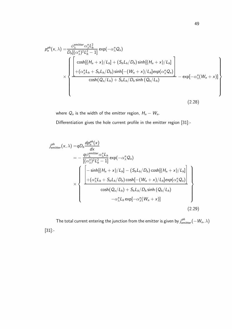
where Qn is the width of the emitter region, Hn −Wn.
Differentiation gives the hole current profile in the emitter region [31]:-
jphemitter (x ,λ) =qDh
dpphn (x)
dx
=− qφemitterλ αn
λLh
[(αnλ)
2L2h − 1]exp(−αn
λQn)
×
− sinh[(Hn + x)/Lh]− (ShLh/Dh) cosh[(Hn + x)/Lh]
+(αnλLh + ShLh/Dh) cosh[−(Wn + x)/Lh]exp(α
nλQn)
cosh(Qn/Lh) + ShLh/Dh sinh (Qh/Lh)
−αnλLh exp[−αn
λ(Wn + x)]
(2.29)
The total current entering the junction from the emitter is given by jphemitter (−Wn,λ)
[31]:-

50
jphemitter (−Wn,λ) =− qφemitter
λ αnλLh
[(αnλ)
2L2h − 1]exp(−αn
λQn)
×
− sinh[Qn/Lh]− (ShLh/Dh) cosh[Qn/Lh]
+(αnλLh + ShLh/Dh) exp(α
nλQn)
cosh(Qn/Lh) + ShLh/Dh sinh (Qh/Lh)
−αnλLh
(2.30)
2.2.3.2 Base (p-type) quasi-neutral region
The solution for the photocurrent in the base quasi-neutral region is found
in a similar way, by solving electron continuity equation for the minority carrier
electron concentration in the region Wp ≤ x ≤ Hp [31]:-
De
d2nphp
dx2−
Denphp
L2p+ g
pλ (x) = 0 (2.31)
The solution takes the following form [31]:-
jphbase(x ,λ) =− qφbase
λ αpλLe
(αpλ)
2L2e − 1
×
− sinh[(Hp − x)/Le]− (SeLe/De) cosh[(Hp − x)/Le]
−(αnλLe − SeLe/De) cosh[(x −Wp)/Le ]exp(−αp
λQp)
cosh(Qp/Le) + SeLe/De sinh (Qp/Le)
+αpλLe exp[−α
pλ(x −Wp)]
(2.32)
where Qp is the width of the base region, Hp−Wp. The photocurrent density
flowing into the junction is given by jphbase(Wp,λ) [31]:-

51
jphbase(Wp,λ) =− qφbase
λ αpλLe
(αpλ)
2L2e − 1
×
− sinh[Qp/Le ]− (SeLe/De) cosh[Qp/Le]
−(αnλLe − SeLe/De) exp(−αp
λQp)
cosh(Qp/Le) + SeLe/De sinh (Qp/Le)
+αpλLe
(2.33)
2.2.3.3 Space-charge region
In deriving the current in the space charge region, we may consider either
electrons or holes; here a choice is made in favour of electrons. The assumption in
the space-charge region is that carriers are swept out by the built-in electric field
sufficiently quickly that no recombination occurs [31]. Hence, Eqn. 2.4 reduces
to:-
1
q
dJe
dx+ ge(x) = 0 (2.34)
This can be solved using simple integration to yield jphscr . To simplify the
integration, the problem can be made symmetric about the origin, x = 0. Defining
the illumination at this point as:-
φjnλ = φemitter
λ exp(−αnλHn) (2.35)
and defining the generation of carriers in the SCR:-
gλ(x) =
αnλφ
jnλ exp(−αn
λx) −Wn ≤ x ≤ 0
αpλφ
jnλ exp(−α
pλx) 0 ≤ x ≤ Wp
(2.36)
We can now integrate the carrier generation in the SCR to find the photocurrent:-

52
jphscr =− q
∫ Wp
−Wn
gλ(x)dx
=− q
(∫ 0
−Wn
αnλφ
jnλ exp(−αn
λx)dx +
∫ Wp
0
αpλφ
jnλ exp(−α
pλx)dx
)
=− qφjn [exp(αnλWn)− exp(−αn
λWp)] (2.37)
2.2.4 Total photocurrent
The total photocurrent for a single wavelength λ is simply the sum of the
previously derived photocurrents for the emitter, base, and space-charge regions
[31]:-
jph(λ) = jphemitter (−Wn,λ) + jphscr (λ) + j
phbase(Wp,λ) (2.38)
The total photocurrent is then the integral over all wavelengths of the illu-
mination spectrum [31]:
jph =
∫
AM1.5G
jph(λ) dλ (2.39)
2.2.5 Depletion region width
The depletion region width for a homojunction can be found by adopting the
exhaustion layer (Schottky) approximation. This allows the following expressions
to be derived [31]:-
Wn =NA
NA + ND
W (2.40)
Wp =ND
NA + ND
W (2.41)
W =
[
2ǫ0ǫps ǫ
nsψbi(NA + ND)
2
qNAND(ǫpsNA + ǫnsND)
]1/2
(2.42)

53
The built-in potential ψbi is given by [30]:-
ψbi = kT lnNDNA
n2i(2.43)
For a heterojunction, the depletion region width is given by [30]:-
WD1 =
[
2NA2ǫs1ǫs2(ψbi − V )
qND1(ǫs1ND1 + ǫs2NA2)
]1/2
(2.44)
WD2 =
[
2ND1ǫs1ǫs2(ψbi − V )
qNA2(ǫs1ND1 + ǫs2NA2)
]1/2
(2.45)
where WDn is the width of depletion region n, ǫsn is the dielectric constant
of region n, NDn is the donor concentration in region n, NAn is the acceptor
concentration in region n, ψbi is the built-in potential, and V the applied potential.
The built-in potential of the heterojunction is given by [35]:-
qψbi =∆EC −∆EV
2+ kTln
NdNa
ni ,n + ni ,p(2.46)
where ∆EC and ∆EV are the conduction and valence band discontinuities
respectively, Nd and Na are the doping densities either side of the heterojunction,
and ni ,p and ni ,n are the intrinsic carrier concentrations in the p and n regions,
respectively.
2.2.6 Dark current
2.2.6.1 Emitter dark current
Minority carrier holes are considered when computing the emitter dark cur-
rent in the n-type emitter region, in an analogous manner to that of section
2.2.3.1. Substituting Eqn. 2.9 into Eqn. 2.7 and dropping the electric field and
carrier generation terms, yields [31]:-

54
Dp
d2pDKn
dx− Dh(p
DKn − p0
n)
L2h= 0 (2.47)
which can be solved subject to the following boundary conditions [31]:-
De
dpDKn
dx
∣
∣
∣
∣
∣
x=−Hn
= Sh[pDKn (−Hn)− p0
n] (2.48)
pn(−Wn) = p0n exp(qVj/kT) (2.49)
where Eqn. 2.48 states that the flux of minority carriers at the emitter surface
(i.e. the front contact) is equal to the surface recombination velocity times the
number of carriers present at the surface. Equation 2.49 arises from the so-called
low-level injection conditions [31] and gives the minority carrier concentration at
the edge of the junction for some junction bias Vj .
The solution can be shown to take the following form [31]:-
pDKn (x) =p0
n + p0n[exp(qVj/kT)− 1]
×
cosh[(Hn + x)/Lh] + (ShLh/Dh) sinh[(Hn + x)/Lh]
cosh(Qn/Lh) + (ShLh/Dh) sinh(Qn/Lh)
−Hn ≤ x ≤ −Wn
(2.50)
Substituting into Eqn. 2.3 gives the hole current density profile in the emitter
[31]:-
jDKemitter (x) =
qDhp0n
Lh[exp(qVj/kT)− 1]
×
sinh[(Hn + x)/Lh] + (ShLh/Dh) cosh[(Hn + x)/Lh]
cosh(Qn/Lh) + (ShLh/Dh) sinh(Qn/Lh)
(2.51)
At the edge of the junction, i.e. at x = −Wn, the current flowing into the
emitter can be expressed as [31]:-

55
jDKemitter (−Wn) =
qDhp0n
Lh[exp(qVj/kT)− 1]Ξn (2.52)
where Ξn is the emitter width factor, given by [31]
Ξn =sinh[Qn/Lh] + (ShLh/Dh) cosh[Qn/Lh]
cosh(Qn/Lh) + (ShLh/Dh) sinh(Qn/Lh)(2.53)
2.2.6.2 Base dark current
The expressions for the dark electron density and electron current density
profile are derived in an identical manner to that of section 2.2.6.1. They are as
follows [31]:-
nDKp (x) =n0p + n0p[exp(qVj/kT)− 1]
×
cosh[(Hp − x)/Le ] + (SeLe/De) sinh[(He − x)/Le ]
cosh(Qp/Le) + (SeLe/De) sinh(Qp/Le)
Wp ≤ x ≤ Hp
(2.54)
jDKbase(x) =
qDen0p
Le[exp(qVj/kT)− 1]
×
sinh[(Hp − x)/Le] + (SeLe/De) cosh[(Hp − x)/Le]
cosh(Qp/Le) + (SeLe/De) sinh(Qp/Le)
(2.55)
As in section 2.2.6.1, the current flowing into the base from the junction at
x = Wp can be expressed as [31]:-
jDKbase(Wp) =
qDen0p
Le[exp(qVj/kT)− 1]Ξp (2.56)
where Ξp is the base width factor, given by [31]:-
Ξp =sinh[Qp/Le ] + (SeLe/De) cosh[Qp/Le ]
cosh(Qp/Le) + (SeLe/De) sinh(Qp/Le)(2.57)

56
2.2.6.3 Space-charge region dark current
In the dark space charge region Eqn. 2.6, and Eqn. 2.7 become [31]:-
Dn
d2n
dx+ µeE
dn
dx+ nµe
dE
dx= 0 (2.58)
Dp
d2p
dx− µhE
dp
dx− pµh
dE
dx= 0 (2.59)
Their solution is quite involved and can be found in [31]. However, since in
the dark space charge region there is (effectively) no generation or recombination,
it follows that the dark current density in the space charge region is constant.
On the assumption that all majority carriers injected at one end of the junction
become minority carriers when emerging from the space-charge region, the dark
current in the space-charge region can be expressed as [31]:-
jDKscr = jDK
emitter (−Wn) + jDKbase(Wp)
=
[
qDhp0n
LhΞn +
qDen0p
LeΞp
]
[exp(qVj/kT)− 1] (2.60)
Which reduces to the Shockley equation for Ξn = Ξp = 1 [31].
2.2.7 Device parasitics
Device parasitics can be conveniently modelled as two parasitic resistors, one
in series and one in parallel. The series resistance is the lumped total of contact
resistance, which itself can be resolved into contributions from the semiconduc-
tor/metal interface as well as the metallisation itself, and any bondout resistance.
The shunt resistance encompasses a variety of processes that act like a simple
resistance in parallel with the device. This could be due to pin holes and defects
that shunt out the emitter, or lateral defects causing junction shunting current to
flow at the edges of the mesa.
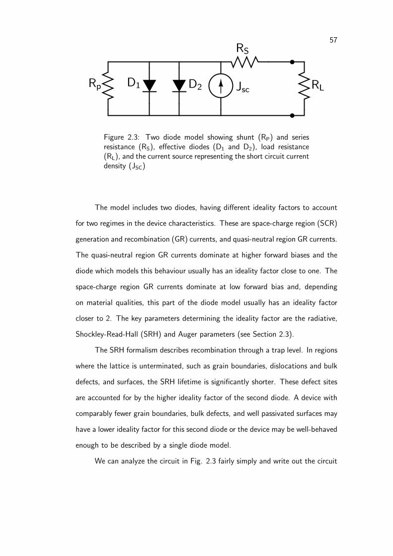
57
Figure 2.3: Two diode model showing shunt (RP) and seriesresistance (RS), effective diodes (D1 and D2), load resistance(RL), and the current source representing the short circuit currentdensity (JSC)
The model includes two diodes, having different ideality factors to account
for two regimes in the device characteristics. These are space-charge region (SCR)
generation and recombination (GR) currents, and quasi-neutral region GR currents.
The quasi-neutral region GR currents dominate at higher forward biases and the
diode which models this behaviour usually has an ideality factor close to one. The
space-charge region GR currents dominate at low forward bias and, depending
on material qualities, this part of the diode model usually has an ideality factor
closer to 2. The key parameters determining the ideality factor are the radiative,
Shockley-Read-Hall (SRH) and Auger parameters (see Section 2.3).
The SRH formalism describes recombination through a trap level. In regions
where the lattice is unterminated, such as grain boundaries, dislocations and bulk
defects, and surfaces, the SRH lifetime is significantly shorter. These defect sites
are accounted for by the higher ideality factor of the second diode. A device with
comparably fewer grain boundaries, bulk defects, and well passivated surfaces may
have a lower ideality factor for this second diode or the device may be well-behaved
enough to be described by a single diode model.
We can analyze the circuit in Fig. 2.3 fairly simply and write out the circuit
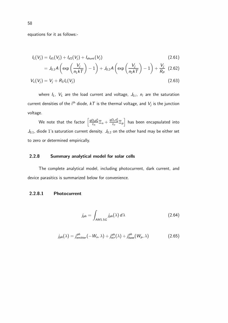
58
equations for it as follows:-
IL(Vj) = Id1(Vj) + Id2(Vj) + Ishunt(Vj) (2.61)
= J0,1A
(
exp
(
Vj
n1kT
)
− 1
)
+ J0,2A
(
exp
(
Vj
n2kT
)
− 1
)
+Vj
RP
(2.62)
VL(Vj) = Vj + RS IL(Vj) (2.63)
where IL, VL are the load current and voltage, J0,i , ni are the saturation
current densities of the ith diode, kT is the thermal voltage, and Vj is the junction
voltage.
We note that the factor[
qDhp0n
LhΞn +
qDen0p
LeΞp
]
has been encapsulated into
J0,1, diode 1’s saturation current density. J0,2 on the other hand may be either set
to zero or determined empirically.
2.2.8 Summary analytical model for solar cells
The complete analytical model, including photocurrent, dark current, and
device parasitics is summarized below for convenience.
2.2.8.1 Photocurrent
jph =
∫
AM1.5G
jph(λ) dλ (2.64)
jph(λ) = jphemitter (−Wn,λ) + jphscr (λ) + j
phbase(Wp,λ) (2.65)

59
jphemitter (−Wn,λ) =− qφemitter
λ αnλLh
[(αnλ)
2L2h − 1]exp(−αn
λQn)
×
− sinh[Qn/Lh]− (ShLh/Dh) cosh[Qn/Lh]
+(αnλLh + ShLh/Dh) exp(α
nλQn)
cosh(Qn/Lh) + ShLh/Dh sinh (Qh/Lh)
−αnλLh
(2.66)
jphscr =− q
∫ Wp
−Wn
gλ(x)dx
=− q
(∫ 0
−Wn
αnλφ
jnλ exp(−αn
λx)dx +
∫ Wp
0
αpλφ
jnλ exp(−α
pλx)dx
)
=− qφjn [exp(αnλWn)− exp(−αn
λWp)] (2.67)
jphbase(Wp,λ) =− qφbase
λ αpλLe
(αpλ)
2L2e − 1
×
− sinh[Qp/Le ]− (SeLe/De) cosh[Qp/Le]
−(αnλLe − SeLe/De) exp(−αp
λQp)
cosh(Qp/Le) + SeLe/De sinh (Qp/Le)
+αpλLe
(2.68)
2.2.8.2 Darkcurrent
jDK (Vj) =
[
qDhp0n
LhΞn +
qDen0p
LeΞp
]
[exp(qVj/kT)− 1] (2.69)
jDK ,parasitics(Vj) = J0,1
(
exp
(
Vj
n1kT
)
− 1
)
+ J0,2
(
exp
(
Vj
n2kT
)
− 1
)
+vj
RP
(2.70)
VL(Vj) = Vj + RS IL(Vj) (2.71)

60
2.2.8.3 Total current
jtotal(Vj) =
∫
AM1.5G
jph(λ) dλ− jDK ,parasitics(Vj) (2.72)
2.2.9 Key device characteristics
There are several key parameters that can be extracted from solar cell device
characteristics that allow the performance of a cell to evaluated and compared with
other devices. These can be summarised as follows:-
• Short Circuit Current
• Open Circuit Voltage
• Fill Factor
• Efficiency
2.2.9.1 Short circuit current
The short circuit current (i.e. when the load is effectively a short circuit) is
roughly equivalent to the photocurrent, since at zero bias the dark current should
be zero. In practice, due to recombination effects which are not included in the
idealised diode model (Auger recombination, GR currents, trap-assisted and band
to band tunneling, shunting effects due to process related defects etc.) this may
not be the case and a very small leakage current may exist, as evidenced in the
dark IV characteristics. In general, however, at zero bias these effects are much
smaller than the photocurrent and can be neglected.
Short circuit current is therefore related to the number of photons absorbed
by the device. This necessitates adequate collection of incoming photons by en-
suring they are absorbed in the device and not lost due to reflection or inefficient

61
absorption. Hence the absorber layer must account for reflections at the front
surface and prevent photons from being lost due to optical mismatch between the
front surface and the atmosphere, as well as ensuring that any unabsorbed photons
do not exit from the rear surface, but are, in fact, reflected at the rear surface and
hence absorbed on a second or further pass through the device. Better yet would
be a light trapping design that traps photons and keeps them confined within the
body of the device due to total internal reflection.
From Eqn. 2.66 and Eqn. 2.68, it is evident that diffusion length, diffusivity,
and surface recombination velocity play a vital role in determining the probability
of photo-generated electron-hole pairs reaching a contact for collection. In order
to maximise photocurrent, surface recombination velocities must be minimised,
and diffusivity (i.e. mobility) must be maximised, in so doing improving diffusion
length. To lower surface recombination velocities, front and rear surfaces must
be adequately passivated. This necessitates combined passivation/antireflection
coatings that terminate the semiconductor surface as well as providing light trap-
ping properties. To improve diffusion lengths, mobilities must be optimised. This
necessitates high quality materials with good electronic properties. Single crystal
semiconducting devices will always outperform polycrystalline and amorphous thin
films in this regard, at the expense of increased material cost. The same can
be said of lifetimes, also a component in determining diffusion lengths. Hence
there is a trade off between material cost and electronic properties when choosing
materials to optimise photocurrents.
2.2.9.2 Open circuit voltage
Open circuit voltage conditions occur when the photocurrent exactly cancels
the dark current, yielding no net current. For this case we can write:-

62
jph =
[
qDhp0n
LhΞn +
qDen0p
LeΞp
]
[exp(qVoc/kT)− 1]
⇒ exp(qVoc/kT) = 1 +jph
qDhp0n
LhΞn +
qDen0pLe
Ξp
⇒ Voc =kT
qln
1 +jph
qDhp0n
LhΞn +
qDen0pLe
Ξp
(2.73)
giving the open circuit voltage of the cell, Voc . Since the open circuit voltage
is essentially determined by the ratio of the light and dark currents, it is necessary to
maximise the photocurrent whilst minimising the dark current to optimise the open
circuit voltage. This means that many of the the material parameters affecting
the photocurrent also determine the open circuit voltage, i.e. diffusion length,
diffusivity, and surface recombination velocity. In addition, open circuit voltage is
determined by the emitter and base doping densities. By increasing the doping
densities, dark current can be reduced, improving open circuit voltage. It can be
seen from equation Eqn. 2.73 that if the photocurrent were directly scaled, for
example by using a lens to concentrate the incident radiation, the open circuit
voltage would increase. In this way, the power increases with concentration of the
incoming solar radiation. This power increase is the principle by which concentrated
photovoltaics (CPV) is feasible.
2.2.9.3 Efficiency
Efficiency is defined as the ratio of the output power to the incident power,
or
η =Pout
Pin
× 100% (2.74)
Pin for AM1.5G illumination is 100 mW/cm2. Efficiency is determined by
the maximum output power of the device, at the device maximum power point,

63
since power output is determined by the load. To optimise efficiency therefore, the
position of the maximum power point must be optimised. This means optimising
not only short circuit current and open circuit voltage, but also fill factor, as
discussed in the next section. This is where device parasitics come into play as the
series and shunt resistance of the device shift the position of the maximum power
point, affecting the efficiency.
2.2.9.4 Fill factor
Voltage, Volts
Cell PV
Curr
ent
Area b
Area a
Pow
er
Cell JV
FF=Area b / Area a x 100%
Figure 2.4: Graphical depiction of maximum power point, opencircuit voltage, short circuit current, and fill factor and theirrelationship.
Fill factor is the geometric ratio of the area bounded by the maximum power
point and the open circuit voltage/short circuit current. This relationship is de-
picted graphically in Fig. 2.4.
FF =Jmpp · Vmpp
Jsc · Voc
× 100% =η × Pin
Jsc × Voc
(2.75)

64
Factors determining the fill factor include recombinative losses, since both
current and voltage are determined by diffusion length and surface recombination
velocity, and series resistance. Series resistance shifts the position of the maximum
power point back toward the current axis. Shunt resistance shifts the position of
the maximum power point down towards the voltage axis. Hence we need low
recombination losses, low series resistance and high shunt resistance to optimise
fill factor and hence efficiency.
2.2.10 Summary
A review of analytical solutions to the drift-diffusion equations has been
presented. From this, an analytical model for solar cells has been built up including
a discussion of device parasitics. The closed form nature of the analytical model
and governing equations means that a device can be modelled quickly. This allows
back-of-the-envelope calculations for novel device structures to be carried out
quickly, as a preparation for more detailed numerical calculations, which solve
the drift-diffusion equations numerically using finite element analysis rather than
rely on closed-form solutions allowing more complicated models to be evaluated.
We turn our attention to such solutions in the next section.

65
2.3 Numerical simulation
2.3.1 Introduction
In this section, numerical solution of the drift-diffusion equations is pre-
sented. This involves discretisation and solution of the drift-diffusion equations,
as well as discussion of various models of interest. The purpose of this section is
to build up a stand-alone unidimensional drift-diffusion solver for numerical simu-
lation of solar cells. This is a useful exercise that allows one to gain insight into
the function of numerical simulators, which are very complex and quite difficult to
understand at first.
2.3.2 Equation set in continuous form
The drift-diffusion set of equations belongs to a class of problems collectively
known as diffusion-advection-reaction problems. Their numerical solution is known
to be problematic, and this is particularly the case when dealing with semiconductor
problems, as the tight coupling between potential and carrier concentrations intro-
duces non-linearities which impair numerical stability. In this section we present the
unidimensional discretisation and possible solution methods for the drift-diffusion
equations.
The drift-diffusion set of equations for the steady state behaviour of an
electronic device were presented in Section 2.2.
The discretisation of the electron and hole drift-diffusion and continuity equa-
tions (equations 2.2 - 2.5) over a mesh is itself problematic since a non-linear in-
terpolation is usually necessary to determine mesh points on the odd grid (for first
differences) as required for solution of the electron and hole continuity equations.

66
2.3.3 Dependent variables
We will mainly consider the set of dependent variables (φ, n, p) for electron
and hole concentration and potential, respectively. However, it is possible to
work with other sets of dependent variables. One particular example is the set of
variables (φ, u, v ) where u and v are given by:-
n = ni · exp(
φ
kT
)
· u (2.76)
p = ni · exp(
− φ
kT
)
· v (2.77)
Although it is fairly obvious that the dynamic range required by this variable
set is very large, to the extent that practical implementation even on modern
computers is very difficult [36].
Another such variable set is (φ, φn, φp), where raw carrier concentrations
are replaced by quasi-Fermi potentials according to the following relation:-
n = ni · exp(
φ− φn
kT
)
(2.78)
p = ni · exp(
φp − φ
kT
)
(2.79)
Finally another set of dependent variables are the Slotboom variables, (φ,
Φn, Φp) where:-
Φn = ni · exp(
− φn
kT
)
(2.80)
Φp = ni · exp(
φp
kT
)
(2.81)
however, it is noted that this formulation is difficult to extend to degenerate
conditions. Although the variables (φ, n, p) seem the most natural choice for

67
solving semiconductor problems, a change of variables is often advantageous to
circumvent the problems associated with the non-linearity and tight coupling of
the drift-diffusion model.
2.3.4 Discretisation of Poisson equation in 1D
The Poisson equation is comparatively easily discretised, since the Laplacian
operator requires only physical mesh points (not odd grid, or interpolated, mesh
points) since it is discretised by a second difference, and so the Poisson equation
(2.1) becomes (see e.g. [36]):-
Fφ(φ, n, p)|i = ǫǫ0
(
φxi−1− φxi
xi − xi−1
+φxi+1
− φxi
xi+1 − xi
)
2
xi+1 − xi−1
−e·(n − p − ND + NA) = 0
(2.82)
where the subscripts i , i − 1 etc. refer to the mesh point.
2.3.5 Discretisation of electron and hole drift-diffusion and continuity
equations in 1D
After combining Eqns. 2.2 and 2.4, the following expression can be discre-
tised to yield a function Fn(φ, n, p).
∇ · (n(x) · µe · E(x) + Dn · ∇n(x))− re(x, n, p,φ) + ge(x) = 0 (2.83)
The difficulty in discretisation lies in the terms in n, the electron concentra-
tion, which require first differences. This requires construction of an ”odd grid”,
with interleaved mesh points, or as more commonly used, a non-linear interpola-
tion. If the first differences are naively computed this will lead to poor convergence
and generation of artifacts. The most common interpolation is the scheme due

68
to Scharfetter and Gummel, and involves solution of the drift-diffusion equations
between physical mesh points under the assumption that the partial derivative in
φ is constant [36], which can be assumed valid for arbitrarily fine meshes. This
gives rise to the following so called growth function for interpolation [36]:-
g(x ,φ) =1− exp
(
φi+1−φi
kT· x−xixi+1−xi
)
1− exp(
φi+1−φi
kT
) (2.84)
The electron concentration at the mesh midpoint is therefore given by the
following relation [36]:-
Jn,i+1/2 =µn(xi) · kT
q·(
ni+1 · B(φi+1−φi
kT)− ni · B(φi−φi+1
kT)
xi+1 − xi
)
(2.85)
The analogous relation for the hole concentration can be similarly derived.
By approximating the divergence operator with a simple first difference, the 1D
discretisation can be completed as follows.
Fn(φ, n, p)|i =2µn(xi) · kT
q · (xi+1 − xi−1)
·(
ni+1 · B(φi+1−φi
kT)− ni · B(φi−φi+1
kT)
xi+1 − xi− ni · B(φi−φi−1
kT)− ni−1 · B(φi−1−φi
kT)
xi − xi−1
)
− R(xi ,φ, n, p) + G (xi) = 0 (2.86)
Here B(y ) is the Bernoulli function defined by [36]
B(y ) =y
ey − 1(2.87)
and G (x) and R(x ,φ, n, p) are the local generation and recombination, re-
spectively.
Similarly, the discretisation of the analagous relations for holes can be derived
[36].

69
Fp(φ, n, p)|i = − 2µp(xi) · kTq · (xi+1 − xi−1)
·(
pi+1 · B(φi−φi+1
kT)− pi · B(φi+1−φi
kT)
xi+1 − xi− pi · B(φi−1−φi
kT)− pi−1 · B(φi−φi−1
kT)
xi − xi−1
)
− R(xi ,φ, n, p) + G (xi) = 0 (2.88)
These discretisations can be readily extended to two and three dimensions,
although for higher dimensionality alternate discretisations are possible using box
integration or the finite volume method.
2.3.6 Variable scaling
Variable scaling is important for solving semiconductor problems since scalars
have very different magnitudes if raw SI (or cgs) units are used. For example,
potential in eV and carrier concentration in cm−3 differ on average by 10-20 orders
of magnitude.
Furthermore, it can be shown from singular perturbation theory that for
small λ (where λ is the characteristic Debye length of the device region of interest)
the coupled system becomes well conditioned in the variable set (φ, u, v ) [37, 36].
Hence scaling is required to reduce the λ as small as possible. This can be achieved
by scaling voltage units by kT , the thermal voltage.
Many sets of scaling units have been proposed. The system adopted in this
work for numerical scaling is based on cgs units and is simple and effective. It has
been shown to bring about rapid convergence for the solvers used herein, and is
presented in Tab. 2.2.
Scaling of lengths (e.g. cm) can be either by a constant or in terms of
maximum doping concentration (Nmax), multiplied by 1e3. The latter has the
advantage that for low doped devices the residual is comparable, since it has

70Parameter Unit Scale ValueLength cm 1e8 or 1e3× 3
√Nmax
Second s 1e8Potential V 1/kTCharge C 1/q
Temperature K 1/300
Table 2.2: Scaling parameters for numerical simulation used inthis work
approximately the same weight irrespective of doping concentration, so that a
constant definition of the maximum residual for convergence (i.e. tolerance) can
be used (e.g. 1e-16) for different types of devices.
2.3.7 Solution of discretised equation set over a finite mesh
2.3.7.1 Iterative methods
The above set of non-linear discretised equations in one dimension can only
be solved by means of an iterative procedure, such as Newton’s method [36].
f(y) = 0 (2.89)
For the system described by Eqn. 2.89, Newton’s method involves iteratively
stepping from an initial guess of the solution toward a local minimum by means
of the following relation [36]:
yk+1 = yk −f(yk)
f ′(yk)(2.90)
where xk is the solution vector at the k th iteration step. Reformulating Eqn.
2.89 to suit solution Eqn. 2.82, Eqn. 2.86 and Eqn. 2.88, we may write:

71
yk+1 =
φk+1
nk+1
pk+1
(2.91)
=
φk
nk
pk
−
∂Fφ
∂φ
∂Fφ
∂n
∂Fφ
∂p
∂Fn
∂φ∂Fn
∂n∂Fn
∂p
∂Fp
∂φ∂Fp
∂n∂Fp
∂p
−1
Fφ(φk , nk , pk)
Fn(φk , nk , pk)
Fp(φk , nk , pk)
(2.92)
= yk − J−1F(yk) (2.93)
Iteration is performed until the residue given by ||F(yk)|| is less than some
predetermined tolerance value.
The difficulty in solution using the fully-coupled Newton’s method lies in
the tight coupling of the equations, specifically since carrier concentrations are a
non-linear function (exponential) of the potential term φ. Furthermore, Newton’s
method for a system of coupled non-linear equations in three variables (which
are themselves row vectors with entries for each mesh point) reduces to a matrix
inversion problem which is computationally expensive since the Jacobian has 3N×
3N entries.
Furthermore, the computation of the Jacobian matrix, let alone its inverse,
is complex and cumbersome. It is possible to compute an exact Jacobian matrix
by manually calculating analytical functions to generate the Jacobian matrix en-
tries as well as estimating the Jacobian using finite differences (inexact Jacobian).
Nevertheless, this approach is computationally expensive in and of itself.
It is possible to employ decoupled solution methods to ease the burden of
these computations. We now introduce Gauss-Seidel iteration, an iterative solu-
tion method for the decoupled solution of coupled non-linear PDEs, and present
Gummel’s method, a simple but effective solution method for semiconductor prob-

72
lems.
2.3.7.2 Gauss-Seidel iteration
Gauss-Seidel iteration can be used to decouple the drift-diffusion model equa-
tions. If the Jacobian matrix can be assumed definite and all blocks on its main
diagonal are non-singular [36] we may decompose the Jacobian into an upper and
lower triangular matrix in order to decouple the system as follows [36]:
∂Fφ
∂φ0 0
∂Fn
∂φ∂Fn
∂n0
∂Fp
∂φ∂Fp
∂n∂Fp
∂p
k
·
δφk
δnk
δpk
m+1
= −
Fφ(φk , nk , pk)
Fn(φk , nk , pk)
Fp(φk , nk , pk)
−
0∂Fφ
∂n
∂Fφ
∂p
0 0 ∂Fn
∂p
0 0 0
k
·
δφk
δnk
δpk
m
(2.94)
where the column vector
([
δφk δnk δpk
]m)T
represents the mth “inner”
iterate for solution for the correction vector,
([
δφk δnk δpk
])T
, from which
the state vector over the mesh can be computed by the relation [36]:
φk+1 = φk + δφk
nk+1 = nk + δnk
pk+1 = pk + δpk
The system Eqn. 2.94 can be decoupled and the partial derivatives resub-
stituted to yield a set of three equations that are solved separately using iterative
techniques [36]:

73
∂F kφ
∂φ· δφk,m+1 = −Fφ(φk , nk + δnk,m, pk + δpk,m) (2.95)
∂F kn
∂n· δnk,m+1 = −Fn(φk + δφk,m+1, nk , p
k + δpk,m) (2.96)
∂F kp
∂p· δpk,m+1 = −Fp(φk + δφk,m+1, nk + δnk,m+1, pk) (2.97)
The problem again reduces to solution of a set of linear equations for the vec-
tor(
[
δφk δnk δpk
]m+1)T
. The process is repeated until ||(Fφ, Fn, Fp)||k,m+1 < ǫ,
i.e. less than some pre-determined tolerance figure.
However, the precise formulation of the functions Fφ, Fn, Fp will doubtless
have a big impact on convergence. Performance is usually quite poor if the variable
set is chosen as the natural variables φ, n, p, however better convergence may be
achieved by reformulating and linearising the variable set φ, u, v introduced in
Section 2.3.3.
In the next section we consider an implementation of Gauss-Seidel iteration
in the form of Gummel’s method.
2.3.7.3 Gummel’s method
Derivation
In order to decouple the system of equations, Gummel’s method relies on
reformulation of the Poisson equation to include non-linear terms in the carrier
concentrations, which helps to bring about better convergence since the carrier
concentrations vary wildly during iterative solution of the Poisson equation. These
non-linear terms arise from the reformulation of the Poisson equation for the de-
pendent variable set (φ, u, v ) [36]:

74
∇2φ− e
ǫǫ0·(
exp
(
φ
kT
)
· u − exp
(−φkT
)
· v − ND + NA
)
= 0 (2.98)
If Eqn. 2.98 is solved using an iterative procedure, i.e. Newton’s method,
then this equation itself can be decoupled to solve for φk+1 (the potential term
for the k + 1th iterate) in terms of uk , vk . Furthermore, resubstituting the natural
variables nk , pk in terms of φk and collecting terms gives the following non-linear
equation:-
∇2φ− e
ǫǫ0· (nk ·
(
exp
(
φk+1 − φk
kT
)
− 1
)
+ nk
− pk ·(
exp
(
−φk+1 − φk
kT
)
− 1
)
− pk − ND + NA) = 0 (2.99)
This equation can be linearized and greatly simplified using a truncated series
expansion of the exponential, i.e.,
exp(x) = 1 + x +x2
2!+
x3
3!... ≃ 1 + x (2.100)
which gives:
∇2φ − e
ǫǫ0·((
nk + pk
kT· (φk+1 − φk)
)
+ nk − pk − ND + NA
)
= 0 (2.101)
Discretisation in one dimension
Following from this we may write out the set of discretised equations to be
solved in turn as part of a decoupled iterative solution algorithm.

75
Fφ(φ, n, p)|i ,k+1 = ǫǫ0
(
φi−1,k+1 − φi ,k+1
xi − xi−1
+φi+1,k+1 − φi ,k+1
xi+1 − xi
)
2
xi+1 − xi−1
− e ·(
n1,k + p1,k
kT· (φi ,k+1 − φi ,k)
)
− e · (ni ,k − pi ,k − ND + NA) = 0 (2.102)
Fn(φ, n, p)|i ,k+1 =2µn(xi) · kTxi+1 − xi−1
· (ni+1,k+1 · B(φi+1,k+1−φi ,k+1
kT)− ni ,k+1 · B(φi ,k+1−φi+1,k+1
kT)
xi+1 − xi−
ni ,k+1 · B(φi ,k+1−φi−1,k+1
kT)− ni−1,k+1 · B(φi−1,k+1−φi ,k+1
kT)
xi − xi−1
)
− R(xi ,φk+1, nk+1, pk) + G (xi) = 0 (2.103)
Fp(φ, n, p)|i ,k+1 = −2µp(xi) · kTxi+1 − xi−1
· (pi+1,k+1 · B(φi ,k+1−φi+1,k+1
kT)− pi ,k+1 · B(φi+1,k+1−φi ,k+1
kT)
xi+1 − xi−
pi ,k+1 · B(φi−1,k+1−φi ,k+1
kT)− pi−1,k+1 · B(φi ,k+1−φi−1,k+1
kT)
xi − xi−1
)
− R(xi ,φi ,k+1, ni ,k+1, pi ,k+1) + G (xi) = 0 (2.104)
As stated, each equation is solved in turn until the norm of the RHS (right
hand side) of all equations is below some threshold. First Eqn. 2.102 is solved
to yield φk+1 given φk , n and p. Next Eqn. 2.103 is solved to give nk+1 for
the given φk+1, n and p. Finally, Eqn. 2.88 is solved to give pk+1 for the given
φk+1, nk+1, pk+1.
Computer implementation

76
After arranging the linearised Eqn. 2.102 into canonical matrix form Ax+b =
0 and using appropriate linear algebra techniques to compute the solution, the
vector φ can be obtained. The N × N matrix A takes this explicit form:
fφ1 (i) =
2ǫǫ0(xi − xi−1)(xi+1 − xi−1)
(2.105)
fφ2 (i) =
−2ǫǫ0(xi − xi−1)(xi+1 − xi−1)
− 2ǫǫ0(xi+1 − xi)(xi+1 − xi−1)
− e(ni ,k − pi ,k)
kT
(2.106)
fφ3 (i) =
2ǫǫ0(xi+1 − xi)(xi+1 − xi−1)
(2.107)
gφ(i) = −e · (ni ,k + pi ,k) · φi ,k
kT+ e(ni ,k − pi ,k − ND + NA) (2.108)
1 0 0 . .
fφ1 (1) f
φ2 (1) f
φ3 (1) . .
0 fφ1 (2) f
φ2 (2) f
φ3 (3) 0 .
. .
. .
fφ1 (N − 1) f
φ2 (N − 1) f
φ3 (N − 1)
0 1
φ0,k+1
φ1,k+1
φ2,k+1
φ3,k+1
.
φN−1,k+1
φN,k+1
=
gφ(0)
gφ(1)
gφ(2)
.
.
gφ(N − 1)
gφ(N)
(2.109)
The first and last matrix rows are essentially identity elements since these in-
corporate boundary conditions on the mesh. We note that the resultant matrix for

77
solution of this block is tridiagonal in form, making solution of the matrix equation
reasonably straight forward using e.g. LU decomposition/back substitution.
The discretised electron and hole drift-diffusion-continuity equations can be
similarly arranged into matrix form.
f n1 (φ, i) =2 · µn(xi) · kT
(xi+1 − xi−1)(xi − xi−1)B
(
φi−1,k+1 − φi ,k+1
kT
)
(2.110)
(2.111)
f n2 (φ, i) = −2 · µn(xi) · kT(xi+1 − xi−1)
(
B(φi ,k+1−φi+1,k+1
kT)
(xi+1 − xi)+
B(φi ,k+1−φi−1,k+1
kT)
(xi − xi−1)
)
(2.112)
f n3 (φ, i) =2 · µn(xi) · kT
(xi+1 − xi−1)(xi+1 − xi)B
(
φi+1,k+1 − φi ,k+1
kT
)
(2.113)
g n(φ, n, p, i) = −R(xi ,φk+1, nk+1, pk) + G (xi) (2.114)
fp1 (φ, i) = − 2 · µp(xi) · kT
(xi+1 − xi−1)(xi − xi−1)B
(
φi ,k+1 − φi−1,k+1
kT
)
(2.115)
fp2 (φ, i) =
2 · µp(xi) · kT(xi+1 − xi−1)
(
B(φi+1,k+1−φi ,k+1
kT)
(xi+1 − xi)+
B(φi−1,k+1−φi ,k+1
kT)
(xi − xi−1)
)
(2.116)
fp3 (φ, i) = − 2 · µp(xi) · kT
(xi+1 − xi−1)(xi+1 − xi)B
(
φi ,k+1 − φi+1,k+1
kT
)
(2.117)
g p(φ, n, p, i) = −R(xi ,φk+1, nk+1, pk+1) + G (xi) (2.118)

78
1 0 0 . .
fn,p1 (1) f
n,p2 (1) f
n,p3 (1) 0 . .
0 fn,p1 (2) f
n,p2 (2) f
n,p3 (3) 0 . .
. .
. .
fn,p1 (N − 1) f
n,p2 (N − 1) f
n,p3 (N − 1)
. . 0 0 1
·
n, p0,k+1
n, p1,k+1
n, p2,k+1
n, p3,k+1
.
n, pN−1,k+1
n, pN,k+1
=
g n,p(0)
g n,p(1)
g n,p(2)
.
.
g n,p(N − 1)
g n,p(N)
(2.119)
Strictly speaking, there should be additional terms in ni ,k+1 and pi ,k+1 sepa-
rated from g n,p(i) and reexpressed fn,p2 , since ni ,k+1,pi ,k+1 are not constant. These
modifications are necessary to ensure convergence for high recombination rates [36]
and depend on the types of recombination models in use.
2.3.7.4 Fully-coupled non-linear solver
Since in this work we are interested in modelling tunnel-recombination re-
gions for high-efficiency monolithic tandem solar cells, we require solutions of the
basic drift diffusion model at high injection levels and with regions with degen-
erate doping levels. These conditions are traditionally held to bring about poor
convergence with a decoupled scheme.

79
However, it is possible to solve the basic drift diffusion model using a fully
coupled Newton solution algorithm. The advantage being the superlinear (best
case, quadratic) convergence of Newton’s method, as well as better convergence
when the coupling between equations becomes more pronounced (i.e. with greater
iteration to iteration variation).
In a series of papers, Bank et al. developed both a discretisation and solution
formalism [38] and iterative update algorithm [39] for the solution of non-linear
PDEs that arise in semiconductor problems.
In particular, Bank et al. highlight the dangers of the hitherto used ap-
proach of computation of the Jacobian matrix for Gauss-Seidel-Jacobi iteration
directly from the discretised equation set. Instead, they propose computation of
the Jacobian matrix entries from the equation set directly and then discretising the
resultant “operators”. As in the previous section, the equations are recast using a
change of variables to the variable set φ, u, v .
In this section we derive expressions for the entries in the Jacobian matrix
by means of a similar but slightly less complicated pathway.
Discretised linearisation of the electron and hole drift-diffusion-continuity
equations for use in fully-coupled Newton solution
Starting out with the Scharfetter-Gummel discretisation for current density
on the odd grid, i.e. Eqn. 2.85, we make the change of variables from the natural
variables (φ, n, p) to the variables (φ, u, v ),
Jn,i+1/2 =µn(xi) · kT
q·(
ni+1 · B(φi+1−φi
kT)− ni · B(φi−φi+1
kT)
xi+1 − xi
)
=µn(xi) · kT
q · (xi+1 − xi)exp
(
φi
kT
)
B
(
φi − φi+1
kT
)
[ui+1 − ui ] (2.120)
Implicit differentiation gives:-

80
dJn,i+1/2 =µn(xi) · kT
q · (xi+1 − xi)[B ′(
φi − φi+1
kT
)
·(
dφi − dφi+1
kT
)
·exp(
φi
kT
)
(ui+1 − ui) +
B
(
φi − φi+1
kT
)
exp
(
φi
kT
)
· [dui+1 − dui ] + exp
(
φi
kT
)
· dφi · [ui+1 − ui ]
]
(2.121)
Inspection of Eqn. 2.121, and differentiation with respect to the variable set
(φ, u, v ), has shown a number of hidden dependencies on φ which would not have
been seen otherwise. Resubstitution of the natural variable set gives the following:-
dJn,i+1/2 =µn(xi) · kT
q · (xi+1 − xi)
[
B
(
φi+1 − φi
kT
)
· dni+1 − B
(
φi − φi+1
kT
)
· dni]
+
[
dφi
kT+ GB
(
φi − φi+1
kT
)
·
dφi − dφi+1
kT
]
· Jn+1/2 (2.122)
Where GB is defined as follows:-
GB(y ) =B ′(y )
B(y )=
exp(y ) · (1− y )− 1
y · (exp(y )− 1)(2.123)
Similarly for the current density at the previous odd-grid point,
dJn,i−1/2 =µn(xi) · kT
q · (xi − xi−1)
[
B
(
φi − φi−1
kT
)
· dni − B
(
φi−1 − φi
kT
)
· dni−1
]
+
[
dφi
kT+ GB
(
φi − φi−1
kT
)
·
dφi − dφi−1
kT
]
· Jn−1/2 (2.124)
By substituting into Eqn. 2.125, we can derive the expression for the discre-
tised linearisation of the electron drift-diffusion-continuity equations.
−∇·(dJn)+∂R(xi ,φk,i , nk,i , pk,i)
∂n·dn+∂R(xi ,φk,i , nk,i , pk,i)
∂p·dp = ∇·Jn−R(xi ,φk,i , nk,i , pk,i)
(2.125)

81
q∇ · (dJn)−∂R(φi , ni , pi)
∂n· dn − ∂R(φi , ni , pi)
∂p· dp
=2 · q
(xi+1 − xi−1)
[
dJn,i+1/2 − dJn,i−1/2
]
− ∂R(φi , ni , pi)
∂n· dn − ∂R(φi , ni , pi)
∂p· dp
= dni−1 · f 1n (φ, n, p) + dni · f 2n (φ, n, p) + dni+1 · f 3n (φ, n, p)
+dφi
kT·[
ni−1 · f 1n (φ, n, p) + ni · f 2n (φ, n, p) + ni+1 · f 3n (φ, n, p)]
+2 · q
kT · (xi+1 − xi−1)·dφi ·
[
GB
(
φi − φi+1
kT
)
· Jn,i+1/2 − GB
(
φi − φi−1
kT
)
· Jn,i−1/2
]
− 2 · qkT · (xi+1 − xi−1)
· dφi+1 ·[
GB
(
φi − φi+1
kT
)
· Jn,i+1/2
]
+2 · q
kT · (xi+1 − xi−1)·dφi−1·
[
GB
(
φi − φi−1
kT
)
· Jn,i−1/2
]
−∂R(φi , ni , pi)
∂n·dn−∂R(φi , ni , pi)
∂p·dp
= −q∇ · Jn + R(φi , ni , pi) = −Fn(φ, n, p) (2.126)
A similar procedure can be followed for holes, to yield the following relation
for the linearised hole current density.
− q∇ · (dJp)−∂R(φi , ni , pi)
∂n· dn − ∂R(φi , ni , pi)
∂p· dp
=2 · q
(xi+1 − xi−1)
[
dJp,i+1/2 − dJp,i−1/2
]
− ∂R(φi , ni , pi)
∂n· dn − ∂R(φi , ni , pi)
∂p· dp
= dpi−1 · f 1p (φ, n, p) + dpi · f 2p (φ, n, p) + dpi+1 · f 3p (φ, n, p)
− dφi
kT·[
pi−1 · f 1p (φ, n, p) + pi · f 2p (φ, n, p) + pi+1 · f 3p (φ, n, p)]
− 2 · qkT · (xi+1 − xi−1)
·dφi ·[
GB
(
φi+1 − φi
kT
)
· Jp,i+1/2 − GB
(
φi−1 − φi
kT
)
· Jp,i−1/2
]
+2 · q
kT · (xi+1 − xi−1)· dφi+1 ·
[
GB
(
φi+1 − φi
kT
)
· Jp,i+1/2
]
− 2 · qkT · (xi+1 − xi−1)
·dφi−1·[
GB
(
φi−1 − φi
kT
)
· Jp,i−1/2
]
−∂R(φi , ni , pi)
∂n·dn−∂R(φi , ni , pi)
∂p·dp
= q∇ · Jn + R(φi , ni , pi) = −Fp(φ, n, p) (2.127)

82
Mobility scaling
Poor choice of variable scaling can lead to convergence problems and nu-
merical errors, resulting from high dynamic range between adjacent entries in the
Jacobian matrix.
In addition to scaling voltages by the thermal voltage (so that the system,
from a singular perturbation point of view, is well conditioned), it is also necessary
to scale mobilities appropriately. This is not critical in a decoupled (i.e. Gauss-
Seidel) solution method since each variable is solved independently, so relative
magnitudes of potential and carrier concentration and partial derivatives are not
an issue.
A simple method of mobility scaling is simply to divide through by mobility
in the discretised electron-hole continuity equations, such that inverse mobility
terms appear only as a scale for inhomogeneous terms (e.g. recombination and
generation terms). This ensures rapid and stable convergence of the coupled
system.
Computer implementation
The discretisation derived in Section 2.3.7.4 for the linearised electron and
hole continuity equations, in combination with the discretisation of the Poisson
equation given in Section 2.3.4 can be used to write out the entries for the Jacobian
matrix and RHS as follows.
F ∗φ |i =
2λ
(xi − xi−1)(xi+1 − xi−1)· φi−1
−[
2λ
(xi − xi−1)(xi+1 − xi−1)+
2λ
(xi+1 − xi)(xi+1 − xi−1)
]
· φi
+2λ
(xi+1 − xi)(xi+1 − xi−1)· φi+1
− (nk − pk − ND + NA) (2.128)

83
∂F ∗φ
∂φi−1=
2λ
(xi − xi−1)(xi+1 − xi−1)(2.129)
∂F ∗φ
∂φi
= −[
2λ
(xi − xi−1)(xi+1 − xi−1)+
2λ
(xi+1 − xi)(xi+1 − xi−1)
]
(2.130)
∂F ∗φ
∂φi+1=
2λ
(xi+1 − xi)(xi+1 − xi−1)(2.131)
∂F ∗φ
∂ni= − q
kT(2.132)
∂F ∗φ
∂pi=
q
kT(2.133)
∂F ∗φ
∂ni−1=
∂F ∗φ
∂ni+1=
∂F ∗φ
∂pi−1=
∂F ∗φ
∂pi+1= 0 (2.134)
F ∗n |i =
2
q (xi+1 − xi−1)·[
Jn,i+1/2 − Jn,i−1/2
]
− 1
µn
[R(xi ,φk+1, nk+1, pk)− G (xi)] = 0 (2.135)
J ′n,i+1/2 =
Jn,i+1/2
µn
=kT
q·
[
ni+1 · B(
φi+1−φi
kT
)
− ni · B(
φi−φi+1
kT
)]
xi+1 − xi(2.136)
J ′n,i−1/2 =
Jn,i−1/2
µn
=kT
q·
[
ni · B(
φi−φi−1
kT
)
− ni−1 · B(
φi−1−φi
kT
)]
xi − xi−1
(2.137)
∂F ∗n
∂φi−1
=2q
kT · (xi+1 − xi−1)· GB
(
φi − φi−1
kT
)
· J ′n,i−1/2 (2.138)
∂F ∗n
∂φi
=2q
kT · (xi+1 − xi−1)·
[
J ′n,i+1/2 − J ′
n,i−1/2 + GB
(
φi − φi+1
kT
)
· J ′n,i+1/2 − GB
(
φi − φi−1
kT
)
· J ′n,i−1/2
]
(2.139)

84
∂F ∗n
∂φi+1= − 2q
kT · (xi+1 − xi−1)· GB
(
φi − φi+1
kT
)
· J ′n,i+1/2 (2.140)
∂F ∗n
∂ni−1=
1
µn
· f n1 (φ, n, p) (2.141)
∂F ∗n
∂ni=
1
µn
· f n2 (φ, n, p) +1
µn
·[
∂R
∂n− ∂G
∂n
]
(2.142)
∂F ∗n
∂ni+1=
1
µn
· f n3 (φ, n, p) (2.143)
∂F ∗n
∂pi−1= 0 (2.144)
∂F ∗n
∂pi=
1
µn
·[
∂R
∂p− ∂G
∂p
]
(2.145)
∂F ∗n
∂pi+1= 0 (2.146)
F ∗p |i = − 2
q (xi+1 − xi−1)·[
Jp,i+1/2 − Jp,i−1/2
]
− 1
µp
[R(xi ,φk+1, nk+1, pk)− G (xi)] = 0 (2.147)
J ′p,i+1/2 =
Jp,i+1/2
µp
=kT
q·
[
pi+1 · B(
φi−φi+1
kT
)
− pi · B(
φi+1−φi
kT
)]
xi+1 − xi(2.148)
J ′p,i−1/2 =
Jp,i−1/2
µp
=kT
q·
[
pi · B(
φi−1−φi
kT
)
− pi−1 · B(
φi−φi−1
kT
)]
xi − xi−1(2.149)
∂F ∗p
∂φi−1
=2q
kT · (xi+1 − xi−1)· GB
(
φi − φi−1
kT
)
· J ′p,i−1/2 (2.150)

85
∂F ∗p
∂φi
=2q
kT · (xi+1 − xi−1)·
[
J ′p,i+1/2 − J ′
p,i−1/2 + GB
(
φi − φi+1
kT
)
· J ′p,i+1/2 − GB
(
φi − φi−1
kT
)
· J ′p,i−1/2
]
(2.151)
∂F ∗p
∂φi+1
=2q
kT · (xi+1 − xi−1)· GB
(
φi − φi+1
kT
)
· J ′p,i+1/2 (2.152)
∂F ∗p
∂ni−1
= 0 (2.153)
∂F ∗p
∂ni=
1
µp
[
∂R
∂n− ∂G
∂n
]
(2.154)
∂F ∗p
∂ni+1
= 0 (2.155)
∂F ∗p
∂pi−1
= fp1 (φ, n, p) (2.156)
∂F ∗p
∂pi= f
p2 (φ, n, p) +
1
µp
[
∂R
∂p− ∂G
∂p
]
(2.157)
∂F ∗p
∂pi+1= f
p3 (φ, n, p) (2.158)
The partial derivatives are therefore organized into the Jacobian matrix, in
order to solve for the update vector as follows:-

86
1 0 0 ...
0 1 0 ...
0 0 1 ...
∂Fφ
∂φ0
∂Fφ
∂n0
∂Fφ
∂p0
∂Fφ
∂φ1
∂Fφ
∂n1
∂Fφ
∂p1
∂Fφ
∂φ2
∂Fφ
∂n2
∂Fφ
∂p2...
∂Fn
∂φ0
∂Fn
∂n0
∂Fn
∂p0
∂Fn
∂φ1
∂Fn
∂n1
∂Fn
∂p1
∂Fn
∂φ2
∂Fn
∂n2
∂Fn
∂p2...
∂Fp
∂φ0
∂Fp
∂n0
∂Fp
∂p0
∂Fp
∂φ1
∂Fp
∂n1
∂Fp
∂p1
∂Fp
∂φ2
∂Fp
∂n2
∂Fp
∂p2...
. .
. .
. .
·
dφ0
dn0
dp0
dφ1
dn1
dp1
dφ2
dn2
dp2
.
.
.
=
−Fφ|0−Fn|0−Fp|0−Fφ|1−Fn|1−Fp|1−Fφ|2−Fn|2−Fp|2
.
.
.
(2.159)
2.3.7.5 Summary and conclusion
In order to compare the solvers (i.e. decoupled Gauss-Seidel vs. fully coupled
Newton iteration), implementations of the solution procedures presented in Section
2.3.7.3 and Section 2.3.7.4 were used to solve a simple silicon pn-junction problem
with the following characteristics:- SRH recombination through a single, mid-gap
trap level with a bulk lifetime of 10ns, emitter p+doping 5e19 cm−3, base doping
1e16 cm−3, device width 1µm, mesh size 100 points, temperature 300K. Material
parameters (intrinsic carrier concentration, dielectric constant etc.) were set to
nominal values for single-crystal silicon at 300K. Mobilities were set to 100 and 40
cm2/V /s for electrons and holes, respectively.
The problem was so posed in order to bring about the conditions (abrupt
junction, high recombination rates, large step change in applied potential, high

87
injection levels) under which Gauss-Seidel iteration is known to perform poorly.
In this way we quantatively compare the performance of the solution algorithms.
The IV trace is presented in Tab. 2.3.
Fully coupled Newton Gauss-Seidel iterationV J RHS n Time J RHS n Time
mA/cm2 s mA/cm2 s0.0 1.12E-06 3.5E-16 6 1.87 6.74E-06 1.1E-13 6 1.140.2 1.76E-02 2.1E-16 7 1.09 1.76E-02 1.6E-16 13 0.640.4 1.86E+00 7.6E-15 8 1.32 1.86E+00 7.7E-15 13 0.660.6 1.31E+03 6.1E-15 8 1.31 1.31E+03 7.3E-15 13 0.650.7 3.60E+04 1.71E-15 8 1.23 3.60E+04 1.4E-15 9 0.5
Total 35 6.55 53 3.62Av. time / iteration 0.19 0.07
Table 2.3: Comparison of solver algorithms for drift diffusionmodel
From Tab. 2.3 it is obvious that the fully coupled solution converges more
quickly for comparable residual for all bias voltages. However, the additional time
required for Jacobian matrix assembly and system solution means that the fully-
coupled solver actually takes longer than the decoupled solver. This is indicated
by the roughly 3 fold increase in time per iteration.
It is possible to offset the cost of Jacobian computation in some cases by
reusing the Jacobian and its factorisation for as many iterations as possible (i.e until
the error does not decrease), and then recomputing the Jacobian and repeating
until convergence. However, such a solution procedure is almost certainly slower
to converge iteration-wise, but taking far less time per iteration step. Indeed,
this method is certainly applicable to very large matrices where recomputing the
Jacobian at each iteration would be computationally expensive.
Table 2.3 indicates that the decoupled solver is numerically stable and rapidly
converges even under high injection/recombination conditions, contrary to other

88
implementations. Although in commercial simulation packages such as Synopsys
Sentaurus Device often use a fully coupled solution, for the kinds of simple nu-
merical models developed herein to characterise and design optoelectronic devices,
Tab. 2.3 tends to suggest that Gauss-Seidel iteration performs more than ade-
quately. In addition, the source code for the decoupled solution is smaller by a
factor of 4, making it much simpler to understand and work with, so it is by far
the most useful solution method for the didactic purposes of this work.
The python source code is presented in Appendix A and B.
2.3.8 Physical models
2.3.8.1 Boundary conditions
The boundary conditions imposed on the discretisation functions Fφ, Fn, Fp
and its derivatives at the edges of the mesh and interfaces between regions are
as significant in defining the electronic properties of the device as the parameters
of the semiconductor themselves. Strictly speaking, boundary conditions on nu-
merical problems fall into 3 categories: Dirichlet, where the dependent variable
is specified at the boundary, von Neumann, where the derivative of the depen-
dent variable is specified, and mixed, a combination of both, often called a Robin
boundary condition. Boundary conditions on the mesh are applied both in the
right hand side (RHS) of the discretised drift diffusion equations (Dirichlet), or
incorporated into the Jacobian itself (von Neumann).
It is common in solving semiconductor problems to impose boundary condi-
tions on the current density at a contact, i.e.
~Jn · n|contact = BC (2.160)
Semiconductor-vacuum interface

89
The semiconductor-vacuum interface is rarely handled by simulators, espe-
cially since in most practical applications the semiconductor is never truly in contact
with free space. However, a very important concept in simulation of optoelectronic
devices such as solar cells is the notion of surface recombination velocity. This
is simply the rate, S, at which excess carriers recombine at the surface, and has
units cm/s, hence the name surface recombination velocity. Although sophisti-
cated models for surface recombination are possible, in this work we consider the
following simple von Neumann boundary condition [40]:-
~Jn · n|contact = S · n (2.161)
Note that in 1D simulations, surface recombination velocity is usually com-
bined with the Ohmic contact boundary conditions (for fairly obvious reasons).
Under these circumstances, the surface recombination velocity is usually used to
model recombination of minority carriers at the contact.
Ohmic metal-semiconductor interface
Ohmic metal-semiconductor junctions are usually modelled as sites of infinite
generation and recombination, in the sense that surface recombination velocities
for carriers of both type are usually assumed to be infinitely high. In addition, the
electron and hole concentration are forced to their equilibrium values, given by the
following balance equations [36]:-
n0 + NA = p0 + ND (2.162)
n0 · p0 = n2i (2.163)
∴ n0 =
√
(ND − NA)2
4+ n2i ,eff +
ND − NA
2(2.164)
p0 =
√
(ND − NA)2
4+ n2i ,eff − ND − NA
2(2.165)

90
The potential can be computed from the applied potential Vapp, and the
above relations, assuming Boltzmann statistics,
φ0 = Vapp +kT
qasinh
(
ND − NA
2 · ni ,eff
)
− Eg
2− χ0 (2.166)
Additionally, we may want to reduce the recombination rate at the contact
for either electrons or holes as the case may be to some surface recombination
velocity Sn or Sp. This enables modelling of blocking contacts, and the effect of
front/back surface fields on the semiconductor.
Hence the expressions for the functions Fφ, Fn, Fp at the contact become:-
Fp|contact = pcontact − (p0 +D
Sp
· ∇p) = 0 (2.167)
Fn|contact = ncontact − (n0 −D
Sn
· ∇n) = 0 (2.168)
Fφ|contact = φcontact − φ0 (2.169)
Degenerate ohmic metal-semiconductor interface
For the case of degenerate doping beneath the contact region, Fermi-Dirac
statistics are necessary. We intend to solve the following equation [36] for the
conduction band energy, Ec ,
Nv · F1/2
(
Ev − Ef ,p
kT
)
− Nc · F1/2
(
Ef ,n − Ec
kT
)
+ N+D − N−
A = 0 (2.170)
However, this equation is not in and of itself soluble, since it is a single
equation in 3 unknowns. To solve this equation, we make both quasi-Fermi levels
equal at the contact, since we assume it is a perfectly Ohmic contact and hence
a site of infinite generation/recombination, therefore the carrier concentrations

91
at the contact should take on their equilibrium values. Assuming we are in a
degenerate p-type region, we can rewrite Eqn. 2.170 as follows:-
Nv · F1/2 (η)− Nc · F1/2 (−η − Eg ) + N+D − N−
A = 0 (2.171)
where η = Ev − Ef ,p. This equation can simply be solved graphically.
Having solved for the quantity η, which is in effect equal to the built-in
potential, we can obtain the potential φ, assuming a reference potential for the
Fermi energies, i.e. Ef ,n = Ef ,p = 0eV . This would place, in effect, the Fermi
level in the semiconductor at 0eV under thermal equilibrium. Hence the potential
at the semiconductor can be defined as follows:-
φ = Vapp + η − Eg − χ0 (2.172)
Schottky metal-semiconductor interface
Although many models have been presented for the metal-semiconductor
interface [36], we consider here a simple model useful for numerical simulation
[41].
φ = Vapp − ΦB +kT
qln
(
NC
ni ,eff
)
− Eg
2− χ0 (2.173)
~Jn · n = q · vn(
n − nB0)
(2.174)
~Jp · n = −q · vp(
p − pB0
)
(2.175)
nB0 = NC exp
(
−qΦB
kT
)
(2.176)
pB0 = NV exp
(−Eg ,eff + qΦB
kT
)
(2.177)
Where ΦB is the Schottky barrier height, NC ,NV are the conduction and
valence band density of states, respectively, and vn, vp are the thermionic recom-
bination (emission) velocities.
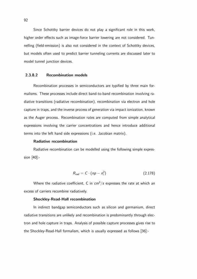
92
Since Schottky barrier devices do not play a significant role in this work,
higher order effects such as image-force barrier lowering are not considered. Tun-
nelling (field-emission) is also not considered in the context of Schottky devices,
but models often used to predict barrier tunneling currents are discussed later to
model tunnel junction devices.
2.3.8.2 Recombination models
Recombination processes in semiconductors are typified by three main for-
malisms. These processes include direct band-to-band recombination involving ra-
diative transitions (radiative recombination), recombination via electron and hole
capture in traps, and the inverse process of generation via impact ionization, known
as the Auger process. Recombination rates are computed from simple analytical
expressions involving the carrier concentrations and hence introduce additional
terms into the left hand side expressions (i.e. Jacobian matrix).
Radiative recombination
Radiative recombination can be modelled using the following simple expres-
sion [40]:-
Rrad = C · (np − n2i ) (2.178)
Where the radiative coefficient, C in cm3/s expresses the rate at which an
excess of carriers recombine radiatively.
Shockley-Read-Hall recombination
In indirect bandgap semiconductors such as silicon and germanium, direct
radiative transitions are unlikely and recombination is predominantly through elec-
tron and hole capture in traps. Analysis of possible capture processes gives rise to
the Shockley-Read-Hall formalism, which is usually expressed as follows [36]:-

93
RSRH =n · p − n2i
τp · (n + n1) + τn · (p + p1)(2.179)
Where n1, p1 are the density of occupied electron and hole traps for a given
temperature, as given by:-
n1 = ni · exp(
Etrap
kT
)
(2.180)
p1 = ni · exp(
−Etrap
kT
)
(2.181)
where Etrap is the energy level of the trap.
In practice, these formulae are difficult to implement in the discretisation
directly, but for low recombination rates it is entirely possible to consider a single
inhomogeneous recombination term. For increasing recombination rates however,
particularly in e.g. Gummel solvers, it is advisable to decouple at least the numer-
ator for inclusion into the LHS (e.g. Fφ, Fn, Fp) to solve for the next iterate.
Additionally, it is important to realise that the lifetimes τn, τp show a strong
dependence on the doping concentration. As such, these lifetimes ought to be
deduced from the bulk lifetime and doping density according to a simple relation,
e.g., that due to Scharfetter [41]:-
τdop(NA,0 + ND,0) = τmin +τmax − τmin
1 +(
NA,0+ND,0
Nref
)γ (2.182)
Auger recombination
Auger recombination can be thought of in general terms as the inverse pro-
cess of impact ionization, discussed in Section 2.3.8.3. Although there are several
possible combinations collectively referred to as Auger processes, the sum total
can be conveniently described by the following model [36]:-

94
RAU =(
CAUn · n + CAU
p · p)
·(
n · p − n2i)
(2.183)
Material Auger coefficient, cm6/s ReferenceElectron Hole
Si 2.8e-31 9.9e-32 [36]Ge 1e-30 1e-30 [42]
CdTe 1e-29 1e-29 [43]
Table 2.4: Typical Auger parameters for materials used in thiswork at T=300K
where CAUn and CAU
p are the Auger coefficients for electrons and holes, re-
spectively. Some nominal values for these parameters for materials of interest in
this work are tabulated in Tab. 2.4.
2.3.8.3 Generation models
Impact Ionization
Impact ionization is the generation of electrons and holes due to collisions
with the lattice. In this work we consider only a fairly simple impact ionization
model, that due to Chynoweth [36]. This basic model should be valid for the fields
of interest (< 1e5 V/cm):-
αn = α∞n · exp
(
−[
E critn
E
]βn)
(2.184)
αp = α∞p · exp
−[
E critp
E
]βp
(2.185)
Optical Generation
Optical generation is modelled using the Beer-Lambert law, which predicts
an exponential fall off of photon concentration with distance through the semicon-

95Material αn E crit
n βn ReferenceSi 1.28e6 2.54e6 1 [36]Ge 1.55e7 1.56e6 1 [36]
Table 2.5: Typical impact ionization parameters for electrons inmaterials used in this work
Material αp E critp βp Reference
Si 1.0e6 2.22e6 1 [36]Ge 1.0e7 1.28e6 1 [36]
Table 2.6: Typical impact ionization parameters for holes in ma-terials used in this work
ductor due to absorption. This expression was first introduced in Section 2.2.2.
Specifically, the generation is given by Eqn. 2.13 and Eqn. 2.14.
Non-local tunnelling Models
Non-local tunneling models are necessary to accurately model transport in
regions of devices such as tunnel diodes, monolithic multi-junction solar cells (with
a tunnel-recombination junction interconnect), Schottky barrier devices and Zener
diodes. The term ”non-local” is used to indicate that the tunnelling process occurs
between mesh points (i.e. at dissimilar points in k-space), rather than between
bands at a single mesh point (or location in k-space).
In this work, we consider the non-local tunnelling model due to Ieong et
al. [44]. Although this model was presented in the context of tunneling currents
through Schottky barriers for use in MOSFET simulations, it is comparatively
straight forward to extend to band-to-band tunneling in bulk pn junction devices,
as is relevant to this work.
The basis of Ieong’s model is as follows. Consider the following expression
(Eqn. 2.186) for the tunneling current density at point v (metal contact) due to

96
Metal
n-type
semiconductor
Figure 2.5: Barrier Tunnelling, after Ieong et al. [44]
electrons tunneling into available states from point u in a Schottky barrier device,
as depicted in Fig. 2.5:-
Jtun = Jtun,M→S − Jtun,S→M
= A∗ · T 2 ·∫ ∞
ǫ
Γ(u) ln
[
1
1 + exp ((ǫ′−EF ,n)/kT)
]
dǫ′−
A∗ · T 2 ·∫ ∞
ǫ
Γ(u) ln
[
1
1 + exp ((ǫ′−EF ,m)/kT)
]
dǫ′ (2.186)
since by Ieong’s arguments, the generation rate due to tunnelling can be
related to the tunnelling current as follows:-
Gtun(u) =dJtun
dǫ· E (2.187)
=A∗ · T
k· E · Γ(u) · ln
[
1 + exp (−(φ−φn)/kT)
1 + exp (−(φ−φm)/kT)
]
(2.188)
where E is the local electric field at point u, Γ(u) is the tunnelling probability
at point u, A∗ is the electron Richardson constant, and k is the Boltzmann con-
stant. The tunnelling probability must be computed by solving the Schroedinger

97
equation in one dimension along the tunnelling path. As in Ieong’s original model,
this can be most easily achieved using a WKB approximation to solve for the
wavevectors required to compute the tunneling path. WKB refers to Wenzel-
Kramers-Brillouin, the originators of this technique, which is most useful for solv-
ing second order differential equations with slowly varying spatial inhomogeneities,
and is particularly applicable to tunnelling problems. The tunnelling probability as
given by the WKB approximation is simply:-
Γ(u) = exp
[
−2
~
∫ u
v
√
(2m∗ (φB + φm − φ))dx
]
(2.189)
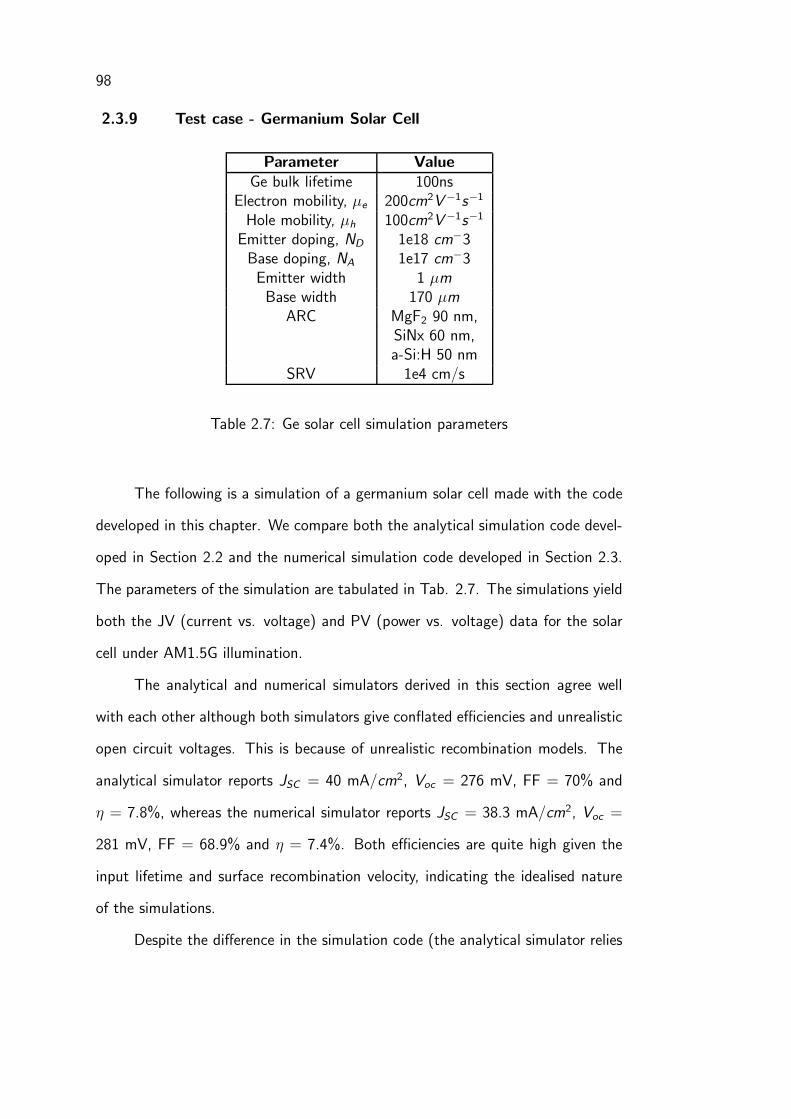
98
2.3.9 Test case - Germanium Solar Cell
Parameter ValueGe bulk lifetime 100ns
Electron mobility, µe 200cm2V−1s−1
Hole mobility, µh 100cm2V−1s−1
Emitter doping, ND 1e18 cm−3Base doping, NA 1e17 cm−3Emitter width 1 µmBase width 170 µm
ARC MgF2 90 nm,SiNx 60 nm,a-Si:H 50 nm
SRV 1e4 cm/s
Table 2.7: Ge solar cell simulation parameters
The following is a simulation of a germanium solar cell made with the code
developed in this chapter. We compare both the analytical simulation code devel-
oped in Section 2.2 and the numerical simulation code developed in Section 2.3.
The parameters of the simulation are tabulated in Tab. 2.7. The simulations yield
both the JV (current vs. voltage) and PV (power vs. voltage) data for the solar
cell under AM1.5G illumination.
The analytical and numerical simulators derived in this section agree well
with each other although both simulators give conflated efficiencies and unrealistic
open circuit voltages. This is because of unrealistic recombination models. The
analytical simulator reports JSC = 40 mA/cm2, Voc = 276 mV, FF = 70% and
η = 7.8%, whereas the numerical simulator reports JSC = 38.3 mA/cm2, Voc =
281 mV, FF = 68.9% and η = 7.4%. Both efficiencies are quite high given the
input lifetime and surface recombination velocity, indicating the idealised nature
of the simulations.
Despite the difference in the simulation code (the analytical simulator relies

99
on closed-form expressions to evaluate the solutions to the drift-diffusion equations,
whereas the numerical simulator solves these equations numerically using a 1D
version of finite element analysis) the results are very similar. The numerical
simulator reports lower short circuit current density. This is due to more realistic
recombination models, for example Shockley-Read-Hall statistics, as opposed to
the pseudo first-order model assumed in deriving the analytical model. However
the difference is negligible. The results confirm and verify both models. The only
noticeable difference between the two simulations is the time taken: the analytical
simulator took one tenth the time to complete. This demonstrates the power of
analytical modelling.
100
2.4 Summary and Conclusions
In this chapter an analytical model for single junction solar cells was ex-
pounded. This involved computation of the dark current, photocurrent and device
parasitics. Analytical models are seen to yield answers more rapidly due to the
analytical nature of output expressions for a given input.
A numerical simulation framework was also developed. This consisted of
discretisation of the drift-diffusion equations, and numerical solution using either
a decoupled or a fully-coupled non-linear solver. The decoupled solver was seen
to outperform the fully-coupled solver since the increased size of the fully coupled
matrix bore a computation time penalty that outweighed the benefit of fewer
iterations.
Finally, comparing both the numerical and analytical simulators, performance
was seen to be similar in the sense that outputs agreed within reasonable limits,
however the analytical simulator was the fastest to yield answers. This makes one
question the need for numerical simulators for back of the envelope computations,
and suggests that analytical calculations are faster and sufficiently accurate to
render more complicated models unnecessary. Although the example given is for
the case of a single junction germanium solar cell under AM1.5G illumination, the
modelling framework developed in this chapter is applicable to all kinds of single
and multi junction solar cell structures.

101
0.00 0.05 0.10 0.15 0.20 0.25 0.30Voltage, V
0
10
20
30
40
50Current, mA/cm−2
Current-Voltage characteristics
AnalyticalNumerical
0.00 0.05 0.10 0.15 0.20 0.25 0.30Voltage, V
0
1
2
3
4
5
6
7
8
Power, mW/cm−2
Power-Voltage characteristics
AnalyticalNumerical
Figure 2.6: Comparison of simulators developed in this chapter

Chapter 3
Device modelling, design and optimisation of tandem II-VI and
germanium solar cells
3.1 Introduction
Thin film photovoltaic (PV) cells have begun to establish themselves as viable
alternatives to the dominant PV technology, crystalline silicon, which is a proven,
robust and efficient technology. At present, commercial thin-film technologies,
comprising cadmium telluride (CdTe), copper indium gallium diselenide (CIGS)
and amorphous silicon (a-Si:H) cannot achieve the peak efficiencies of crystalline
silicon solar modules, but rather are competitive for economical reasons, offering
a lower cost per peak watt to end customers [45].
CdTe solar cells have been previously fabricated using a wide variety of meth-
ods, including ion-implantation [9], molecular beam epitaxy (MBE) [46], close-
spaced sublimation (CSS) [14, 47, 48], spray pyrolysis [8], close-spaced vapour
transport (CSVT) [49], metal-organic chemical vapour deposition (MOCVD) [50,
51], chemical vapour deposition (CVD) [52], and RF-magnetron sputtering [16,
17, 53]. Although in almost all cases CdTe solar cells are a heterojunction formed
between a naturally n-type CdS window layer and a naturally p-type CdTe layer,
homojunctions have also been investigated [9, 52]. It must be noted that the
efficiencies reported thus far for homojunctions (roughly 3-10%) are not compa-
rable with those commonly reported for heterojunctions. There is some evidence

103
to suggest that the CdS layer reduces electron leakage through the junction due
to tunnelling [54], however this alone does not explain the difference between re-
ported results of device efficiency, which could be attributable to a range of issues
including surface recombination, difficulty with doping CdTe, or poor fill factors
relating to difficulties in forming contacts to the devices.
Germanium solar cells have been the subject of some research for application
in thermophotovoltaics [27] and as bottom cells in multijunction solar modules for
space and terrestrial concentrators [55]. Germanium wafers may be doped using
spin-on dopants [21, 22, 27] or gaseous diffusion [56]. Back contact formation
usually consists of deposition of aluminium and annealing above the eutectic tem-
perature [22]. Polycrystalline germanium thin-films have been deposited using
RF-magnetron sputtering [57] and found to have higher absorption coefficients
and optical band gaps. Polycrystalline thin-films are of interest since the combina-
tion of thin-film CdTe and thin-film polycrystalline germanium in tandem promises
a cost effective, highly efficient solar cell [58]. In this section we employ Synopsys
Sentaurus Device to examine such a solar cell structure.
While CdTe thin-film growth on germanium substrates has been the subject
of research as a buffer layer for growth of HgCdTe [24, 29] for infrared detector ap-
plications, very little attention has been given to the electronic (and photovoltaic)
properties of this combination of materials. In contrast, Katnani et al. investigated
overlayers of silicon and germanium on a variety of different substrates (including
CdTe) and determined band offsets by synchrotron-radiation photoemission [59].
From this, the valence band offset of CdTe on germanium was determined to be
0.85 eV. Despite these investigations, the electronic properties of the CdTe/Ge
interface remain relatively unknown.
Although the bandgaps (1.5eV and 0.67eV for CdTe and Ge, respectively)
are not optimal for a two-junction tandem cell [4, 60], the photocurrents are

104
reasonably well matched and simulation has shown that respectable conversion
efficiencies (approaching or exceeding 20%) can be achieved, if the best practi-
cal CdTe and Ge cells are combined in tandem [58].There is perhaps a point of
concern of the performance of the lower band-gap germanium cell at elevated
temperatures; however it must be noted that germanium has performed well in
thermophotovoltaic applications [27] and as the bottom cell of multijunction III-V
concentrator cells [55].
Thin film multijunction solar cells have been investigated previously. For
example, amorphous silicon devices with up to 3 junctions have been presented
with stable conversion efficiencies reaching 13% [61]. Multijunction amorphous
silicon devices are usually a series of stacked p-i-n structures with interconnect
consisting of tunnel-recombination junctions (TRJ) where trap assisted tunnelling
(TAT) and increased recombination rates are employed to allow majority carriers to
recombine and hence exit the sub-cells [62]. On the other hand, Compaan et al.
present an RF-magnetron sputtered CdTe/HgCdTe tandem with a tunnel junction
interconnect consisting of ZnTe:N and ZnO:Al [53]. The interconnect between
series connected monolithic tandem cells is very important to device performance;
high recombination rates at the interface for majority carriers exiting from each
cell are required. To this end, III-V concentrator cells usually rely on band to band
tunneling (BTBT) as the main mechanism for carrier recombination in the TRJ
to accommodate the high current densities required [63, 64].
The monolithic structures presented in this section feature tunnel junctions
which rely on BTBT. It must be conceded that this makes a number of assumptions
about the CdTe/Ge hetero-interface that have not yet been experimentally veri-
fied. For this reason, and to ease the requirements for high doping, an alternative
structure is presented herein which consists of an all germanium tunnelling/re-
combination region, where BTBT can readily be achieved [65]. Device structures

105
relying entirely on TAT in the tunnel junction region are not considered in this
section, as too little is known about the electronic properties of the CdTe/Ge
interface to produce meaningful simulations of this effect.
Simulation has shown that optimisation of the tunnel junction is of crucial
importance to realising high device efficiencies. In particular, minority carrier flow
must be prevented; in III-V concentrator cells, barriers can be imposed to block
minority carrier flow [64], since this is achievable within the III-V material system.
In combining CdTe and Ge, however, such a luxury does not exist, and instead
regions must be doped appropriately (forming front and back surface fields as
appropriate) to reduce minority carrier flow.
Three monolithic tandem cell structures are now considered and their per-
formance evaluated. The first two structures are CdTe homojunctions intended to
be grown by MBE on doped germanium wafers, and differ in their approach to
the tunnel junction. MBE has been chosen as the growth technology due the ease
of growing complex multilayered structures of high quality with good control over
interfaces and dopant incorporation. It must be stressed that MBE is not intended
for the long term development of thin-film tandem cells; but rather intended to
fulfill short term needs to prove the concept and obtain necessary parameters to
improve the accuracy of simulations. Long term, the structure presented in section
3.1.2 is to be pursued which can be fabricated using a combination of chemical
bath deposition (CBD), CSS, and/or sputtering. This structure is intended for low
cost production, and is essentially a thin-film on thin-film tandem solar cell.
Additionally, a mechanically stacked tandem structure is also considered for
completeness to compare the optical matching and device efficiency with the mono-
lithic counterparts. Some advantages of the mechanically stacked configuration
are outlined.

106
Figure 3.1: CdTe homojunction on Ge substrate device structure.Tunnel junction is a heterojunction formed at the CdTe/Ge in-terface.
3.1.1 CdTe homojunction on crystalline germanium substrate
3.1.1.1 Heterostructure tunnel junction
Two approaches to the problem of sub-cell interconnection using a tunnel
diode are under consideration. In the first approach, a tunnel diode is formed at the
heterointerface of CdTe and Ge. In this structure, both materials are very heavily
doped (≥ 2 × 1019 cm−3) in a narrow (∼ 30 nm) region about the metallurgical
junction. Simulation (performed using Synopsys Sentaurus Device) results of the
tunnel junction, where the valence band offset in germanium is taken to be 0.88 eV
[58] and the electron and hole effective masses are 0.08 and 0.117 m0 respectively,
are depicted in Fig. 3.2 [58]. It is evident that the junction is more than capable
of allowing sufficient majority carrier flow (recombination of majority carriers in
the vicinity of the metallurgical junction) by tunnelling to support functional cells,

107
0.00 0.02 0.04 0.06 0.08 0.10 0.12 0.14 0.16Bias, Volts
0
200
400
600
800
1000
1200
1400
Curr
ent
Densi
ty, J, mA/cm
2
Figure 3.2: CdTe/Ge heterojunction tunnel diode current-voltagecharacteristics. Peak tunneling current density more than satis-fies the requirements for cells operating under 1 sun illumination(≃ 26mA/cm−2) [58].
Parameter Description Valueµe,CdTe CdTe electron mobility 1260 cm2/Vs [2]µh,CdTe CdTe hole mobility 104 cm2/Vs [2]Eg,CdTe CdTe band gap 1.5 eV [2]χ0,CdTe CdTe electron affinity 4.05 eV [58]τSRH,CdTe CdTe SRH lifetime 1 ns [66]µe,Ge Ge electron mobility 3800 cm2/Vs [67]µh,Ge Ge hole mobility 1800 cm2/Vs [67]Eg,Ge Ge band gap 0.67 eV [42]χ0,Ge Ge electron affinity 4.0 eV [58]τSRH,Ge Ge SRH lifetime 1 ms [42]
Table 3.1: Simulation parameters for crystalline CdTe homojunc-tions on crystalline Ge substrates
since the peak tunneling current density (≃ 1200 mA/cm−2) is much greater than
the device short circuit current density (≃ 24− 26 mA/cm−2).
The full device structure and energy band diagram are presented in Fig.

108
Figure 3.3: Proposed energy band diagram for a CdTe homo-junction on Ge substrate. Note desirable overlap of valence andconduction bands in the tunnelling / recombination junction.Not to scale.
Ge FSF doping Ge emitter doping Jsc (mA/cm2) η3e19 cm−3 3e17 cm−3 25.60 19.76 %3e19 cm−3 2e18 cm−3 25.54 19.75 %4e19 cm−3 3e17 cm−3 25.63 20.09 %5e19 cm−3 3e17 cm−3 25.68 20.32 %5e19 cm−3 2e18 cm−3 25.66 20.31 %
Table 3.2: Efficiency vs. Ge FSF/emitter doping, under 1-sun,AM1.5G illumination. Note efficiency improvement with increas-ing front surface field (FSF:n+germanium tunnel diode region)doping.
3.1 and Fig. 3.3, respectively. The device is modelled using optical databases
109
(n and k values) from Tousek [68] for CdTe and Palik [69] for Ge. Minority
carrier lifetimes are set to 1 ns [66] and 1 ms [42] for CdTe and germanium
respectively. Front and back surface recombination velocities are set to 5e5 cm/s
and 1e3 cm/s [58], respectively. Surface recombination at the interface is set
to 1e2 cm/s; however simulation results are relatively insensitive to the value
assumed (since recombination in the tunnel junction is desirable). Simulation
takes into account band gap narrowing and doping dependent mobility in the
germanium cell. The doping dependent mobility data is from Palankovski [67].
Such effects are neglected for the CdTe cell, due to a lack of experimental data.
Incomplete ionization is also included. TAT is simulated using the Hurkx model
[41]. Simulation parameters for this cell are given in Tab. 3.1.
As noted above, simulation has shown that majority carrier flow across the
tunnel junction is also possible and this imposes limits on ultimate device efficiency.
Electron flow from the CdTe absorber region to the Ge emitter is negligible; this
is owing to the tunnel junction p+ region acting as a back surface field (BSF).
The same cannot be said for hole flow from the Ge emitter to the CdTe absorber;
however, this may be mitigated by reducing the Ge emitter doping and doping
the tunnel diode n+ region more heavily, producing a front surface field (FSF).
The emitter doping ought not to be reduced too drastically, as this will result in
lower open circuit voltage for the lower cell (and hence the tandem structure). By
reducing minority carrier flow accross the tunnel diode we may make some gains
on open circuit voltage due to reduced recombination but there will inevitably be
a cross over point where any potential advantages are out weighed by diminishing
bottom cell Voc . Results of overall cell efficiency vs. tunnel junction n+ region
doping are presented in Tab. 3.2 for devices with a 2.5 µm thick CdTe absorber
layer and a 15 µm thick Ge absorber layer. The device structure is simulated under
1 sun, AM1.5G illumination.

110
0.4 0.6 0.8 1.0 1.2 1.4 1.6 1.8Wavelength, m
0.2
0.0
0.2
0.4
0.6
0.8
1.0a.u
EQE and Reflection
EQE CdTeEQE GeReflection
Figure 3.4: CdTe homojunction on Ge substrate: external quan-tum efficiency and reflectance plot versus wavelength. Note thereflection losses caused at the CdTe/Ge interface. Data obtainedfrom Sentaurus simulation using transmission matrix method.
Although the heterostructure tunnel junction performs well in simulation,
there are definite concerns about physical realizability, since p type doping of CdTe
to the levels required is non-trivial. Although hole concentrations of 5× 10¹⁹ have
been reported using ion-implantation and pulsed electron beam annealing [70], ion
implantation is not particularly amenable to commercial manufacture of large-scale
modules. Nevertheless, this approach can be used as a starting point to investigate
whether or not such a structure can be physically realised.
Optical modelling using the transfer matrix method (TMM) shows significant

111
reflection at the interface. The external quantum efficiency (EQE) and reflectance
plot for the two cells of the tandem is shown in Fig. 3.4 as a function of wavelength.
The optical losses at the CdTe/Ge interface, combined with the non-idealities of
the tunnel junction, present difficulties in matching photocurrents between the two
cells of the tandem. Note that the the bi-layer antireflection coating of the device
structure consists of 60 nm of TiOx covered by 100 nm of MgF2 and serves to
minimize reflection losses at the front surface.
3.1.1.2 All germanium tunnel junction
In order to relax the doping requirements for p-type CdTe somewhat, and cir-
cumvent the problem of potentially unfavourable band alignment at the CdTe/Ge
interface, an alternative structure is presented in Fig. 3.5, which features a tunnel
diode realised entirely in germanium. The energy band diagram for this structure
is depicted in Fig. 3.6. This is the second approach to the problem of intercon-
nection of the two tandem cells. In this configuration, the underlying Ge substrate
wholly contains the tunnel diode which is defined using e.g. spin on diffusants.
In order to improve majority carrier injection while reducing minority carrier flow
across the heterointerface, a back surface field is realised in the CdTe absorber.
The doping density required for the back surface field is considerably less than for
the above heterojunction tunnel diode p+ region. Results are presented in Tab.
3.3.
The disadvantages of this structure are the limitations imposed on the doped
substrate in terms of high temperature processing. For example, it is usual during
MBE growth on Ge to outgas the native oxide at 650C [24] which would cause
significant diffusion of the dopants in the germanium substrate [22]. The time for
oxide outgassing therefore must be kept to a minimum.
Another disadvantage is that there is now a p+-CdTe / p+-Ge region formed,

112
Figure 3.5: CdTe homojunction on Ge substrate featuring all-germanium tunnel junction. Tunnel diode is formed entirelywithin the underlying germanium substrate.
CdTe BSF doping Jsc (mA/cm2) FF η2e18 cm−3 24.74 74.06 % 19.48 %3e18 cm−3 24.74 77.9 % 20.43 %6e18 cm−3 24.74 78.2 % 20.47 %
Table 3.3: Efficiency vs. CdTe BSF doping for structure withall-Ge tunnel diode under 1 sun, AM1.5G illumination. Notethe efficiency improvement with increasing BSF doping. Theshort circuit current density is limited by the germanium bottomcell and hence is unaffected by CdTe BSF doping. This can beimproved slightly by optimising CdTe thickness, see Tab. 3.5.
and interdiffusion of dopants from either side of this junction will cause parasitic
doping which will affect the net doping of each region detrimentally (for example
Sb is a p-type dopant in CdTe but an n-type dopant in Ge).

113
Figure 3.6: Proposed energy band diagram for all-Ge-TRJ con-taining structure
Parameter Description Valueµe,CdTe CdTe electron mobility 320 cm2/Vs [?]µh,CdTe CdTe hole mobility 40 cm2/Vs [?]Eg,CdTe CdTe band gap 1.5 eV [?]τSRH,CdTe CdTe SRH lifetime 1 ns [66]µe,Ge Ge electron mobility 350 cm2/Vsµh,Ge Ge hole mobility 150 cm2/VsEg,Ge Ge band gap 0.88 eV [57]τSRH,Ge Ge SRH lifetime 1 µs
Table 3.4: Simulation parameters for thin film CdS/poly-CdTe/poly-Ge heterostructures
3.1.2 Conventional CdTe heterojunction
Unlike the previous structures, which are intended to serve as proof of con-
cept cells to be grown on single crystal germanium substrates by MBE, in this

114
Figure 3.7: CdS/CdTe/Ge tandem solar cell structure. 100 nmthick MgF2 is deposited on the glass front surface as an anti-reflection coating.
CdTe absorber Jsc FF Voc ηwidth (µm) (mA/cm2) (Volts)
0.5 22.66 78.06 % 1.088 19.24 %0.6 23.52 76.76 % 1.08 19.51 %0.8 24.29 74.14 % 1.078 19.28 %
Table 3.5: CdS/CdTe/Ge tandem cell simulation results. Notethe optimum CdTe absorber width.
structure, a CdS/CdTe heterojunction cell is to be first deposited on ITO glass,
with a MgF2 antireflection coating, as usually found in the literature [48, 14].
The polycrystalline germanium cell is then to be formed using a low-temperature
deposition process, e.g. sputtering. The layers must be doped appropriately to
realise the tunnel junction and emitter/absorber regions. The structure is depicted
in Fig. 3.7 and its energy band diagram in Fig. 3.8.
In order to model polycrystalline germanium, the band gap, mobility, minority

115
Figure 3.8: Proposed energy band diagram for conventional CdTeheterojunction thin film tandem cell
carrier lifetimes and optical database are modified accordingly. The n and k values
were taken from Tsao [71] and the electron mobilities were set to 350 and 150
cm2/Vs, respectively, in order to be indicative of polycrystalline material [72].
Likewise, lifetimes were set to 1 µs. These figures were chosen as being plausible
in the context of the literature. Simulation parameters are summarized in Tab.
3.4.
Simulation results are presented in Tab. 3.5. The Ge tunnel diode n+ region
doping was set to 3e19 cm−3 and the Ge emitter doping was set to 2e18 cm−3.

116
The width of the Ge absorber was set to 20 µm. Incomplete ionization, doping
dependent mobility, bandgap narrowing and TAT were taken into account.
It must be noted that the optimal CdTe absorber width as shown in Tab 3.5
is only 0.6 µm, which is significantly less than normally deposited for commercial
CdTe solar cells [73]. If this is a realistic value, then this would be of advantage
in manufacture, requiring less scarce tellurium per module.
On the other hand, simulation has shown that thicker germanium films are
required than first anticipated [58]. Around 20 µm is required to optimize device
performance by attempting to better match photocurrents. Beyond this value,
negligible improvement in device efficiency results.
3.2 Mechanically stacked tandem solar cell
We now examine the potential for a mechanically stacked CdTe/Ge tandem
solar cell. This structure has a few potential advantages over the three monolithic
structures already discussed. Firstly, the device may be bonded in a four wire con-
figuration. In this configuration, both cells are independently bonded and there
is no interconnect between cells. This has the advantage that photocurrents do
not need to be matched, and there is no tunnelling/recombination junction which,
as we have seen, is problematic in the case of CdTe and Ge. Secondly, optical
matching between the CdTe and Ge may be better achieved since the device is no
longer monolithic and A/R interlayers are now feasible. One example of such a
structure is CdTe on sapphire, which is almost refractive index matched to silicon
nitride (SiNx). If CdTe is grown on sapphire and mechanically stacked with a
germanium subcell coated in a SiNx based A/R coating, we would conjecture that
the reflection losses at the interface could potentially be reduced in comparison to
the monolithic case. The third advantage is that we overcome some of the limita-
tions of the materials science of CdTe and Ge by separating the substrates. CdTe

117
and Ge can now be processed independently at elevated temperatures without any
detrimental affect on one another and without risk of alloy formation. Also, we
now have flexibility in the choice of sub-/super- strate for CdTe deposition, and
can choose a material with more favourable material properties, such as lattice
constant.
Disadvantages of the mechanically stacked tandem include higher processing
costs due to added complexity, and more complicated interconnect, especially in
the case of a four-wire connected tandem. However, with difficult materials such
as CdTe and Ge, these disadvantages may be outweighed by the benefits gained
from separating the two cells mechanically.
Front contacts
Rear contacts
Figure 3.9: Diagram of proposed mechanically stacked tandemstructure
The proposed mechanically stacked tandem structure is depicted in Fig. 3.9.
The main features are the CdTe heterojunction solar cell deposited on sapphire,
with buried contacts to the CdTe layer bought out to the front surface, and an
aluminium doped zinc oxide (AZO) transparent conducting oxide. AZO is chosen
due to better infrared transparency than indium tin oxide (ITO). The germanium

118
cell is a back-junction design with contacts to the device protruding from the rear
surface. This allows for a flat interface between the sapphire surface and the SiNx
passivation/AR layer, so there is no air gap. In fact the two cells could be adhered
to one another using some kind of wafer bonding process, however what impact
that would have on each subcell is not known.
0 500 1000 1500 2000Wavelength, nm
0
20
40
60
80
100
Transm
ission / reflectance (%)
Transmission / reflectance for mechanically stacked tandem solar cell
TR
Figure 3.10: Reflectance and transmission at the Ge cell emittersurface for structure of Fig. 3.9
The optical transmission and reflectance at the Ge bottom cell emitter is
shown in Fig. 3.10. When compared with Fig. 3.4, the reflectance is not sig-
nificantly better, weakening our argument that the mechanically stacked tandem
should have better optical performance. The interference is mostly due to the
interface of the sapphire substrate/SiNx layer and is due to slight refractive index
mismatch. Experimental tuning of the SiNx layer thickness did not yield significant
performance gains. The best course of action to obtain a better match would be
SiNx refractive index tuning. This is discussed in Chapter 5.
Simulation results for the lower cell in the stacked (which can be simulated
independently in the case of a mechanically stacked tandem) are tabulated in Tab.
3.6. Since photocurrents no longer need to be matched, the CdTe can be assumed

119Sun Jsc FF Voc η
(mA/cm2) (Volts)1 22.6 72.16 % 0.310 5.03 %100 2,260 77.28 % 0.425 7.47 %
Table 3.6: Simulation results for Ge bottom cell of mechanicallystacked tandem
to be at least 5 µm thick meaning that the top cell can be optimised to absorb
almost all radiation above the energy gap of CdTe. This means that energy can
be most efficiently converted in the top cell leaving only the unabsorbed photons
to permeate to the lower cell. This highlights the advantage of a mechanically
stacked configuration with four-wire interconnect. Simulation shows that the Ge
bottom cell could add 5.03% efficiency in this configuration for 1 sun illumination
and 7.47% for 100× concentration. Since the device is 4-wire connected, the
efficiencies simply add. If the top CdTe cell could be made as efficient as leading
CdTe solar cells of today, i.e. 21.5% efficient, the total efficiency would be 26.5%
at 1 sun. This would be a very promising photovoltaic device indeed.
3.3 Conclusion
A novel thin film tandem device, consisting of the combination of thin film
cadmium telluride with either crystalline or polycrystalline germanium, has been
modelled and simulated in Synopsys Sentaurus Device. Three such monolithic
structures have been considered. It has been shown that device efficiencies ap-
proaching or exceeding 20% are achievable assuming a nominally 15-16% efficient
CdTe top cell. An alternative structure, whereby the tunnel junction is realised
entirely in germanium, thus relaxing the constraints for extremely high p-type dop-
ing concentrations in CdTe, has been considered, and has been shown to function
adequately. It must be noted that the doping concentrations required to form
120
a BSF capable of achieving high efficiencies are still quite difficult to achieve in
CdTe, even under idealised circumstances.
A more commerically feasible structure, a CdS/CdTe heterojunction with a
polycrystalline germanium bottom cell, was also considered, and performed quite
well in simulation, in spite of poorer lifetimes and mobilities chosen to be indicative
of polycrystalline material. It is assumed that such a structure can be fabricated
using CSS or sputtering on glass superstrates, essentially fabricated from the top
down. This is in contrast to the first two structures proposed herein, which are
to be constructed from the bottom up by deposition of material on crystalline
germanium substrates.
Finally, a mechanically stacked tandem structure was investigated. This
offers the advantage of easing the requirements for photocurrent matching, allevi-
ating the difficulties of materials processing, particularly for high temperature pro-
cessing, and potentially improving optical matching and reducing reflection losses.
In practice, the structure considered in this section did not significantly improve
optical losses but did deliver a more efficient lower cell. At 100× concentration
ratio, as much as 7.47% efficiency could be achieved for the lower cell, boosting
the efficiency of a standalone CdTe cell. This requires specialised processing of
CdTe solar cells, and in particular inverting the structure to realise it in substrate
rather than superstrate configuration. Nevertheless, the mechanically stacked tan-
dem structure promises a great deal for the case when monolithic structures are
deemed unrealisable due to difficult material properties.

Chapter 4
Low-cost techniques for germanium device active region formation
4.1 Introduction
In this chapter we present some low cost methods for germanium pn-junction
device active region formation. These techniques allow one to form the crucial
device region, the pn-junction itself, in a low cost manner and most importantly,
in a manner amenable to mass-manufacture. We consider the use of spin-on
dopants to introduce impurities into the device regions for junction formation. We
present, in addition to the more conventional spin-on technique, a comparison of
both “proximity doping”, a variation of doping from solid sources, and “sandwich-
stacked diffusion”, a novel technique to introduce the impurities from a spin-on
source.
4.2 Spin-on dopants
Spin-on dopants are predominantly silica based solutions that can be spun
onto a wafer and outgassed to form a uniform dopant impregnated layer to act as
a diffusion source. The dopant products can be obtained from a variety of manu-
facturers or created in-house using sol-gel techniques. For example, spin on glass
can be manufactured using TEOS (tetra-ethyl orthosilicate), water, isopropanol,
and hydrochloric acid [74]. The result is a transparent, thin solution of solvents
and embedded silica nanoparticles, following the polymerisation of silica during the

122
reaction. By adding into the mix a proportion of dopant material, the solution will
contain a certain amount of dopant and will be able to act as a diffusion source
when spun onto a wafer.
4.3 Degenerate p-type doping and sandwich stacked diffusion
1. Si wafer spin
coated with
spin-on dopant
film
("Source Wafer")
2. dopant
"source"
wafer out-
gassed
at 100 - 200 Deg. C
in cold end of furnace
3. "Sandwich" diffusion
stack assembled
Silicon wafer: back-side diffusion barrier
Germanium"Target wafer"
Silicon"Source wafer" Spin-on
dopant film
4. "Sandwich"
diffusion
stack
loaded into
quartz boat
for
introduction
into furnace
("pre-dep")
Figure 4.1: “Sandwich-stacked diffusion”
In this section, we explore the use of Ga doping of Ge using a novel technique
- “sandwich-stacked diffusion” - which yields doping densities ≫ 5 × 1019 cm−3
with the potential for shallow junctions, and which is amenable to rapid thermal
processing (RTP). This process is depicted in Fig. 4.1.
We note that the sandwich-stacked diffusion method differs from proximity
doping [75] by the fact that the sol-gel film (as spin coated on the silicon dopant
source wafer) is in physical contact with the target wafer (in this case, a piece of
123
Ge). The sandwich-stacked method has the advantage of providing better control
of diffusion into Ge of impurities which do not have high vapour pressure at the
diffusion temperature, e.g. Ga and its oxides.
Gallium is a particularly suitable dopant for degenerate doping of Ge by
solid-state diffusion due to reasonable diffusivity, high solubility (> 1020 cm−3)
and natural affinity for Ge. This is in contrast to B which displays very high
activation energies [76, 77] and lower solubility [77]. Gallium diffusion in Ge has
been investigated by diffusion from solid sources in sealed ampoules [76] and from
ion implantation [78]. Solid state diffusion of Ga into Ge from spin-on dopants
(SODs), however, appears to be a fairly novel concept.
In this work, we present this novel technique and employ it to degenerately
dope n and p-type Ge wafers. Sheet resistance and SIMS profiling are used to
characterise the dopant profile, from which thermal activation energies and pre-
exponential factors are extracted, and a simple analytical model is proposed for the
post-“drive-in” profile. It is envisaged that this technique can be applied in a range
of electronic and optoelectronic applications, in particular for use in back-surface
fields for multijunction photovoltaic cells.
4.4 Experimental
4.4.1 Sample preparation
A 2” p-type Ga doped (3.3 Ω · cm, 1× 1015 cm−3) Ge wafer purchased
from University Wafer [Boston, MA, USA] and a 3” n-type Antimony doped
(40 Ω · cm,∼ 1× 1014 cm−3) Ge wafer purchased from Umicore [Olen, Belgium]
were diced into 1cm × 1cm samples and cleaned in a 3 step solvent clean. This
consisted of 3 min. in each of boiling trichloroethylene, acetone, and methanol,
followed by 1 minute of ultrasonic cleaning after each step, to remove fine Ge

124
Samples Supplier Conductivity type Resistivity (Ω · cm)
GE219:1-4 University Wafer p-type 3.3
GE220:1-4 Umicore n-type 40
Table 4.1: Sample summary
particles left by the cleaving process. The samples were labeled as documented in
Tab. 4.1.
These samples were then cleaned in 1:1:20 NH4OH :H2O2 :DI water for 30s
to etch ∼ 100nm of the surface, followed by a 1 min. soak in 1:1:3 HCl:HBr :DI
to strip any surface oxide and passivate the surface. This passivation process is
known to be relatively air-stable [79, 80].
Silicon wafers were cleaved into 1cm × 1cm squares and cleaned using the
standard RCA cleaning procedure. Half the Si squares were then spin-coated with
Ga/B spin-on dopant solution GaB 260 from Filmtronics [Butler, PA, USA]. The
dopant films are not spun onto the Ge directly, since after diffusion HF insoluble
films form [81] which cannot easily be removed without damage to the Ge itself,
due to the high chemical reactivity of Ge.
The Si and Ge samples were packaged and labelled ready for diffusion in a
horizontal 2” tube furnace. First the Si dopant source wafers were loaded into the
quartz boat and outgassed in the cool part of the furnace tube at 100 - 200C to
cure the dopant film and drive off organic solvents and other contaminants within
the film [82, 83].
4.4.2 Sandwich-stacked diffusion
To diffuse the dopant into the Ge, a sandwich-stack is formed with the
dopant source at the bottom, covered by the target Ge wafer, which is then itself

125
covered by a spare piece of clean silicon wafer, to prevent unintentional diffusion
from volatile dopant compounds and impurities, e.g. B, which was present in the
GaB spin-on dopant film. This is depicted in Fig. 4.1.
The samples were diffused in flowing nitrogen ambient, with high gas flow
(10 L/min). This removes any residual, volatile organic contaminants from the
sample, which are present in the sol-gel dopant films. High nitrogen gas flow
also prevents oxidation of the sensitive germanium (which oxidizes quite rapidly at
elevated temperatures).
Samples were loaded into the quartz boat and introduced into the furnace.
After diffusion, the samples must not be retracted rapidly; i.e. air quenched, as this
will introduce defects, particularly in the low doped n-type wafers, in which defects
can even introduce type conversion to p-type [84]. To alleviate this problem, the
sample is left inside the furnace tube and the furnace is switched off, allowing it
to cool. The time constant for cooling (defined as time for temperature to decay
to 63% of the final value) is discussed below; the average cooling rate is roughly
2 C/minute from 800 C.
Due to the low diffusivity of all acceptors in Ge, practical constraints place
700C as a lower bound on the diffusion temperature, since below this temperature
no appreciable diffusion will occur, even after several hours. Above 850C, the
crystallinity of the Ge will be severely compromised introducing a great many
defects. Hence, a practical diffusion temperatures lie in the range of be 750 - 800
C.
The heating and cooling dynamics of the sample need to be accounted for
when characterising the diffusion process. Firstly, the quartz boat and the quartz
rod handle will limit the maximum heating rate of the sample. Secondly, cooling
under gas flow, which has a non-negligible time constant, effectively prolongs the
diffusion. In order to derive a time-dependent model for heating within the furnace,

126
Process time constant (s)
Sample cool down 3529
Sample rise time 48
Table 4.2: Furnace time constants, defined as time taken toreach 63% of the final value
Sample Nominal Time (s) Temp. Eff. time (s) Eff.
set point (C ) temp. (C )
GE0219:2 1380 845 1143 845
GE0219:3 600 866 362 865
GE0219:4 2400 880 2160 880
Table 4.3: Effective drive in times and temperatures for samplesGE0219:2-4.
these two time constants needed to be extracted. To obtain the approximate rise
time within the boat, a quartz rod of the same dimensions (500mm length ×
10mm OD) with quad 1mm bore holes was threaded with a k-type thermocouple.
This was then introduced into the furnace. The thermocouple voltage was sampled
at 1 Hz with a digital multimeter with GPIB attachment and recorded on a PC.
When the temperature had settled to the set-point, the furnace was then switched
off. The respective time constants are tabulated in Tab. 4.2.
The samples in this work were annealed as follows. First, the sandwich-stack
was prepared and introduced into the furnace for the “pre-dep” step. In this step,
a small amount of dopant is diffused to create a heavily doped region with a high
surface concentration of dopant. This can be carried out at lower temperatures to
coat the surface, with the effect that there is minimal diffusion into the bulk. Each
matching pair (e.g. GE0219:1 with GE0220:1 etc.) is pre-deposited simultaneously

127
Sample Eff. time (s) Eff. temp. (C )
GE0219:1 124 749
GE0219:2 360 700
GE0219:3 360 762
GE0219:4 120 772
Table 4.4: Effective predep times and temperatures for samplesGE0219:1-4.
at temperatures ranging from 700 - 800 C.
Then the Si dopant wafer is removed from the stack and each matching
pair of Ge wafers is then sandwiched together, so that the doped regions touch.
This is intended to prevent out-diffusion of dopant. However, as discussed in this
work, n-type 〈211〉 and p-type 〈100〉 wafers have slightly different diffusivities at
a given temperature, so some degree of out-diffusion will still occur. By plotting
the temperature profile using the time constants extracted above, we can estimate
an average temperature and time for use in fitting analytical models to extract
diffusivities and construct the Arrhenius plots necessary to extract the thermal
activation energy and pre-exponential factors, which are necessary to characterise
the diffusion process. We do so by computing the time that the diffusivity (from
D ≃ exp(− 3kT
)) is above 90% of its final value, and computing the average
temperature over this period. Note that an activation energy of 3 eV is taken
from the literature [76]. These effective drive in times and temperatures, based
on the nominal times and the temperature set point, are summarized in Tab. 4.3.
Predep effective times and temperatures are shown in Tab. 4.4.
Samples GE0219:1 and GE0220:1 were not subjected to a drive-in step, and
instead were used to characterise the dose in-diffused during the “pre-dep” step.

128
Sample Sheet Resistance (Ω/2)
GE0219:1 113
GE0219:2 12.4
GE0219:3 11.7
GE0219:4 6.5
Table 4.5: Extracted sheet resistances of GE0219 after drive-in
4.5 Characterisation
The samples were then characterised by measuring sheet resistances and
performing secondary ion mass spectroscopy (SIMS) profiling. From these two
techniques, and assuming complete ionization of acceptors, it is possible to recon-
struct the depth profile and fit a model according to diffusion theory.
4.5.1 Sheet resistance measurements
Sheet resistances were measured using a four-point probe and voltmeter to
measure the sample using a four-wire (Kelvin) measurement. The sheet resistance
is given by the correction factor [85]:-
Rsh =π
ln(2)R4W =
ρ
t(4.1)
where Rsh is the sheet resistance, R4W is the four wire resistance, ρ is the
resistivity, and t is the thickness. The sheet resistances for GE0219 are summarized
in Tab. 4.5. For the case of GE220, however, the sheet resistances were measured
both before and after the drive-in step. These are tabulated in Tab. 4.6.
Under the assumption of complete ionization for dopants, we can calibrate
the SIMS secondary ion yield, as presented in the following section, by using the

129
Sample Sheet Resistance after pre-dep after drive-in
(Ω/2) (Ω/2)
GE0220:1 172.14 -
GE0220:2 135.9 19.5
GE0220:3 36 14.4
GE0220:4 52 5.9
Table 4.6: Sheet resistances of GE0220
following relationship [85]:-
σsh = q
∫ t
0
(µn(n)n(x) + µp(p)p(x)) dx =1
Rsh
(4.2)
For the n-type wafers (samples 220:1-4), this process would be relatively
straight forward, since we may assume in this case we have a high quality p-on-n
junction with minimal injection into the underlying n-type layer. However, for the
p-type wafers (samples 219:1-4) we must first extract the sheet resistance of the
heavily doped region by assuming a simple model of two resistances in parallel.
From this, we can compute the sheet resistance of the doped layer, and then
normalize the SIMS profiles accordingly. We do this as follows:-
Rsh =1
1
R2−
1
R1
(4.3)
where R1 is the measured sheet resistance before and R2 is the measured
sheet resistance after diffusion. Note that some error will be introduced by this
method but it is assumed this will not produce any noticeable effect on the carrier
concentration.
130
We cannot simply scale the SIMS secondary ion yield in proportion to the
quotient of the measured Rsh and the computed sheet resistance from Eqn. 4.2,
since the doping dependence of the mobilities in this integral are non-linear. In-
stead, we use an iterative procedure, where we initialize the scale constant α to
some value, e.g. 1014 counts−1 · cm−3. Then the sheet resistance (Rsh,comp.)
is computed and compared to Rsh. If the absolute value is greater than some
threshold, e.g, if the following relation is not satisfied:-
|Rsh,comp. − Rsh| < ǫ (4.4)
where ǫ may be a few milliohms, then the scale parameter α is adjusted as
follows:-
αn+1 = αn
(
1 + log
(
Rsh,comp.
Rsh
))
(4.5)
The process is then repeated until Eqn. 4.4 is satisfied. This iterative
procedure was found to rapidly converge to a suitable scale constant α yielding
consistency between SIMS depth profiles and sheet resistance measurements.
4.5.2 SIMS profiling
Samples GE0219:1-4 were sent to the National University of Singapore, Sur-
face Sciences Laboratory, for SIMS profiling. Profiling was performed using positive
SIMS using a Cameca IMS6f with a O2+ primary beam at 12.5keV. The raster
area was 250 × 250µm2 . The data was first analysed with a high sputtering rate,
≃ 140 nm/min, and then again with a lower sputtering rate to analyze impurity
content (Fe, B). Interestingly, B was only found at the surface of the samples,
although it is present in equal quantities within the spin-on diffusant film as the

131
Ga impurity (2%). It is evident that B does not easily diffuse at the temperatures
involved. Early studies noted that B does not easily “alloy” with Ge [76], and more
recent studies have called into question previously held results about B diffusion
in Ge [77], which was traditionally held to be a vacancy mediated process. In
fact, results concerning radiation-enhanced diffusivity of B and self-diffusion of Ge
in Ge [86] tend to suggest that B diffusion is in fact due to self-interstitials, the
concentration of which would be quite low at the temperatures investigated in this
work.
In contrast, the Fe content was more pronounced and was seen to diffuse in
one case as far as 300nm into the sample. This Fe is most likely from trace metal
content of the dopant films themselves, and has been noted previously [82].
4.6 Analysis
4.6.1 Fitting procedure to extract diffusivities
Diffusion can be analysed by means of Fick’s second law [87]:-
∂N
∂t= D
∂2N
∂x2(4.6)
where D is the diffusivity of the material, x , t are position (in 1 dimension)
and time, respectively, and N is the concentration of the impurity at x at time t.
For a diffusion from an infinite source with surface concentration of N0 we
have the following well known solution [87]:-
N(x , t) = N0erfc
(
x
2√Dt
)
(4.7)
Whereas if the surface concentration is effectively a delta function, we have
the following solution (constant total dopant problem) [87]:-

132
N(x , t) =Q0√πDt
exp
(−x2
4Dt
)
(4.8)
where Q0 is the total dose at the surface.
In practice neither model is adequate to describe the process discussed in
this work and in fact both models can be fitted to Fig. 4.2. This can be attributed
to the surface deposited layer of Ga compounds (e.g. GaO) or Ga:Ge alloy (which
is evident for example in the SIMS profile of sample GE0219:1) which continues
to supply dopant during the drive-in step, and to out-diffusion between the two
samples of the sandwich-stack during drive-in. Furthermore, the temperature is
not constant throughout diffusion due to heating and cooling effects of the quartz
boat etc.
Since these effects are difficult to account for, we first assume a constant
average temperature and effective diffusion time as computed in Section 4.4.2,
and fit both erfc and Gaussian profiles. Interestingly, the erfc profile provides a
better fit to the tail of the diffusion, whereas the Gaussian profile better accounts
for the first diffusion length of the profile.
The parameters extracted from the model fits are tabulated in Tab. 4.7.
Sample 1 differs from the other samples in that the profile is that of the predepo-
sition step (this sample was not driven-in). In this profile, we see a surface delta
of Ga rich material, which is a residue from the predeposition step, and a shallow
diffused region (∼ 80nm depth).
The three remaining samples were driven-in at higher temperatures for longer
times, in order to tune the surface concentration and extract the model for the
profile, and hence follow a more reproducible pattern. The profile for the region
0 ≤ x ≤ 2√Dt, where 2
√Dt is the diffusion length, is described best by a
Gaussian fit with a slightly lower diffusivity than the tail of the diffusion, which
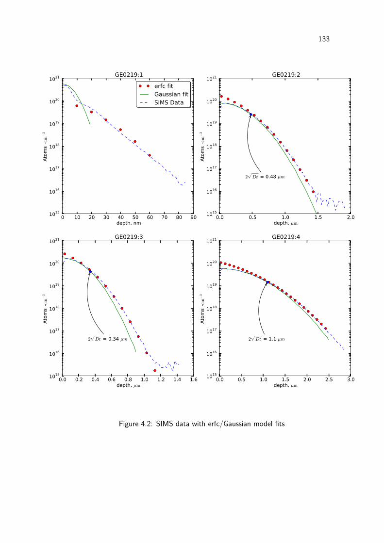
133
0 10 20 30 40 50 60 70 80 90 depth, nm
1015
1016
1017
1018
1019
1020
1021
Atoms ·cm
−3
GE0219:1
erfc fitGaussian fitSIMS Data
0.0 0.5 1.0 1.5 2.0 depth, µm
1015
1016
1017
1018
1019
1020
1021
Atoms ·cm
−3
2√Dt = 0.48 µm
GE0219:2
0.0 0.2 0.4 0.6 0.8 1.0 1.2 1.4 1.6 depth, µm
1015
1016
1017
1018
1019
1020
1021
Atoms ·cm
−3
2√Dt = 0.34 µm
GE0219:3
0.0 0.5 1.0 1.5 2.0 2.5 3.0 depth, µm
1015
1016
1017
1018
1019
1020
1021
Atoms ·cm
−3
2√Dt = 1.1 µm
GE0219:4
Figure 4.2: SIMS data with erfc/Gaussian model fits

134
fits very well to an erfc profile with higher (1.2 - 1.4 ×) diffusivity.
We therefore propose the following simple analytical model to describe dop-
ing profiles from diffusion using this method:-
NGa(x , t) ≃
Q0√π0.8Dt
exp(
−x2
3.2Dt
)
x ≪ 2√Dt
N0erfc(
x
2√Dt
)
x ≫ 2√Dt
(4.9)
where the dose, Q0, is set to remove the discontinuity at x = 2√Dt:-
N0erfc(1) =Q0√π0.8Dt
exp
(
− 1
0.8
)
(4.10)
⇒ Q0 ≃ 0.77× 2√DtN0√π
(4.11)
and N0, the effective surface concentration, is roughly (1 − 3)×1020 cm−3
depending on time and temperature.
In order to extract corresponding parameters for the n-type wafers (sample
GE0220), we fit the model presented in Eqn. 4.9 to the sheet resistance values after
drive-in, and a simple erfc model to the values of the sheet resistance measured
before drive-in, as given in Tab. 4.6. The fitting parameters are summarized in
Tab. 4.8.
4.6.2 Thermal activation energy and pre-exponential factor extrac-
tion
An Arrhenius plot of the data presented in Section 4.6.1 is shown in Fig. 4.3.
The uncertainty in temperature measurement is assumed to be ± 10 C, and the
uncertainty in the extracted diffusivities (which is essentially due to the uncertainty
in diffusion time) is assumed to be 10%. This gives a very large uncertainty in
the extracted thermal activation energy and pre-exponential factors. This high

135
SampleN0 [erfc fit]
cm−3
D [erfc fit]
cm2/s
D [Gaussian fit]
cm2/s
GE0219:1 9.9e+19 1.7e-14 1.7e-15
GE0219:2 1.8e+20 5.5e-13 4.2e-13
GE0219:3 2.9e+20 8.6e-13 5.8e-13
GE0219:4 1.1e+20 1.3e-12 1e-12
Table 4.7: Extracted diffusivities for GE0219:1-4
Sample Temperature (C ) Time (s) D (cm2/s)
GE0220:1
Pre-dep720 120 4.4e-15
GE0220:2
Pre-dep700 360 2.3e-15
GE0220:2
Drive-in845 1141 3.2e-13
GE0220:3
Pre-dep762 360 2.2e-14
GE0220:3
Drive-in865 360 5.6e-13
GE0220:4
Pre-dep772 120 3.2e-14
GE0220:4
Drive-in880 2160 9e-13
Table 4.8: Extracted diffusivities for GE0220:1-4
uncertainty is due to difficulties in measuring the precise sample temperature within
the furnace tube in the presence of high gas flow.

136
In a similar manner, we can fit the parameters given in Tab. 4.8 to a linear
regression of log(D) vs. 1kT
in order to obtain the thermal activation energy and
pre-exponential factor for the diffusion of Ga into 〈211〉 oriented n-type Ge wafers.
It is insightful to compare these results, despite their limited accuracy, with
published data in order to draw a few conclusions about these results. These values
are presented in Tab. 4.9. In general, we see reasonable agreement between the
extracted thermal activation energies and pre-exponential factors between this
and other published work (see Tab. 4.9). However, the large uncertainty in the
extracted values reported in this work are of some concern, particularly for the
purposes of making any general conclusions about the diffusivity of Ga. For the
case of the values extracted for p-type material from analysis of SIMS data, the
uncertainty is comparable to [78], however, since the n-type data is analyzed by
means of model fits, the uncertainty is much higher. Nevertheless the agreement
seems reasonable.
0.80 0.85 0.90 0.95 1.00 1.05 1000 / T, mK−1
10-15
10-14
10-13
10-12
10-11
Diffusivity, cm
2/s
GE0219 H = 3.4 ± 0.2 eV, D0 = 600 ± 5000 / 100 cm2 /s
Ge self diffusion (Hueger et al.)
Arrhenius plot of GE0219
Figure 4.3: Arrhenius plot of extracted diffusivities

137
SIMS profiles of the p-type samples (GE0219) in this work showed no evi-
dence of concentration dependent diffusivity. However there was indeed a slight
discrepancy between the n-type (GE0220) and p-type (GE0219) doped wafers in-
vestigated in this thesis, but this appears to be within experimental error. This
could also be attributed to the differing orientation of the wafers, causing slight
changes in the extracted Arrhenius parameters.
It has recently been proposed that the diffusion of Group III acceptors In
and Ga (and potentially Al) are mediated by a singly negatively charged vacancy-
impurity complex due to the reported independence of the diffusivity of Ga on
the substrate doping [78], and further that the activation energies of the diffusion
processes of these acceptors is much higher than that of Ge self-diffusion [88]. We
indeed see no evidence to contradict these findings, which is perhaps lamentable,
as extrinsic diffusion can in some cases lead to more favourable profiles for opto-
electronic devices, as is found in phosphorus diffusion from spin-on dopant sources
[22]. However, this can be a mixed blessing as the concomitant diffusion enhance-
ment of donor diffusion in Ge gives rise to difficulty in forming shallow junctions,
even at comparatively low temperatures.
Since a comprehensive explanation of the precise diffusion mechanism (or
mechanisms) of Ga in Ge was not the intention of this work, and the uncertainties
in extracting the diffusivities were considered to be too high to draw any firm
conclusion, we do not attempt to resolve this issue. Nevertheless, a comprehensive
survey of the dynamics of diffusion from Ga, In, and Al (which are all applicable to
the diffusion technique presented herein) is warranted, in particular in comparison
to faster diffusing donors [86].

138
Reference
Substrate
Material
type /
doping cm−3
Ga
Surface
concen-
tration
cm−3 or
implant
dose
cm−2
H, eV D0, cm2/s
1 This workp-type
1e15
≃ 2e20
cm−3
3.4 ±0.2
600 ±5000 / 100
1 This workn-type
1e14
≃ 2e20
cm−3
3.2
± 0.4
100 ±7140 / 10
2 Dunlap [76] n-type (≃ 1e17) 3.0 10
3Riihimaki
et al. [78]
p-type
2e19
1e14
cm−2
Ga66 (implant)
3.4 ± 0.2800 ±
7000 / 700
4Riihimaki
et al. [78]intrinsic
1e14
cm−2
Ga66 (implant)
3.21
± 0.07
80 ±90 / 40
5 Huger et al. [89] intrinsic
Ge
self
diffusion
3.13 ± 0.03 25.4
Table 4.9: Comparison of Arrhenius parameters
4.7 Proximity doping
4.7.1 Introduction
While the previously introduced technique, sandwich-stacked diffusion, pro-
vides a simple method to degenerately dope Ge, we turn our attention now to

139IR lamps
IR lamps
Quartz susceptor
Quartz process tube
Source wafer
Target wafer
support
wafer
struts
Sample
Gas flow
Thermocouple
Figure 4.4: Proximity doping technique
doping Germanium using the proximity doping method. The technique is illus-
trated in Fig. 4.4.
In this method, the source and target wafer are held in close proximity during
the doping process to ensure transfer of dopant material from source to target
wafer. In this case, the silicon source wafer is covered with a spin-on dopant film.
The doping process takes place in a rapid thermal processing (RTP) furnace, inside
a 4” process tube. The source and target wafers are both heated from above and
below by IR lamps and the process is temperature controlled by a thermocouple.
The source and target wafer sit inside a quartz susceptor inside the furnace and the
thermocouple touches the wafer stack through the bottom of the quartz susceptor.
The dopant is transferred by thermal out-diffusion and convection by the carrier
gas, an inert gas such as nitrogen. The dopant then in-diffuses and dopes the
target wafer as required.
4.7.2 Experimental - Proximity doping investigation using SIMS
In order to investigate proximity doping, secondary ion mass spectrometry
(SIMS) was employed as in the previous section. It was arranged to use the Univer-
sity of Western Sydney’s Cameca IMS5f microprobe on this occasion, as opposed

140
to the National University of Singapore’s ion microprobe. To calibrate the ion mi-
croprobe, a set of ion-implanted standard reference samples were prepared. These
were implanted at the Australian National University’s Department of Electronic
Materials Engineering. These calibrated reference samples were prepared according
to the following implant parameters, as tabulated in Tab. 4.10. The implants were
performed at room temperature and at a slight angle to minimize ion channelling
effects.
Material Dose (cm−2) Implant Energy (keV)
Ga 1e15 60
Sb 1e15 60
P 1e15 30
Table 4.10: Implant specifications for calibrated standards
4.7.3 Proximity doping with Sb3m Antimony spin-on film
An ion implanted standard was prepared and profiled in order to calibrate
the ion microprobe. The SIMS depth profile and TRIM simulation are compared
in Fig. 4.5 in order to calibrate and convert the secondary ion yield (counts, a.u)
to atomic concentration (atoms cm−3) and the sputtering time (s) to depth (nm).
This was achieved by matching the simulation with the depth profile.
The samples were prepared by cleaving and cleaning large pieces of germa-
nium, roughly 1” square. The source wafers had the spin-on dopant film spun on
at 3k RPM and was outgassed at 300 C for 10 minutes. Then the source and
target wafers were placed one on top of the other with spacers separating the two
as shown in Fig. 4.4. The spacer thickness was 170 micron. The assembly was
then heated to the desired temperature for the desired time with flowing nitrogen

141
0 50 100 150 200 250 300Depth, nm
1016
1017
1018
1019
1020
1021
Co
nce
ntr
ati
on
, cm
−3
TRIM Simulation
121Sb (60keV, 1e+15 cm−2 )
121Sb depth profile for ion-implanted standard
Figure 4.5: SIMS depth profile of Sb ion-implanted standard
ambient with a gas flow rate of 2 L/min. The temperature ramp rate was such
that full temperature was reached within 6 minutes. This limited ramp rate was to
ensure that the spin on dopant films did not crack. Film cracking is an issue [22]
due to CTE (coefficient of thermal expansion) mismatch and high tensile stress in
the as-spun SOD film [74].
In Fig. 4.6, we see results of the depth profiling for Sb as diffused in proximity
from the Sb3m spin on dopant source for 3 target wafers at temperatures from
600 to 700 C .
Although the data are very noisy, it is still possible to fit a sensible erfc
profile to investigate the diffusivity and surface concentration as a function of
temperature. In this way, data can be extracted from the fitted curves to help
formulate a model for the proximity doping with Sb.
By plotting the extracted diffusivities versus 1000/T, we can fit the diffusivity
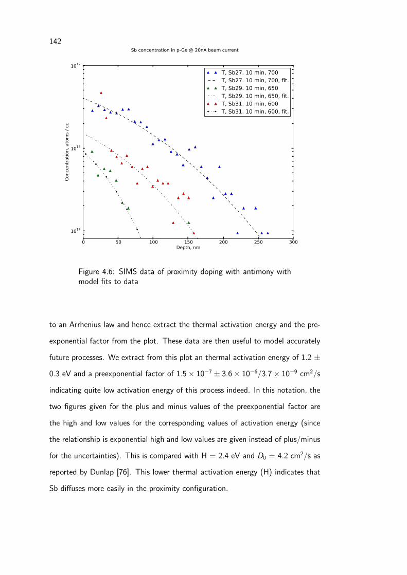
142
0 50 100 150 200 250 300Depth, nm
1017
1018
1019Conce
ntration, ato
ms
/ cc
T, Sb27. 10 min, 700T, Sb27. 10 min, 700, fit.T, Sb29. 10 min, 650T, Sb29. 10 min, 650, fit.T, Sb31. 10 min, 600T, Sb31. 10 min, 600, fit.
Sb concentration in p-Ge @ 20nA beam current
Figure 4.6: SIMS data of proximity doping with antimony withmodel fits to data
to an Arrhenius law and hence extract the thermal activation energy and the pre-
exponential factor from the plot. These data are then useful to model accurately
future processes. We extract from this plot an thermal activation energy of 1.2 ±
0.3 eV and a preexponential factor of 1.5× 10⁻⁷ ± 3.6× 10⁻⁶/3.7× 10−9 cm2/s
indicating quite low activation energy of this process indeed. In this notation, the
two figures given for the plus and minus values of the preexponential factor are
the high and low values for the corresponding values of activation energy (since
the relationship is exponential high and low values are given instead of plus/minus
for the uncertainties). This is compared with H = 2.4 eV and D0 = 4.2 cm2/s as
reported by Dunlap [76]. This lower thermal activation energy (H) indicates that
Sb diffuses more easily in the proximity configuration.

143
1.00 1.02 1.04 1.06 1.08 1.10 1.12 1.14 1.161000 / T, mK−1
10-14
10-13
10-12
Diffusivity, D, cm
2s−
1
H = 1.2 ± 0.3 eV, D0 = 1.5e-07 ± 3.6e-06 / 3.7e-09 cm2 /s
Arrhenius plot of diffusivity
Figure 4.7: Arrhenius plot of extracted diffusivities for Sb in Ge
This may be due to partial evaporation of Ge itself at elevated temperatures,
facilitating dopant in-diffusion. Another issue may be that the target wafer itself
undergoes some stress as a function of heating in the table like configuration,
where the sample is supported by support wafer fragments. This stress may also
facilitate the diffusion process, lowering the thermal activation energy. Finally, the
wafers themselves, being fairly poor quality VGF wafers, may have a high defect
density and this may have affected the diffusivity, enabling the dopant to diffuse
more readily for a given temperature.
Under the assumption that surface concentration of dopant at the surface of
the wafer in the proximity configuration should also follow Arrhenius law, we can
plot the surface concentration as a function of inverse temperature for the data.
This is depicted in Fig. 4.8.
In Fig. 4.8, we can see a reasonably linear relationship between log of

144
1.00 1.05 1.10 1.15 1.201000 / T, mK−1
1017
1018
1019
Surface
conce
ntration, N
0, cm
−3
H = 1.1 ± 0.3 eV
Arrhenius plot of surface concentration N0
Figure 4.8: Arrhenius plot of extracted surface concentrationsfor Sb in Ge
N0, the surface concentration, and 1000/T , the inverse temperature. This tends
to suggest that the surface concentration for a given time period (in this case,
10 minutes) is a thermally activated process following an Arrhenius law. This
information may be used to model the process at a later stage, by providing a
model for the surface concentration and diffusivity for proximity doped antimony
processes of comparable time and temperatures.
4.7.4 Proximity doping with GaB260 spin-on film: Gallium diffusion
In an identical manner to the previous section, Ga proximity doped Ge sam-
ples were examined using the ion-microprobe at the University of Western Sydney.
Depicted in Fig. 4.9 is the data for 4 target wafers diffused from GaB260 (the spin-
on dopant product) source wafers at temperatures from 800 to 875 C . This shows

145
that quite a large proportion of gallium was diffused, with surface concentrations
ranging from ≃ 1e19 − 1e20 cm−3 as a function of temperature. This indicates
that as in the previous case with degenerate gallium doping having been achieved
using the “sandwich-stacked” diffusion technique, for the higher temperatures,
degenerate doping can be achieved using the proximity doping technique. This
also reaffirms and supports the previous measurements for “sandwich-stacked”
diffusion.
0 200 400 600 800 1000 1200Depth, nm
1015
1016
1017
1018
1019
1020
1021
Concentration, atoms / cc
T, Ga18, 875 Deg. C, 10 minT, Ga18, 875 Deg. C, 10 min, fit.T, Ga20, 850 Deg. C, 10 minT, Ga20, 850 Deg. C, 10 min, fit.T, Ga22, 825 Deg. C, 10 minT, Ga22, 825 Deg. C, 10 min, fit.T, Ga24, 800 Deg. C, 10 minT, Ga24, 800 Deg. C, 10 min, fit.
Gallium concentration in n-Ge @ 20nA beam current
Figure 4.9: Proximity doping of Ge with gallium, showing SIMSempirical data and model fits
By comparing Fig. 4.10 and Fig. 4.3, we see a huge difference in the ther-
mal activation energy between the proximity diffused samples and the “sandwich-
stacked” diffusion samples (and published data [78, 76]). With a thermal activa-
tion energy of only 1.9 ± 0.7 eV, the diffusion has occurred much more rapidly at

146
lower temperatures than expected by the previous model. Again the explanation
may be a combination of Ge outdiffusion of the target wafer and mechanical stress
undergone in the diffusion chamber. In any case, it is handy to know that diffusion
can occur at lower energies (i.e. more rapidly for a given temperature) as this may
be of advantage for some processes.
0.86 0.87 0.88 0.89 0.90 0.91 0.92 0.93 0.941000 / T, mK−1
10-14
10-13
10-12
Diffusivity, D, cm
2s−
1
H = 1.9 ± 0.7 eV, D0 = 8.4e-05 ± 0.14 / 2.8e-06 cm2 /s
Arrhenius plot of diffusivity
Figure 4.10: Arrhenius plot of extracted diffusivities for Ga in Geusing proximity doping
The Arrhenius plot of surface concentration as a function of temperature
in Fig. 4.11 shows again a reasonably linear curve. These data may be used to
model the process in process models to determine the surface concentration and
diffusivity as a function of temperature.

147
0.86 0.87 0.88 0.89 0.90 0.91 0.92 0.93 0.941000 / T, mK−1
1019
1020
Surface concentration, N
0, cm
−3 H = 3.2 ± 0.5 eV
Arrhenius plot of surface concentration N0
Figure 4.11: Arrhenius plot of extracted surface concentrationsfor Ga in Ge using proximity doping
4.7.5 Proximity doping with phosphorus
In this experiment, proximity doping was investigated from phosphorus sources
(P507, P509 SOD films from Filmtronics, [Butler, PA, United States]). The differ-
ence between the two spin-on dopant source films is the phosphorus concentration,
4% for P507 and 15% for P509. The samples were profiled with a 50 nA SIMS
beam current as this gave the best results for most profiles. The profiles are de-
picted in Fig. 4.12. The profiles cannot be fit to a standard erfc diffusion profile
since phosphorus diffuses extrinsically in Ge [90], that is, the diffusivity is a function
of the intrinsic carrier concentration and the dopant concentration, viz. [36]:-
Di = D intri ·
1 + β−i · n
ni+ β=
i ·(
nni
)2
+ β+i · p
ni
1 + β−i + β=
i + β+i
(4.12)
where Di is the effective diffusivity, D intri is the intrinsic diffusivity β−
i is the

148
0 100 200 300 400 500 600 700Depth, nm
1017
1018
1019
1020Concentration, atoms / cc
3T. 800 Deg. C, 6 min,P50911T. 800 Deg. C, 6 min,P5075T. 750 Deg. C, 6 min,P507
P concentration in p-Ge @ 50nA beam current
Figure 4.12: Proximity doping from phosphorus spin-on dopantsource
weighting of singly negatively charged vacancies, β=i is the weighting of neutral
vacancies, and β+i is the weighting of singly positively charged vacancies.
This has the effect that the diffusivity is much higher than usual if the free
electron concentration significantly outweighs the intrinsic carrier concentration.
This tends to distort the profiles and render them fairly abrupt. The profiles are
fit using a non-linear model in Section 4.7.7.
4.7.6 Direct spin-on doping with phosphorus
Lastly, we consider directly spin-on doping the target wafer using phospho-
rus films (specifically, the P507 spin-on dopant product). This is in general to
be avoided since the dopant films themselves are inhomogeneous and prone to

149
cracking. This creates non-uniformly doped layers within the semiconductor. The
spin-on dopant films themselves may contain trace elements of contaminants that
are not advisable to bring into contact with the wafer surface. This may contam-
inate the wafer and bring about lifetime degradation. Nevertheless, direct spin-on
doping with phosphorus brings about the best looking depth profiles, with abrupt
junctions and box-like morphology.
0 200 400 600 800 1000 1200 1400Depth, nm
1016
1017
1018
1019
1020
1021
1022
1023
Concentration, atoms / cc
SOD matrix
Ge matrix
4S. 750 Deg. C, 6 min,P5076S. 700 Deg. C, 6 min,P5078S. 655 Deg. C, 6 min,P507
P concentration in p-Ge @ 50nA beam current
Figure 4.13: Direct spin-on doping with phosphorus spin-ondopants.
In Fig. 4.13 we see an initial ≃ 340nm region which is the spin-on dopant
matrix itself. Thereupon the ion microprobe cuts its way through the SOD matrix
into the underlying Ge wafer (Ge matrix). This is due to the fact that the source
wafers did not have the spin-on dopant films removed prior to SIMS analysis, so
that the makeup of the SOD matrix itself could be studied. In all 3 cases, the SOD

150
Sample Temperature (C ) Time (s) Approx. junction depth (nm)
4S 750 360 923
6S 700 360 593
8S 650 360 333
Table 4.11: Approximate junction depth of spin-on doped sam-ples
matrix appears to have the same shape, and hence the phosphorus concentration
is consistent sample to sample. However obtaining accurate results from the ion
microprobe with insulating coatings is difficult, so not much can be quantatively
assessed from these data. This is due to charging affects which interfere with the
ion beam and distort results.
The abrupt profiles are due, once again, to extrinsic diffusion, the mechanism
by which the diffusivity becomes proportional to the quotient of the free electron
concentration and the intrinsic carrier concentration. The approximate junction
depths for the three samples investigated in Fig. 4.13 are tabulated in table Tab.
4.11.
4.7.7 Fit to phosphorus depth profiles using non-linear model
In order to extract the diffusivity of phosphorus, the diffusion equation (Fick’s
second law, Eqn. 4.6) must be solved numerically with a non-linear model for the
diffusivity at each mesh point, viz.:-
Dext ≃ D
(
Cphos
ni
)2
(4.13)
since we assume that the term involving neutral vacancies of Eqn. 4.12
dominates. Profiles are first normalised to remove any initial portions of the SIMS

151
data that contain sputtering of surface materials such as SOD films or surface
coatings from the diffusion process. In the case of the direct spin-on samples, the
concentration is clipped at the solubility limit of the material at that temperature
as determined from the SIMS data itself. This produces a ”squaring-off” of the
profiles in the fitted data.
0 200 400 600 800 1000 1200 1400Depth, nm
1017
1018
1019
1020
Concentration, atoms / cc
Fits to depth profiles using non-linear model
8S. 655 Deg. C, 6 min,P507Model fit6S. 700 Deg. C, 6 min,P507Model fit4S. 750 Deg. C, 6 min,P507Model fit5T. 750 Deg. C, 6 min,P507Model fit3T. 800 Deg. C, 6 min,P509Model fit11T. 800 Deg. C, 6 min,P507Model fit
Figure 4.14: Fit to depth profiles using non-linear model
It is difficult to fit to the data from samples which are directly spun-on. This
is most likely due to the extremely high surface concentration of dopant above
the solid solubility limit of the film [22]. This has an effect on the surface of the

152
sample, warping the crystal lattice and introducing higher-order effects not taken
into account by this simple model. Nevertheless, the model fits are of reasonable
accuracy. The model fits to data for both phosphorus “proximity”- and direct
spin-on doping are shown in Fig. 4.14.
0.90 0.95 1.00 1.05 1.10 1.151000 / T, mK−1
10-15
10-14
10-13
10-12
10-11
Diffusivity, D, cm
2s−
1
H = 3.1 ± 1.1 eV, D0 = 1.3e+03 ± 0.3 / 3.9e+08 cm2 /s
Arrhenius plot of phosphorus diffusivity
Figure 4.15: Arrhenius plot of phosphorus diffusion in Ge
An Arrhenius plot of extracted diffusivities is shown in Fig. 4.15. The
extracted activation energy is 3.1 ± 1.1 eV, which is higher than reported in the
literature, 2.4 eV [76]. This may be due to difficulties in fitting the data and the
inaccuracy of the fits, but in all likelihood this is a reasonable figure, particularly
when extracted under extrinsic conditions (the data of W.C Dunlap Jr. [76] is
for the case of intrinsic diffusion). Nevertheless the published data is within this
uncertainty range, which is quite large due to conflicting measurements at the
same temperature.

153
4.8 Conclusions
A novel technique, “sandwich-stacked diffusion”, for the degenerate doping
of Ge, has been presented. The thermal activation energies and pre-exponential
factors have been extracted for both diffusion into low doped p-type and n-type Ge
wafers, and are found to be in agreement with published data, within experimental
error. While thorough conclusions could not be drawn about the nature of the Ga
diffusion process in this work, this technique provides a simple, low cost, method
to further investigate diffusion of acceptors in Ge, which for practical reasons can
be problematic.
An approximate analytical model has been derived to describe the doping
profile, which may be used to design and fabricate devices. Processes may be
tuned by simple sheet resistance measurements in conjunction with this analytical
model.
This technique is suitable for low-cost processing of Ge devices for a wide
range of applications, including degenerate doping for tunnel FETs and Esaki
diodes for high frequency and low power devices, and degenerate doping for back
surface fields in photovoltaic and thermophotovoltaic devices.
In this section we have also presented data for “proximity” diffusion and
direct spin-on doping using phosphorus. We have compared “sandwich-stacked
diffusion”, the novel technique developed in this work, with “proximity doping”
and direct spin-on doping. Direct spin-on doping should be avoided due to peeling
and cracking of the film due to CTE (coefficient of thermal expansion) mismatch
between the silica films and the germanium wafers, and inhomogeneities and con-
taminants in the spin-on dopant films. Nevertheless, we saw that direct spin-on
doping had a more abrupt and hence advantageous profile as compared to proxim-
ity doping for phosphorus spin-on dopant sources. This could be useful for creating

154
tunnel diodes and other such devices.
It was shown that degenerate p-type doping is possible both with sandwich
stacked diffusion as well as with proximity doping with gallium. However the
thermal activation energy was seen to be much lower for the proximity doping
case. This was attributed to a combination of mechanical stress on the wafer
during the process as well as Ge out-diffusion and partial evaporation.
Some concerns may be raised about the discrepancy in results recorded for
Ga diffusion by the two techniques. Firstly, different equipment was used to char-
acterise the two sets of samples. Since SIMS profiling is destructive, it is difficult
to profile the same sample on both sets of equipment to ensure that discrepancies
are not due to equipment related error. Hence such comparisons were not per-
formed. However, since depth is measured on the resultant craters using a stylus
profilometer, in spite of differences in sputtering rate on the two pieces of equip-
ment, the depth profile data should be accurate. The ion yield was calibrated on
the UWS equipment by means of ion implanted samples so should be more trust-
worthy than the data from the National University of Singapore, which had to be
calibrated using sheet resistances. The two sets of equipment were employed in
this study purely for reasons of cost; it was less expensive to profile a large number
of samples at the University of Western Sydney. However, the equipment at UWS
was in poorer condition than that of the National University of Singapore. This
resulted in noisy data for low ion yield samples such as the antimony samples.
Nevetheless it is concluded that the discrepancy in data obtained for Ga diffusion
is purely a function of the above mentioned effects and not equipment related.
Since the techniques described herein were applicable to rapid thermal pro-
cessing, we anticipate that they would be readily amenable to mass manufacture
and hence low cost in a manufacturing environment, as is necessary for devices in
the solar cell manufacturing sector.
Chapter 5
Passivation, antireflection, and contacting technologies for germanium
optelectronic devices
5.1 Introduction
In this chapter we present the critical passivation, antireflection and con-
tacting technologies developed for this work. Device passivation has three main
purposes: to terminate the sensitive semiconductor lattice and passivate any dan-
gling bonds at the surface which may impair device performance, to protect sen-
sitive device regions such as junctions from impurities and inclusions which may
cause catastrophic device failure, and to protect the device from moisture and
atmospheric impurities during subsequent device processing or storage. Antireflec-
tion coatings are used to account for the mismatch in refractive index between
germanium and any material onto which it may interface along the optical path
to the photon source; an example would be the mismatch between the refractive
index of air and the semiconductor itself. Our simple passivation/antireflection
coating technology is shown to reduce reflection losses of a single junction germa-
nium solar cell under AM1.5G illumination to under 10%, which is adequate, since
surface texturing can be used to further reduce reflection losses (assuming light
trapping texturing). A reflectivity of 10% is a fair trade-off between an optimal
structure and a practical structure in terms of cost and complexity. For instance,
the emphasis in this work is on practical materials that are readily available to solar

156
cell processes and which are low in cost, which is a higher priority than absolutely
optimal optical matching using more exotic materials.
Contact metallisation is discussed in this section and a variety of contact
metals are evaluated. The purpose is to engineer low resistivity contacts to ger-
manium to lower losses due to series resistance.
5.2 Passivation of germanium
Germanium electronic and optoelectronic devices have historically suffered
due to lack of a stable native oxide as passivation layer [91, 92]. In this work, we
are careful to distinguish between the many different processes which are generally
lumped together under the umbrella of passivation - that is, wet chemical treat-
ment/dry chemical pretreatment (i.e. pretreatment for dangling bond termination
and to prevent oxidation of the surface), passivation layers (e.g an insulator or
wide band gap semiconducting overlayer to prevent surface leakage currents, and
act as a template for deposition of further layers) and finally environmental passi-
vation (to prevent issues such as moisture/contaminant ingress). It must be noted
however, that effective passivation methods for formation of high quality interfaces
for gate stack formation (e.g. for high frequency CMOS applications) are not con-
sidered in this work, which is intended solely to address the need for stable, high
quality passivation/anti-reflection (AR) coating for optoelectronic applications.
With respect to the first of the three above passivation processes, i.e. chem-
ical pretreatments, the following have been shown to be effective in terminating
dangling bonds at the Ge surface: hydrogenation [26, 93, 94, 95], passivation
with halides HCl or HCl/HBr [79, 96, 97, 98], sulphidation with H2S [99] or
(NH4)2S [80, 100, 101], and nitridation with in-situ NH3 or N2 (or both) as gas
(at high temperature) or plasma (at lower temperatures) [102, 103, 104, 105].
Hydrogenation can be performed using wet treatments of HF and DI water and

157
using in-situ H2 plasma [26]. There is also evidence of organic compounds pas-
sivating the germanium surface, yielding low surface recombination velocities (∼
20 cm/s) [106].
Regarding passivation layers, germanium has been capped with phosphorosil-
icate glass (PSG) [107], III-V materials such as InGaAs/GaAs [56], a-Si:H [26],
chemical vapour deposited (CVD) SiNx, Ge3N4 [105] and high-κ dielectrics such
as TaN, HfO2, sometimes in combination with thermally grown GeO2 [105]. MgO
has also been investigated [101], in combination with sulphur wet treatment, to
de-pin the Fermi level at the surface of the Ge. A CVD-deposited silicon interlayer
between Ge and the passivation layer has shown to reduce interface traps and yield
good MOS characteristics [108].
These technologies however have their drawbacks, in terms of processing
temperature for passivation layer deposition (i.e. 600C for SiNx deposition, or
oxide growth [105]), which would destroy device junctions (due to diffusion), or in
terms of the fact that they cannot be heated to high temperatures post passivation
(as in a diffusion/drive-in/implant activation step, or subsequent high temperature
treatment) without damage to the passivation layer. In this section, we compare
published passivation technologies for optoelectronic devices and present a novel
low temperature, low cost inductively-coupled plasma enhanced chemical vapour
deposition (ICPECVD) based passivation technology which shows excellent perfor-
mance for use in optoelectronic devices. We review surface wet/dry pre-treatment
methods and demonstrate the importance of adequate surface pre-treatment to
well passivated devices. The anti-reflection properties of the passivation layer stack
are considered, and we show that it is possible to optimise both, giving a three
layer anti-reflection coating (ARC) consisting of a-Si:H/SiNx/MgF2 which shows
excellent chemical and environmental robustness, low reflectance, high transmis-
sion and low surface recombination velocity (SRV).

158
5.2.1 Experimental
5.2.1.1 Sample preparation
Photoconductors were prepared for photoconductive decay measurements
from low doped (∼40 Ohm·cm) n-type Ge<211> wafers [Umicore, Olen, Belgium]
by cleaning (soak in warm trichloroethylene, acetone, methanol plus ultrasonic
bath), pre-treatment and passivation layer deposition, and finally depositing Cr/Au
Schottky contacts after stripping the passivation layer using reactive ion etching
(RIE) from the contact pad regions.
It has been noted that surface pre-treatment prior to passivation is important
to reducing SRVs and reducing interface trap densities. Two main wet treatments
are investigated in this work: HF/H2O, and HCl/HBr. HF/H2O treatment has
been shown to strip native oxides and terminate the Ge surface with hydrogen
[109]. HCl/HBr has been shown to passivate dangling bonds and leave the surface
terminated with Cl [110] or potentially Br. This treatment is carried out at room
temperature, since at elevated temperatures, this solution can etch the germanium
surface and potentially consume device active regions. Each treatment is preceded
with a 30s dip in 1:1:5 NH4OH : H2O2 : DI to remove approx 100nm of the surface
damaged region of the wafer (i.e. due to sawing) and any diffused impurities at
the surface. The chemical treatments are tabulated in Tab. 5.1.
5.2.1.2 Dry pre-treatment
Two main plasma treatments are considered in this work, namely H2, and
NH3 plasmas. The purpose of the dry plasma treatment is much the same as the
wet treatment, i.e. to desorb any native oxides and passivate dangling bonds. It
has been suggested that ammonia plasma treatment leaves the surface terminated
with nitrogen [4]. Whilst the ammonia pre-treatment can be carried out in-situ

159
Treatment Steps
A - Hydrogenation
1. Dip 1:1:5 NH4OH:H2O2:DI 30s
2. HF dip (1:3 BOE), 1 min
3. DI soak, 3 min
B - Halide Passivation1. Dip 1:1:5 NH4OH:H2O2:DI 30s
2. 1:1:5 HCl:HBr:DI soak, 1 min
Table 5.1: Wet pre-treatments for Germanium passivation
Treatment Gas flow rate Plasma Power
A. H2 plasma (ex situ) 10 sccm RF, 15W 30s
B. NH3 plasma (in situ) 10 sccm ICP, 200W 30s
Table 5.2: Dry pre-treatments for Germanium passivation
within the ICPEVCD reactor, the hydrogen plasma treatment was performed in a
separate tool, a Plasmalab System 100 RIE from Oxford Instruments [Austin, TX,
USA]. It must be noted that the brief exposure to atmosphere when transferring
to the ICPECVD after H2 plasma treatment may negate some of its beneficial
effects. The basic recipes are described in Tab. 5.2. The ammonia treatment
took place at 250 C , whereas the H2 plasma treatment was performed at room
temperature.
5.2.1.3 Passivation layer deposition
In this work we consider SiNx, a-Si:H/SiNx, and SiO2 as potential passivation
layers. These are deposited in a Sentech SI500D ICPECVD [Sentech Instruments
GmbH, Berlin, Germany]. The recipes are shown in Tab. 5.3. It was noted in
previous experiments that low ICP power favours higher quality SiO2 and a-Si:H

160
MaterialTable
temp. ( C)Flow rates ICP Power
SiO2 120 SiH4 = 6.5 sccm 450W
He = 123 sccm
Ar = 126 sccm
O = 70 sccm
a-Si:H 300 SiH4 = 5 sccm 35W
Ar = 95 sccm
SiNx 100 SiH4 = 7.3 sccm 800W
Ar = 139 sccm
NH3 = 10 sccm
Table 5.3: Passivation layer film deposition parameters
with good optical and mechanical properties and resilience to high temperature
processing, however for SiNx, the reverse is true. Here SiNx is deposited at very
high (∼ 800 W) ICP power, which furnishes very high quality, chemically resistant
SiNx with wide area uniformity (> 5” diameter uniformity area).
5.2.1.4 Anti-reflection coatings
In order to investigate the potential for combining a-Si:H, SiNx and MgF2
as both passivation and anti-reflection (AR) coating, films were first deposited
individually on germanium in order to obtain optical constants using spectroscopic
ellipsometry. This data was then used to optimise AR film parameters. Whereas
a-Si:H and SiNx were deposited in the Sentech ICPECVD, MgF2 was evaporated
in a bell-jar thermal evaporator at a rate of 0.5-1 A/S. Optical constants (complex
refractive index) and thicknesses were extracted by spectroscopic ellipsometry using
a Woollam M2000D [J. A. Woollam Co., Lincoln, NE, USA].

161
5.2.1.5 Contact deposition
Contacts were deposited using thermal evaporation of 5nm Cr and 50nm Au
at a rate of 0.5 A/s (Cr) and 10 A/s (Au), respectively, in a bell jar evaporator
at a vacuum of 1e-6 Torr. The contacts were patterned using photo-lithography
and lift-off patterning, and lift-off was performed in boiling acetone, with residual
resist removed using a swab dipped in hot acetone.
5.2.2 Characterisation
5.2.2.1 Photoconductive decay
PMOS
White LED
Sample under test
To power supply
To square
wave generator
probes
To parameter
analyser
To parameter
analyser
Test structure viewed from above
Contact
pads
Mesa
Bulk
+ -Applied bias
Figure 5.1: Measurement setup for photoconductive decay mea-surements
Photoconductive decay measurements were undertaken by illuminating the
device with a white LED broadband source pulsed at 100 Hz. The test setup is
shown in Fig. 5.1, which also shows a photoconductor viewed from above. The

162
mesa region of the photoconductors was 40 µm wide and between 96 and 900
µm long. Devices were biased at 30V, in order to ensure significant photocurrent.
The white LED was switched using a p-channel MOSFET with switching times
several orders of magnitude shorter than the minority carrier lifetime. Since the
surface recombination velocity (SRV) is essentially a boundary condition on the
drift diffusion equations (i.e. for holes dp
dx|surface = S ·p where S is the SRV, p is the
hole concentration) a useful expression can be derived by solution of the diffusion
equation [111]. If we make the assumption that S is much less than the diffusivity
of electrons divided by half the wafer thickness (= 500 µm ), in this case roughly
4000 cm/s, then we can make use of the following expression relating the effective
lifetime to the bulk lifetime and S [26]:
1
τeff=
1
τbulk+
1
τSRV=
1
τbulk+
2S
d(5.1)
where τeff is the effective lifetime, τSRV is the surface recombination dom-
inated lifetime, τbulk is the bulk lifetime, S is the surface recombination velocity
(total for both sides) and d is the wafer thickness. The effective lifetime is taken
to be the dominant decay curve of a potentially multi-exponential curve [112].
The bulk lifetime was assumed to be roughly 3.8 ms, a value taken from
the literature [26]. In [26] this value was determined for wafers of comparable
quality from the same manufacturer as were used in these experiments so should
be approximately valid. The usual method for determining the bulk lifetime and
surface recombination velocity is to perform measurements on samples of varying
thickness. A plot of 1/τeff vs. 1/d is then constructed; the y intercept is equal to
1/τbulk and the slope is equal to 2S [26, 112]. Due to budget and time constraints,
wafers of only a single thickness were used in these experiments, hence a value for
the bulk lifetime is assumed, rather than experimentally determined.

163
EntryWet
treatment
Dry
treatmentPassivation Layer τSRV S (cm/s)
1 A A 40nm SiO2 150 µs 173
2 A A40nm a-Si:H
75nm SiNx171 µs 150
3 A A 75nm SiNx 60 µs 423
4 B B 40nm SiO2 150 µs 173
5 B B40nm a-Si:H
75nm SiNx1.7 ms 21
6 B B 75nm SiNx 60 µs 423
7 B -40nm a-Si:H
75nm SiNx78 µs 327
8 B - 75nm SiNx 40 µs 631
9 B - Unpassivated 200 µs 131
Table 5.4: Passivation layer film deposition parameters, showingwet pretreatment (see table Tab. 5.1) and dry pretreatment(see table Tab. 5.2), measured lifetime and extracted surfacerecombination velocity.
The photoconductive decay results are shown in table Tab. 5.4.
From the photoconductive decay measurements, we may draw a few infer-
ences about the various passivation processes. Firstly, the HCl/HBr pretreatment,
which has been shown previously to reduce interface state density can successfully
terminate the lattice so as to reduce surface recombination velocity, which is evi-
denced by entry 9 in table Tab. 5.4. Secondly, in situ dry treatment is preferable
to ex situ or wet treatment alone, which may be attributed to native oxide re-
moval. Finally, insulating wide band gap (optical band gap ≃ 2.2eV) amorphous
silicon is a superior passivation layer in combination with SiNx, reducing interfacial
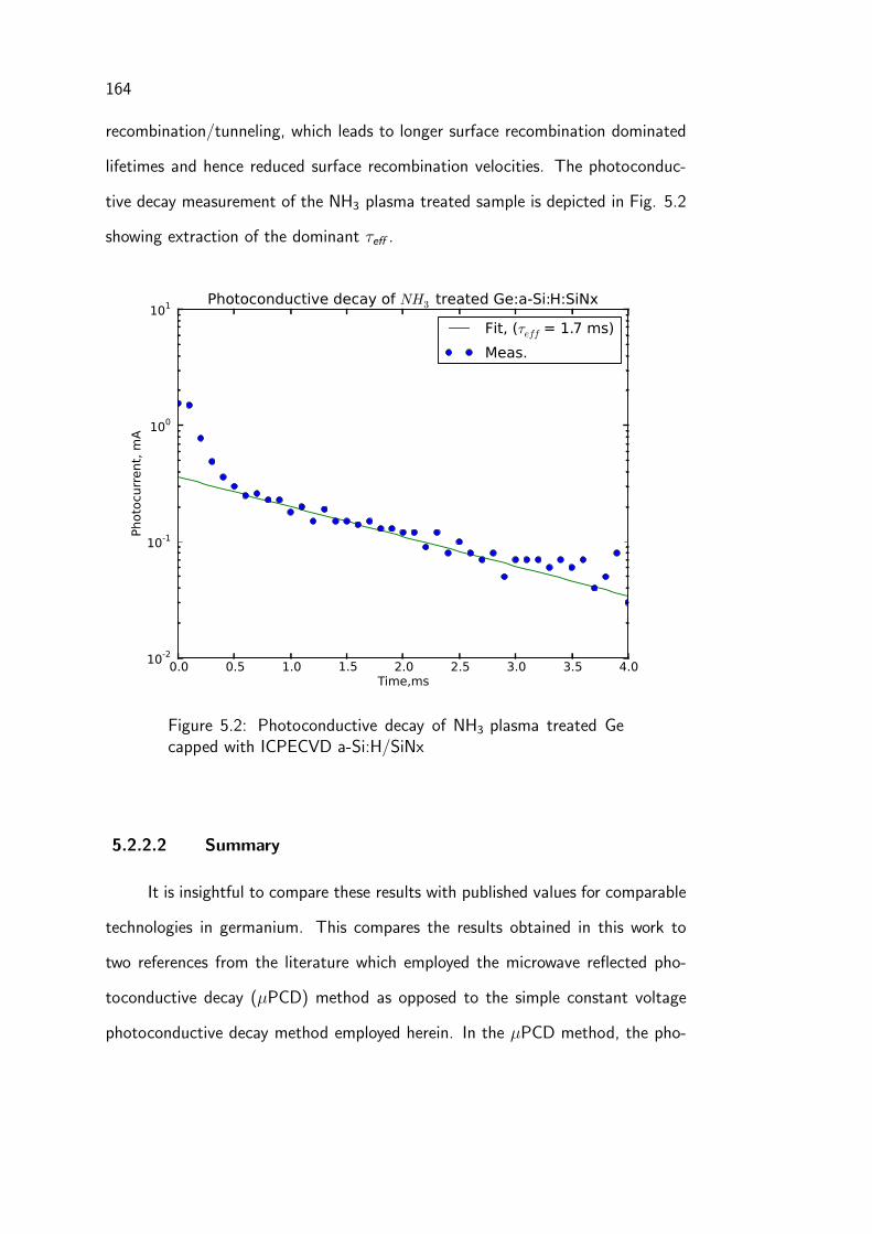
164
recombination/tunneling, which leads to longer surface recombination dominated
lifetimes and hence reduced surface recombination velocities. The photoconduc-
tive decay measurement of the NH3 plasma treated sample is depicted in Fig. 5.2
showing extraction of the dominant τeff .
0.0 0.5 1.0 1.5 2.0 2.5 3.0 3.5 4.0Time,ms
10-2
10-1
100
101
Photocurrent, m
A
Photoconductive decay of NH3 treated Ge:a-Si:H:SiNx
Fit, (τeff = 1.7 ms)
Meas.
Figure 5.2: Photoconductive decay of NH3 plasma treated Gecapped with ICPECVD a-Si:H/SiNx
5.2.2.2 Summary
It is insightful to compare these results with published values for comparable
technologies in germanium. This compares the results obtained in this work to
two references from the literature which employed the microwave reflected pho-
toconductive decay (µPCD) method as opposed to the simple constant voltage
photoconductive decay method employed herein. In the µPCD method, the pho-

165
toconductivity is measured by microwave reflection after carriers are injected by
optical pulses from a pulsed laser [85].
These results are set out in Tab. 5.5. Note that the results of Posthuma et
al. [26], while impressive, are derived from extrapolation from curves of 1/τ vs.
1/d, which gives very optimistic values for the surface recombination velocity and
bulk lifetime. Indeed the bulk lifetime seems quite high, even for very pure CZ
germanium, which tend to contradict lifetime studies as published in the literature
[113, 114], which indicate a maximum lifetime of ∼ 2ms for the bulk lifetime.
Nevertheless, this might be attributable to advances in Ge material processing,
since the first measurements of lifetime were made many decades ago. On the
other hand, the results of Swain et al. [115] seem a great deal more realistic
and serve to highlight the affinity the germanium surface has for both hydrogen
and chlorine. However, we must concede that wet treatment alone is simply not
enough to adequately passivate germanium, as it does not deal with the issues
of necessary A/R coatings nor environmental passivation. Hence, we can surmise
that wet treatment (with its reasonable stability in air) can be used to prevent
oxidation of the sample prior to loading into an ICPECVD tool to deposit capping
and A/R layers. Finally, we must point out that since the PCD technique as used in
this work involves making contacts, and that contacts are recombination centers,
the PCD results will always give shorter lifetimes than the µPCD technique, which
is a contactless microwave-reflected photoconducive decay method. Nevertheless,
we can conclude that the SRVs presented in this thesis are comparable to those
reported in the literature.
5.2.3 Anti-reflection coatings
In addition to passivation (which lowers surface recombination velocities,
thus improving photocurrent in optoelectronic devices), anti-reflection coatings are

166
Ref.Passivation
Layer stackMaterial
τeff
τbulkS (cm/s)
Meas.
techn.
Posthuma
et al. [26]
a-Si:H
∼ 100nm
p-type
CZ Ge
550µs
3.8ms17 µPCD
Swain
et al. [115]
Wet treatment
(HF
HCl)
p-type
CZ Ge
∼ 475, 370µs
1.17ms23, 37 µPCD
This
work
a-Si:H
∼ 40nm :
SiNx
100nm
n-type
CZ Ge
1.7ms
3.8ms21 PCD
Table 5.5: Summary of Germanium passivation technologies
necessary to further maximize photoresponse or efficiency of power transfer. In
this work, we consider the use of a-Si:H/SiNx/MgF2 as combined passivation/anti-
reflection (A/R) coating. This is depicted in Fig. 5.3.
Figure 5.3: Schematic diagram of proposed 3 layer A/R coating.Ei is the incident wave, Er the reflected wave. dj is the layerthickness; ηj is the refractive index of each layer.
It is informative to calculate what the optimal refractive indices ought to be
in order to totally cancel any reflections at the interfaces between layers, in order

167
to compare them with the chosen materials’ properties. In this case, we must
satisfy [33, 34]:-
η1η0
=η2η1
=η3η2
=ηSη3
(5.2)
with dj set to a quarter wavelength. A possible solution is to have η3 : η2 : η1
= 2.8 : 2 : 1.4, which is a reasonable match for a-Si:H (n ∼ 3.5) : SiNx (n ∼ 2)
: MgF2 (n ∼ 1.4).
In order to optimise this AR structure, the optical constants were first ex-
tracted for each material used in the coating. In the case of SiNx, it is known
that the refractive index can be tuned by adjusting the ammonia flow rate. For
the SiNx recipe in Tab. 5.3, refractive index as a function ammonia flow rate is
depicted in Fig. 5.4.
Figure 5.4: Refractive index (@ 632nm) vs. ammonia flow rate
Since the higher refractive index is required, the lowest ammonia flow rate
(10 SCCM) is used; lower flow rates were not considered since it was assumed
that this would disturb the governing reactions adversely and give rise to poor
quality films. Another property that is necessary to tailor is the hydrogen content
of the SiNx film; high hydrogen content will cause absorption throughout the

168
visible and infrared regions such that any anti-reflection properties would be more
than negated. High ICP power and low growth rate were seen to ensure low
hydrogen content and hence low absorption, as evidenced by the imaginary part
of the complex refractive index (i.e. k) being less than 10−5 for all wavelengths
longer than 400 nm.
This is in contrast to a-Si:H, which is deposited with low ICP power and
higher substrate temperatures to ensure high quality films. Under these limit-
ing conditions, the deposition technology approaches chemical vapour deposition
proper. These low hydrogen content films are quite robust and well suited to high
temperature processing, surviving 10-15 minute treatment at 750C without any
change in optical thickness, and without evidence of bubbling (which can occur if
H content is substantial). Optical constants of all 3 films are shown in Fig. 5.5.
Using the optical constants, 3 layer anti-reflection coatings may be designed
and optimised for a particular wavelength or spectrum. In this work, we consider
optimisation of the AR coatings for the solar (AM1.5G) spectrum for use in pho-
tovoltaic applications. The AM1.5G spectrum was chosen in order to improve the
efficiency of stand-alone Ge solar cells, as presented in chapter 6. In this work,
we do not choose to optimise for longer wavelengths, such as for the irradiation
expected in a four terminal tandem cell configuration with CdTe top cell. This is
because we the precise thickness of the CdTe top cell was not firmly determined at
time of writing. However, an identical procedure can be followed to optimise the
structure for longer wavelengths. As we shall see, the below structure shows rea-
sonable response at longer wavelengths so we wouldn’t expect much would change
if we were to optimise for the infra-red portion of the spectrum. Note that no anti-
reflection coating is required for germanium in the case of a monolithic tandem
cell; instead, we would like a reflective back contact to reflect any light reaching
the back surface back through the device. Nonetheless, adequate passivation of

169
0 500 1000 1500 2000
Wavelength (nm)
0
0.5
1
1.5
2
2.5
3
3.5
4
4.5R
efr
acti
ve index, n
SiNx a-Si:H MgF2
Optical properties of films
Figure 5.5: Refractive indices of films used for passivation/ARcoating
the back surface is crucial to reducing back surface recombination velocities so
the structure presented below is still applicable to a monolithic tandem to improve
electronic properties of the back surface.
The optical stack is optimised by evaluating the usual expressions for the
reflectance (R), transmittance (T) and absorption (A) of the multilayer film [33,
34]:
R =
(
η0B − C
η0B + C
)(
η0B − C
η0B + C
)∗(5.3)
T =4η0Re(ηS)
(η0B + C )(η0B + C )∗(5.4)
A = 1− R − T =4η0Re(BC
∗ − ηS)
(η0B + C )(η0B + C )∗(5.5)
170
where:
B
C
= Meq
1
ηS
(5.6)
Meq =n∏
j=1
cos(φj)iηjsin(φj)
iηj sin(φj) cos(φj)
(5.7)
η0 = Y0 = ǫ0 · c0 (5.8)
ηS = Y0(nS − ikS) (5.9)
ηj = Y0(nj − ikj) (5.10)
(5.11)
φj =2πηj · dj
λ(5.12)
where Y0 is the permittivity of free space and nl , kl are the refractive index
and extinction coefficient of medium l respectively (l = 0 = air, l = S = substrate,
l = j = layer j, etc.) and λ is the wavelength.
Although dispersion in the films is comparably small, it cannot be neglected
entirely, necessitating solution for the optimal structure via numerical (i.e. global
solution), rather than analytical means (i.e. for one particular wavelength). This
allows one to generate a 3 dimensional dataset to optimize the optical properties
of the film stack, as weighted over the AM1.5G spectrum, in order to maximize
energy transfer to the underlying device.
Fig. 5.7 shows the slice through the data cube for d1 = 90 nm, showing
reflection, transmission, and absorption characteristics as a function of the two
remaining free parameters, d2 and d3.
The amorphous silicon films are highly absorptive. This is due in part to the
above band gap absorption of the films (the optical bandgap of the amorphous
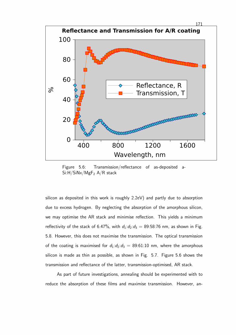
171
400 800 1200 1600
Wavelength, nm
0
20
40
60
80
100
%
Reflectance, RTransmission, T
Reflectance and Transmission for A/R coating
Figure 5.6: Transmission/reflectance of as-deposited a-Si:H/SiNx/MgF2 A/R stack
silicon as deposited in this work is roughly 2.2eV) and partly due to absorption
due to excess hydrogen. By neglecting the absorption of the amorphous silicon,
we may optimise the AR stack and minimise reflection. This yields a minimum
reflectivity of the stack of 6.47%, with d1:d2:d3 = 89:58:76 nm, as shown in Fig.
5.8. However, this does not maximise the transmission. The optical transmission
of the coating is maximised for d1:d2:d3 = 89:61:10 nm, where the amorphous
silicon is made as thin as possible, as shown in Fig. 5.7. Figure 5.6 shows the
transmission and reflectance of the latter, transmission-optimised, AR stack.
As part of future investigations, annealing should be experimented with to
reduce the absorption of these films and maximise transmission. However, an-

172
75 80 85 90 95 100 105 110 MgF2 thickness, nm
79.20
79.25
79.30
79.35
79.40
79.45
79.50
79.55
79.60
Tra
nsm
issi
on,
%
T = 79.57 % MgF2 = 90 nm SiNx = 61 nm a-Si:H = 10 nm
Transmission vs. MgF2 thickness
0.02 0.04 0.06 0.08 0.10 SiNx thickness, m
0.02
0.04
0.06
0.08
0.10
a-S
i:H t
hic
kness
,
m
45.0%
55.0%
65.0%
75.0%
Transmission vs. layer thickness MgF2 = 90 nm
0.02 0.04 0.06 0.08 0.10 SiNx thickness, m
0.02
0.04
0.06
0.08
0.10
a-S
i:H t
hic
kness
,
m
8.0%
8.0%
10.0%
10.0%
12.0%
14.0
%
14.0%
16.0%
16.0
%
18.0%
Relectivity
0.02 0.04 0.06 0.08 0.10 SiNx thickness, m
0.02
0.04
0.06
0.08
0.10
a-S
i:H t
hic
kness
,
m
16.0%
26.0%
36.0%
Absorption
Figure 5.7: Optimisation of as-deposited a-Si:H/SiNx/MgF2 A/R stack
75 80 85 90 95 100 105 110 MgF2 thickness, nm
6.4
6.5
6.6
6.7
6.8
6.9
7.0
7.1
Reflect
ivit
y,
%
R = 6.47 % MgF2 = 89 nm SiNx = 58 nm a-Si:H = 76 nm
Reflectivity vs. MgF2 thickness
0.02 0.04 0.06 0.08 0.10 SiNx thickness, m
0.02
0.04
0.06
0.08
0.10
a-S
i:H t
hic
kness
,
m
8.0%
8.0%
10.0%
10.0%12.0%
14.0
%
14.0%
16.0%
16.0
%
18.0%
Reflectivity vs. layer thickness MgF2 = 89 nm
Figure 5.8: As-deposited a-Si:H/SiNx/MgF2 A/R stack: optimalreflectivity
173
nealing will cause the silicon to recrystallise, narrowing the optical band gap and
altering optical characteristics. Such final optimisations are beyond the scope of
this work.
5.3 Contacts to Germanium
A number of contact metals have been considered for germanium since the
inception of germanium semiconductor research and device processing. For exam-
ple, the traditional method of contacting to n-Ge used antimony (≃ 1%) doped
gold, with the antimony acting as a dopant to heavily dope the region beneath
the contact, lowering contact resistance and improving Ohmicity.
One difficulty with making reliable, Ohmic or Schottky contacts to germa-
nium is Fermi-level pinning [116, 117, 80]. Interface states pin the Fermi level
at the Ge surface, typically resulting in Schottky behaviour on n-type material or
at the very least poor contact resistivity, and always ohmic behaviour on p-type
material [117]. This has a major impact on the quality of contacts that can reliably
be formed.
More recently, Ni has been investigated [116] as a contact to heavily doped
n-Ge. This process involved annealing the contacts to form an interlayer of NiGe
at temperatures of 340 C. It was thought that this interlayer allowed better
tunnelling through the Schottky barrier at the Ge/Ni interface [116]. Lieten et
al. [117] investigated a number of contact materials to Ge in conjunction with
an interlayer of Ge3N4 to mitigate Fermi-level pinning at the Ge surface. Metals
investigated include Al, Cr, Co, Au, and Pt. Thathachary et al. [80] reported on
the use of aqueous ammonium sulphide ([NH4]2S) treatment to perform Fermi-
level depinning for metallic contacts featuring Al, Zr, Ta, W, Ni and Pt.
174
5.3.1 Derivation of specific contact resistivity for some contact met-
als
In this work, we investigated a range of contact metals available in the UWA
clean room including Au, Pt, Al, In, Ni and Ti to heavily n-type doped material.
Indium (In) did not form a very reliable contact to Ge so no data could be
collated. The material itself formed a non-uniform film on the Ge surface which
scratched when the device was probed and displayed rectifying properties. Similar
difficulties arose when trying to use Pt as the contact material. Pt itself should
be reasonably compatible with the Ge surface, however it may have required an
interlayer for adhesion, for example Ti or Cr, in order to bond to the Ge surface
adequately.
5.3.1.1 Mask for contact resistivity measurements and diode fabri-
cation
The mask design for contact resistivity measurements and diode fabrication is
shown in Fig. 5.9. It features a number of test structures such as linear and circular
transfer length method structures, Kelvin resistance structures, diodes, JFETs,
hall bars, and fixed resistances. These test structures were designed to enable
characterisation on a single die of a wide variety of parameters for a particular
process. These include hall mobility, diode IV characteristics, resistance, specific
contact resistivity, sheet resistance, etc. Hence this particular mask set is well
suited to process characterisation.
5.3.1.2 Transfer length method
The linear transfer length method is a simple technique for determining
the specific contact resistivity and sheet resistance of a specially designed contact

175Circular TLM Structures
Linear Transmission Lines
Fixed value resistanceDiode structures
Hall bars
Kelvin resistance structures
JFETs
Figure 5.9: Mask set design
structure. This structure is a linear strip of contacts separated by unequal distances
d1, d2 ... dn but w wide and L long. The structure is detailed in Fig. 5.10.
L
w
Figure 5.10: Transmission line construction

176
Contact separation, d (cm)
Figure 5.11: Transmission line graph
The resistance between each successive rung on the ladder is measured and
plotted against the distance between contacts (see Fig. 5.11 for an example of the
plot). Three pieces of information can be deduced from this plot [85]. The sheet
resistance is given by the slope of the plot, with RSH = slope× w. The intercept at
d=0 gives the contact resistance; at d = 0, RT = 2RC [85]. The transfer length is
then given by the intercept at RT = 0, −d = 2LT, from which the specific contact
resistivity ρc can be computed using the following [85]:-
LT =√
ρc/RSH (5.13)
5.3.1.3 Circular Transfer Length Method
The above linear transmission line method is readily adapted to circular
structures where it can be more easily processed and corrected for (since there are
no current crowding effects in circular structures that occur at the edges of the
linear structures, since no mesa is required as the structures are self-isolating [116]).
The circular structures are created as follows. A disc of radius r is surrounded by
an annulus separated by gap spacing d , as shown in Fig. 5.12.
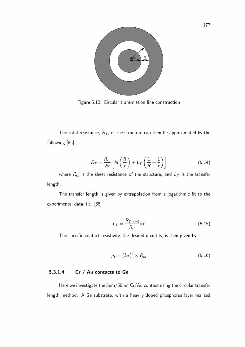
177
R
r d
Figure 5.12: Circular transmission line construction
The total resistance, RT , of the structure can then be approximated by the
following [85]:-
RT =Rsh
2π
[
ln
(
R
r
)
+ LT
(
1
R+
1
r
)]
(5.14)
where Rsh is the sheet resistance of the structure, and LT is the transfer
length.
The transfer length is given by extrapolation from a logarithmic fit to the
experimental data, i.e. [85]
LT =RT |x=0
Rsh
πr (5.15)
The specific contact resistivity, the desired quantity, is then given by
ρc = (LT )2 × Rsh (5.16)
5.3.1.4 Cr / Au contacts to Ge
Here we investigate the 5nm/50nm Cr/Au contact using the circular transfer
length method. A Ge substrate, with a heavily doped phosphorus layer realized
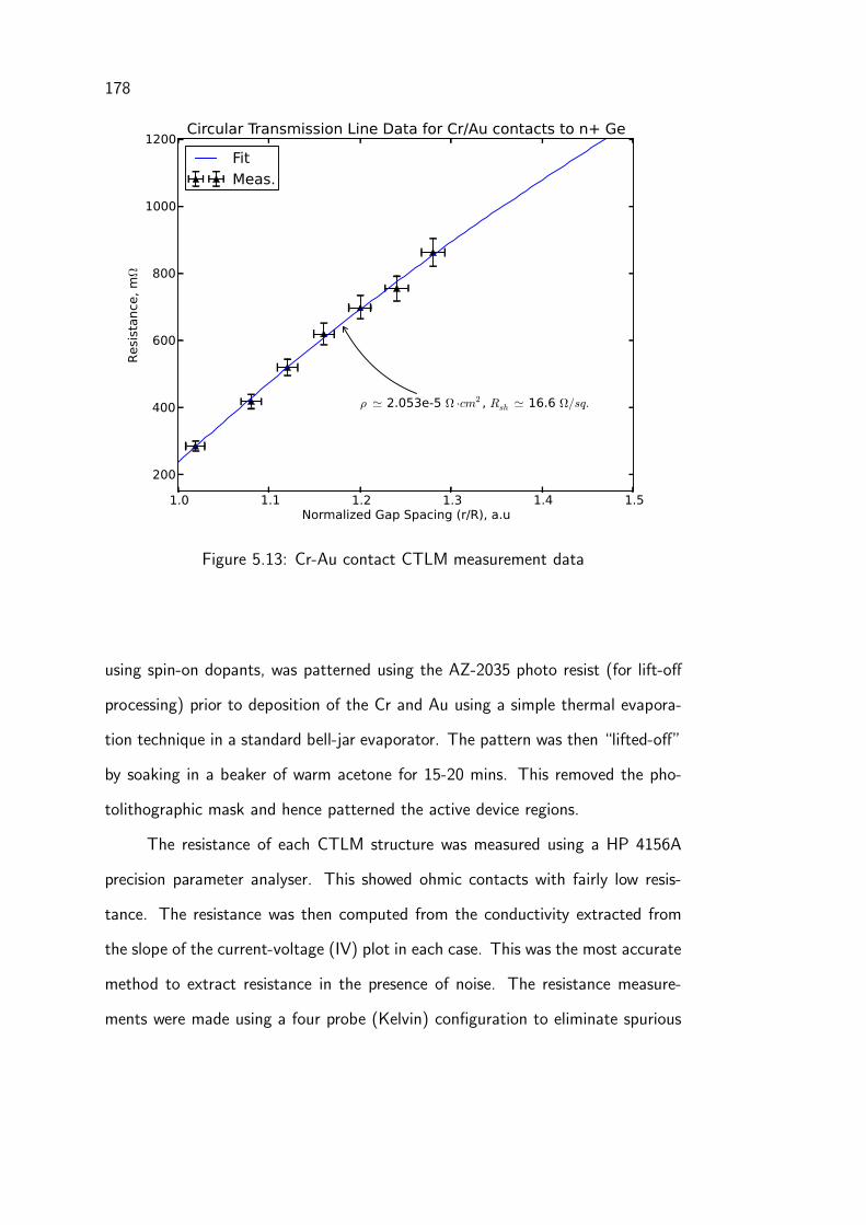
178
1.0 1.1 1.2 1.3 1.4 1.5Normalized Gap Spacing (r/R), a.u
200
400
600
800
1000
1200Resistance, mΩ
ρ ≃ 2.053e-5 Ω ·cm2 , Rsh ≃ 16.6 Ω/sq.
Circular Transmission Line Data for Cr/Au contacts to n+ Ge
FitMeas.
Figure 5.13: Cr-Au contact CTLM measurement data
using spin-on dopants, was patterned using the AZ-2035 photo resist (for lift-off
processing) prior to deposition of the Cr and Au using a simple thermal evapora-
tion technique in a standard bell-jar evaporator. The pattern was then “lifted-off”
by soaking in a beaker of warm acetone for 15-20 mins. This removed the pho-
tolithographic mask and hence patterned the active device regions.
The resistance of each CTLM structure was measured using a HP 4156A
precision parameter analyser. This showed ohmic contacts with fairly low resis-
tance. The resistance was then computed from the conductivity extracted from
the slope of the current-voltage (IV) plot in each case. This was the most accurate
method to extract resistance in the presence of noise. The resistance measure-
ments were made using a four probe (Kelvin) configuration to eliminate spurious
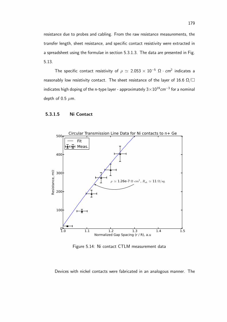
179
resistance due to probes and cabling. From the raw resistance measurements, the
transfer length, sheet resistance, and specific contact resistivity were extracted in
a spreadsheet using the formulae in section 5.3.1.3. The data are presented in Fig.
5.13.
The specific contact resistivity of ρ ≃ 2.053 × 10⁻⁵ Ω · cm2 indicates a
reasonably low resistivity contact. The sheet resistance of the layer of 16.6 Ω/
indicates high doping of the n-type layer - approximately 3×1019cm−3 for a nominal
depth of 0.5 µm.
5.3.1.5 Ni Contact
1.0 1.1 1.2 1.3 1.4 1.5Normalized Gap Spacing (r / R), a.u
0
100
200
300
400
500
Re
sist
an
ce,
mΩ
ρ ≃ 1.26e-7 Ω ·cm2 , Rsh ≃ 11 Ω/sq.
Circular Transmission Line Data for Ni contacts to n+ Ge
FitMeas.
Figure 5.14: Ni contact CTLM measurement data
Devices with nickel contacts were fabricated in an analogous manner. The

180
nickel was deposited directly onto the germanium, this time with e-beam evap-
oration as the deposition technology from pellets of 6N purity Ni using a BOC
Edwards E-beam evaporation system. There followed the usual lift-off patterning
to form the CTLM structures.
These proved to be of such low resistance that the parameter analyzer had
great difficulty performing the measurements accurately. Hence the measured data
does not agree with the model particularly well and the specific contact resistivity
extracted is only of limited accuracy.
Nevertheless the data were processed and the key parameters extracted in an
entirely analogous manner to the foregoing section, which gave a specific contact
resistivity ρ ≃ 1.26 × 10⁻⁷ Ω · cm2. This seems a little optimistic, although
difficulties in fitting the data may be responsible. Additionally, the sheet resistance
of 11 Ω/ would yield a carrier concentration of 6×1019cm−3 for a nominal depth
of 0.5 µm - this seems quite high but still in the range of carrier concentration of
these heavily doped devices that can be reasonably expected. The data are given
in Fig. 5.14.
5.3.1.6 Al contact
Aluminium was deposited using a standard bell-jar evaporation system from
4N Al wire. The devices were processed using lift-off patterning, as in previous
sections.
The rather high specific contact resistivity, ρ ≃ 3.98×10⁻³ Ω ·cm2, is rather
surprising. This indicates that Al did not form a very good contact to the n+ doped
Ge. This may be due to the fact that Al acts as a p-type dopant in Ge. This
could have formed a small barrier at the Al-Ge interface, increasing specific contact
resistivity. The IV characteristics showed slight rectifying characteristics. The sheet
resistance of 18 Ω/ gives an n+ doping concentration of around 2.5×1019cm−3

181
1.0 1.1 1.2 1.3 1.4 1.5Normalized Gap Spacing (r / R), a.u
3400
3450
3500
3550
3600
3650
3700
3750
3800
Resistance, mΩ
ρ ≃ 3.98e-3 Ω ·cm2 , Rsh ≃ 18 Ω/sq.
Circular Transmission Line Data for Al contacts to n+ Ge
FitMeas.
Figure 5.15: Al contact CTLM measurement data
for the nominal sheet thickness 0.5 µm. Again, this seems reasonable. The data
are depicted in Fig. 5.15.
5.3.1.7 Ti contact
Titanium contacts were deposited using the e-beam evaporation system de-
scribed above and patterned using lift-off patterning. The specific contact resis-
tivity of ρ ≃ 1.01×10⁻⁶ Ω ·cm2 is quite low, which indicates a favourable contact.
On the other hand, the sheet resistance of 14.2 Ω/ is again, within the range
expected. The data are shown in Fig. 5.16.
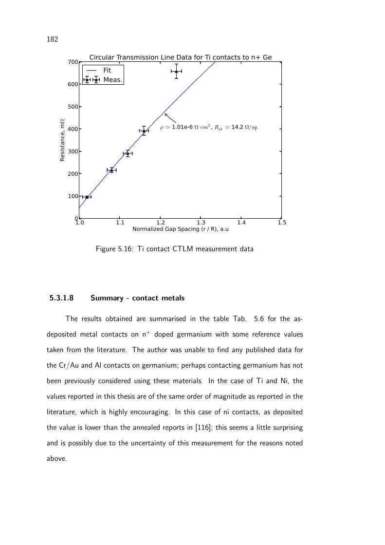
182
1.0 1.1 1.2 1.3 1.4 1.5Normalized Gap Spacing (r / R), a.u
0
100
200
300
400
500
600
700R
esi
sta
nce
, mΩ
ρ ≃ 1.01e-6 Ω ·cm2 , Rsh ≃ 14.2 Ω/sq.
Circular Transmission Line Data for Ti contacts to n+ Ge
FitMeas.
Figure 5.16: Ti contact CTLM measurement data
5.3.1.8 Summary - contact metals
The results obtained are summarised in the table Tab. 5.6 for the as-
deposited metal contacts on n+ doped germanium with some reference values
taken from the literature. The author was unable to find any published data for
the Cr/Au and Al contacts on germanium; perhaps contacting germanium has not
been previously considered using these materials. In the case of Ti and Ni, the
values reported in this thesis are of the same order of magnitude as reported in the
literature, which is highly encouraging. In this case of ni contacts, as deposited
the value is lower than the annealed reports in [116]; this seems a little surprising
and is possibly due to the uncertainty of this measurement for the reasons noted
above.

183
Metal
Specific
contact
resistivity,
Sheet
resistance,
Reference
valueRef.
ρ (Ω · cm2) Rsh (Ω/) (Ω · cm2)
Cr/Au 2.053× 10⁻⁵ 16.6 - -
Ni 1.26× 10⁻⁷ 11 (2.3± 1.8)× 10−7 [116]
Al 3.98× 10⁻³ 18 - -
Ti 1.01× 10⁻⁶ 14.2 7× 10⁻⁷ [118]
Table 5.6: Summary of contact metal parameters
5.4 Conclusions
In this section we investigated the use of ICPECVD films and a combination
of wet and dry treatments to help passivate the sensitive and highly reactive Ge
surface, the use of ICPECVD films and thermally evaporated MgF2 to provide
antireflection capacity, and the use of 4 readily available contact metals to make
low resistance contacts to Ge.
We noted that of the wet and dry treatments, the combination of halide
wet treatment and NH3 dry treatment produced the best results with the lowest
surface recombination velocity for the devices. This indicated that dangling bonds
and interface states were best accounted for with these techniques. This was in
contrast to wet treatment with HF/H2O and hydrogen dry treatment, which did
not perform as well. Interestingly, only the dry NH3 treated, a-Si:H/SiNx capped
sample outperformed the control sample which was only treated with halide wet
chemical treatment. This tends to indicate that other dry pre-treatments either
did not passivate the surface states or even caused surface damage which created
further interface states.
184
Of the AR coatings, the combination of a-Si:H, SiNx and MgF2 was opti-
mised to yield reflection losses below 10%, or to be precise, with minimum reflec-
tivity of 6.47%.
Out of all contact materials to n-type Ge, Ni gave the lowest as-deposited
specific contact resistivity, with Ti and Cr/Au both attractive other options for
low resistance Ge contacts. Al was not a good choice for n+ doped material
due to unintentional doping and consequential barrier formation giving rise to
highly resistive contacts. Calculations for the solar cells presented in the following
chapter assumed a specific contact resistivity of 2e-5 Ohm · cm2 and 100 µm thick
contacts to give a power loss of 0.22% due to I2R losses in the grid bars; this tends
to indicate that all contact materials considered in this chapter with the exception
of aluminium are suitable for use with germanium solar cells, however since lowest
cost would be obtained with a nickel contact, this would be the material of choice.
Chapter 6
Germanium pn-junction devices
6.1 Introduction
In this chapter we investigate germanium pn junction devices. Since the
passivation, antireflection and contacting processes were developed in previous
chapters, these can be combined into a fully featured diode process capable of
creating high quality diode devices with good reproducibility and high yield.
The process is based on mesa etching as opposed to a planar process since
germanium lacks a stable native oxide and, furthermore, there are very few selective
etches between the available field oxides and nitrides. The only material available
to fulfill the role of field oxide is PECVD or spin-on silicon dioxide, which is not
a particularly good diffusion mask. Field oxide or nitride deposition also adds
additional processing steps and extra complexity, which is not desirable for a solar
cell process. Correspondingly it was decided in favour of a mesa etch for the edge
isolation step when designing the process, which is the more usual case for solar
cell fabrication.
One interesting feature of the germanium process is the use of combined AR
coating and reactive ion etching (RIE) etch mask. It was found that the top layer of
the passivation/AR coating (MgF2) was quite resilient to RIE and could be used as
a mask, which removes the necessity of another mask material for this processing
step. Instead, the MgF2 is pre-patterned with lift-off patterning and then the

186
whole sample etched in an RIE to open contact pads prior to contact deposition.
By removing the additional processing step, the process is made simpler and more
manufacturable.
Difficulties processing germanium include its high chemical reactivity and its
brittle mechanical properties. Germanium reacts with most wet etches and espe-
cially with O2/CF4 RIE. Hence wafer cleaning times must be kept to a minimum
and RIE etch rates carefully determined to avoid overetching through device active
regions. There are very few selective etches for Ge which compounds the problem.
The solution is to exercise caution when etching germanium. One must also exer-
cise caution with thin (170 µm thick) solar grade wafers since they are extremely
brittle and prone to shatter or crack if mishandled.
Care must also be taken with exposed mesas since contamination could result
in an inclusion on the edge of the mesa which would cause the device to break
down prematurely. Cleanliness is required during processing and the devices are
given a preclean/etch before passivation to ensure that the mesa edges are free
from defects and inclusions.
6.2 Germanium wafer selection
In this chapter, germanium wafers from three suppliers are considered. There
are several reasons for the choice of wafers. Firstly, the wafers from Sylarus were
the lowest in cost. They were available in 4” format and could be cleaved to
suitably sized samples. However, these wafers were only 170 µm thick; this made
this material very difficult to work with as the samples were quite brittle and prone
to cracking. Hence thicker wafers were sought after. Wafers from University
Wafer were of reasonable cost and much thicker (500 µm) so these were used in
some experiments. However the doping of these wafers (1e15 cm−3) was too low
to be used for solar cell applications (we require based doping of at least 1e17

187
Wafer supplier Thickness Doping Cost Experiments
Sylarus 170 µm 5e17 cm−3 $70 GE095, GE0125
University Wafer 500 µm 1e15 cm−3 $120 GE099
JMP Technology Sarl 300 µm 1e17 cm−3 $250 GE0314, GE0313-2
Table 6.1: Wafers used in this chapter
cm−3 for reasonable open circuit voltage of single junction Ge solar cells) so a
third batch of wafers, from JMP Technology Sarl, was obtained. These were VGF
wafers that sadly despite their cost were of poor quality and contained a great
many crystallographic defects, impairing some experiments. The choice of wafers
for the experiments detailed in this chapter is presented in Tab. 6.1.
6.3 Diode fabrication
6.3.1 Fabrication process
Small samples are first prepared from bulk Ge wafers by scribing with a
diamond scribe and breaking along the scribe lines. Thin Ge wafers (170 µm
thick) cleave very easily but are brittle and prone to cracking. In addition, wafers
supplied with a miscut for III-V solar cell epitaxy were found to cleave along non-
preferred crystallographic axes due to the misorientation. This made things quite
difficult; nevertheless the cleaving process allowed the larger wafers to be divided
into smaller, more manageable, pieces could be handled in the laboratory.
Cleaved samples must be degreased in boiling trichloroethylene, acetone,
and methanol, and subject to ultrasonic bathing to remove any traces of grease
from the wafer sawing process or dust and contaminants from the cleaving process.
Germanium does not react with the solvents but is partially soluble in water so
deionised water rinsing time is kept to a minimum.
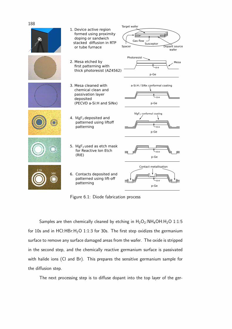
1881. Device active region
formed using proximity
doping or sandwich
stacked diffusion in RTP
or tube furnace
2. Mesa etched by
first patterning with
thick photoresist (AZ4562)
3. Mesa cleaned with
chemical clean and
passivation layer
deposited
(PECVD a-Si:H and SiNx)
4. deposited and
patterned using liftoff
patterning
6. Contacts deposited and
patterned using lift-off
patterning
5. used as etch mask
for Reactive Ion Etch
(RIE)
Gas flow
Dopant source
wafer
Susceptor
Target wafer
Spacer
Photoresist
Mesa
p-Ge
n+
a-Si:H / SiNx conformal coating
p-Ge
n+
p-Ge
n+
p-Ge
n+
p-Ge
n+
Contact metallisation
Figure 6.1: Diode fabrication process
Samples are then chemically cleaned by etching in H2O2:NH4OH:H2O 1:1:5
for 10s and in HCl:HBr:H2O 1:1:3 for 30s. The first step oxidizes the germanium
surface to remove any surface damaged areas from the wafer. The oxide is stripped
in the second step, and the chemically reactive germanium surface is passivated
with halide ions (Cl and Br). This prepares the sensitive germanium sample for
the diffusion step.
The next processing step is to diffuse dopant into the top layer of the ger-

189
manium sample to form the device active region. For example, this could be n+
dopant diffused into a p-type wafer for an n-on-p process. Diffusion is from spin-on
dopant sources and can be performed using either direct spin-on doping, proximity
doping, or “sandwich-stacked” diffusion.
If the sample is directly spun with dopant solution, an extra processing step
is required to strip the spin-on dopant film. This adds extra processing time and
complexity. Additionally, if the spin-on dopant film is directly adhered to the
wafer, any contaminants in the spin-on dopant matrix can diffuse into the sample,
impairing lifetime. For example the spin-on dopants may contain lifetime impairing
impurities such as iron and copper.
Another issue impairing the direct spin-on approach is small defects in the as-
spun layer. These are caused by aging of the phosphorus spin-on dopant film which
over time starts to form lumps of silica gel. These defects and inhomogeneities
will propagate to the doped layer forming an inhomogeneous active region. This
has the potential to cause premature breakdown or complete failure in devices and
is to be avoided.
Correspondingly the preferred method for emitter formation is by the prox-
imity doping method. In this method the extra processing step to remove spin-on
dopant film is no longer required, however there is some additional sample prepa-
ration necessary to prepare the SOD source wafer. Since the SOD source wafer
is pre-outgassed to remove contaminants prior to diffusion, the issue of contam-
ination is circumvented. Since the doping occurs by a vapour transport process,
this issue of striations and defects in the SOD film causing an inhomogeneous ac-
tive region is also circumvented. Hence the proximity doping process is the more
reliable process for device fabrication.
To isolate the edges of the active region and define the device, a mesa etch
step follows. The isolation mesa etches are performed using H2O2:NH4OH:H2O

190
1:1:20. This consumes Ge at a rate of 233 nm/min. To prevent potential degra-
dation of the photoresist in this solution (which is basic and acts like photoresist
developer) a thick photoresist such as AZ4562 is necessary. This allows for the
photoresist to maintain its integrity throughout the etch process even allowing
for gradual etching of the resist mask. The mesa etches are performed for long
enough to completely isolate the device, i.e. at least 5 minutes, which removes
over a micron of material.
After mesa etch, the samples are prepared for passivation deposition by a
chemical clean. This consists of a dip etch in NH4OH:H2O2:DI 1:1:5 for 30s to
remove any surface damage and clean away any potential impurities and inclusions
on the sensitive mesa boundary, and a soak for 1 minute in 1:1:5 HCl:HBr:DI to
remove any surface oxide and terminate the surface with Cl and Br ions.
The diode under construction is then loaded into the ICPECVD chamber and
exposed to ammonia gas at 250 C . This is the dry pre-treatment stage of the
passivation process outlined in chapter 5. The ammonia gas pre-treatment serves
to passivate in situ in the deposition chamber any dangling Ge bonds with either
nitrogen or hydrogen. The advantage of in-situ treatment is obviously the process
is performed under vacuum with no exposure of the Ge surface to the atmosphere
prior to passivation layer deposition.
Next, 10 nm of a-Si:H followed by 60 nm high quality SiNx are then confor-
mally deposited on the sample which passivates the mesa boundary and conformally
coats the entire sample surface. The sample should be terminated with H and N
so the surface should feature Ge-N-Si and Ge-H bonds. This should adequately
passivate the sensitive germanium surface and yield a robust device which can
handle subsequent processing without risk of damage.
MgF2 is now deposited by a simple thermal evaporation process. Care must
be taken when thermally evaporating MgF2 since it undergoes a phase transition at

191
1263 C to liquid phase. This temperature is similar to the temperature reached
by the boat during evaporation. As a liquid, the rate of MgF2 evaporation is
significantly higher than as a crystalline solid. Hence the deposition thickness
may become difficult to control if the deposition rate spontaneously increases by
a large amount. This necessitates careful control of the deposition rate and time
to minimize the chance of a spontaneous phase transition.
The MgF2 is patterned using liftoff patterning. This is the only available
option for MgF2 patterning since MgF2 is chemically resistant to most acids, bases,
and RIE. Since the melting point of MgF2 is quite low the deposition should not
occur at elevated temperatures (i.e. due to substrate heating radiatively from the
boat) so the use of a thin negative photoresist like AZ2035 is possible.
The next processing step is RIE. RIE is carried out in an Oxford Instruments
Plasmalab Plasma 100 reactive ion etch. The etch used is O2/CF4 which consumes
both SiNx and a-Si:H but leaves MgF2 intact. However, the RIE process also
consumes Ge, and more importantly, at an extremely high etch rate. Hence the
process has to be appropriately timed to prevent over-etching the germanium and
damaging the device active layer. Since the RIE process does not attack the
MgF2 significantly, the sample can simply be taken from the lift-off patterning
step directly to the RIE since there is no need for additional masking. This saves
a processing step.
Contacts are deposited again using thermal evaporation and lift-off pattern-
ing. The lowest resistance contact to Ge is with nickel metal. This can be thermally
evaporated or alternatively e-beam evaporated. Contacts can be annealed at 250
C to further improve contact resistance.
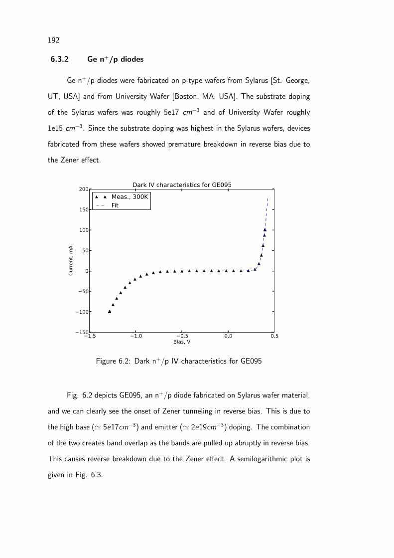
192
6.3.2 Ge n+/p diodes
Ge n+/p diodes were fabricated on p-type wafers from Sylarus [St. George,
UT, USA] and from University Wafer [Boston, MA, USA]. The substrate doping
of the Sylarus wafers was roughly 5e17 cm−3 and of University Wafer roughly
1e15 cm−3. Since the substrate doping was highest in the Sylarus wafers, devices
fabricated from these wafers showed premature breakdown in reverse bias due to
the Zener effect.
−1.5 −1.0 −0.5 0.0 0.5Bias, V
−150
−100
−50
0
50
100
150
200
Curr
ent,
mA
Dark IV characteristics for GE095
Meas., 300KFit
Figure 6.2: Dark n+/p IV characteristics for GE095
Fig. 6.2 depicts GE095, an n+/p diode fabricated on Sylarus wafer material,
and we can clearly see the onset of Zener tunneling in reverse bias. This is due to
the high base (≃ 5e17cm−3) and emitter (≃ 2e19cm−3) doping. The combination
of the two creates band overlap as the bands are pulled up abruptly in reverse bias.
This causes reverse breakdown due to the Zener effect. A semilogarithmic plot is
given in Fig. 6.3.

193
The model fit to the data in Fig. 6.2 is a simple two diode model. The
parameters of the fit are n1 = 1.0, n2 = 2.0 (ideality factors of the two diodes), A
= 0.01131 cm2 (area), J0,1 = 4e-6 A/cm2, J0,2 = 3e-4 A/cm2 (saturation current
densities), Rs = 0.21 Ω (series resistance), and Rp = 3e3 Ω (shunt resistance).
The ideality factor n1 being exactly 1.0 indicates a reasonably high quality
crystalline wafer with a long bulk lifetime was used. Consequently the diode itself is
of reasonable quality. If the device were fabricated on a poor quality wafer we would
expect to see a higher saturation current for the second diode of our two diode
model and the ideality factor of the first diode higher than 1.0. An ideality factor
higher than one indicates a low quality junction and is indicative of recombination
losses [119]; an ideality factor approaching 2.0 is found if generation-recombination
in the space charge region is significant and shallow traps close to the intrinsic
level are present [119]. In our case we can see that generation-recombination is
not significant and there is not a high density of mid-gap defects.
In contrast, the n+/p junction GE099 was fabricated on low doped University
Wafer material. This gave no premature Zener breakdown in reverse bias since
the substrate doping (roughly 1e15 cm−3) is simply too low. Reverse breakdown
occurred instead at -25V or greater (i.e. more negatively biased). This breakdown
may be due to avalanche effect or potentially Zener tunneling; it is unclear which
from the characteristics themselves but Zener tunneling seems more likely since
the breakdown characteristics are not particularly abrupt. This device is shown in
Fig. 6.4 and Fig. 6.5.
Considering the log-linear plot of the IV characteristics of GE099, we see a
reasonable fit to the measurements with a simple two diode model. The fitting
parameters were n1 = 1.0, n2 = 1.16, A = 0.01131 cm2, J0,1 = 1e-6 A/cm2, J0,2
= 4.8e-4 A/cm2, Rs = 1.1 Ω, and Rp = 1e5 Ω. The comparatively high shunt
resistance and low ideality factor (n1 = 1.0) highlight the quality of the junction.

194
−0.4 −0.2 0.0 0.2 0.4Bias, V
10-6
10-5
10-4
10-3
10-2
10-1
100
Curr
ent,
A
Dark IV characteristics for GE095
Meas., 300KFit
Figure 6.3: Dark n+/p IV characteristics for GE095 - logarithmicscale
−1.5 −1.0 −0.5 0.0 0.5Bias, V
−20
0
20
40
60
80
100
Curr
ent,
mA
Dark IV characteristics for GE099
Meas., 300KFit
−25 −20 −15 −10 −5 0 5−10
0
10
20
30
40
50
60
Figure 6.4: Dark IV characteristics for GE099

195
We may compare the fitted results for GE095 and GE099 to published data.
Wang et al. [120] report a Si:Ge solar cell fabricated with over 90% Ge content;
they report n1 = 1.0, n2 = 2.0, J0,1 = 1.3e-4 A/cm2, J0,2 = 1.0e-7 A/cm2, Rs =
0.5 Ω·cm2, and Rp = 1e5 Ω·cm2. The higher saturation current density (by almost
two orders of magnitude) is indicative of the poorer quality material resulting from
thin film RPCVD (reduced pressure chemical vapour deposition) which no doubt
will yield poorer lifetimes as compared to our bulk wafers. Our devices show better
series resistance characteristics but poorer shunt resistance. The shunt resistance
is no doubt due to pin hole defects in the spin-on dopant films causing small
conductive paths through the junction. Since our extracted parameters are for
the most part better than those reported in [120] we can expect higher conversion
efficiency for solar cells using this diode process than that reported in [120] (0.79%
efficiency at 30 suns). To further improve efficiency we would need to increase
bulk lifetime (reducing J0,1 and J0,2) and increase Rp.
6.3.3 Ge n+/p+ “tunnel” diode
A heavily doped n+/p+ diode was fabricated by diffusing into pre-prepared
Ga p+ doped material using standard direct spin-on phosphorus SOD film. The Ga
doping was performed using the sandwich-stacked diffusion technique. Gallium was
diffused and driven in until the profile had a surface concentration of approximately
1e19 cm−3 as estimated from the model derived in section Section 4.6.1. The
resultant diode had very early onset of Zener tunneling, which showed that both
emitter and base doping were quite high. However, not high enough, or abrupt
enough, to realise an Esaki diode. The diode was measured at 300K and 80K.
Diode IV characteristics are shown in Fig. 6.6.
The hump of excess current shown at 80K is most likely the onset of tunneling
processes within the diode at 80K as the band alignment becomes more favourable

196
−0.4 −0.2 0.0 0.2 0.4Bias, V
10-8
10-7
10-6
10-5
10-4
10-3
10-2
10-1
Curr
ent,
A
Dark IV characteristics for GE099
Meas., 300KFit
Figure 6.5: Dark IV characteristics for GE099, logarithmic plot
−0.8 −0.6 −0.4 −0.2 0.0 0.2 0.4 0.6 0.8Bias, V
10-5
10-4
10-3
10-2
10-1
100
101
102
Curr
ent,
A
Dark IV characteristics for GE0313-2
Meas., 300KMeas., 80K
Figure 6.6: Dark IV characteristics for GE0313-2, logarithmicplot

197
due to kT becoming smaller [65]. However, there is not enough tunneling current
to allow the device to be called a true tunnel diode.
Since the device is passivated with a PECVD silicon dioxide film, it is unlikely
that lateral defects or inclusions play a role in the breakdown characteristics of this
“tunnel diode”. Its characteristics are purely due to the Zener effect due to heavy
doping either side of the junction, since CV profiling confirmed a narrow depletion
width and heavy doping of the base region.
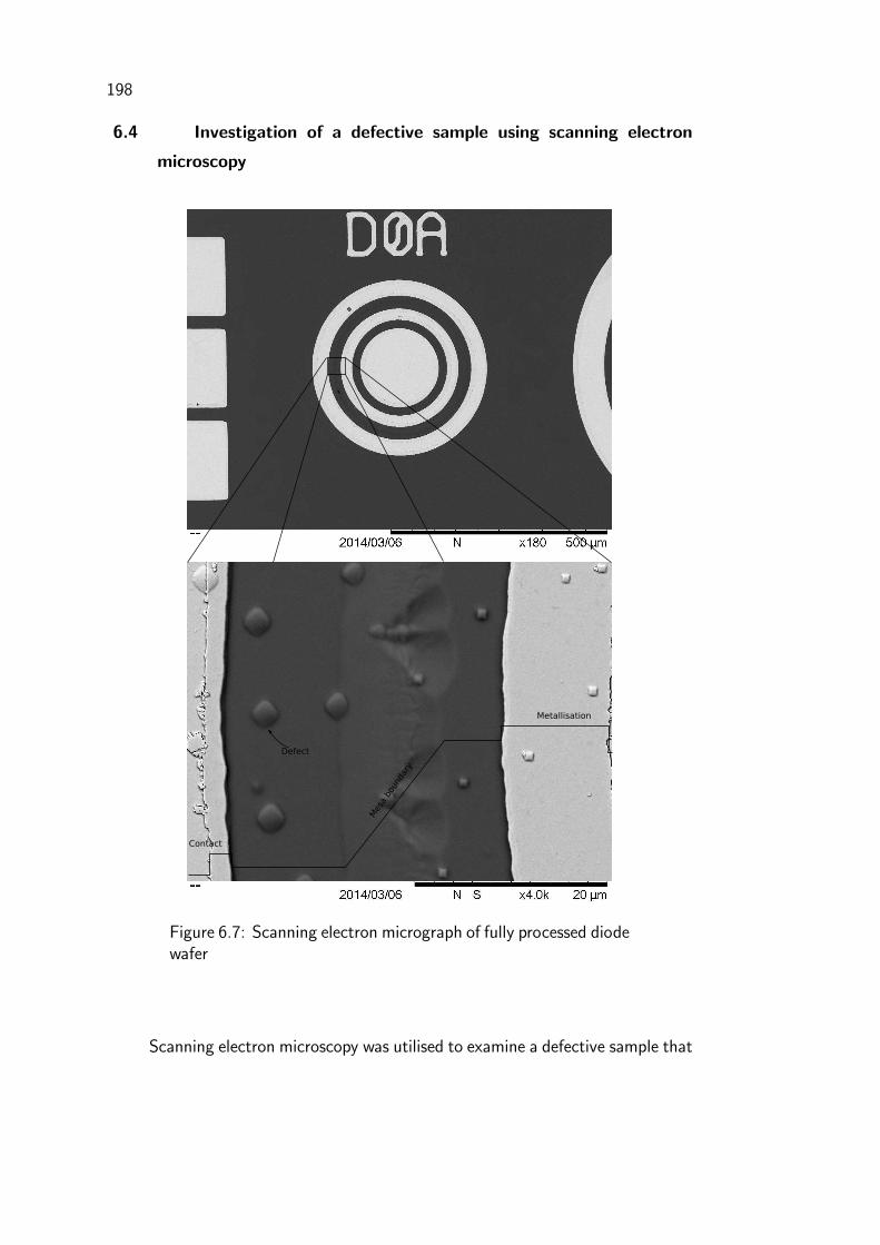
198
6.4 Investigation of a defective sample using scanning electron
microscopy
Mesa
boundary
Metallisation
Contact
Defect
Figure 6.7: Scanning electron micrograph of fully processed diodewafer
Scanning electron microscopy was utilised to examine a defective sample that

199
had been fabricated from vertical gradient freeze (VGF) wafers supplied by JMP
Technology Sarl [Porrentruy, Switzerland]. It is possible that the high temperature
ramp rate and associated mechanical stress resulted in recrystallisation of the VGF
wafers during the diffusion process, which caused a great many defects to nucleate
in the wafer. These defects are visible under the scanning electron microscope at
high magnification.
Fig. 6.7 shows a close up of the diode mesa. The defects are clearly visible,
both on the surface, where they are approximately 1 micron in size and square-
shaped, and in the etched trough outside the mesa boundary, where they are
diamond shaped and closer to 3-4 microns in size, and also on the mesa itself,
where the defect leaves two etch pits in its wake along the mesa edge.
Staining is also present down the edge of the mesa. This is due to high
phosphorus content staining the germanium during etching due to the dissimilar
etch rates between gallium and phosphorus doped germanium. This staining can
be used to identify the junction depth. For example, as viewed directly from above
the stained region is 2.5 microns in distance. This projected down the 54.76 degree
slope made by the < 111 > glide plane gives a junction depth of roughly 1.8 µm.
6.5 Germanium solar cells
Before the process described Section 6.3.1 was developed, a number of trial
processes were experimented with. The process in Section 6.3.1 was arrived at
through these experiments, which sought to optimise process parameters to obtain
higher yield and better quality devices. One such initial process was used to create
a solar cell of rather poor efficiency.
This solar cell (GE0125) was prepared by cleaving and cleaning a 1cm x 1cm
piece of Ge wafer supplied by Sylarus [St. George, UT]. The sample was then
masked using spin-on glass which was patterned using HF etching. This formed

200
0.00 0.02 0.04 0.06 0.08 0.10 0.12 0.14 0.16 0.18Bias, V
−14
−12
−10
−8
−6
−4
−2
0C
urr
ent
densi
ty, J, mA/cm
2Illuminated IV and PV characteristics for GE0125
J, Meas.−1.0
−0.8
−0.6
−0.4
−0.2
0.0
Pow
er,
P, m
W
Voc: 159 mV Jsc: 12 mA/cm2 FF: 54.50% η: 1.0%
P, Meas.
Figure 6.8: GE0125, illuminated IV and PV characteristics
the diffusion mask by which the active region was formed. The device active region
was then formed by direct spin-on doping the sample and diffusing at 650C for
10 minutes. The spin-on glass was not removed after the process but instead left
on the device as a combined passivation/antireflection coating. This layer was
then patterned for contact formation, and contacts were deposited and defined via
lift-off.
The IV and PV characteristics of this cell are depicted in Fig. 6.8. Without
the many optimisations leading up to the process outlined in Section 6.3.1, the
results are fairly poor. The device is 1% efficient and has a short circuit current
density of 12 mA/cm2. This poor short circuit current density is most likely due to
the phosphorus doped spin-on glass film used as a passivation layer reflecting and
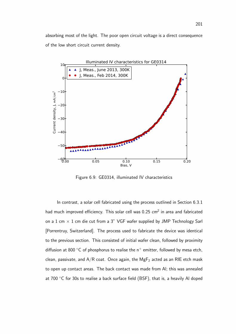
201
absorbing most of the light. The poor open circuit voltage is a direct consequence
of the low short circuit current density.
0.00 0.05 0.10 0.15 0.20Bias, V
−60
−50
−40
−30
−20
−10
0
10
Curr
ent
densi
ty, J, mA/cm
2
Illuminated IV characteristics for GE0314
J, Meas., June 2013, 300KJ, Meas., Feb 2014, 300K
Figure 6.9: GE0314, illuminated IV characteristics
In contrast, a solar cell fabricated using the process outlined in Section 6.3.1
had much improved efficiency. This solar cell was 0.25 cm2 in area and fabricated
on a 1 cm × 1 cm die cut from a 3” VGF wafer supplied by JMP Technology Sarl
[Porrentruy, Switzerland]. The process used to fabricate the device was identical
to the previous section. This consisted of initial wafer clean, followed by proximity
diffusion at 800 C of phosphorus to realise the n+ emitter, followed by mesa etch,
clean, passivate, and A/R coat. Once again, the MgF2 acted as an RIE etch mask
to open up contact areas. The back contact was made from Al; this was annealed
at 700 C for 30s to realise a back surface field (BSF), that is, a heavily Al doped

202
0.00 0.05 0.10 0.15 0.20Bias, V
−9
−8
−7
−6
−5
−4
−3
−2
−1
0Pow
er
densi
ty, P, mW/cm
2
June 2013, Voc: 194 mV Jsc: 54 mA/cm2 FF: 51.71% η: 5.4%
Feb 2014, Voc: 190 mV Jsc: 52 mA/cm2 FF: 54.32% η: 5.3%
Illuminated PV characteristics for GE0314
P, Meas., June 2013, 300KP, Meas., Feb 2014, 300K
Figure 6.10: GE0314, illuminated PV characteristics
Ge region that serves to reflect minority carriers and only allow majority carrier
holes to recombine at the back surface. Front contacts were made from Cr and
thick gold, however, the gold could not be made thick enough (only 200-300 nm)
for low contact resistance of the finger pattern. Hence the contact resistance was
higher than expected (this manifested itself as a series resistance of ≃ 1 Ohm).
The measured parameters for this cell were JSC = 54 mA, Voc = 194 mV, η =
5.4%, FF = 51.7%. The IV characteristics for this cell are shown in Fig. 6.9 and
the PV characteristics are depicted in Fig. 6.10.
It was a pleasing result that the device had identical characteristics when
remeasured again almost 9 months later. When remeasured in February 2014, the
device performed almost identically with measured parameters JSC = 52 mA, Voc

203
= 190 mV, η = 5.3 %, FF = 54.3%. The device had not been kept in a controlled
environment nor subjected to any particular environmental controls (such as tem-
perature, humidity, etc). This indicates that the storage stability of the devices
is quite good and the passivation technology serves as an excellent environmental
passivant protecting the sensitive devices from moisture and atmospheric contam-
inants.
Given what was seen in Section 6.4, the high number of defects in the wafers
supplied by JMP Technology Sarl are the most likely cause of the low efficiency of
this device. These defects act as recombination centers and lower the bulk lifetime
in the device, impacting on open circuit voltage, short circuit current density, and
fill factor. The fill factor is also adversely affected by series and shunt resistance
in this device. The shunt resistance may be attributable to defects in the dopant
source film, which become more significant due to the larger area of the device,
or potentially to lateral defects and inclusions (such as the precipitates seen in
Section 6.4). It is unclear which mechanism is responsible for the shunt resistance.
Series resistance on the other hand is marred by thin contact films for the top
contact. These films need to be microns thick, however using a simple thermal
evaporation process, only hundreds of nanometers are practical. Technologies for
thicker contact deposition such as screen printing or electrodeposition need to be
investigated.
It is interesting to compare the two solar cell devices and attribute the effi-
ciency gain to various key process technologies developed in the previous chapters.
Firstly, GE0304 is 10 times the area of GE0125. This shows the improvement in
processing due to the use of proximity doping that allows the area to be scaled.
The improvement in short circuit current density (54 as opposed to 12 mA/cm2) is
due to the improvement of the passivation and antireflection technology developed
in chapter 5.

204
6.6 Conclusions
In this section a fully featured process for diode fabrication was presented.
The process consists of 6 basic processing steps and can move through a small
laboratory scale foundry, such as the A.G Nassibian Nanofabrication Facility at the
University of Western Australia, in under a week.
The process was well suited to use of proximity doping or sandwich stacked
diffusion for device fabrication. It was concluded that either of these techniques
were preferable to direct spin-on doping of the substrate to prevent diffusion of
impurities as well as process related defects such as influence of precipitates, small
bubbles, and radial striations which can come about as the dopant films approach
their shelf-life.
Process novelties included the use of MgF2 as a combined AR coating and
etch mask due to the high chemical inertness of MgF2 and its resistance to reac-
tive ion etching. This allowed a processing step to be removed saving time and
simplifying the process.
Out of the many diodes fabricated, two of particular quality were chosen to
be indicative of the potential for this process. These diodes had reasonable IV
characteristics including ideality factors close to 1 showing high quality crystalline
substrates with few defects and long bulk lifetimes. Diodes fabricated on epi-
ready solar-grade wafers showed early breakdown due to the Zener effect. Since
these substrates were intended for solar cell application, the substrate doping was
a nominal 5 × 10¹⁷. This is suitably high for early onset of Zener tunneling in
a moderate bandgap material such as germanium. Devices fabricated on lower
doped substrates showed much higher breakdown, at around 25V. This breakdown
could be due to the avalanche effect due to the high field at such voltages, or
Zener tunneling. It is difficult to discern which effect causes the breakdown from

205
the characteristics directly.
SEM was used to investigate precipitate-like defects on a fully processed
diode die. The size of the defects was quite considerable and the defects propa-
gated with the mesa etch process and became enlarged with etch depth. These
defects are thought to be the result of partial recrystallisation of the germanium
wafer during the doping process, which occurs at high temperatures with fast tem-
perature ramp rates. It can be concluded that the VGF wafers were simply of too
poor quality to realise high-performance devices and alternative wafer suppliers
should be considered.
Utilising both n and p type doping, a “tunnel” diode was fabricated. This
did not display the onset of tunnelling in forward bias but did show temperature
dependent changes. Unfortunately, the diode was not heavily doped enough on
the p-side, due to difficulty matching the highly degenerate Ga doping and the
phosphorus spin-on doping, which have different solubilities. For example, the Ga
sample had to be driven in to give the desired doping profile, i.e. surface concen-
tration of 1 × 1019 cm−3, so that the phosphorus doping could fully compensate
and exceed this concentration. However since the Ga doping level at the cross-over
point (where the n-type doping concentration no longer exceeds the p-type doping
concentration) may not necessarily be high enough due to the curvature of the
Gaussian driven-in profile and the unpredictable depth of the phosphorus diffusion,
the overall band bending at the junction may not be sufficient to realise a true
Esaki tunnel diode. This necessitates careful process control and optimisation in
order to balance the two simultaneous doping processes.
A solar cell was fabricated using the diode process. This was a large area
device, with an active area 0.25 of cm2. This demonstrates the applicability of
the process to larger area devices, the use of proximity doping, and the high
quality passivation technology working together to allow for high yield in spite

206
of the larger diode area. In general, the probability of catastrophic failure of a
device scales with area since there is a higher probability of a defect affecting
a critical part of the device, such as mesa or contact pad. The solar cells had
reasonable efficiency for germanium devices, however the efficiency was quite low
compared to other results in the literature. We may conclude that the wafer used
for the device was sub-optimal. Since the VGF wafers were examined by SEM
and found to be highly defective, particularly after partial recrystallisation during
the diffusion process. These defects most likely caused severe degradation of the
bulk lifetime in the device, as well as affected surface recombination velocities,
since these defects propagated to the surface, and cannot be passivated due to
the nature of the defect. This would explain the poor efficiency of the device.
This is somewhat saddening, since budget constraints and the high cost of bulk
germanium forced this particular choice of wafer. It is therefore possible that future
work could investigate the use of higher quality wafers and this process to yield
higher efficiency devices.
The solar cell GE0314 had near identical characteristics when remeasured,
almost 9 months after initial fabrication. This highlighted the storage stability
of the passivated diodes and the effective environmental passivation of the a-
Si:H/SiNx/MgF2 coating. This is due in part to the high chemical inertness of the
MgF2 which does not react with atmospheric contaminants.
It is regrettable that some of the most important experiments in this chapter
were performed with poor quality wafers. The poor efficiency and fill factor of
GE0314 illustrate the poor nature of the JMP Technology Wafers. Unfortunately
time and budget did not permit fabrication of solar cells with better quality wafers
to fully investigate the efficiency improvement offered by the passivation and anti-
reflection technology developed in this work. This is left to future work to elucidate
further. It is recommended that wafers from one supplier are used in comparison

207
experiments in future work to draw the most meaningful conclusions.
It can be concluded that the diode process is highly successful with high
yield and excellent storage lifetime of devices. It is a versatile process that is
equally suited to small signal Ge diode creation as well as photodiode and solar
cell fabrication. It is envisaged that a variety of germanium optoelectronic devices
could be fabricated with this process, and since both n and p type doping has
been demonstrated in this work using a low cost technology, it may be possible to
extend the process further, adding processing steps for formation of three terminal
devices such as bipolar junction transistors.

Chapter 7
II-VI/Germanium Materials Growth and Heterojunction Optoelectronic
Devices
7.1 Introduction
In the context of this work, several growth techniques were developed to
investigate the potential for combination of single crystal germanium with either
single crystal or polycrystalline II-VI materials in either monolithic or mechanically
stacked configuration for use in optoelectronic devices. However, it needs to be
noted that no II-VI materials are directly compatible with germanium, neither in
terms of lattice spacing, nor materials compatibility (since germanium is a compar-
atively reactive substance), nor for that matter in terms of favourable heterojunc-
tion electronic properties. This is of course, in direct contrast to III-V materials,
which are very similar in lattice constant, have very favourable electronic properties
for forming heterojunction devices, and for which materials growth technologies
are mature and well established.
To ameliorate these compatibility issues, we discuss herein the use of an-
other material, namely sapphire, as substrate for materials growth. This substrate
has the advantage of high optical transparency, comparatively low cost, excellent
mechanical properties and a high degree of chemical inertness.
In this section we present the results of materials growth of ZnTe and CdTe
on both sapphire and germanium using thermal evaporation and molecular beam

209
epitaxy (MBE). We also present a CdTe/Ge heterostructure and measure both
current-voltage (IV) and capacitance-voltage (CV) characteristics in order to de-
termine the electronic properties of the interface. The purpose is to pave the way
for monolithic CdTe/Ge tandem solar cells by addressing the materials challenges
associated with group II-VI/IV heteroepitaxy and confirming electronic properties
to assist in further modelling of CdTe/Ge solar cells.
7.2 Choice of materials and crystallography
7.2.1 Introduction
Group II-VI compound semiconductor materials have found application for
use in optoelectronic devices such as infrared detectors, radiation detectors, and
LEDs. However, despite numerous possible applications, the II-VI material sys-
tem is in general less utilized and correspondingly less well understood than other
materials systems such as group IV (Si, Ge, SiC) and group III-V and III-nitride
semiconductors (InGaAs, InGaP, AlGaAs, GaAs, GaN, InGaN etc. etc.) which
have widespread commercial application. Out of all possible group II and group
VI materials (Hg, Cd, Mg, Mn, Te, Se, S, O etc.) we choose to focus on stoichio-
metric ZnTe and CdTe for simplicity. In principal, an alloy of these two materials
(i.e. Zn1−xCdxTe) could be used to tune lattice spacing and electronic properties
(such as forbidden gap) for a particular application over a wide range of values, as
discussed herein.
We now consider some basic principles of crystal systems in order to under-
stand the crystal structure of the materials we are interested in (CdTe, ZnTe, Ge
and sapphire) and introduce fundamental properties needed to characterise these
materials using x-ray diffraction (XRD), presented later in this chapter.

210
7.2.1.1 Space groups and Crystal Systems
In order to create a semiconducting thin film or bulk crystal, atoms must
be arranged in a periodic formation which gives rise to the optical and electronic
properties desirable for a particular application. There are only a limited number
of distinct kinds of crystallographic arrangements possible, which are called crystal
systems. Furthermore, there are a limited number of unit cell configurations termed
Bravais lattices (14 in all). These Bravais lattices are given initials to describe the
class of lattice (e.g. F = face centred cubic, B = body centred cubic, P = primitive,
etc.). In this chapter we primarily concern ourselves with face centred cubic (F)
Bravais lattices, although the rather special case of sapphire is also considered.
Space groups describe a set of crystallographic operations which when ap-
plied to a crystal lattice produce the lattice itself. That is, space groups define a
series of operations such as translations, rotations, and mirroring, which no matter
how many times they are applied simply reproduce or extend the original lattice.
Hence the operations of an infinite lattice’s space group on itself would in fact pro-
duce no effect, i.e., the lattice would be invariant with respect to such operations
[121].
7.2.1.2 The Stereographic Projection
The stereographic projection, or cartographer’s projection, is of particular
usefulness to visualise space groups. It is also invaluable in working with miscut
or misaligned wafers to determine the correct pole, as evidenced below in our
discussion of Ge substrates.
The projection is computed by placing directions on the unit sphere (i.e. by
normalization) and tracing a line from the pole through the direction as located
on the surface of the sphere through the imaging plane as described in Fig. 7.1.

211
S
N
P1
O
P2
N
P1'
P2'
O
Equatorial
plane of
Projection
Small circle on sphere
Small circle in
plane of projection
Small circle in
plane of projection
Figure 7.1: Stereographic projection, after Hammond [122]
7.2.2 Materials science of CdTe/ZnTe/Ge/sapphire
7.2.2.1 Crystal system, phase, structure, and lattice spacings
In this chapter we consider 4 main materials, namely CdTe and ZnTe, as
potential low-cost wide bandgap semiconductor materials for use in optoelectronic
devices, and Ge and sapphire, as potential substrates for thin film deposition. The
crystal systems, phases, structures and lattice parameters are tabulated in Tab.
7.1.
We consider now each material in turn and elucidate the precise nature of

212
Material Phase Crystal system Space GroupLattice
Parameters
Sapphire α− Al2O3 Trigonal - Hexagonal R 3ca = 4.76 A,
c = 12.99 A
CdTe Cubic Cubic (Zincblende) F 43m a = 6.48 A
ZnTe Cubic Cubic (Zincblende) F 43m a = 6.1 A
Ge Cubic Cubic (Diamond) Fd3m a = 5.66 A
Table 7.1: Materials properties for materials in this work ([2],[123])
each as relevant to this work.
7.2.2.2 Sapphire - R-plane
As noted in Tab. 7.1, sapphire belongs to the trigonal-rhombohedral crystal
system, and possesses a rhombohedral unit cell. However, rather paradoxically,
symmetry within the lattice produce a number of other possible ”facets”, of which
there are two hexagonal prisms. The coordinate system within the sapphire lattice
is therefore hexagonal, with two axes of equal length a with angular separation
120 and a third axis of length c perpendicular to the other axes. The lattice
constants a and c are tabulated in Tab. 7.1.
Although when dealing with other kinds of lattices (i.e. cubic), a set of
3 Miller indices is all that is required, in order to promote interchangeability of
crystallographically equivalent directions when dealing with hexagonal lattices, a
set of 4 indices is often used, with the introduction of a fourth crystallographic
axis, as described in Fig. 7.2 [124]. The four indices 〈hki · l〉 are chosen such that,
by geometry,

213
Figure 7.2: Crystallographic axes of sapphire, in the C-plane
i = −(h + k) (7.1)
where 〈hk · l〉 are conventional Miller indices. This ensures that, for example,
the directions 〈101 · 2〉, 〈101 · 2〉, 〈110 · 2〉, 〈110 · 2〉, 〈011 · 2〉, 〈011 · 2〉 and
〈110 · 2〉 which are crystallographically equivalent have interchangeable indices
(and are simply equivalent to 〈01 · 2〉 in rhombohedral coordinates). This system
is sometimes referred to as ”hexagonal Miller indices”.
The principal crystallographic planes of sapphire (or indeed any hexagonal
crystal system) are the C, a, and R planes, as noted in Fig. 7.3.
Figure 7.4 is the stereographic projection for R-plane sapphire.
7.2.2.3 CdTe / ZnTe
Cadmium telluride (CdTe) and zinc telluride (ZnTe) belong to the II-VI
family of semiconducting materials, by virtue of the fact that Cd and Zn both
belong to group II of the periodic table, with Te belonging to group VI. Both
materials have cubic and hexagonal phases, however in this work we only consider
zincblende (cubic) structures.
We concern ourselves with three orientations in this work. These are 〈100〉,
〈111〉, and 〈211〉. The 〈211〉 orientation is important for growth of the material
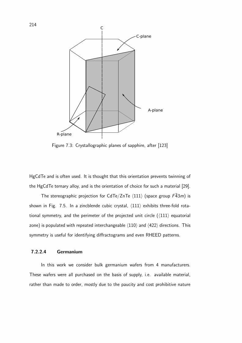
214C
R-plane
A-plane
C-plane
Figure 7.3: Crystallographic planes of sapphire, after [123]
HgCdTe and is often used. It is thought that this orientation prevents twinning of
the HgCdTe ternary alloy, and is the orientation of choice for such a material [29].
The stereographic projection for CdTe/ZnTe 〈111〉 (space group F 43m) is
shown in Fig. 7.5. In a zincblende cubic crystal, 〈111〉 exhibits three-fold rota-
tional symmetry, and the perimeter of the projected unit circle (〈111〉 equatorial
zone) is populated with repeated interchangeable 〈110〉 and 〈422〉 directions. This
symmetry is useful for identifying diffractograms and even RHEED patterns.
7.2.2.4 Germanium
In this work we consider bulk germanium wafers from 4 manufacturers.
These wafers were all purchased on the basis of supply, i.e. available material,
rather than made to order, mostly due to the paucity and cost prohibitive nature

215
−1.0 −0.5 0.0 0.5 1.0
−1.0
−0.5
0.0
0.5
1.0
<0,0,0,-1> <1,0,-1,0>
<1,-1,0,0>
<0,1,-1,0>
<0,-1,1,0>
<1,0,-1,-1>
<1,-1,0,-1>
<0,1,-1,-1>
<0,-1,1,-1>
<-1,1,0,-1>
<-1,0,1,-1> <1,0,-1,-2>
<1,-1,0,-2>
<0,1,-1,-2>
<0,-1,1,-2>
<-1,1,0,-2>
<-1,0,1,-2>
<2,-1,-1,0>
<1,1,-2,0>
<1,-2,1,0>
<2,-1,-1,1>
<2,-1,-1,-1>
<1,1,-2,-1>
<1,-2,1,-1>
<-1,2,-1,-1>
<-1,-1,2,-1>
<-2,1,1,-1>
<2,-1,-1,-2>
<1,1,-2,-2>
<1,-2,1,-2>
<-1,2,-1,-2>
<-1,-1,2,-2>
<-2,1,1,-2>
<2,-2,0,1>
<2,-2,0,-1>
<0,2,-2,-1>
<0,-2,2,-1>
<-2,2,0,-1>
<2,1,-3,0>
<1,2,-3,0>
<2,1,-3,1>
<2,1,-3,-1>
<1,2,-3,-1>
<-1,-2,3,-1>
<-2,-1,3,-1>
<2,1,-3,-2>
<1,2,-3,-2>
<-1,-2,3,-2>
<-2,-1,3,-2>
<2,2,-4,1>
<2,2,-4,-1>
<-2,-2,4,-1>
Figure 7.4: Stereographic projection of 〈1012〉 Sapphire
of bulk germanium as an electronic material. The wafer manufacturers, nomi-
nal orientation, actual orientation, doping, and approximate cost per wafer are
tabulated in Tab. 7.2.
Referring to Tab. 7.2, in many cases the wafers purchased deviated consid-
erably from the nominal orientation. This is also true of wafer resistivity, however
since in general wafer resistivities are “binned” and not intended to be accurate,
this is to a certain extent to be expected.

216
−1.0 −0.5 0.0 0.5 1.0
−1.0
−0.5
0.0
0.5
1.0
<1,1,0>
<1,0,1>
<1,0,-1>
<1,-1,0>
<0,1,1>
<0,1,-1>
<0,-1,1>
<-1,1,0>
<-1,0,1>
<1,1,1>
<1,1,-1>
<1,-1,1>
<-1,1,1><2,0,0>
<0,2,0>
<0,0,2>
<3,1,0>
<3,0,1>
<3,0,-1>
<3,-1,0>
<1,3,0>
<1,0,3>
<0,3,1>
<0,3,-1>
<0,1,3>
<0,-1,3>
<-1,3,0>
<-1,0,3>
<3,1,1>
<3,1,-1>
<3,-1,1>
<3,-1,-1>
<1,3,1>
<1,3,-1>
<1,1,3>
<1,-1,3>
<-1,3,1>
<-1,3,-1>
<-1,1,3>
<-1,-1,3>
<3,3,1>
<3,3,-1>
<3,1,3>
<3,1,-3>
<3,-1,3>
<3,-3,1>
<1,3,3>
<1,3,-3>
<1,-3,3>
<-1,3,3>
<-3,3,1>
<-3,1,3>
<4,2,0>
<4,0,2>
<4,0,-2>
<4,-2,0>
<2,4,0>
<2,0,4>
<0,4,2>
<0,4,-2>
<0,2,4>
<0,-2,4>
<-2,4,0>
<-2,0,4>
<4,2,2>
<4,2,-2>
<4,-2,2>
<4,-2,-2>
<2,4,2>
<2,4,-2>
<2,2,4>
<2,2,-4>
<2,-2,4>
<2,-4,2>
<-2,4,2>
<-2,4,-2>
<-2,2,4>
<-2,-2,4>
<-4,2,2>
<5,1,0>
<5,0,1>
<5,0,-1>
<5,-1,0>
<1,5,0>
<1,0,5>
<0,5,1>
<0,5,-1>
<0,1,5>
<0,-1,5>
<-1,5,0>
<-1,0,5>
<5,1,1>
<5,1,-1>
<5,-1,1>
<5,-1,-1>
<1,5,1>
<1,5,-1>
<1,1,5>
<1,-1,5>
<-1,5,1>
<-1,5,-1>
<-1,1,5>
<-1,-1,5>
<5,3,0>
<5,0,3>
<5,0,-3>
<5,-3,0>
<3,5,0>
<3,0,5>
<0,5,3>
<0,5,-3>
<0,3,5>
<0,-3,5>
<-3,5,0>
<-3,0,5>
<4,4,2>
<4,4,-2>
<4,2,4>
<4,2,-4>
<4,-2,4>
<4,-4,2>
<2,4,4>
<2,4,-4>
<2,-4,4>
<-2,4,4>
<-4,4,2>
<-4,2,4>
<5,3,3>
<5,3,-3>
<5,-3,3>
<3,5,3>
<3,5,-3>
<3,3,5>
<3,3,-5>
<3,-3,5>
<3,-5,3>
<-3,5,3>
<-3,3,5>
<-5,3,3>
<5,5,1>
<5,5,-1>
<5,1,5>
<5,1,-5>
<5,-1,5>
<5,-5,1>
<1,5,5>
<1,5,-5>
<1,-5,5>
<-1,5,5>
<-5,5,1>
<-5,1,5>
<5,5,3>
<5,5,-3>
<5,3,5>
<5,3,-5>
<5,-3,5>
<5,-5,3>
<3,5,5>
<3,5,-5>
<3,-5,5>
<-3,5,5>
<-5,5,3>
<-5,3,5>
Figure 7.5: Stereographic projection of 〈111〉 CdTe
As noted in Section 7.2.1.2, the stereographic projection is the most simple
way to study the misorientation specified by the supplier. The actual wafer orien-
tation, where significantly different from the nominally specified orientation, was
confirmed by X-ray diffraction, as noted in the sections below.
Fig. 7.6 shows the stereographic projection of wafers supplied by Sylarus
Technologies [St. George, UT]. This tends to show that the wafer despite its
misorientation is still a nominal 〈100〉 Ge wafer, i.e. the misorientation has not

217
Suppli- Nominal Nominal Actual Doping Approx.
er orient- mis- orient- cost/unit
ation orientation ation
Sylarus 〈100〉 6 about the ≃ 〈100〉 5e17 cm−3 $70
〈110〉
axis toward
the nearest
〈111〉
Umicore 〈211〉 4 about the ≃ 〈533〉 1e14 cm−3 $500
〈110〉
axis toward
the nearest
〈111〉
JMP Tech. 〈100〉 Not specified ≃ 〈311〉 1e17 cm−3 $250
Sarl
University 〈100〉 - - 1e15 cm−3 $120
Wafer
Table 7.2: Ge wafers considered in this work
realigned another orientation to the pole position. However, the difficulty then
becomes imaging the misaligned substrate; particularly in RHEED, where the mis-
orientation gives rise to a peculiar surface reconstruction.
Figure 7.7, on the other hand, demonstrates the stereographic projection
of the misoriented 〈211〉 Ge wafers supplied by Umicore [Olen, Belgium]. The
transformation having been applied, the 〈533〉 now appears almost directly at the

218
−1.0 −0.5 0.0 0.5 1.0
−1.0
−0.5
0.0
0.5
1.0
<0,0,-1>
<0,-1,0>
<-1,0,0><1,0,-1>
<1,-1,0>
<0,1,-1>
<0,-1,-1>
<-1,1,0>
<-1,0,-1>
<-1,-1,0>
<1,1,-1>
<1,-1,-1>
<-1,1,-1>
<-1,-1,-1>
<2,0,-1><1,0,-2>
<1,-2,0>
<0,2,-1>
<0,1,-2>
<0,-1,-2>
<0,-2,-1>
<-1,0,-2>
<-1,-2,0>
<-2,1,0>
<-2,0,-1>
<-2,-1,0>
<2,1,-1>
<2,-1,-1>
<1,2,-1>
<1,1,-2>
<1,-1,-2>
<1,-2,-1>
<-1,2,-1>
<-1,1,-2>
<-1,-1,-2>
<-1,-2,-1>
<-2,1,-1>
<-2,-1,-1>
<2,2,-1>
<2,1,-2>
<2,-1,-2>
<2,-2,-1>
<1,2,-2>
<1,-2,-2>
<-1,2,-2>
<-1,-2,-2>
<-2,2,-1>
<-2,1,-2>
<-2,-1,-2>
<-2,-2,-1>
<3,0,-1><1,0,-3>
<1,-3,0>
<0,3,-1>
<0,1,-3>
<0,-1,-3>
<0,-3,-1>
<-1,0,-3>
<-1,-3,0>
<-3,1,0>
<-3,0,-1>
<-3,-1,0>
<3,1,-1>
<3,-1,-1>
<1,3,-1>
<1,1,-3>
<1,-1,-3>
<1,-3,-1>
<-1,3,-1>
<-1,1,-3>
<-1,-1,-3>
<-1,-3,-1>
<-3,1,-1>
<-3,-1,-1>
<3,0,-2><2,0,-3>
<2,-3,0>
<0,3,-2>
<0,2,-3>
<0,-2,-3>
<0,-3,-2>
<-2,0,-3>
<-2,-3,0>
<-3,2,0>
<-3,0,-2>
<-3,-2,0>
<3,2,-1>
<3,1,-2>
<3,-1,-2>
<3,-2,-1>
<2,3,-1>
<2,1,-3>
<2,-1,-3>
<2,-3,-1>
<1,3,-2>
<1,2,-3>
<1,-2,-3>
<1,-3,-2>
<-1,3,-2>
<-1,2,-3>
<-1,-2,-3>
<-1,-3,-2>
<-2,3,-1>
<-2,1,-3>
<-2,-1,-3>
<-2,-3,-1>
<-3,2,-1>
<-3,1,-2>
<-3,-1,-2>
<-3,-2,-1>
<3,2,-2>
<3,-2,-2>
<2,3,-2>
<2,2,-3>
<2,-2,-3>
<2,-3,-2>
<-2,3,-2>
<-2,2,-3>
<-2,-2,-3>
<-2,-3,-2>
<-3,2,-2>
<-3,-2,-2>
<3,3,-1>
<3,1,-3>
<3,-1,-3>
<3,-3,-1>
<1,3,-3>
<1,-3,-3>
<-1,3,-3>
<-1,-3,-3>
<-3,3,-1>
<-3,1,-3>
<-3,-1,-3>
<-3,-3,-1>
<3,3,-2>
<3,2,-3>
<3,-2,-3>
<3,-3,-2>
<2,3,-3>
<2,-3,-3>
<-2,3,-3>
<-2,-3,-3>
<-3,3,-2>
<-3,2,-3>
<-3,-2,-3>
<-3,-3,-2>
Figure 7.6: Stereographic projection of 〈100〉 Ge misoriented 6degrees about the 〈110〉 axis toward the nearest 〈111〉
pole of the projection, indicating that the true wafer orientation is indeed 〈533〉 as
opposed to the nominal 〈211〉. This appears to be a strange miscut indeed; there
is no indication that this orientation would be of benefit to any materials growth,
let alone growth of II-VI materials. None the less, it is most likely to be old stock
stored by the manufacturer that was simply available at the time.

219
−1.0 −0.5 0.0 0.5 1.0
−1.0
−0.5
0.0
0.5
1.0
<1,1,0>
<1,0,1>
<1,0,-1>
<1,-1,0>
<0,1,1>
<0,1,-1>
<0,-1,1>
<1,1,1>
<1,1,-1>
<1,-1,1>
<-1,1,1><2,0,0>
<0,2,0>
<0,0,2>
<3,1,0>
<3,0,1>
<3,0,-1>
<3,-1,0>
<1,3,0>
<1,0,3>
<0,3,1>
<0,3,-1>
<0,1,3>
<0,-1,3>
<-1,3,0>
<-1,0,3>
<3,1,1>
<3,1,-1>
<3,-1,1>
<3,-1,-1>
<1,3,1>
<1,3,-1>
<1,1,3>
<1,-1,3>
<-1,3,1>
<-1,3,-1>
<-1,1,3>
<-1,-1,3>
<3,3,1>
<3,3,-1>
<3,1,3>
<3,1,-3>
<3,-1,3>
<3,-1,-3>
<3,-3,1>
<3,-3,-1>
<1,3,3>
<1,3,-3>
<1,-3,3>
<-1,3,3>
<4,2,0>
<4,0,2>
<4,0,-2>
<4,-2,0>
<2,4,0>
<2,0,4>
<0,4,2>
<0,4,-2>
<0,2,4>
<0,-2,4>
<-2,4,0>
<-2,0,4>
<4,2,2>
<4,2,-2>
<4,-2,2>
<4,-2,-2>
<2,4,2>
<2,4,-2>
<2,2,4>
<2,2,-4>
<2,-2,4>
<2,-4,2>
<-2,4,2>
<-2,2,4>
<5,1,0>
<5,0,1>
<5,0,-1>
<5,-1,0>
<1,5,0>
<1,0,5>
<0,5,1>
<0,5,-1>
<0,1,5>
<0,-1,5>
<-1,5,0>
<-1,0,5>
<5,1,1>
<5,1,-1>
<5,-1,1>
<5,-1,-1>
<1,5,1>
<1,5,-1>
<1,1,5>
<1,-1,5>
<-1,5,1>
<-1,5,-1>
<-1,1,5>
<-1,-1,5>
<5,3,0>
<5,0,3>
<5,0,-3>
<5,-3,0>
<3,5,0>
<3,0,5>
<3,0,-5>
<3,-5,0>
<0,5,3>
<0,5,-3>
<0,3,5>
<0,-3,5>
<4,4,2>
<4,4,-2>
<4,2,4>
<4,2,-4>
<4,-2,4>
<4,-2,-4>
<4,-4,2>
<4,-4,-2>
<2,4,4>
<2,4,-4>
<2,-4,4>
<-2,4,4>
<5,3,3>
<5,3,-3>
<5,-3,3>
<5,-3,-3>
<3,5,3>
<3,5,-3>
<3,3,5>
<3,3,-5>
<3,-3,5>
<3,-5,3>
<-3,5,3>
<-3,3,5>
<5,5,1>
<5,5,-1>
<5,1,5>
<5,1,-5>
<5,-1,5>
<5,-1,-5>
<5,-5,1>
<5,-5,-1>
<1,5,5>
<1,5,-5>
<1,-5,5>
<-1,5,5>
<5,5,3>
<5,5,-3>
<5,3,5>
<5,3,-5>
<5,-3,5>
<5,-3,-5>
<5,-5,3>
<5,-5,-3>
<3,5,5>
<3,5,-5>
<3,-5,5>
<-3,5,5>
Figure 7.7: Stereographic projection of 〈211〉 Ge misoriented 4degrees about the 〈110〉 axis toward the nearest 〈111〉 (≃ 〈533〉Germanium)
7.3 Material growth techniques
7.3.1 Introduction
In this section we outline two physical vapour deposition (PVD) based tech-
niques which are of interest to II-VI materials growth. On one end of the spectrum,
molecular beam epitaxy (MBE) is an extremely versatile crystal growth technol-

220
ogy, but consequently extremely complicated and expensive. On the other end
of the spectrum, perhaps the most simplest PVD technology, thermal evapora-
tion, is comparatively economical. In this section we discuss the merits of the two
techniques.
7.3.2 Thermal Evaporation
Thermal evaporation is simply the evaporation of a solid under medium
vacuum (i.e. 10−5 - 10−7 Torr). Materials can be evaporated by heating charges
in a crucible or boat, or combination of the two. The most common configuration
for a thermal evaporation system is the conventional bell jar evaporator depicted
in Fig. 7.8.
Rotating shutter
Bell jar
Evap. source boats
To vacuum pump
Shutter control
Substrate
holder
Heater
block
Figure 7.8: Conventional bell-jar evaporation system
The main advantage of a bell-jar evaporation system is the low complexity
and hence low maintenance. The disadvantages however are very poor control
221
over film deposition rates and poor uniformity. This often leads to poor quality
films, and it would be very difficult indeed to grow a high quality crystal under
such circumstances. Nevertheless, thermal evaporation is considered in this work
for growth of low-quality ZnTe films on sapphire 〈1012〉 and Ge 〈311〉 substrates.
For these experiments, ZnTe was prepared from 6N purity Zinc and tellurium shot,
by mixing a stoichiometric amount of each material by weight, and melting under
vacuum in a crucible. Although elemental Zn and Te are both metallic in ap-
pearance (Zn a reasonably lustrous material, Te a dull, brittle grey) stoichiometric
ZnTe is red in appearance. Thus the colour change was used to confirm conversion
to roughly stoichiometric ZnTe within the crucible.
After ZnTe charge preparation, evaporation was performed at rates ranging
from 1− 3A/s with a substrate heater. The temperature for deposition was varied
between 200 − 400C . Below roughly 200C , an optically transparent film did
not form, indicating that the material was deposited non-stoichiometrically in a
metallic phase. Within the 200 − 400C range, however, homogeneous, optically
transparent ZnTe films were deposited with reasonable uniformity.

222
7.3.3 Molecular Beam Epitaxy
Growth chamber Analysis chamber
Rotating shutters
Effusion cells
To cryogenic / ion
pumps
To ellipsometer
Well cryoshroud
Cells cryoshroud
Substrate holder
(molybdenum block)
Sample manipulator
Viewing
window
To introduction
chamber
To ion
pump
Ports for in situ
analysis tools
(e.g. AES cannon)
Figure 7.9: RIBER 32 MBE system
Figure 7.9 depicts a RIBER 32 MBE system, indicative of the MBE systems
used in this work. Shown are the effusion cells, in which charges of materials of
interest are heated in crucibles made of pyrolytic boron nitride. Heating of the
source materials causes effusion of source material from the crucible, giving rise to
a flux. This molecular flux (or beam) is directed toward a substrate. Beam fluxes
can be interrupted using the rotating shutter feeds as shown on the diagram. The
rotating shutters block the beam path preventing arrival of the beam flux at the
substrate. This can be used to engineer abrupt interfaces or material regions. The
evaporation of source material occurs in ultra-high vacuum, as the chamber is
pumped from either ion or cryogenic pumps or a combination of both. The choice
of pump is determined by the materials used in the growth process. For example
ion pumps do not work well with mercury, a high vapour pressure element that is

223
better suited to cryogenic pumping.
In addition to ion and cryogenic pumps, most modern MBE systems are
equipped with cryogenic shrouds around the effusion cells and in the main chamber
well area. These shrouds adsorb atoms and further serve to reduce vacuum in the
growth chamber during growth. Cryogenic shrouds (“cryopanels”) are particularly
necessary when dealing with high vapour pressure evaporation materials such as
phosphorus or mercury. The cryopanels in the vicinity of the cells further serve
to force directionality of the molecular fluxes by adsorbing any stray molecules.
In this way the molecular beams remain highly directional even when high vapour
pressure materials are used.
The use of ultra-high vacuum (UHV) serves multiple purposes. Firstly, the
crystals can be grown with extremely high purity and minimal contamination from
the chamber. This is in contrast to other vacuum technologies such as PECVD in
which the reactions occur under much weaker vacuums. Secondly, UHV allows for
in-situ growth characterisation technologies such as reflected high-energy electron
diffraction (RHEED). In an UHV environment it is possible to operate an electron
gun and hence fire electrons at the substrate and observe the diffractogram. This
can yield a wealth of information about the crystal during growth such as orien-
tation, crystal quality, and even lattice parameters. This allows growth experts to
diagnose fault conditions during growth and observe the quality of the crystal at
critical stages during its development. Ultra-high vacuum also allows the use of
ion-gauge based flux monitoring prior to growth to recalibrate growth parameters
and ensure reproducibility.
Figure 7.9 shows a connecting port for an ellipsometer. In situ spectroscopic
ellipsometry is a powerful analysis technique based on the polarisation of light.
Light is first bounced off the substrate and reflected to a receiving viewport on the
other side of the growth chamber where it is received by an analyzer. The analyzer

224
detects the change in polarisation and amplitude of the light spectroscopically
(from the UV through to the short-wave infrared) which is used by sophisticated
software to identify the optical constants of the film as it is deposited. This can
yield film thickness and, in the case of alloyed materials such as Hg1−xCdxTe,
material composition.
Most production MBE systems also feature an analysis chamber. This cham-
ber sits between the introduction chamber and the main chamber. Commonly
employed analysis tools include Auger electron spectroscopy (AES) and X-ray pho-
toelectron spectroscopy (XPS). AES is a technique whereby the sample surface
is bombarded with electrons causing Auger electrons to be emitted. An elec-
tron energy analyzer then records the electron energy which can be matched to
a particular element; Auger electron energies are characteristic of the sample and
independent of the primary beam energy [85]. AES usually involves sputtering
with an argon source to yield depth profiles. XPS, on the other hand, is a high
energy version of the photoelectric effect [85]. Electrons are ejected from core
shells by incident X-ray photons. These electrons are then analysed as the energy
of the ejected electrons can determine the element from which the electron was
ejected. Both these analytical techniques can be used to characterise as-grown
materials and calibrate growth processes. An advantage of having the analysis
chamber present is that the samples do not need to be removed from the system
for characterisation, speeding up calibration procedures and training runs.
In this work, CdTe was grown on germanium and sapphire with CdTe and
tellurium fluxes of BEP 1.1e-6 Torr and 1.5e-6, respectively. Substrates were
outgassed at elevated temperatures (650 C ) prior to growth to remove native
oxide and improve RHEED pattern. Substrate temperatures ranged from 300 C to
320 C , with temperatures in the range 300 C - 305 C seen to give the best
results. Growth rate was roughly 13 nm / minute.
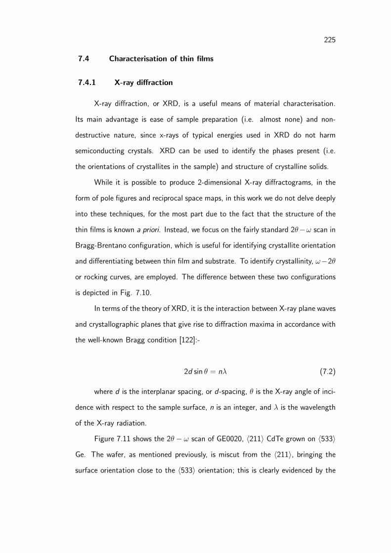
225
7.4 Characterisation of thin films
7.4.1 X-ray diffraction
X-ray diffraction, or XRD, is a useful means of material characterisation.
Its main advantage is ease of sample preparation (i.e. almost none) and non-
destructive nature, since x-rays of typical energies used in XRD do not harm
semiconducting crystals. XRD can be used to identify the phases present (i.e.
the orientations of crystallites in the sample) and structure of crystalline solids.
While it is possible to produce 2-dimensional X-ray diffractograms, in the
form of pole figures and reciprocal space maps, in this work we do not delve deeply
into these techniques, for the most part due to the fact that the structure of the
thin films is known a priori. Instead, we focus on the fairly standard 2θ−ω scan in
Bragg-Brentano configuration, which is useful for identifying crystallite orientation
and differentiating between thin film and substrate. To identify crystallinity, ω−2θ
or rocking curves, are employed. The difference between these two configurations
is depicted in Fig. 7.10.
In terms of the theory of XRD, it is the interaction between X-ray plane waves
and crystallographic planes that give rise to diffraction maxima in accordance with
the well-known Bragg condition [122]:-
2d sin θ = nλ (7.2)
where d is the interplanar spacing, or d -spacing, θ is the X-ray angle of inci-
dence with respect to the sample surface, n is an integer, and λ is the wavelength
of the X-ray radiation.
Figure 7.11 shows the 2θ − ω scan of GE0020, 〈211〉 CdTe grown on 〈533〉
Ge. The wafer, as mentioned previously, is miscut from the 〈211〉, bringing the
surface orientation close to the 〈533〉 orientation; this is clearly evidenced by the

226
X-ray source X-ray detector
Sample stage
Bragg-Brentano configuration
X-ray source X-ray detector
Sample stage
sample rocking
Rocking curve configuration
Figure 7.10: Configuration for X-ray diffraction
〈533〉 Ge reflection from Cu k−beta radiation, shown at approximately 107. The
〈533〉 for Cu k−alpha−1 radiation is rocked (i.e. ω−2θ scan) to determine quality
of the crystal; this is shown to have a FWHM of roughly 6 arc. sec. ω, indicative
of an extremely high quality crystal. The apparatus for this measurement involved
two 4-bounce crystals to ensure a very narrow X-ray beam and was performed at

227
0 20 40 60 80 100 120Degrees 2θ
Counts, a.u
CdTe <1 1 1>
CdTe <2 2 2>
CdTe <4 2 2>
CdTe <4 0 0>
Ge <4 0 0>C
dTe <4 2 2> - Cu k-β
Ge <5 3 3> - Cu k-β
GE0020 2θ/ω scan
35.200 35.300 35.400 35.500 35.600 35.700 35.800 35.900Degrees ω
FWHM = 389 arc seconds
CdTe <4 2 2>
63.23663.23863.24063.24263.24463.24663.248Degrees ω
FWHM = 6 arc seconds
Ge <5 3 3>
Figure 7.11: X-ray diffraction for GE0020, MBE grown 〈211〉CdTe on 〈533〉 Ge
the University of Illinois at Chicago. The rocking curve of the epilayer 〈422〉 is
also shown and gives a FWHM of 389 arc. sec. ω, indicating a fairly poor quality
epilayer. In this experiment, the growth temperature (250C ) was too low and far
from optimum; giving rise to an inhomogeneous epilayer. This temperature was
selected on the basis of published results, however subsequent experiments showed
that a higher growth temperature is beneficial to crystal quality. In addition, the
surface pretreatment, which consisted of exposure to Te flux, served to roughen
the surface. Finally, it is not altogether clear that 〈533〉 oriented germanium is
useful for growing 〈211〉 oriented CdTe under any circumstances; this was simply
the orientation provided by the manufacturer as an off the shelf product, saving
the expense of growing and sawing a custom ingot.
Figure 7.12 shows the 2θ − ω and ω − 2θ scans of SAPH001, CdTe 〈111〉
grown on 〈1012〉 sapphire using MBE at a substrate temperature of 305 C. The

228
0 20 40 60 80 100 120Degrees 2θ
Counts
, a.u
CdTe
<1 1
1>
Sapphire <
0 2
4>
- C
u k
-Beta
Sapphire <
0 1
2>
Sapphire <
0 2
4>
CdTe
<1 1
1>
- C
u k
-Beta
SAPH001 2θ/ω scan
11.800 11.820 11.840 11.860 11.880 11.900 11.920Degrees ω
FWHM = 72 arc seconds
DCRC of CdTe <1 1 1>
Figure 7.12: X-ray diffraction for SAPH001, MBE grown 〈111〉CdTe on 〈1012〉 Sapphire
2θ − ω scan clearly shows the presence of sapphire 〈012〉 (〈1012〉) and 〈024〉
(〈2024〉) reflections, which confirm substrate orientation as nominal 〈1012〉. The
difference in relative intensities may simply be explained by a slight miscut of
the substrate causing better fulfillment of the Bragg condition at 〈024〉. The
DCRC shown in the inset of Fig. 7.12 is performed using a Panalytical Empyrean
powder diffractometer with 4-bounce Ge 〈220〉 monochromator with 3-bounce
〈220〉 symmetrical analyzer for Cu. The sample is rocked about the CdTe 〈111〉.
The FWHM is roughly 72 arc. sec., which is an impressive result, given the film is
no thicker than 1 µm. For example, Badano et al. [125] report FHWM of roughly
360 arc seconds for comparable thickness films on Ge 〈211〉. This tends to indicate
a high quality crystal with comparatively few defects, and even better crystallinity
can be expected for thicker films [125].
On the other hand, Fig. 7.13, grown under almost identical conditions, but

229
0 20 40 60 80 100 120Degrees 2θ
Counts
, a.u
CdTe
<1 1
1>
CdTe
<1 1
1>
- C
u k
-Beta
SAPH002 2θ/ω scan
11.800 11.820 11.840 11.860 11.880 11.900 11.920Degrees ω
FWHM = 59 arc seconds
DCRC of CdTe <1 1 1>
Figure 7.13: X-ray diffraction for SAPH002, MBE grown 〈111〉CdTe on 〈1012〉 Sapphire
with a substrate temperature of 302 C, shows a much narrower full-width at half
maximum. This is partly due to a thicker film and partly due to more careful prepa-
rations during MBE growth and crystal nucleation. Finally, it could be argued that
the slight change in substrate temperature gave rise to more favourable outcomes.
Again, as an inset, the DCRC is plotted with a FWHM of roughly 59 arc. secs.,
a very high quality crystal indeed. Although difficult to see due to low X-ray yield
(in general, 2 bounce Ge 〈220〉 or 4-bounce Ge 〈440〉 monochromators/analyzers
are preferred for rocking curves, which reduce drastically x-ray counts), side-lobes
are clearly visible on the rocking curve.
Figure 7.14 depicts the X-ray diffraction of polycrystalline ZnTe on R-plane
sapphire. Since the films prepared by thermal evaporation are reasonably thin (≃
300 nm), it is not feasible to scan using the Bragg-Brentano configuration, or for
that matter, perform rocking curves. The reason being partially that ZnTe is itself

230
10 20 30 40 50 60 70 80 90Degrees 2θ
Co
un
ts,
a.u
Zn
Te <
1 1
1>
Zn
Te <
2 2
0>
Zn
Te <
3 1
1>
Zn
Te <
2 2
2>
Zn
Te <
4 2
0>
ZnTe / Sapphire 2θ/ω scan
12.30012.40012.50012.60012.70012.80012.90013.000Degrees ω
FWHM = 449 arc seconds
ZnTe <1 1 1>
Figure 7.14: X-ray diffraction for ZnTe thermally evaporated on〈1012〉 Sapphire
not sufficiently dense to stop a significant proportion of X-rays at that thickness,
so reflections from the substrate itself will dominate. Additionally, in this case, the
d -spacing of both R-plane sapphire and ZnTe is very similar, further necessitating
suppression of substrate reflections. However, it is still possible to analyze these
very thin films using glancing angle scans. In such a scan, the source is positioned
with a fixed angle ω which is very small, i.e. < 4 degrees. Then the angle the
detector makes with the substrate (i.e. θ) is varied as in a normal 2θ−ω scan, and
diffraction maxima are still observed at corresponding values of 2θ (the detector
angle) as if the scan were indeed in Bragg-Brentano configuration.
7.4.2 Reflection high-energy electron diffraction (RHEED)
Reflection high-energy electron diffraction (RHEED) is related to transmis-
sion electron diffraction and indeed low-energy electron diffraction (LEED). It

231
10 20 30 40 50 60 70Degrees 2θ
Counts, a.u
ZnTe <1 1 1>
ZnTe <2 2 0>
ZnTe <3 1 1>
ZnTe <2 2 2>
Ge <3 1 1>
ZnTe <4 2 0>
ZnTe / Ge 2θ/ω scan
12.30012.40012.50012.60012.70012.80012.90013.000Degrees ω
FWHM = 471 arc seconds
ZnTe <1 1 1>
Figure 7.15: X-ray diffraction for ZnTe thermally evaporated on〈100〉 Germanium
(a) CdTe on germanium, After 4 minutes
(b) CdTe on germanium, After 1 hour
Figure 7.16: RHEED patterns and XRD of CdTe grown on Ge

232
differs mainly in the use of very low angles of incidence, i.e. < 10, and very
high energies, i.e. > 10keV. This allows the condition of the surface, rather than
the bulk, to be imaged, which gives clues to the surface reconstruction, or said
otherwise, the arrangement of atoms on the surface, which may be different to
that of the bulk.
RHEED is particularly suited to MBE growth chambers since it can be used
to accurately image the surface of a growing crystal, i.e. in situ. This is due
to the ultra-high vacuum of the MBE growth chamber which facilitates in-situ
characterisation techniques.
Figure 7.16 depicts the RHEED patterns during growth for CdTe grown on
Ge at various stages of the growth. The RHEED pattern shows a series of dots
indicating reasonable quality nucleation and 2D growth. The dots then become
streaks as growth continues and the surface becomes smooth [25].
7.4.3 Nomarski contrast microscopy

233
50um
Figure 7.17: Normarski contrast micrograph of SAPH001
Nomarski contrast microscopy shows a comparatively featureless growth for
SAPH001, the CdTe grown on R-plane sapphire. The sample shows no obvious
defects but a corrugated surface with small hillocks of around 1 micron size. These
indicate a reasonable quality film.
7.4.4 Optical constants from transmission measurements
Since sapphire is 80 - 90% transparent in the short wave infrared (SWIR), UV
(ultra violet) and visible ranges, spectroscopic transmission measurements are pos-
sible to determine optical properties, film thickness, and to examine the absorption
tail around the band edge as a means to qualitatively assess the crystallinity.
The transmission data show a high quality CdTe 1 micron thick film on
sapphire with sharp cut-off indicating high quality material. The measurements
do not agree well with the model; the measured sample has a higher energy gap
(roughly 810 nm or 1.53 eV as opposed to 820 nm or 1.51 eV). This wider energy

234
gap may be due to the lattice constant not being exactly as assumed by the
model data due to the heteroepitaxy, i.e. a lattice strain effect. The compressively
strained layer may warp the energy bands producing the wider optical band gap.
It seems that additionally the optical properties differ between the model and the
measured thin film.
The 300 nm ZnTe film on sapphire however shows poor optical properties.
This is partially due to the the film thickness, but mostly due to the poor crys-
tallinity of the film. Again the optical properties differ between the model and the
measured data.

235
200 400 600 800 1000 1200 1400 1600 1800wavelength, nm
intensity, a.u
Optical transmission of CdTe ⟨111
⟩ on sapphire (SAPH002)
ModelMeas.
200 400 600 800 1000 1200 1400 1600 1800wavelength, nm
intensity, a.u
Optical transmission of polycrystalline ZnTe ⟨111
⟩ on sapphire
Figure 7.18: Optical transmission measurements of CdTe andZnTe thin films on sapphire
236
7.5 Electronic properties of the CdTe/Ge interface
7.5.1 Overview
Electronic properties of the CdTe/Ge heterointerface are not particularly
well known, most likely due to lack of interest in these materials, or disfavourable
material properties as discussed above. Nevertheless, since it has been shown
that it is indeed possible to grow material of sufficient quality for characterisation
purposes, we present here a process for the fabrication and characterisation of a
CdTe/Ge heterojunction.
7.5.2 Fabrication Process
CdTe material grown on Ge by molecular beam epitaxy (as described in
Section 7.3.3) was first doped using a copper spin-on dopant product (Cu950 from
Filmtronics, [Butler, PA, USA]) by spinning the silica based film onto a ≃ 1cm
× 1cm square sample which had been cleaned for 15s in a solution of Br/MeOH,
with care taken not to expose the sample to water (MeOH/isopropanol rinse and
dry). The Cu acceptor was diffused at 300 degrees for 1 hour to ensure uniform
diffusion within the CdTe epilayer (Cu diffusivity in Ge is comparatively low and the
solubility is below the substrate n-doping level, so diffusion of Cu acceptor ions into
the substrate may be neglected [126]). This has the effect of converting the CdTe
epilayer to p-type, whereas the n-type germanium substrate (donor concentration
≃ 1×1014cm−3) remains n-type. The reason for the low temperature is to prevent
Cd and Ge from alloying at the surface and, most importantly, to prevent surface
roughening of the CdTe due to Cd outdiffusion, which can occur at elevated
temperatures, especially around cracks and defects in the silica dopant film.
Subsequently, the dopant film is removed in dilute (≤ 10%) HF solution,
which does not affect the CdTe surface, at least if etching time is kept to a

237
minimum (e.g. 10-20s). The device region, e.g. Mesa, is then defined using
photolithograpy. Since the CdTe epilayer was in these cases quite thick (roughly
6 µm) this requires a fairly long etching time in 1% Br in HBr, which has an etch
rate of roughly 1 micron per minute at room temperature. Hence, to fully etch the
sample at least seven minutes etching time is required to ensure the all unwanted
material is fully removed, which requires fairly thick, robust photoresists. Of the
three positive photoresists, AZ4562, the thickest resist, was found to give best
results. Since etch rates vary as etchant is consumed, visual inspection using a
microscope was used to confirm successful termination of the etch process.
Contact Deposition
Photolithography Contact metal (Cr/Au) deposition Liftoff
Mesa Etch
Photolithography
Epilayer Doping
Spin-on Cu SOD
Mesa etch in 1% Br/HBr Photoresist strip
Diffuse on Hot Plate SOD film strip
Figure 7.19: CdTe/Ge heterojunction fabrication process
Finally, contacts could be made to the CdTe/Ge device using antimony

238
Au contacts
Cu doped
CdTe epilayer MESA
Ge wafer
Figure 7.20: Optical micrograph of CdTe / Ge heterojunctiondevice at 5x magnification
doped gold to form Ohmic contacts to both CdTe and Ge device layers. Although
thermally evaporated 1% Sb doped Au wire has traditionally been the preferred Ge
contact material, it was found that much comparable performance can be achieved
by first evaporating a thin layer of Cr to improve adhesion and prevent peeling (≃
5 nm), followed by a thin layer (5 - 20 nm) of Sb, and then evaporating a thicker
layer of Au (50 - 100 nm) which is subsequently annealed and hence alloyed.
Since alloying takes place at relatively high temperatures (400 - 500 C.) this
is not entirely practical with CdTe devices. Hence, these devices (GE020), were
processed without antimony, that is, using a pure Cr / Au contact, which was then
annealed for 30 minutes at 200 C on a hotplate to improve contact characteristics.
The contacts were patterned using lift-off patterning with a negative resist
(AZ2035) with release in warm acetone and ultrasonic bathing. The full device
fabrication process is tabulated in Fig. 7.19, with an optical micrograph of the
completed devices in Fig. 7.20.
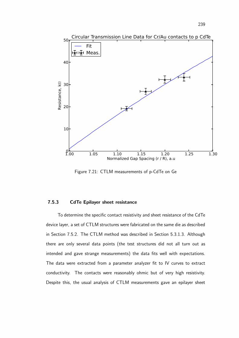
239
1.00 1.05 1.10 1.15 1.20 1.25 1.30Normalized Gap Spacing (r / R), a.u
0
10
20
30
40
50
Resistance, kΩ
Circular Transmission Line Data for Cr/Au contacts to p CdTe
FitMeas.
Figure 7.21: CTLM measurements of p-CdTe on Ge
7.5.3 CdTe Epilayer sheet resistance
To determine the specific contact resistivity and sheet resistance of the CdTe
device layer, a set of CTLM structures were fabricated on the same die as described
in Section 7.5.2. The CTLM method was described in Section 5.3.1.3. Although
there are only several data points (the test structures did not all turn out as
intended and gave strange measurements) the data fits well with expectations.
The data were extracted from a parameter analyzer fit to IV curves to extract
conductivity. The contacts were reasonably ohmic but of very high resistivity.
Despite this, the usual analysis of CTLM measurements gave an epilayer sheet

240
resistance 1 MΩ/ and a resistivity of 600 Ω · cm. The CTLM data is depicted
in Fig. 7.21.
7.5.4 CdTe / Ge heterojunction current-voltage characteristics
−1.0 −0.5 0.0 0.5 1.0Corrected bias, Volts - I ·RS , V
10-5
10-4
10-3
10-2
10-1
100
101
Curr
ent,
mA
IV Characteristics of CdTe / Ge rectifying heterojunction
I=Is ·(exp(
V−I ·Rs
1.6 ·kT )−1)
I=Is ·(exp(
V−I ·Rs
1.6 ·kT )−1)+ V
Rp
Meas.
Figure 7.22: CdTe / Ge heterojunction electronic properties
The current-voltage characteristics of the heterojunction were measured us-
ing a HP-4156 parameter analyzer using a set of adjustable gold probes between
±1 Volt. The results are plotted in Fig. 7.22. The device clearly displays rectifying
characteristics, but has a high series resistance of 10 kΩ. This series resistance
is due to the high resistivity on both sides of the junction. As we have seen, the
resistivity of the CdTe was approximately 600 Ω · cm, the resistivity of the Ge was
approximately 40 Ω · cm. From these resistivities and knowledge of the dimen-

241
sions of the device, a figure of 10kΩ seems unattributable to the bulk alone, and
a significant proportion of the series resistance must be attributable to contact
resistance. This illustrates the difficulty making contacts to both low doped n-Ge
and p-CdTe.
The device also exhibits shunt resistance of the order of 1.25MΩ, indicating
a reasonable quality interface with minimal leakage through the junction. This
means that the quality of the crystal growth is reasonable, with few pin-hole like
defects and inhomogeneities at the interface. The ideality factor is roughly 1.65
showing a reasonable quality diode, again highlighting the comparative quality of
the crystal growth.
7.5.5 CdTe/Ge heterojunction capacitance-voltage profiling
The capacitance of the heterojunction is given by the following relation [30]:-
Chj = A
√
q · ǫnǫp2
NaNd
(Naǫp + Ndǫn)(φbi − VA)(7.3)
A more useful quantity to consider is the inverse square of the capacitance,
since this transforms the complicated relation in Eqn. 7.3 into a simple linear
relationship.
1
C 2hj
=1
A2
2
q · ǫnǫp(Naǫp + Ndǫn)(φbi − VA)
NaNd
(7.4)
By inspection of Eqn. 7.4, it is evident that the x-intercept is equal to the
built in potential of the device. Furthermore, it is possible to determine the doping
profile as a function of depth in an unknown region of the device from the slope
of the 1C2hj
versus VA plot.

242
d
dV
(
1
C 2hj
)
= − 1
A2
2
q · ǫnǫp(Naǫp + Ndǫn)
NaNd
(7.5)
If the doping in one region of the Pn heterojunction is significantly higher
than in the other region, it is possible to solve Eqn. 7.5 analytically. In other cases,
graphical methods can be employed to determine the carrier concentration from
the transcendental equation. Since in this case the doping concentrations on both
sides of the heterointerface are comparable, this technique must be employed.
The capacitance-voltage profiling of the CdTe/Ge heterojunction is shown
in Fig. 7.23. Doping densities some distance from the junction are extracted
using the above techniques. The doping density for the germanium substrate is
computed from wafer resistivity (40 Ω · cm ≃ 1e14 cm−3). The values of the
dielectric constants for CdTe and Ge are taken to be 10.4 and 16 ǫ0 respectively
[2]. The built in potential is extracted by extrapolation of the 1C2hj
versus VA plot,
and is around 1.42V. This built in potential has components attributable to the
doping densities either side of the interface and the band offsets themselves, as
illustrated by equation Eqn. 2.46. If one band offset were known, the other
could be computed from this equation. The doping concentration extracted is
the acceptor concentration in the p-type CdTe and is fairly constant. From the
literature [127] we would expect a Gaussian profile of Cu acceptor ions at the
surface of the CdTe (a distance 6 µm from the junction as indicated in Fig. 7.23).
We do not see such a feature. This could be attributable to the limited accuracy
of the CV profiling at such a distance from the junction. The doping density
extracted, however, may not be completely due to the introduction of copper ion
but may be due to a native defect that arises during the diffusion process, which
serves to anneal and activate the sample in air, a common step in CdTe solar cell
processing.

243
−10 −8 −6 −4 −2 0 2Bias, V
0.00
0.01
0.02
0.03
0.04
0.05
0.06
0.071
/ C
apaci
tance
square
d, 1/pF2
1/C2 −V Plot of CdTe/Ge heterojunction
0
5
10
15
20
25
30
35
40
Capaci
tance
, pF
Built in potential = 1.42±0.1 V
−6 −5 −4 −3 −2 −1 0Distance from junction, µm
1013
1014
1015
Dopin
g c
once
ntr
ati
on, cm
−3
Emitter doping profile of CdTe/Ge heterojunction
Figure 7.23: CdTe / Ge heterojunction capacitance profiling
7.6 Summary and conclusions
In this chapter we computed the true orientation of substrates used in this
work using the stereographic projection. We noted the misorientation of wafers

244
can lead to a dramatic change in wafer orientation, for instance nominally <2 1
1> wafers were in fact oriented <5 3 3>. This is important to take notice of,
particularly when performing XRD on these samples. This also effects the growth
orientation for crystals grown on such wafers.
ZnTe thin films were prepared using a simple thermal evaporation method,
based on preparing stoichiometric ZnTe from Zn and Te and mixing in a crucible
to form a stoichiometric source. The ZnTe was deposited at temperatures ranging
from 200 to 400C . Optically transparent and reasonably uniform films were
deposited within this temperature range.
Molecular Beam Epitaxy was employed to deposit high quality CdTe films
on both germanium and sapphire substrates. MBE is the growth technology of
choice for high quality semiconducting films with good control over interfaces
and material composition. This growth technology yielded high quality layers as
compared to thermal evaporation. The success of the sapphire grown samples
illustrates that MBE is a viable technology for experimentation with mechanically
stacked multijunction CdTe solar cells utilising sapphire substrates.
Optical contrast microscopy allowed the surface morphology of the as-deposited
epilayer to be examined. The surface morphology was smooth and did not feature
any noticeable defects. The surface was slightly corrugated with small hillocks of
1 micron in size. The overall appearance was seen to indicate a reasonable quality
film.
In situ RHEED was used during growth to characterise the film in situ and
showed high quality nucleation followed by a transition to smooth morphology with
a streaky appearance of the RHEED pattern. RHEED was also used during initial
preparations to determine the growth temperature by adjusting the temperature
prior to nucleation iteratively according to the RHEED pattern. RHEED is a
useful characterisation tool and one of the many advantages of ultra-high vacuum

245
technologies such as MBE.
Optical transmission measurements showed high quality films with good op-
tical transparency. The films did not match up with the models particularly well
with differing optical bandgaps and optical properties. Nonetheless, the films
themselves showed good properties highlighting the quality of the material.
X-ray diffraction was used to investigate the crystallinity of samples of CdTe
and ZnTe prepared on Ge and Sapphire. The samples prepared on sapphire had the
best crystallinity as shown by double crystal rocking curves (DCRC) full width at
half maximum (FWHM) as low as 59 arc seconds about the < 1 1 1 > diffraction
plane, indicating a very high quality crystal. The samples prepared on < 5 3 3 >
Ge was less crystalline owing to suboptimal growth conditions. The ZnTe samples
were polycrystalline due to the simpler, lower quality deposition technology.
A CdTe/Ge heterojunction was fabricated using copper spin-on dopants to
dope the CdTe region p-type with Cu acceptors. Current-voltage (IV) and capac-
itance voltage (CV) measurements were made of the heterojunction diode. The
diode showed rectifying characteristics, a series resistance of approximately 10kΩ,
a shunt resistance of 1.25MΩ, and an ideality factor of 1.65. This indicated a
reasonable quality diode had been formed. The CV profiling showed a built-in
potential of 1.42V and the extracted doping concentration indicated the doping
profile was fairly uniform throughout the epilayer. This may be attributable to
doping due to a native defect in the CdTe which was activated during the diffusion
process.
The CdTe/Ge heterojunction shows that the electronic properties of the
CdTe/Ge interface are suitable to create a heterojunction device such as a tandem
solar cell, since the device showed good characteristics over a certain voltage
range and obeyed theory well enough to admit a simple curve fit. The fitted
curve had ideality factor 1.65, showing the presence of defects in the device most

246
likely due to the lattice mismatch, the skewed orientation of the substrate and the
suboptimal growth conditions. Future investigations of CdTe/Ge heterojunctions
could include deep-level transient spectroscopy (DLTS) to determine the energy
levels of the defects at the CdTe/Ge interface. This technique can yield a wealth
of information about the electronic properties of CdTe and Ge which can feed back
into device models. Knowledge of the trap levels in the interface could help design
an optimised tunneling/recombination junction and improve solar cell efficiency.
In summary, it was shown that it is possible to grow high quality II-VI films
on sapphire, an optically transparent, mechanically hard, and insulating substrate.
This shows that mechanically stacked multijunction solar cells featuring high qual-
ity II-VI thin films grown on sapphire are physically realisable and should be consid-
ered. Future work should include in situ doping of the II-VI films during epitaxial
growth to realise complete tandem structures on sapphire. These structures can
then easily be combined with the germanium pn-junction diode and solar cell pro-
cess developed in this work and presented in Chapter 6. It was also shown that the
electronic properties of the CdTe/Ge heterojunction were favourable and a device
was fabricated to show this. This tends to indicate that a monolithic device should
be possible, however further work is needed to devise processes for heavily doping
cadmium telluride, since the doping density achieved with copper spin on doping
was not particularly high.

Chapter 8
Conclusions
8.1 Summary
Throughout this work we have been concerned with demonstrating the feasi-
bility of germanium as a bottom cell for monolithic or mechanically stacked tandem
solar cells with cadmium telluride. We have found that monolithic growth of the
materials is possible but troublesome and plagued with difficulties, particularly re-
lating to high temperature processing. Since Ge and CdTe form a eutectic alloy
at around 319 C , there is a restriction on the temperatures that can be used
on CdTe devices deposited on Ge. Also, the lattice mismatch makes it difficult to
grow high quality CdTe epilayers on top of Ge, even using a high-cost, low deposi-
tion rate technology like MBE. Nevertheless, a CdTe/Ge heterojunction device was
created that allowed electronic properties of the heterostructure to be explored.
This device was fabricated using MBE grown CdTe on Ge grown at the University
of Illinois at Chicago, and processed at the UWA clean room (A. G. Nassibian
Nanofabrication Facility). The device was a P/n heterojunction and exhibited
good rectifying characteristics, with ideality factor of 1.65 indicating reasonable
quality material and a shunt resistance of 1.25 MΩ suggesting very few shunt like
defects at the material interface.
Work was undertaken to develop low cost technologies for device active re-
gion formation. The techniques investigated were direct spin-on doping, proximity
248
doping, and sandwich stacked diffusion. Direct spin-on doping is seen to give the
best profile for phosphorus doped devices in terms of abruptness, however, direct
spin on doping was to be avoided due to issues with inhomogeneities and defects
causing poor yield. Proximity doping was shown to give favourable results but
lacked the surface concentration for P and Sb necessary for degenerate doping.
Proximity doping was shown to work quite well for Ga as well, and degenerate
doping could be achieved. Finally, sandwich stacked diffusion, the novelty intro-
duced in this thesis, was used to degenerately dope Ge with Ga acceptors. These
low-cost techniques are all amenable to mass manufacture and adaptable to the
mass manufacturing environment. These techniques could one day be used to
form the Ge junction part of a CdTe/Ge tandem solar cell.
To demonstrate the viability of the low cost doping technologies, Ge diodes
were fabricated using Ge single crystal wafers from Sylarus inc. [St. George,
Utah, USA] and University Wafer [Boston, MA, USA]. These were seen to be high
quality diodes with ideality factors close to 1. These devices did suffer from Zener
breakdown in reverse bias. However, on the lower doped substrate, the reverse
breakdown occurred at -25V which is acceptable reverse breakdown performance.
These devices illustrated the use of the low cost doping techniques.
Passivation technologies were investigated and it was found that a pre-
treatment using ammonia followed by a-Si:H/SiNx passivation layer deposition
gave the most favourable surface recombination velocities, with a surface recom-
bination velocity as low as 21 cm/s reported in this work. This was as compared
with unpassivated but chemically treated control samples as well as a variety of
other passivation techniques, including hydrogen pretreatement and SiO2 passiva-
tion layers. These passivation technologies are again low cost and amenable to
mass-manufacture.
Antireflection coatings to Ge were optimised and a final design of a-Si:H,

249
SiNx and MgF2 of thicknesses 10-80 nm, 50-60 nm, and 80-90 nm, respectively,
were found to minimise reflectivity. Specifically, for thicknesses 76nm (a-Si:H),
58nm (SiNx) and 89nm (MgF2) the reflectivity was reduced to 6.47%. However,
thicker a-Si:H implies more absorption and hence less transmission to the underly-
ing Ge layer. Hence it is favourable to trade off reflectivity for transmissivity and
thus incorporate a thinner amorphous silicon layer.
Contacts were fabricated and optimised to germanium. It was found that
Ni had the best specific contact resistivity but was hard to measure with the test
structures in question since the resistances involved were so low the measurements
had impaired accuracy. A specific contact resistivity of 1.26 ×10⁻⁷ Ω · cm2 is
reported. Other metals investigated included Al, Cr/Au and Ti. With the exception
of Al, all metals made good quality ohmic contacts to the germanium.
Ge solar cells were fabricated, with a peak efficiency of 5.4%. Although this
is not world changing in and of itself, it nevertheless demonstrates the technology.
These cells were fabricated from single crystal germanium by using the techniques
developed in this work: that is, diffusion by low cost proximity doping technique,
passivation and anti-reflection coating, and contacts. Hence it is fair to say that
the solar cell symbolises the culmination of all the thesis’ work in one single device.
The device was stable 8-9 months after initial testing which proved the potential
efficacy of the passivation layer as an environmental passivant. However, a lack of
environmental testing means the conclusions which may be drawn are limited.
Single crystal CdTe was grown of very good quality on R-plane sapphire.
The best X-ray DCRC FWHM was 59 arc seconds, indicating very high quality
material. Since this is a viable option, it may be possible to create mechanically
stacked tandem solar cells with top cell featuring CdTe grown on sapphire. This
could be a possible future research direction.

250
8.2 Research outcomes
The key research aims of this work were to reduce surface recombination in
Ge standalone solar cells with adequate surface passivation, to make low resistivity
contacts to germanium, and form device regions in a low cost manner without
any unwanted contamination which may impair device efficiency. These aims
were addressed sufficiently by the research in this work. Further research aims
included to investigate the feasibility of combining CdTe and Ge together to form
an electronic device and determine the electronic properties of the heterostructure.
This was also addressed and a viable heterojunction was demonstrated.
The following can be concluded about the combination of CdTe with Ge:-
• MBE growth yields good results, but heteroeptiaxy is difficult due to lattice
mismatch
• The optimum growth MBE temperature lies somewhere between 300 and
305C , and the optimum fluxes are beam equivalent pressure (BEP) 1.1e-
6 Torr for CdTe, and 1.5e-6 Torr for Te.
• Care must be taken to always keep the temperature of the sample below
the eutectic point (319 C ) to prevent alloying of CdTe and Ge. This is
particularly necessary if annealing in the presence of Cd vapour.
Provided that low temperature processing is used, monolithic CdTe and Ge
devices can be adequately fabricated with good electronic properties. If elevated
processing temperatures are required, a mechanically stacked tandem should be
pursued, and for this case, sapphire can be used as an optically transparent sub-
strate.

251
8.3 Future work
Due to time and budget constraints, sandwich-stacked diffusion was only
investigated for Ga spin-on dopants and only with diffusion followed by drive-in.
It would be highly recommended to research all dopants investigated in this work
using this technique to determine its applicability to a wide range of dopant sources.
Furthermore, models for dopant profiles should be compiled so that devices can
be designed. It would be interesting to see if higher surface concentrations can be
achieved with sandwich-stacked diffusion for the high vapour pressure phosphorus
dopant sources. If so, this will overcome some of the limitations of phosphorus
proximity doping which cannot achieve a high surface concentration due to the
high vapour pressure and volatility of phosphorus.
Process models need to be focussed on to improve the prospects of realising
a tunnel-diode. In particular, co-doping with phosphorus and gallium needs to
be investigated to determine the effects one dopant has on the diffusivity of the
other. Such a study should make extensive use of secondary ion mass spectrometry
(SIMS) depth profiles to adequately ascertain the secondary effects of codoping.
These models then need to be utilised to design a tunnel diode, which can then be
used to realise the structure introduced in Chapter 3, which consisted of an all-Ge
tunnel/recombination junction.
Work needs to be undertaken to improve the efficiency of the standalone
germanium solar cells. Their efficiency was hampered by two main factors: poor
quality VGF wafers from JMP technology Sarl, which contained a great many
defects and dislocations, and poor fill factor attributed to high series resistance due
to insufficiently thick front contacts. A technology needs to be developed for thick
plating of contacts to micron scale thickness. One possible technique would be
a simple nanoparticle paste which is spread on the contact material and annealed

252
to form a thick contact. Waste material should not adhere to the passivation
layer and should instead “ball up” or migrate to the contacts. An example nano-
particle paste would be simple Sn/Pb solder paste. Other nanoparticle pastes
might be suitable. Another possible technology could be electroplating. Thick
layers of contact material could be deposited by passing a current through the
device itself in a chemical bath. Finally, inkjet printing with nanoparticle inks is
a novel technology that has only recently entered the research arena. This could
be used combined with annealing with a nanoparticle solution of, for example, Ni,
to make thick low resistivity contacts to the Ge. These techniques should lower
series resistance and improve fill factor.
Open circuit voltage can be improved in the solar cells by using slightly
more heavily doped wafers. The wafers from JMP Technology Sarl were nominally
1e17 cm−3 doped. By raising the substrate doping to 5e17 or 1e18 cm−3 a few
tens of millivolts open circuit voltage can be gained. In addition, open circuit
voltage is limited by shunt resistance. The device presented in chapter 6 had a
suboptimal shunt resistance which can be attributed to defects during the doping
process which are more prominent in this device due to its larger area. This means
the proximity doping technique is still affected by defects and inhomogeneities
present in the spin-on dopant matrix. Or alternatively, the shunt resistance may
be attributable to lateral defects due to the dislocations on the wafer itself as
evidenced by SEM on a similarly fabricated diode. Again, due to large area, the
perimeter is considerable and will contain a great many of these defects, some
located within the junction. These may be the cause of the shunt resistance, in
which case simply changing wafer manufacturers should solve this problem.
It was seen that the optical transparency of the a-Si:H films was not partic-
ularly good. There are two reasons for this, one is that the optical band gap of
the film lies within the visible range, and hence absorbs energy (a-Si:H has a rea-

253
sonably high absorption coefficient, hence its use in thin film solar cells); the other
is the presence of excess hydrogen. It should be possible to anneal out some of
the excess hydrogen without adversely affecting the device. Of critical importance
is that the passivating interactions at the surface when prepared with ammonia
pretreatment are not interfered with during the annealing process. For example, it
is thought that nitrogen plays a role in terminating the lattice and passivating Ge
dangling bonds. If so, the passivation should be relatively unaffected by thermal
treatment. If however hydrogen itself is responsible in part for the passivation of
the surface, then it is unlikely that the structure will be temperature-stable and
hence may degrade during the process. This warrants further investigation.
Future work should encompass doping studies of CdTe. Since spin-on Cu
solution worked quite well to form a simple heterojunction diode, this avenue may
be followed. To increase doping density, higher temperatures need to be consid-
ered. This means the experiments need to take place in saturated Cd environment
with Cd overpressure supplied from a solid charge to prevent Cd out-diffusion and
damage to the epilayer structure. This necessitates annealing in sealed ampoules.
This technique would be limited to sapphire substrates since Ge will dissolve in
the Cd environment forming a eutectic alloy. A much better alternative would be
to develop in situ doping in the MBE system itself. As for choice of dopants, it
would be difficult indeed to find suitable materials since in situ doping of CdTe is
quite difficult. It may be possible to use iodine or indium as donors, and antimony
or arsenic as acceptors but would require a great amount of work to perfect this
technology.
Growth of CdTe on Ge needs to be improved to reduce the full width at half
maximum of double crystal X-ray rocking curves. Perhaps a better orientation of
wafer should be chosen since growth on <5 3 3> germanium was not particularly
successful. A better orientation is <1 0 0> but if miscut for epitaxy then X-ray

254
peaks can be difficult to find.
8.4 Final Conclusions
This thesis has demonstrated a low cost fabrication process for germanium
optoelectronic devices including solar cells, that features optimised passivation and
contacting technologies. Low cost techniques for device active region formation
were demonstrated. The process as a whole was amenable to mass manufacture.
The devices were stable over time indicating that the passivation was adequate.
These key elements were satisfied in the context of developing the technology
for monolithic and mechanically stacked tandem solar cells. It was shown that
the doping densities demanded in the modelling and design of the tandem solar
cells could be achieved using the low cost technologies developed in this work, at
least in the case of Ge. Heavy doping of CdTe could not be demonstrated, but
moderate doping was achieved using a Cu spin-on dopant source. A solar cell
of moderate efficiency was demonstrated using the diode process. This solar cell
could be improved by many of the techniques discussed in the previous section.
Having satisfied the main research aims, this thesis has been moderately
successful. It is perhaps lamentable that a full tandem solar cell could not be
fabricated, however the amount of work involved in fabricating such a device and
developing from scratch the technology to do so is well outside the realm of a single
PhD thesis. Several recommendations for future work in the previous section tackle
the work involved and break it down into smaller pieces.
Since the author chose to carry out this study at a research group with a
background in infrared detectors, it is not surprising that the main outcome has
been a high-quality process for photodiodes as opposed to large area solar modules.
This is simply a question of research know-how within a research group. Since this
was the first solar project that this group has ever undertaken, the outcome of

255
working solar cells and high quality diodes can be seen as a major success. Should
the research into solar cells at the Microelectronics Research Group continue, there
should be no reason why efficiencies cannot match those of world leading research
groups, as intellectual property is developed over time.

Bibliography
[1] United States Geological Survey report. Min-erals yearbook: Selenium and tellurium.www.minerals.usgs.gov/minerals/pubs/commodity/selenium/myb1-2013-selen.pdf, 2013.
[2] Sadao Adachi. Properties of Group IV, III-V, and II-VI Semiconductors.Wiley, Jun 2005.
[3] William Shockley and Hans J. Queisser. Detailed Balance Limit of Efficiencyof p-n Junction Solar Cells. Journal of Applied Physics, 32(3):510, 1961.
[4] A.D. Vos. Detailed balance limit of the efficiency of tandem solar cells.Journal of Physics D: Applied Physics, 13:839, 1980.
[5] K. Mitchell, A.L. Fahrenbruch, and R.H. Bube. Photovoltaic determina-tion of optical-absorption coefficient in CdTe. Journal of Applied Physics,48(2):829–830, 1977.
[6] Alan L. Fahrenbruch. II-VI photovoltaic heterojunctions for solar energyconversion. Applied Physics Letters, 25(10):605, 1974.
[7] K Durose. Materials aspects of CdTe/CdS solar cells. Journal of CrystalGrowth, 197(3):733–742, February 1999.
[8] Y.Y. Ma, A.L. Fahrenbruch, and R.H. Bube. Photovoltaic properties of n-CdS/p-CdTe heterojunctions prepared by spray pyrolysis. Applied PhysicsLetters, 30(December 1976):423, 1977.
[9] Muren Chu, Alan L. Fahrenbruch, Richard H. Bube, and James F. Gibbons.Photovoltaic properties of CdTe p-n junctions produced by ion implantation.Journal of Applied Physics, 49(1):322, 1978.
[10] J. G. Werthen, a. L. Fahrenbruch, R. H. Bube, and J. C. Zesch. Surfacepreparation effects on efficient indium-tin-oxide-CdTe and CdS-CdTe het-erojunction solar cells. Journal of Applied Physics, 54(5):2750, 1983.

257
[11] H Matsumoto, K Kuribayashi, H Uda, Y Komatsu, a Nakano, and S Ikegami.Screen-printed CdS/CdTe solar cell of 12.8% efficiency for an active area of0.78 cm2. Solar Cells, 11(4):367–373, May 1984.
[12] JM Woodcock, AK Turner, ME Ozsan, and JG Summers. Thin filmsolar cells based on electrodeposited CdTe. In Photovoltaic SpecialistsConference, 1991., Conference Record of the Twenty Second IEEE, pages842–847. IEEE, 1991.
[13] Armin G. Aberle. Thin-film solar cells. Thin Solid Films, 517(17):4706–4710,July 2009.
[14] J. Britt and C. Ferekides. Thin-film CdS/CdTe solar cell with 15.8% effi-ciency. Applied Physics Letters, 62(22):2851, 1993.
[15] X Wu, R G Dhere, D S Albin, T A Gessert, C Dehart, J C Keane, A Duda, T JCoutts, S Asher, D H Levi, H R Moutinho, Y Yan, T Moriarty, S Johnston,K Emery, and P Sheldon. High-Efficiency CTO / ZTO / CdS / CdTePolycrystalline Thin-Film Solar Cells. Renewable Energy, (October), 2001.
[16] M. Shao, a. Fischer, D. Grecu, U. Jayamaha, E. Bykov, G. Contreras-Puente,R. G. Bohn, and a. D. Compaan. Radio-frequency-magnetron-sputtered Cd-S/CdTe solar cells on soda-lime glass. Applied Physics Letters, 69(20):3045,1996.
[17] Akhlesh Gupta and Alvin D. Compaan. All-sputtered 14% CdSCdTe thin-film solar cell with ZnO:Al transparent conducting oxide. Applied PhysicsLetters, 85(4):684, 2004.
[18] Martin A Green, Keith Emery, Yoshihiro Hishikawa, Wilhelm Warta, andEwan D Dunlop. Solar cell efficiency tables ( Version 45 ). Progress inPhotovoltaics: Research and Applications, 23:1–9, 2015.
[19] R. Venkatasubramanian, M.L. Timmons, R.T. Pickett, T.S. Colpitts, J.a.Hancock, J.S. Hills, and J.a. Hutchby. High-temperature performance andradiation resistance of high-efficiency Ge and Si/sub 0.07/Ge/sub 0.93/solar cells on lightweight Ge substrates. The Conference Record of theTwenty-Second IEEE Photovoltaic Specialists Conference - 1991, pages 85–89, 1991.
[20] V.P. Khvostikov, O.a. Khostikov, E.V. Oliva, V.D. Rumyantsev, M.Z.Shvarts, T.S. Tabarov, and V.M. Andreev. Zinc-diffused InAsSbP/InAs andGe TPV cells. Conference Record of the Twenty-Ninth IEEE PhotovoltaicSpecialists Conference, 2002., pages 943–946.
[21] NE Posthuma and G Flamand. Development of stand-alone germanium solarcells for application in space using spin-on diffusants. 3rd World Conferenceon Energy Conversion, 2003, pages 777–780, 2003.
258
[22] Niels E. Posthuma, Johan van der Heide, Giovanni Flamand, and JozefPoortmans. Emitter Formation and Contact Realization by Diffusion forGermanium Photovoltaic Devices. IEEE Transactions on Electron Devices,54(5):1210–1215, May 2007.
[23] Nobuo Matsumura, Takefumi Ohshima, Junji Saraie, and Yutaka Yodogawa.Preparation of CdTe thin films on Ge substrates by molecular beam epitaxy.Journal of crystal growth, 71(2):361–370, 1985.
[24] J Zanatta. Heteroepitaxy of CdTe on Ge(2 1 1) substrates by molecularbeam epitaxy. Journal of Crystal Growth, 184-185(1-2):1297–1301, February1998.
[25] R. Sporken, S. Sivananthan, K. K. Mahavadi, G. Monfroy, M. Boukerche,and J. P. Faurie. Molecular beam epitaxial growth of CdTe and HgCdTe onSi(100). Applied Physics Letters, 55(18):1879, 1989.
[26] N E Posthuma, G Flamand, W Geens, and J Poortmans. Surface passivationfor germanium photovoltaic cells. Solar Energy Materials and Solar Cells,88(2005):37–45, 2005.
[27] J. van der Heide, N.E. Posthuma, G. Flamand, W. Geens, and J. Poort-mans. Cost-efficient thermophotovoltaic cells based on germanium sub-strates. Solar Energy Materials and Solar Cells, 93(10):1810–1816, October2009.
[28] Niels Posthuma. HIGHLY EFFICIENT THIN GERMANIUM BOTTOMCELLS FOR MECHANICALLY STACKED HOTOVOLTAIC DEVICES. PhDthesis, KATHOLIEKE UNIVERSITEIT LEUVEN, 2005.
[29] J. P. Zanatta, P. Ferret, G. Theret, a. Million, M. Wolny, J. P. Chamonal,and G. Destefanis. Heteroepitaxy of HgCdTe (211)B on Ge substratesby molecular beam epitaxy for infrared detectors. Journal of ElectronicMaterials, 27(6):542–545, June 1998.
[30] S. M. Sze. Physics of Semiconductor Devices. John Wiley and sons, Inc.,New York, 1981.
[31] M Archer. A review of analytic solutions for a model p-n junction cell underlow-injection conditions. Solar Energy Materials and Solar Cells, 40(2):133–176, April 1996.
[32] Adrian Kitai. Principles of Solar Cells, LEDs, and diodes: The role of thepn junction. Wiley, 2011.
[33] D Bouhafs. Design and simulation of antireflection coating systems for opto-electronic devices: Application to silicon solar cells. Solar Energy Materialsand Solar Cells, 52(1-2):79–93, March 1998.

259
[34] Filiz Karaomerliogliu. Optical Properties of Multilayer Antireflection CoatingSystems on a Ferroelectric Base. PhD thesis, Insitute of Natural and AppliedSciences, Department of Physics, University of Cukurova, 2008.
[35] G. E. Stillman Charles M. Wolfe, Nick Holonyak. Physical properties ofsemiconductors. Prentice Hall, 1989.
[36] S. Selberherr. Analysis and simulation of semiconductor devices. SpringerVerlag, 1984.
[37] C. Ringhofer and C. Schmeiser. An Approximate Newton Method for theSolution of the Basic Semiconductor Device Equations. SIAM Journal onNumerical Analysis, 26(3):507–516, 2011.
[38] R.E. Bank, D.J. Rose, and W. Fichtner. Numerical methods for semiconduc-tor device simulation. Electron Devices, IEEE Transactions on, 30(9):1031–1041, 1983.
[39] RE Bank. Global approximate Newton methods. Numerische Mathematik,295:279–295, 1981.
[40] Donald Neamen. Semiconductor Physics And Devices. McGraw-Hill Sci-ence/Engineering/Math, 3rd edition, August 2002.
[41] Synopsis inc. Sentaurus device user guide, 2008.
[42] M. Shur M. Levenshtein, S. Rumyantsev. Handbook series on SemiconductorParameters, Vol I. World Scientific, 1996.
[43] L.A. Padilha, A.A.R. Neves, C.L. Cesar, L.C. Barbosa, and C.H. Brito Cruz.Auger recombination process in CdTe quantum dots. In Frontiers in Optics,volume 3392, pages 13083–13083. Optical Society of America, 2004.
[44] M.K. Ieong, P.M. Solomon, SE Laux, H.S.P. Wong, and D. Chidambar-rao. Comparison of raised and Schottky source/drain MOSFETs using anovel tunneling contact model. In Electron Devices Meeting, 1998. IEDM’98Technical Digest., International, pages 733–736. IEEE, 1998.
[45] A Morales-Acevedo. Thin film CdS/CdTe solar cells: Research perspectives.Solar Energy, 80(6):675–681, June 2006.
[46] S. A. Ringel, A. W. Smith, M. H. MacDougal, and A. Rohatgi. The effectsof CdCl2 on the electronic properties of molecular-beam epitaxially grownCdTe/CdS heterojunction solar cells. Journal of Applied Physics, 70(2):881,1991.
[47] C. Ferekides and J. Britt. CdTe solar cells with efficiencies over 15%. SolarEnergy Materials and Solar Cells, 35:255–262, September 1994.

260
[48] T.L. Chu, S.S. Chu, J. Britt, C. Ferekides, C. Wang, C.Q. Wu, and H.S.Ullal. 14.6% Efficient Thin-Film Cadmium Telluride Heterojunction SolarCells. IEEE Electron Device Letters, 13(5):303–304, May 1992.
[49] R.H. Bube, a.L. Fahrenbruch, R. Sinclair, T.C. Anthony, C. Fortmann,W. Huber, T. Thorpe, and T. Yamashita. Cadmium telluride films andsolar cells. IEEE Transactions on Electron Devices, 31(5):528–538, May1984.
[50] D Goren. Single crystalline CdTe solar cells grown by MOCVD. Solar EnergyMaterials and Solar Cells, 44(4):341–356, December 1996.
[51] TL Chu, SS Chu, C. Ferekides, J. Britt, and CW Wu. Thin film CdTe homo-junctions by MOCVD [solar cells]. In Photovoltaic Specialists Conference,1990., Conference Record of the Twenty First IEEE, pages 777–781. IEEE,1990.
[52] Lei Huang, Yue Zhao, and Dong Cai. Homojunction and heterojunctionbased on CdTe polycrystalline thin films. Materials Letters, 63(24-25):2082–2084, October 2009.
[53] A Compaan, A Gupta, S Lee, S Wang, and J Drayton. High efficiency,magnetron sputtered CdS/CdTe solar cells. Solar Energy, 77(6):815–822,December 2004.
[54] Karl W. Boer. CdS enhances Voc and fill factor in CdS/CdTe and Cd-S/CuInSe2 solar cells. Journal of Applied Physics, 107(2):023701, 2010.
[55] R. R. King, D. C. Law, K. M. Edmondson, C. M. Fetzer, G. S. Kin-sey, H. Yoon, R. a. Sherif, and N. H. Karam. 40% efficient metamor-phic GaInPGaInAsGe multijunction solar cells. Applied Physics Letters,90(18):183516, 2007.
[56] V. P. Khvostikov, O. a. Khvostikova, P. Y. Gazaryan, S. V. Sorokina, N. S.Potapovich, a. V. Malevskaya, N. a. Kaluzhniy, M. Z. Shvarts, and V. M. An-dreev. Photovoltaic Cells Based on GaSb and Ge for Solar and Thermopho-tovoltaic Applications. Journal of Solar Energy Engineering, 129(3):291,2007.
[57] Chao-Yang Tsao, Patrick Campbell, Dengyuan Song, and Martin a. Green.Influence of hydrogen on structural and optical properties of low temperaturepolycrystalline Ge films deposited by RF magnetron sputtering. Journal ofCrystal Growth, 312(19):2647–2655, September 2010.
[58] DL Pulfrey, J Dell, and L Faraone. Performance predictions for mono-lithic, thin-film CdTe/Ge tandem solar cells. In Society of Photo-OpticalInstrumentation Engineers (SPIE) Conference Series, volume 7750, page 98,2010.

261
[59] AD Katnani and G. Margaritondo. Microscopic study of semiconductor het-erojunctions: Photoemission measurement of the valance-band discontinuityand of the potential barriers. Physical Review B, 28(4):1944, 1983.
[60] Timothy J. Coutts, J. Scott Ward, David L. Young, Keith a. Emery, Tim-othy a. Gessert, and Rommel Noufi. Critical issues in the design of poly-crystalline, thin-film tandem solar cells. Progress in Photovoltaics: Researchand Applications, 11(6):359–375, September 2003.
[61] J. Yang, a. Banerjee, and S. Guha. Triple-junction amorphous silicon alloysolar cell with 14.6% initial and 13.0% stable conversion efficiencies. AppliedPhysics Letters, 70(22):2975, 1997.
[62] M. Vukadinovi, F Smole, M. Topi, and J Furlan. Numerical modelling oftrap-assisted tunnelling mechanism in a-Si: H and [mu] c-Si n/p structuresand tandem solar cells. Solar energy materials and solar cells, 66(1-4):361–367, 2001.
[63] Avi Braun, Baruch Hirsch, Eugene a. Katz, Jeffrey M. Gordon, WolfgangGuter, and Andreas W. Bett. Localized irradiation effects on tunnel diodetransitions in multi-junction concentrator solar cells. Solar Energy Materialsand Solar Cells, 93(9):1692–1695, September 2009.
[64] M. Hermle, F. Granek, O. Schultz, and S. W. Glunz. Analyzing the ef-fects of front-surface fields on back-junction silicon solar cells using thecharge-collection probability and the reciprocity theorem. Journal of AppliedPhysics, 103(5):054507, 2008.
[65] L. Esaki. Discovery of The Tunnel Diode. IEEE Transactions on ElectronDevices, 23(7):644–647, 1976.
[66] R K Ahrenkiel, B M Keyes, D L Levi, and K Emery. Spatial uniformity solarcells of minority-carrier lifetime in polycrystalline CdTe. Applied PhysicsLetters, 64(May):2879–2881, 1994.
[67] R. Quay V. Palankovski. Analysis and simulation of Heterostructure Devices.Springer, 2004.
[68] J. Tousek, D. Kindl, J. Touskova, S. Dolhov, and a. Poruba. Diffusion lengthin CdTe by measurement of photovoltage spectra in CdS/CdTe solar cells.Journal of Applied Physics, 89(1):460, 2001.
[69] E.D.Palik. Handbook of Optical Constants of Solids. Academic, New York,1991.
[70] H Hwang. Fundamental studies of p-type doping of CdTe. Journal of CrystalGrowth, 161(1-4):73–81, April 1996.

262
[71] Chao-Yang Tsao, Jurgen W. Weber, Patrick Campbell, Gavin Conibeer,Dengyuan Song, and Martin a. Green. In situ low temperature growth ofpoly-crystalline germanium thin film on glass by RF magnetron sputtering.Solar Energy Materials and Solar Cells, 94(9):1501–1505, September 2010.
[72] H Watakabe, T Sameshima, H Kanno, and M Miyao. Electrical propertiesfor poly-Ge films fabricated by pulsed laser annealing. Thin Solid Films,508(1-2):315–317, June 2006.
[73] J Fritsche. Band energy diagram of CdTe thin film solar cells. Thin SolidFilms, 403-404:252–257, February 2002.
[74] Nguyen Nhu Toan. SPIN ON GLASS MATERIALS AND APPLICATIONSIN ADVANCED IC TECHNOLOGIES. PhD thesis, University of Twente,1999.
[75] W. Zagozdzon-Wosik, P. B. Grabiec, and G. Lux. Silicon doping from phos-phorus spin-on dopant sources in proximity rapid thermal diffusion. Journalof Applied Physics, 75(1):337, 1994.
[76] W. C. Dunlap. Diffusion of Impurities in Germanium. Physical Review,94(6):1531, 1954.
[77] Suresh Uppal, Arthur F. W. Willoughby, Janet M. Bonar, Alan G. R. Evans,Nick E. B. Cowern, Richard Morris, and Mark G. Dowsett. Diffusion ofion-implanted boron in germanium. Journal of Applied Physics, 90(8):4293,2001.
[78] I. Riihimaki, a. Virtanen, S. Rinta-Anttila, P. Pusa, J. Raisanen, and TheISOLDE Collaboration. Vacancy-impurity complexes and diffusion of Gaand Sn in intrinsic and p-doped germanium. Applied Physics Letters,91(9):091922, 2007.
[79] Z. H. Lu. Air-stable Cl-terminated Ge(111). Applied Physics Letters,68(4):520, 1996.
[80] Arun V Thathachary, K N Bhat, Navakanta Bhat, and M S Hegde. Fermilevel depinning at the germanium Schottky interface through sulfur passiva-tion. Applied Physics Letters, 96(152108):2010–2013, 2010.
[81] M Nolan, T Perova, R A Moore, and H S Gamble. Boron diffusion from aspin-on source during rapid thermal processing. Journal of Non-CrystallineSolids, 254:89–93, 1999.
[82] Doug Ruby, Sandia National Laboratories, and Douglas Ruby. SIMULTANE-OUS P AND B DIFFUSION , IN SITU SURFACE PASSIVATION , IMPU-RITY FILTERING AND GETTERING FOR SILICON SOLAR CELLS. 26thIEEE Photovoltaic Specialists Conference, (September), 1997.

263
[83] Ji Youn Lee and Soo Hong Lee. Boron Back Surface Field Using Spin-OnDopants by Rapid Thermal Processing. Energy, 44(6):1581–1586, 2004.
[84] W. van Roosbroek C. S. Fuller, H. C. Theurer. Properties of ThermallyProduced Acceptors in Germanium. Physical Review, 85(4):678–679, 1952.
[85] Dieter K. Schroder. Semiconductor Material and Device Characterization.Wiley-IEEE Press, 3rd edition, 2006.
[86] S. Brotzmann, H. Bracht, E. Simoen, E. E. Haller, J. S. Christensen, andP. Werner. Diffusion and defect reactions between donors, C, and vacanciesin Ge. I. Experimental results. Physical Review B, 77(23):235207, June2008.
[87] J. Crank. The Mathematics of Diffusion. Clarendon Press, Oxford, 1975.
[88] R. Kube, H. Bracht, a. Chroneos, M. Posselt, and B. Schmidt. Intrinsicand extrinsic diffusion of indium in germanium. Journal of Applied Physics,106(6):063534, 2009.
[89] E. Huger, U. Tietze, D. Lott, H. Bracht, D. Bougeard, E. E. Haller, andH. Schmidt. Self-diffusion in germanium isotope multilayers at low temper-atures. Applied Physics Letters, 93(16):162104, 2008.
[90] Sergej Brotzmann and Hartmut Bracht. Intrinsic and extrinsic diffusionof phosphorus, arsenic, and antimony in germanium. Journal of AppliedPhysics, 103, 03350(2008), 2008.
[91] Rong Chen and Stacey F. Bent. Highly Stable Monolayer Resists forAtomic Layer Deposition on Germanium and Silicon. Chemistry of Materials,18(16):3733–3741, August 2006.
[92] Chi On Chui, Hyoungsub Kim, David Chi, Baylor B Triplett, Paul C Mcintyre,and Krishna C Saraswat. A Sub-400C Germanium MOSFET Technologywith High-K Dielectric and Metal Gate. Electron Devices Meeting, 2002.IEDM ’02. International, (650):437–440, 2002.
[93] L. Surnev and M. Tikhov. Comparative study of hydrogen adsorption onGe(100) and Ge(111) surfaces. Surface Science 138 (1984) 40-50, 138:40–50, 1984.
[94] J. R. Weber, a. Janotti, P. Rinke, and C. G. Van de Walle. Dangling-bonddefects and hydrogen passivation in germanium. Applied Physics Letters,91(14):142101, 2007.
[95] Sandrine Rivillon, Yves J. Chabal, Fabrice Amy, and Antoine Kahn. Hydro-gen passivation of germanium (100) surface using wet chemical preparation.Applied Physics Letters, 87(25):253101, 2005.

264
[96] Pendar Ardalan, Evan R. Pickett, James S. Harris, Ann F. Marshall, andStacey F. Bent. Formation of an oxide-free GeTiO[sub 2] interface by atomiclayer deposition on brominated Ge. Applied Physics Letters, 92(25):252902,2008.
[97] S Cao, J-C Tang, and S-L Shen. Multiple-scattering and DV-X α analysesof a Cl-passivated Ge(111) surface. Journal Physics: Condensed Matter,15(2003):5261–5268, 2003.
[98] Wang H Jiang D S Jin R Q Huang Y Zhang S M Yang H Jahn U PloogK H Sun Q. Spatial distribution of deep level defects in crack-free AlGaNgrown on GaN with a high-temperature AlN interlayer. Journal of AppliedPhysics, 100(12), 2006.
[99] Louis M Nelen, Kathryn Fuller, and C Michael Greenlief. Adsorption anddecomposition of H2S on the Ge(100) / surface. Applied Surface Science,150:65–72, 1999.
[100] G. W. Anderson, M. C. Hanf, P. R. Norton, Z. H. Lu, and M. J. Graham.The S-passivation of Ge(100)-(11). Applied Physics Letters, 66(9):1123,1995.
[101] Yi Zhou, Wei Han, Yong Wang, Faxian Xiu, Jin Zou, R. K. Kawakami,and Kang. L. Wang. Investigating the origin of Fermi level pinning in GeSchottky junctions using epitaxially grown ultrathin MgO films. AppliedPhysics Letters, 96(10):102103, 2010.
[102] Qingheng Hua. Thin germanium nitride films grown by thermal reactionprocess. Journal of Applied Physics, 53(12):8969, 1982.
[103] Tatsuro Maeda, Tetsuji Yasuda, Masayasu Nishizawa, Noriyuki Miyata, Yuki-nori Morita, and Shinichi Takagi. Ge metal-insulator-semiconductor struc-tures with Ge3N4 dielectrics by direct nitridation of Ge substrates. AppliedPhysics Letters, 85(15):3181, 2004.
[104] W Ranke. Equilibrium adsorption of NH3 on Ge(001),(113) and (111).Surface Science, 342:281–292, 1995.
[105] D. J. Hymes. Growth and Materials Characterization of Native Germa-nium Oxynitride Thin Films on Germanium. Journal of The ElectrochemicalSociety, 135(4):961, 1988.
[106] Bibhu P. Swain, Hidetaka Takato, Zhengxin Liu, and Isao Sakata. Ambientstability of wet chemically passivated germanium wafer for crystalline solarcells. Solar Energy Materials and Solar Cells, 95(1):84–88, January 2011.
[107] Michael M. Schlachter. Germanium device passivation. US patent no.4005240, 1975.

265
[108] W P Bai, N Lu, and D Kwong. Si Interlayer Passivation on GermaniumMOS Capacitors With High- Dielectric and Metal Gate. IEEE ElectronDevice Letters, 26(6):378–380, 2005.
[109] Terri Deegan and Greg Hughes. An X-ray photoelectron spectroscopy studyof the HF etching of native oxides on Ge ( 111 ) and Ge ( 100 ) surfaces.Applied Surface Science, 123/124(1998):66–70, 1998.
[110] Shiyu Sun. Surface Termination and Roughness of Ge ( 100 ) Cleaned byHF and HCl Solutions. Applied Physics Express, 88(021903), 2005.
[111] Donald T. Stevenson and Robert J. Keyes. Measurement of Carrier Lifetimesin Germanium and Silicon. Journal of Applied Physics, 26(2):190, 1955.
[112] Derhacobian N, Walton J. T., Luke P. N., Wong Y. K., and Rossington C. S.Proper interpretation of photoconductive decay transients in semiconductorshaving finite surface recombination velocity. Journal of Applied Physics,76(8):4664–4669, 1994.
[113] R.N.Hall. Electron-Hole Recombination in Germanium. Physical Review,87:387, 1952.
[114] J.A Burton, G W Hull, F J Morin, and J C Severiens. EFFECT OF NICKELAND COPPER IMPURITIES ON THE RECOMBINATION OF HOLES ANDELECTRONS IN GERMANIUM. Journal of Physical Chemistry, 57:853,1953.
[115] Bibhu P. Swain, Hidetaka Takato, and Isao Sakata. Wet Chemical Sur-face Passivation of Germanium Wafers by QuinhydroneMethanol Treat-ment for Minority Carrier Lifetime Measurements. Applied Physics Express,2(10):105501, October 2009.
[116] K. Gallacher, P. Velha, D. J. Paul, I. MacLaren, M. Myronov, and D. R.Leadley. Ohmic contacts to n-type germanium with low specific contactresistivity. Applied Physics Letters, 100(2):022113, 2012.
[117] R. R. Lieten, S. Degroote, M. Kuijk, and G. Borghs. Ohmic contact forma-tion on n-type Ge. Applied Physics Letters, 92(2):022106, 2008.
[118] M Shayesteh, C L L M Daunt, D O Connell, V Djara, M White, B Long,and R Duffy. N-type Doped Germanium Contact Resistance Extractionand Evaluation for Advanced Devices. Proceedings of the 2011 solid stateresearch conference (ESSDERC), pages 235–238, 2011.
[119] El-Tahchi M, Khoury A, De Labardonnie M, Mialhe P, and Pelanchon F.Degradation of the diode ideality factor of silicon n-p junctions. Solar EnergyMaterials and Solar Cells, 62:393–398, 2000.

266
[120] Wang Y, Gerger A, Lochtefeld A, Wang L, and Kerestes C. Design, fab-rication and analysis of germanium : silicon solar cell in a multi-junctionconcentrator system. Solar Energy Materials and Solar Cells, 108:146–155,2013.
[121] Carmelo Giacovazzo. Phasing in Crystallography: A modern perspective.Oxford University Press, 2013.
[122] Cristopher Hammond. The Basics of Crystallography and Diffraction. OxfordUniversity Press, 3rd edition, 2009.
[123] Valerian Pishchik Elena R Dobrovinskaya, Leonid A Lytyvnov. Sapphire:Material, Manufacturing, Applications. Springer.
[124] B.D. Cullity. Elements of X-Ray Diffraction. Prentice Hall, 2001.
[125] Badano G, Gergaud P, Robin I, Baudry X, Amstatt B, and Gemain F. LatticeRelaxation and Dislocation Reduction in MBE CdTe(211)/Ge(211). Journalof Electronic Materials, 39(7):908–911, 2010.
[126] Hartmut Bracht. Copper related diffusion phenomena in germanium andsilicon. Materials Science in Semiconductor Processing, 7(2004):113–124,2004.
[127] H. H. Woodbury. Some Diffusion and Solubility Measurements of Cu inCdTe. Journal of Applied Physics, 39(12):5485, 1968.

Appendix A
Decoupled solution - Gummel’s method
1 # minimalist implementation of Gummel ’s method for Silicon pn junction
IV curve trace
2 impor t math
3 impor t scipy . linalg
4 impor t numpy as np
5 impor t matplotlib . pyplot as plt
6 from pylab impor t ∗7 impor t time
8 c l a s s units: # Units and scaling
9 cm = 1e8 ; s = 1e8 ; V = 1.0 / 0 . 02585 ;10 C = 1.0 /1 . 602176462 e−19; K = 1.0 /300 ; m = 1e2∗cm ;
11 um = 1e−4∗cm ; J = C∗V ; eV = 1.602176462e−19∗J ;12 A = C/s ; mA = 1e−3∗A ; kb = 1.3806503 e−23∗J/K ;
13 e = 1 ; eps0 = 8.854187818e−12∗C/V/m ;
14 eps = 11.7∗ units . eps0 ; affinity = 4.17∗ units . V ; Eg = 1.12∗ units . V; ni = 1.45 e10 ∗pow ( units . cm, −3.0) ;
15 mun = 100∗ units . cm∗units . cm/units . V/units . s ; mup = 40∗ units . cm∗units . cm/units . V/units . s
16 tau = 1e−8∗units . s ; kT = 1 ; Nd = 1e16 ∗ pow ( units . cm,−3) ; Na = 5e19
∗ pow ( units . cm,−3)17 npoints = 100 ; dx = (1e−4∗units . cm ) / npoints # Mesh definition: 1um
device width
18 de f B ( y ) : # Bernoulli function w/ range checking
19 i f y == 0: r e t u r n 1
20 i f y > 100: r e t u r n 021 r e t u r n y / ( math . exp ( y ) − 1)
22 # Discretization functions (x_i_1 = x_i -1, x_i_2 = x_i etc .). All
functions have same form for reuse of matrix construction etc .
23 f_phi_1 = lambda x1, x2, x3, phi1, phi2, phi3, nk, pk: 2∗ eps/ ( ( x2−x1 ) ∗( x3−x1 ) ) # x_i -1 term in discretised linearised non -linear Poisson
24 f_phi_2 = lambda x1, x2, x3, phi1, phi2, phi3, nk, pk: −2∗eps/ ( ( x2−x1 ) ∗( x3−x1 ) ) − 2∗ eps/ ( ( x3−x2 ) ∗( x3−x1 ) ) − units . e ∗( nk + pk ) /kT # x_i term
25 f_phi_3 = lambda x1, x2, x3, phi1, phi2, phi3, nk, pk: 2∗ eps/ ( ( x3−x2 ) ∗( x3−x1 ) ) # x_i +1 term
26 g_phi = lambda nk, pk, N_D, N_A, phi: −(units . e ∗( nk + pk ) ∗phi ) /kT +units . e∗( nk − pk − N_D + N_A ) # inhomogeneous terms
27 f_n_1 = lambda x1, x2, x3, phi1, phi2, phi3, nk, pk: (2∗ mun ∗kT/ ( ( x3−x1
) ∗( x2−x1 ) ) ) ∗B ( ( phi1 − phi2 ) /kT ) # Electron continuity equations
28 f_n_2 = lambda x1, x2, x3, phi1, phi2, phi3, nk, pk: −(2∗mun ∗kT/ ( x3−x1 )
) ∗( B ( ( phi2−phi3 ) /kT ) / ( x3−x2 ) + B ( ( phi2 − phi1 ) /kT ) / ( x2−x1 ) ) + pk/ ( tau ∗nk + tau ∗pk + 2∗tau ∗ni )
29 f_n_3 = lambda x1, x2, x3, phi1, phi2, phi3, nk, pk: (2∗ mun ∗kT/ ( ( x3−x1
) ∗( x3−x2 ) ) ) ∗B ( ( phi3 − phi2 ) /kT )

268
30 g_n = lambda nk, pk, N_D, N_A, phi: ni∗ni/ ( tau ∗nk + tau ∗pk + 2∗tau ∗ni)
31 f_p_1 = lambda x1, x2, x3, phi1, phi2, phi3, nk, pk: −(2∗mup ∗kT/ ( ( x3−x1
) ∗( x2−x1 ) ) )∗B ( ( phi2 − phi1 ) /kT ) # Hole continuity equations
32 f_p_2 = lambda x1, x2, x3, phi1, phi2, phi3, nk, pk: (2∗ mup ∗kT/ ( x3−x1 )
) ∗( B ( ( phi3−phi2 ) /kT ) / ( x3−x2 ) + B ( ( phi1 − phi2 ) /kT ) / ( x2−x1 ) ) + nk/ ( tau ∗nk + tau ∗pk + 2∗tau ∗ni )
33 f_p_3 = lambda x1, x2, x3, phi1, phi2, phi3, nk, pk: −(2∗mup ∗kT/ ( ( x3−x1
) ∗( x3−x2 ) ) )∗B ( ( phi2 − phi3 ) /kT )
34 g_p = lambda nk, pk, N_D, N_A, phi: ni∗ni/ ( tau ∗nk + tau ∗pk + 2∗tau ∗ni)
35 f_phi_0 = lambda n, p, N_D, N_A, V_app: V_app + kT∗math . asinh ( ( N_D −N_A ) / (2 ∗ ni ) ) − Eg / 2 − affinity # Ohmic boundary condition
36 f_n_0 = lambda n, p, N_D, N_A, V_app: n − ( math . sqrt ( ( N_D − N_A ) ∗(N_D − N_A ) /4 + ni∗ni ) + ( N_D − N_A ) /2 )
37 f_p_0 = lambda n, p, N_D, N_A, V_app: p − ( math . sqrt ( ( N_D − N_A ) ∗(N_D − N_A ) /4 + ni∗ni ) − ( N_D − N_A ) /2 )
38 # Matrix building
39 RHS = lambda i, v1, f1, v2, f2, v3, f3, g: v1∗f1 ( dx ∗(i−1),dx ∗( i ) ,dx ∗( i+1)
,mesh_phi [ i−1],mesh_phi [ i ] ,mesh_phi [ i+1],mesh_n [ i ] ,mesh_p [ i ] )+\40 v2∗f2 ( dx ∗(i−1),dx ∗( i ) ,dx ∗( i+1),mesh_phi [ i−1],mesh_phi [ i ]
,mesh_phi [ i+1],mesh_n [ i ] ,mesh_p [ i ] )+\41 v3∗f3 ( dx ∗(i−1),dx ∗( i ) ,dx ∗( i+1),mesh_phi [ i−1],mesh_phi [ i ]
,mesh_phi [ i+1],mesh_n [ i ] ,mesh_p [ i ] )−\42 g ( mesh_n [ i ] , mesh_p [ i ] ,doping ( i ) [ 0 ] ,doping ( i ) [ 1 ] ,mesh_phi [
i ] )
43 f_phi_RHS = lambda i: RHS ( i,mesh_phi [ i−1] ,f_phi_1,mesh_phi [ i ]
,f_phi_2,mesh_phi [ i+1] ,f_phi_3,g_phi )44 f_n_RHS = lambda i: RHS ( i,mesh_n [ i−1], f_n_1,mesh_n [ i ] ,f_n_2,mesh_n [ i
+1],f_n_3,g_n )
45 f_p_RHS = lambda i: RHS ( i,mesh_p [ i−1], f_p_1,mesh_p [ i ] ,f_p_2,mesh_p [ i
+1],f_p_3,g_p )
46 M_int = lambda f1, f2, f3: [ ( [ 0 ] ∗ ( i−1) ) + [ f1 ( dx ∗(i−1),dx ∗( i ) ,dx ∗( i+1),mesh_phi [ i−1],mesh_phi [ i ] ,mesh_phi [ i+1],mesh_n [ i ] ,mesh_p [ i ] ) ,\
47 f2 ( dx ∗(i−1),dx ∗( i ) ,dx ∗( i+1),mesh_phi [ i−1]
,mesh_phi [ i ] ,mesh_phi [ i+1],mesh_n [ i ]
,mesh_p [ i ] ) ,\48 f3 ( dx ∗(i−1),dx ∗( i ) ,dx ∗( i+1),mesh_phi [ i−1]
,mesh_phi [ i ] ,mesh_phi [ i+1],mesh_n [ i ]
,mesh_p [ i ] ) ]+\49 [ 0 ] ∗ ( npoints − i − 2) f o r i i n range (1 ,npoints
−1) ]
50 M = lambda j: [ [ 1 ] + [ 0 ] ∗ ( npoints −1) ] + j + [ [ 0 ] ∗ ( npoints −1) + [ 1 ] ]51 de f doping ( x ) :
52 i f x > npoints/2: r e t u r n ( Nd,0 )
53 else: r e t u r n (0 ,Na )
54 mesh_phi = np . array ( [ f_phi_0 (0 ,0,doping ( x ) [ 0 ] ,doping ( x ) [ 1 ] ,0 ) f o r x i n
range (0 ,npoints ) ] ) #Initial guess for solution
55 mesh_n = np . array ([−f_n_0 (0 ,0,doping ( x ) [ 0 ] ,doping ( x ) [ 1 ] ,0 ) f o r x i n
range (0 ,npoints ) ] )
56 mesh_p = np . array ([−f_p_0 (0 ,0,doping ( x ) [ 0 ] ,doping ( x ) [ 1 ] ,0 ) f o r x i n
range (0 ,npoints ) ] )
57 ion ( ) ; p = plt . subplot (221) ; p . set_title ( "n,p vs. x" ) ; p . set_xlabel ( "x, $\
mu m$" ) ; p . set_ylabel ( "$cm ^-3 $" ) ;
58 N, = plt . semilogy ( np . arange (0 ,npoints ) ∗dx / units . cm ∗ 1e4, mesh_n ∗pow (units . cm,3 ) ,’-’ )
59 P, = plt . semilogy ( np . arange (0 ,npoints ) ∗dx / units . cm ∗ 1e4, mesh_p ∗pow (units . cm,3 ) ,’-’ )
60 p = plt . subplot (222) ; p . set_title ( "$E_C, E_V vs. x$" ) ; p . set_xlabel ( "x, $\
mu m$" ) ; p . set_ylabel ( "eV" )
61 Ec, = plt . plot ( np . arange (0 ,npoints ) ∗dx / units . cm ∗ 1e4, −affinity/units . V
− mesh_phi/units . V,’-’ )

269
62 Ev, = plt . plot ( np . arange (0 ,npoints ) ∗dx / units . cm ∗ 1e4, −affinity/units . V
− mesh_phi/units . V − Eg/units . V,’-’ )
63 p = plt . subplot (223) ; p . set_title ( "Log current density vs. diode bias" ) ; p
. set_xlabel ( "Volts " ) ; p . set_ylabel ( "$mA / cm ^2$" )
64 I, = plt . semilogy ( [ 0 . 0 ,1 . 0 ] , [ 1 e−10,20000 ] ,’-o’ )
65 p = plt . subplot (224) ; p . set_title ( "Current density vs. diode bias" ) ; p .
set_xlabel ( "Volts" ) ; p . set_ylabel ( "$mA / cm^2$" )
66 I2, = plt . plot ( [ 0 . 0 ,1 . 0 ] , [−0.1 ,20000 ] ,’-o’ )67 voltages = [ ] ; currents = [ ] ; start = time . clock ( )
68 p r i n t "Bias, V\t\tJ, mA/cm2 \t\t||RHS ||\ t\tIterations \t\tTime (s)"
69 f o r Vapp i n np . array ( [ 0 . 0 ,0 . 2∗ units . V,0 . 4∗ units . V,0 . 6∗ units . V,0 . 7∗ units .
V,0 . 8∗ units . V ] ) : # Solver loop
70 r = 1000; old_mesh_phi = mesh_phi ; old_mesh_n = mesh_n ; old_mesh_p =mesh_p ; k = 0
71 wh i l e r > 1e−12: # Solve equations using Gummel ’s method
72 prev_r = r ; k += 1
73 A = M ( M_int ( f_phi_1,f_phi_2,f_phi_3 ) ) # Assemble Phi matrix
74 b = [ f_phi_0 ( mesh_n [ 0 ] ,mesh_p [ 0 ] ,doping (0) [ 0 ] ,doping (0) [ 1 ] ,Vapp ) ]+ \
75 [ g_phi ( mesh_n [ i ] , mesh_p [ i ] ,doping ( i ) [ 0 ] ,doping ( i ) [ 1 ] ,mesh_phi
[ i ] ) f o r i i n range (1 ,npoints−1) ]\76 + [ f_phi_0 ( mesh_n [ npoints −1],mesh_p [ npoints −1],doping ( npoints
−1) [ 0 ] ,doping ( npoints −1) [ 1 ] ,0 ) ] # RHS for Phi
77 mesh_phi = scipy . linalg . solve ( A,b ) # Update new Phi vector
78 A = M ( M_int ( f_n_1,f_n_2,f_n_3 ) ) # Assemble n matrix
79 b = [−f_n_0 (0 ,0,doping (0) [ 0 ] ,doping (0) [ 1 ] ,0 ) ] + \80 [ g_n ( mesh_n [ i ] ,mesh_p [ i ] ,0,0,0 ) f o r i i n range (1 ,npoints−1) ] +
[−f_n_0 (0 ,0,doping ( npoints −1) [ 0 ] ,doping ( npoints −1) [ 1 ] ,0 ) ]81 mesh_n = scipy . linalg . solve ( A,b ) # Solve for new n vector
82 A = M ( M_int ( f_p_1,f_p_2,f_p_3 ) )
83 b = [−f_p_0 (0 ,0,doping (0) [ 0 ] ,doping (0) [ 1 ] ,0 ) ] +\84 [ g_p ( mesh_n [ i ] ,mesh_p [ i ] ,0,0,0 ) f o r i i n range (1 ,npoints−1) ]
+\85 [−f_p_0 (0 ,0,doping ( npoints −1) [ 0 ] ,doping ( npoints −1) [ 1 ] ,0 ) ]
86 mesh_p = scipy . linalg . solve ( A,b ) # Solve p-block
87 r = scipy . linalg . norm ( [ f_phi_RHS ( i ) f o r i i n range (1 ,npoints−1) ] +
\88 [ f_n_RHS ( i ) f o r i i n range (1 ,npoints−1) ] + \89 [ f_p_RHS ( i ) f o r i i n range (1 ,npoints−1) ] ) / (3∗ npoints
) #compute residual
90 i f r>prev_r and k>3: break
91 old_mesh_phi = mesh_phi ; old_mesh_n = mesh_n ; old_mesh_p = mesh_p
# if we didn’t break due to res increase update old mesh
92 N . set_ydata ( old_mesh_n ∗ pow ( units . cm,3 ) ) ; P . set_ydata ( old_mesh_p ∗pow ( units . cm,3 ) ) ; # Plot carrier concentrations
93 Ec . set_ydata (−affinity/units . V − old_mesh_phi/units . V ) ; Ev . set_ydata (−affinity/units . V − old_mesh_phi/units . V − Eg/units . V ) # Plot
energy bands
94 ph = ( old_mesh_phi [1]− old_mesh_phi [ 0 ] ) /kT # Compute current
density at contact
95 j = (( kT ∗ mun ) ∗ ( ( old_mesh_n [ 1 ] ∗ B ( ph ) − old_mesh_n [ 0 ] ∗ B(−ph ) ) /dx )
+\96 ( kT ∗ mup ) ∗ ( ( old_mesh_p [ 0 ] ∗ B ( ph ) − old_mesh_p [ 1 ] ∗ B(−ph ) ) /dx ) ) ∗
pow ( units . cm,2 ) ∗1 e3/units . A # Scale to mA/cm2
97 voltages . append ( Vapp/units . V + 1e−6∗j ) ; currents . append ( j ) # +
Vapp/units .V/50e3 ) # series spec. resistivity: 1mOhm.cm2, 10 kOhm.
cm2 shunt
98 I . set_xdata ( voltages ) ; I . set_ydata ( currents ) ; I2 . set_xdata ( voltages ) ;I2 . set_ydata ( currents ) ; draw ( ) # update plots
99 stop = time . clock ( ) ; p r i n t "%g\t\t%g\t\t%g\t\t%d\t\t%g" % ( Vapp/units .
V + 1e−6∗j, j, r, k, stop − start ) ; start = time . clock ( ) ;
100 i f j > 20000 : break # break on overcurrent
101 ioff ( ) ; plt . show ( ) # Freeze on plot, print solve time

Appendix B
Fully coupled solution
1 # minimalist implementation of fully -coupled Newton ’s method for Silicon
pn junction IV curve trace
2 impor t math
3 impor t scipy . linalg
4 impor t numpy as np
5 impor t matplotlib . pyplot as plt
6 from pylab impor t ∗7 impor t time
8 c l a s s units: # Units and scaling
9 cm = 1e8 ; s = 1e8 ; V = 1.0 / 0 . 02585 ;10 C = 1.0 /1 . 602176462e−19; K = 1.0 /300 ; m = 1e2∗cm ;
11 um = 1e−4∗cm ; J = C∗V ; eV = 1.602176462e−19∗J ;12 A = C/s ; mA = 1e−3∗A ; kb = 1.3806503 e−23∗J/K ;
13 e = 1 ; eps0 = 8.854187818e−12∗C/V/m ;
14 eps = 11.7∗ units . eps0 ; affinity = 4.17∗ units . V ; Eg = 1.12∗ units . V; ni = 1.45 e10 ∗pow ( units . cm, −3.0) ;
15 mun = 100∗ units . cm∗units . cm/units . V/units . s ; mup = 40∗ units . cm∗units . cm/units . V/units . s
16 tau = 1e−8∗units . s ; kT = 1 ; Nd = 1e16 ∗ pow ( units . cm,−3) ; Na = 5e19
∗ pow ( units . cm,−3)17 npoints = 100 ; dx = (1e−4∗units . cm ) / npoints # Mesh definition: 1um
device width
18
19 p r i n t units . cm∗units . cm/units . V/units . s
20
21 de f B ( y ) : # Bernoulli function w/ range checking
22 i f y == 0: r e t u r n 1
23 i f y > 100 : r e t u r n 0
24 r e t u r n y / ( np . exp ( y ) − 1)
25
26 de f G ( y ) : # B ’(y)/B(y)
27 i f y == 0: r e t u r n 0
28 i f y > 100 : r e t u r n 0
29 r e t u r n ( np . exp ( y )∗(1−y )−1)/ ( y∗( np . exp ( y )−1) )
30
31 de f C ( y ) :
32 ’’’Derivative of the Bernoulli function ’’’
33 i f x == 0:
34 r e t u r n −0.5
35 i f x > 100 :36 r e t u r n 0
37 r e t u r n −((np . exp ( x ) ∗(x−1) + 1) / ( ( np . exp ( x )−1)∗∗2) )
38

271
39 # Discretization functions (x_i_1 = x_i -1, x_i_2 = x_i etc .). All
functions have same form for reuse of matrix construction etc .
40
41 f_phi_1_0 = lambda x1, x2, x3, phi1, phi2, phi3, nk, pk: 2∗ eps/ ( ( x2−x1 )
∗( x3−x1 ) ) # x_i -1 term in discretised linearised non -linear
Poisson
42 f_phi_2_0 = lambda x1, x2, x3, phi1, phi2, phi3, nk, pk: −2∗eps/ ( ( x2−x1 ) ∗(x3−x1 ) ) − 2∗ eps/ ( ( x3−x2 ) ∗( x3−x1 ) ) − units . e∗( nk + pk ) /kT # x_i term
43 f_phi_3_0 = lambda x1, x2, x3, phi1, phi2, phi3, nk, pk: 2∗ eps/ ( ( x3−x2 )
∗( x3−x1 ) ) # x_i +1 term
44 g_phi_0 = lambda nk, pk, N_D, N_A, phi: −(units . e∗( nk + pk ) ∗phi )/kT + units . e∗( nk − pk − N_D + N_A ) # inhomogeneous terms
45
46 f_phi_1 = lambda x1, x2, x3, phi1, phi2, phi3, nk, pk: 2∗ eps/ ( ( x2−x1 ) ∗( x3−x1 ) ) # x_i -1 term in discretised linearised non -linear Poisson
47 f_phi_2 = lambda x1, x2, x3, phi1, phi2, phi3, nk, pk: −2∗eps/ ( ( x2−x1 ) ∗( x3−x1 ) ) − 2∗ eps/ ( ( x3−x2 ) ∗( x3−x1 ) ) # x_i term
48 f_phi_3 = lambda x1, x2, x3, phi1, phi2, phi3, nk, pk: 2∗ eps/ ( ( x3−x2 ) ∗( x3−x1 ) ) # x_i +1 term
49 g_phi = lambda nk, pk, N_D, N_A, phi: ( nk − pk − N_D + N_A ) #
inhomogeneous terms
50 f_n_1 = lambda x1, x2, x3, phi1, phi2, phi3, nk, pk: (2∗ kT/ ( ( x3−x1 ) ∗(x2−x1 ) ) ) ∗B ( ( phi1 − phi2 ) /kT ) # Electron continuity equations
51 f_n_2 = lambda x1, x2, x3, phi1, phi2, phi3, nk, pk: −(2∗kT/ ( x3−x1 ) ) ∗( B( ( phi2−phi3 ) /kT ) / ( x3−x2 ) + B ( ( phi2 − phi1 ) /kT ) / ( x2−x1 ) ) + (1 /mun ) ∗pk/ (tau ∗nk + tau ∗pk + 2∗tau ∗ni )
52 f_n_3 = lambda x1, x2, x3, phi1, phi2, phi3, nk, pk: (2∗ kT/ ( ( x3−x1 ) ∗(x3−x2 ) ) ) ∗B ( ( phi3 − phi2 ) /kT )
53 g_n = lambda nk, pk, N_D, N_A, phi: (1 /mun ) ∗ ni∗ni/ ( tau ∗nk + tau ∗pk+ 2∗tau ∗ni )
54 f_p_1 = lambda x1, x2, x3, phi1, phi2, phi3, nk, pk: −(2∗kT/ ( ( x3−x1 ) ∗(x2−x1 ) ) ) ∗B ( ( phi2 − phi1 ) /kT ) # Hole continuity equations
55 f_p_2 = lambda x1, x2, x3, phi1, phi2, phi3, nk, pk: (2∗ kT/ ( x3−x1 ) ) ∗( B( ( phi3−phi2 ) /kT ) / ( x3−x2 ) + B ( ( phi1 − phi2 ) /kT ) / ( x2−x1 ) ) + (1 /mup ) ∗nk/ (tau ∗nk + tau ∗pk + 2∗tau ∗ni )
56 f_p_3 = lambda x1, x2, x3, phi1, phi2, phi3, nk, pk: −(2∗kT/ ( ( x3−x1 ) ∗(x3−x2 ) ) ) ∗B ( ( phi2 − phi3 ) /kT )
57 g_p = lambda nk, pk, N_D, N_A, phi: (1 /mup ) ∗ ni∗ni/ ( tau ∗nk + tau ∗pk+ 2∗tau ∗ni )
58 f_phi_0 = lambda n, p, N_D, N_A, V_app: V_app + kT∗math . asinh ( ( N_D −N_A ) / (2 ∗ ni ) ) − Eg / 2 − affinity # Ohmic boundary condition
59 f_n_0 = lambda n, p, N_D, N_A, V_app: n − ( math . sqrt ( ( N_D − N_A ) ∗(N_D − N_A ) /4 + ni∗ni ) + ( N_D − N_A ) /2 )
60 f_p_0 = lambda n, p, N_D, N_A, V_app: p − ( math . sqrt ( ( N_D − N_A ) ∗(N_D − N_A ) /4 + ni∗ni ) − ( N_D − N_A ) /2 )
61
62 # ----- derivatives .
63
64 # ----- Potential
65
66 d_f_phi_d_phi_1 = lambda x1, x2, x3, phi1, phi2, phi3, n1, n2, n3, p1, p2,
p3, N_D, N_A: f_phi_1 ( x1,x2,x3,phi1,phi2,phi3,n2,p2 )
67 d_f_phi_d_phi_2 = lambda x1, x2, x3, phi1, phi2, phi3, n1, n2, n3, p1, p2,
p3, N_D, N_A: f_phi_2 ( x1,x2,x3,phi1,phi2,phi3,n2,p2 ) − units . e∗( n2 +
p2 ) /kT
68 d_f_phi_d_phi_3 = lambda x1, x2, x3, phi1, phi2, phi3, n1, n2, n3, p1, p2,
p3, N_D, N_A: f_phi_3 ( x1,x2,x3,phi1,phi2,phi3,n2,p2 )
69
70 d_f_phi_d_n_1 = lambda x1, x2, x3, phi1, phi2, phi3, n1, n2, n3, p1, p2,
p3, N_D, N_A: 0
71 d_f_phi_d_n_2 = lambda x1, x2, x3, phi1, phi2, phi3, n1, n2, n3, p1, p2,
p3, N_D, N_A: −units . e
272
72 d_f_phi_d_n_3 = lambda x1, x2, x3, phi1, phi2, phi3, n1, n2, n3, p1, p2,
p3, N_D, N_A: 0
73
74 d_f_phi_d_p_1 = lambda x1, x2, x3, phi1, phi2, phi3, n1, n2, n3, p1, p2,
p3, N_D, N_A: 0
75 d_f_phi_d_p_2 = lambda x1, x2, x3, phi1, phi2, phi3, n1, n2, n3, p1, p2,
p3, N_D, N_A: units . e
76 d_f_phi_d_p_3 = lambda x1, x2, x3, phi1, phi2, phi3, n1, n2, n3, p1, p2,
p3, N_D, N_A: 0
77
78 # ----- Electron concentration
79
80 # i + 1/2
81 J_n_plus_1_2 = lambda x1, x2, x3, phi1, phi2, phi3, n1, n2, n3, p1, p2,
p3: ( ( n3∗B ( ( phi3 − phi2 ) ) − n2∗B ( ( phi2 − phi3 ) ) ) / ( x3−x2 ) )
82 # i - 1/2
83 J_n_minus_1_2 = lambda x1, x2, x3, phi1, phi2, phi3, n1, n2, n3, p1, p2,
p3: ( ( n2∗B ( ( phi2 − phi1 ) ) − n1∗B ( ( phi1 − phi2 ) ) ) / ( x2−x1 ) )84
85 G1 = lambda x1, x2, x3, phi1, phi2, phi3, n1, n2, n3, p1, p2, p3: G
( ( phi2 − phi1 ) ) ∗ J_n_minus_1_2 ( x1, x2, x3, phi1, phi2, phi3, n1, n2,
n3, p1, p2, p3 )
86 G2 = lambda x1, x2, x3, phi1, phi2, phi3, n1, n2, n3, p1, p2, p3: G
( ( phi2 − phi3 ) ) ∗ J_n_plus_1_2 ( x1, x2, x3, phi1, phi2, phi3, n1, n2, n3,
p1, p2, p3 )
87
88 #G1 = lambda x1, x2, x3, phi1, phi2, phi3, n1, n2, n3, p1, p2, p3: (
mun *kT/units .e) * ((n2*C(( phi2 - phi1)/kT ) - n1*B(( phi1 - phi2)/kT )*G
(( phi2 - phi1)/kT ))/(x2 -x1))
89
90 d_f_n_d_phi_1 = lambda x1, x2, x3, phi1, phi2, phi3, n1, n2, n3, p1, p2,
p3, N_D, N_A: ( 2 . 0 / ( x3−x1 ) ) ∗( G1 ( x1, x2, x3, phi1, phi2, phi3, n1, n2,
n3, p1, p2, p3 ) )91
92 d_f_n_d_phi_2 = lambda x1, x2, x3, phi1, phi2, phi3, n1, n2, n3, p1, p2,
p3, N_D, N_A: ( 2 . 0 / ( x3−x1 ) ) ∗(\93 J_n_plus_1_2 ( x1, x2, x3, phi1, phi2,
phi3, n1, n2, n3, p1, p2, p3 ) −\94 J_n_minus_1_2 ( x1, x2, x3, phi1, phi2,
phi3, n1, n2, n3, p1, p2, p3 ) +\95 + G2 ( x1, x2, x3, phi1, phi2, phi3, n1, n2,
n3, p1, p2, p3 ) − G1 ( x1, x2, x3,
phi1, phi2, phi3, n1, n2, n3, p1, p2,
p3 ) )
96
97 d_f_n_d_phi_3 = lambda x1, x2, x3, phi1, phi2, phi3, n1, n2, n3, p1, p2,
p3, N_D, N_A: −(2.0/ ( x3−x1 ) )∗G2 ( x1, x2, x3, phi1, phi2, phi3, n1,
n2, n3, p1, p2, p3 )98
99 d_f_n_d_n_1 = lambda x1, x2, x3, phi1, phi2, phi3, n1, n2, n3, p1, p2,
p3, N_D, N_A: f_n_1 ( x1,x2,x3,phi1,phi2,phi3,n2,p2 )
100 d_f_n_d_n_2 = lambda x1, x2, x3, phi1, phi2, phi3, n1, n2, n3, p1, p2,
p3, N_D, N_A: f_n_2 ( x1,x2,x3,phi1,phi2,phi3,n2,p2 ) + (1 /mun ) ∗p2/ ( tau ∗n2 + tau ∗p2 + 2∗tau ∗ni )
101 d_f_n_d_n_3 = lambda x1, x2, x3, phi1, phi2, phi3, n1, n2, n3, p1, p2,
p3, N_D, N_A: f_n_3 ( x1,x2,x3,phi1,phi2,phi3,n2,p2 )
102
103 d_f_n_d_p_1 = lambda x1, x2, x3, phi1, phi2, phi3, n1, n2, n3, p1, p2,
p3, N_D, N_A: 0
104 d_f_n_d_p_2 = lambda x1, x2, x3, phi1, phi2, phi3, n1, n2, n3, p1, p2,
p3, N_D, N_A: (1 /mun ) ∗n2/ ( tau ∗n2 + tau ∗p2 + 2∗tau ∗ni )105 d_f_n_d_p_3 = lambda x1, x2, x3, phi1, phi2, phi3, n1, n2, n3, p1, p2,
p3, N_D, N_A: 0

273
106
107 # ----- Hole concentration
108
109 # i + 1/2
110 J_p_plus_1_2 = lambda x1, x2, x3, phi1, phi2, phi3, n1, n2, n3, p1, p2,
p3: −((p3∗B ( ( phi2 − phi3 ) ) − p2∗B ( ( phi3 − phi2 ) ) ) / ( x3−x2 ) )
111 # i - 1/2
112 J_p_minus_1_2 = lambda x1, x2, x3, phi1, phi2, phi3, n1, n2, n3, p1, p2,
p3: − ( ( p2∗B ( ( phi1 − phi2 ) ) − p1∗B ( ( phi2 − phi1 ) ) ) / ( x2−x1 ) )
113
114 G4 = lambda x1, x2, x3, phi1, phi2, phi3, n1, n2, n3, p1, p2, p3: G
( ( phi3 − phi2 ) )∗ J_p_plus_1_2 ( x1, x2, x3, phi1, phi2, phi3, n1, n2, n3,
p1, p2, p3 )115 G3 = lambda x1, x2, x3, phi1, phi2, phi3, n1, n2, n3, p1, p2, p3: G
( ( phi1 − phi2 ) )∗ J_p_minus_1_2 ( x1, x2, x3, phi1, phi2, phi3, n1, n2,
n3, p1, p2, p3 )
116
117 d_f_p_d_phi_1 = lambda x1, x2, x3, phi1, phi2, phi3, n1, n2, n3, p1, p2,
p3, N_D, N_A: −(2.0/ ( x3−x1 ) ) ∗( G3 ( x1, x2, x3, phi1, phi2, phi3, n1,
n2, n3, p1, p2, p3 ) )
118
119 d_f_p_d_phi_2 = lambda x1, x2, x3, phi1, phi2, phi3, n1, n2, n3, p1, p2,
p3, N_D, N_A: −(2.0/ ( x3−x1 ) ) ∗(\120 J_p_plus_1_2 ( x1, x2, x3, phi1, phi2,
phi3, n1, n2, n3, p1, p2, p3 ) −\121 J_p_minus_1_2 ( x1, x2, x3, phi1, phi2,
phi3, n1, n2, n3, p1, p2, p3 ) +\122 G4 ( x1, x2, x3, phi1, phi2, phi3, n1, n2,
n3, p1, p2, p3 ) − G3 ( x1, x2, x3,
phi1, phi2, phi3, n1, n2, n3, p1, p2,
p3 ) )
123 d_f_p_d_phi_3 = lambda x1, x2, x3, phi1, phi2, phi3, n1, n2, n3, p1, p2,
p3, N_D, N_A: ( 2 . 0 / ( x3−x1 ) )∗G4 ( x1, x2, x3, phi1, phi2, phi3, n1, n2,
n3, p1, p2, p3 )
124
125 d_f_p_d_p_1 = lambda x1, x2, x3, phi1, phi2, phi3, n1, n2, n3, p1, p2,
p3, N_D, N_A: f_p_1 ( x1,x2,x3,phi1,phi2,phi3,n2,p2 )
126 d_f_p_d_p_2 = lambda x1, x2, x3, phi1, phi2, phi3, n1, n2, n3, p1, p2,
p3, N_D, N_A: f_p_2 ( x1,x2,x3,phi1,phi2,phi3,n2,p2 ) + (1 /mup ) ∗n2/ ( tau∗n2 + tau ∗p2 + 2∗tau ∗ni )
127 d_f_p_d_p_3 = lambda x1, x2, x3, phi1, phi2, phi3, n1, n2, n3, p1, p2,
p3, N_D, N_A: f_p_3 ( x1,x2,x3,phi1,phi2,phi3,n2,p2 )
128
129 d_f_p_d_n_1 = lambda x1, x2, x3, phi1, phi2, phi3, n1, n2, n3, p1, p2,
p3, N_D, N_A: 0
130 d_f_p_d_n_2 = lambda x1, x2, x3, phi1, phi2, phi3, n1, n2, n3, p1, p2,
p3, N_D, N_A: (1 /mup ) ∗p2/ ( tau ∗n2 + tau ∗p2 + 2∗tau ∗ni )131 d_f_p_d_n_3 = lambda x1, x2, x3, phi1, phi2, phi3, n1, n2, n3, p1, p2,
p3, N_D, N_A: 0
132
133 # Matrix building
134 RHS = lambda i, v1, f1, v2, f2, v3, f3, g: v1∗f1 ( dx ∗(i−1),dx ∗( i ) ,dx ∗( i+1)
,mesh_phi [ i−1],mesh_phi [ i ] ,mesh_phi [ i+1],mesh_n [ i ] ,mesh_p [ i ] )+\135 v2∗f2 ( dx ∗(i−1),dx ∗( i ) ,dx ∗( i+1),mesh_phi [ i−1],mesh_phi [ i ]
,mesh_phi [ i+1],mesh_n [ i ] ,mesh_p [ i ] )+\136 v3∗f3 ( dx ∗(i−1),dx ∗( i ) ,dx ∗( i+1),mesh_phi [ i−1],mesh_phi [ i ]
,mesh_phi [ i+1],mesh_n [ i ] ,mesh_p [ i ] )−\137 g ( mesh_n [ i ] , mesh_p [ i ] ,doping ( i ) [ 0 ] ,doping ( i ) [ 1 ] ,mesh_phi [
i ] )
138 f_phi_RHS = lambda i: RHS ( i,mesh_phi [ i−1] ,f_phi_1,mesh_phi [ i ]
,f_phi_2,mesh_phi [ i+1] ,f_phi_3,g_phi )
139 f_phi_RHS_0 = lambda i: RHS ( i,mesh_phi [ i−1] ,f_phi_1_0,mesh_phi [ i ]
,f_phi_2_0,mesh_phi [ i+1] ,f_phi_3_0,g_phi_0 )

274
140 f_n_RHS = lambda i: RHS ( i,mesh_n [ i−1], f_n_1,mesh_n [ i ] ,f_n_2,mesh_n [ i
+1],f_n_3,g_n )
141 f_p_RHS = lambda i: RHS ( i,mesh_p [ i−1], f_p_1,mesh_p [ i ] ,f_p_2,mesh_p [ i+1],f_p_3,g_p )
142
143 M_int = lambda f1, f2, f3: [ ( [ 0 ] ∗ ( i−1) ) + [ f1 ( dx ∗(i−1),dx ∗( i ) ,dx ∗( i+1)
,mesh_phi [ i−1],mesh_phi [ i ] ,mesh_phi [ i+1],mesh_n [ i ] ,mesh_p [ i ] ) ,\144 f2 ( dx ∗(i−1),dx ∗( i ) ,dx ∗( i+1),mesh_phi [ i−1]
,mesh_phi [ i ] ,mesh_phi [ i+1],mesh_n [ i ]
,mesh_p [ i ] ) ,\145 f3 ( dx ∗(i−1),dx ∗( i ) ,dx ∗( i+1),mesh_phi [ i−1]
,mesh_phi [ i ] ,mesh_phi [ i+1],mesh_n [ i ]
,mesh_p [ i ] ) ]+\146 [ 0 ] ∗ ( npoints − i − 2) f o r i i n range (1 ,npoints
−1) ]
147 M = lambda j: [ [ 1 ] + [ 0 ] ∗ ( npoints −1) ] + j + [ [ 0 ] ∗ ( npoints −1) + [ 1 ] ]
148
149
150 de f f_RHS ( ) :
151
152 b1 = [−(f_phi_0 ( mesh_n [ 0 ] ,mesh_p [ 0 ] ,doping (0) [ 0 ] ,doping (0) [ 1 ] ,Vapp ) −mesh_phi [ 0 ] ) , \
153 f_n_0 ( mesh_n [ 0 ] ,0,doping (0) [ 0 ] ,doping (0) [ 1 ] ,0 ) ,\154 f_p_0 (0 ,mesh_p [ 0 ] ,doping (0) [ 0 ] ,doping (0) [ 1 ] ,0 ) ]
155 b2 = [ j f o r k i n zip ( [ f_phi_RHS ( i ) f o r i i n range (1 ,npoints−1) ] ,\156 [ f_n_RHS ( i ) f o r i i n range (1 ,npoints−1) ] , \157 [ f_p_RHS ( i ) f o r i i n range (1 ,npoints−1) ] ) f o r j i n k ]
158 b3 = [−(f_phi_0 ( mesh_n [ npoints −1],mesh_p [ npoints −1],doping ( npoints −1)[ 0 ] ,doping ( npoints −1) [ 1 ] ,0 ) − mesh_phi [−1] ),\
159 f_n_0 ( mesh_n [−1] ,0,doping ( npoints −1) [ 0 ] ,doping ( npoints −1) [ 1 ] ,0 ) ,\160 f_p_0 (0 ,mesh_p [−1] ,doping ( npoints −1) [ 0 ] ,doping ( npoints −1) [ 1 ] ,0 ) ]
161
162
163 r e t u r n b1 + b2 + b3
164
165
166 de f J ( ) :
167
168 # Assemble the Jacobian matrix .
169
170 A = [ [ 1 ] + [ 0 ] ∗ ( ( npoints ∗3)−1),
171 [ 0 ,1 ] + [ 0 ] ∗ ( ( npoints ∗3)−2),
172 [ 0 ,0,1 ] + [ 0 ] ∗ ( ( npoints ∗3)−3) ]173
174 f o r i i n range (1 ,npoints − 1) :
175
176 # compute jacobian entries .
177
178 # x1, x2, x3, phi1, phi2, phi3, n1, n2, n3, p1, p2, p3, N_D, N_A
179
180 vec = [ ]
181 f o r func i n [ d_f_phi_d_phi_1, d_f_phi_d_n_1, d_f_phi_d_p_1, \182 d_f_phi_d_phi_2, d_f_phi_d_n_2, d_f_phi_d_p_2, \183 d_f_phi_d_phi_3, d_f_phi_d_n_3, d_f_phi_d_p_3, \184 d_f_n_d_phi_1, d_f_n_d_n_1, d_f_n_d_p_1, \185 d_f_n_d_phi_2, d_f_n_d_n_2, d_f_n_d_p_2, \186 d_f_n_d_phi_3, d_f_n_d_n_3, d_f_n_d_p_3, \187 d_f_p_d_phi_1, d_f_p_d_n_1, d_f_p_d_p_1, \188 d_f_p_d_phi_2, d_f_p_d_n_2, d_f_p_d_p_2, \189 d_f_p_d_phi_3, d_f_p_d_n_3, d_f_p_d_p_3 ] :
190
191 vec . append ( func ( dx ∗(i−1),dx ∗( i ) ,dx ∗( i+1),\192 mesh_phi [ i−1], mesh_phi [ i ] , mesh_phi [ i+1],\

275
193 mesh_n [ i−1], mesh_n [ i ] , mesh_n [ i+1],\194 mesh_p [ i−1], mesh_p [ i ] , mesh_p [ i+1],\195 doping ( i ) [ 0 ] , doping ( i ) [ 1 ] ) )196
197 d_phi = [ 0 . 0 ] ∗ ( ( i−1)∗3) + vec [ 0 :9 ] + [ 0 . 0 ] ∗ ( npoints ∗3 − (i−1)∗3 −9)
198 d_n = [ 0 . 0 ] ∗ ( ( i−1)∗3) + vec [ 9 :18 ] + [ 0 . 0 ] ∗ ( npoints ∗3 − (i−1)
∗3 − 9)199 d_p = [ 0 . 0 ] ∗ ( ( i−1)∗3) + vec [ 18 :27 ] + [ 0 . 0 ] ∗ ( npoints ∗3 − (i−1)
∗3 − 9)
200
201 #
202
203 A . append ( d_phi )
204 A . append ( d_n )
205 A . append ( d_p )
206
207 A . append ( [ 0 . 0 ] ∗ ( ( npoints ∗3)−3) + [ 1 . 0 ,0 . 0 ,0 . 0 ] )208 A . append ( [ 0 . 0 ] ∗ ( ( npoints ∗3)−2) + [ 1 . 0 ,0 . 0 ] )
209 A . append ( [ 0 . 0 ] ∗ ( ( npoints ∗3)−1) + [ 1 . 0 ] )
210
211 r e t u r n A
212
213
214 de f doping ( x ) :
215 i f x > npoints/2: r e t u r n ( Nd,0 )
216 else: r e t u r n (0 ,Na )
217
218 mesh_phi = np . array ( [ f_phi_0 (0 ,0,doping ( x ) [ 0 ] ,doping ( x ) [ 1 ] ,0 ) f o r x i n
range (0 ,npoints ) ] ) #Initial guess for solution
219 mesh_n = np . array ([−f_n_0 (0 ,0,doping ( x ) [ 0 ] ,doping ( x ) [ 1 ] ,0 ) f o r x i n
range (0 ,npoints ) ] )
220 mesh_p = np . array ([−f_p_0 (0 ,0,doping ( x ) [ 0 ] ,doping ( x ) [ 1 ] ,0 ) f o r x i nrange (0 ,npoints ) ] )
221 mesh = [ j f o r i i n zip ( mesh_phi, mesh_n, mesh_p ) f o r j i n i ]
222
223 ion ( ) ; p = plt . subplot (221) ; p . set_title ( "n,p vs. x" ) ; p . set_xlabel ( "x, $\
mu m$" ) ; p . set_ylabel ( "$cm ^-3 $" ) ;224 N, = plt . semilogy ( np . arange (0 ,npoints ) ∗dx / units . cm ∗ 1e4, mesh_n ∗pow (
units . cm,3 ) ,’-’ )
225 P, = plt . semilogy ( np . arange (0 ,npoints ) ∗dx / units . cm ∗ 1e4, mesh_p ∗pow (units . cm,3 ) ,’-’ )
226 p = plt . subplot (222) ; p . set_title ( "$E_C, E_V vs. x$" ) ; p . set_xlabel ( "x, $\
mu m$" ) ; p . set_ylabel ( "eV" )
227 Ec, = plt . plot ( np . arange (0 ,npoints ) ∗dx / units . cm ∗ 1e4, −affinity/units . V
− mesh_phi/units . V,’-’ )
228 Ev, = plt . plot ( np . arange (0 ,npoints ) ∗dx / units . cm ∗ 1e4, −affinity/units . V
− mesh_phi/units . V − Eg/units . V,’-’ )229 p = plt . subplot (223) ; p . set_title ( "Log current density vs. diode bias" ) ; p
. set_xlabel ( "Volts " ) ; p . set_ylabel ( "$mA / cm ^2$" )
230 I, = plt . semilogy ( [ 0 . 0 ,1 . 0 ] , [ 1 e−10,20000 ] ,’-o’ )
231 p = plt . subplot (224) ; p . set_title ( "Current density vs. diode bias" ) ; p .
set_xlabel ( "Volts" ) ; p . set_ylabel ( "$mA / cm^2$" )232 I2, = plt . plot ( [ 0 . 0 ,1 . 0 ] , [−0.1 ,20000 ] ,’-o’ )
233 voltages = [ ] ; currents = [ ] ; start = time . clock ( )
234
235 Vapp = 0
236
237 k = 0
238
239 old_mesh_phi = mesh_phi ; old_mesh_n = mesh_n ; old_mesh_p = mesh_p ;
old_mesh = mesh
240 omega = 1.0

276
241
242 r = 1000
243
244 wh i l e k<3:
245 # Solve equations using Block Newton
246
247 k += 1
248
249 #
250
251 A = M ( M_int ( f_phi_1_0,f_phi_2_0,f_phi_3_0 ) ) # Assemble Phi matrix
252
253 # -f_phi_0 (mesh_n [0] ,mesh_p [0] ,doping (0) [0] ,doping (0) [1] ,Vapp) +
mesh_phi [0]
254 # f_phi_RHS (i)
255 # -f_phi_0 (mesh_n [npoints -1] ,mesh_p [npoints -1] ,doping (npoints -1)
[0] ,doping (npoints -1) [1] ,0) + mesh_phi [-1]
256
257 b = [ ( f_phi_0 ( mesh_n [ 0 ] ,mesh_p [ 0 ] ,doping (0) [ 0 ] ,doping (0) [ 1 ] ,Vapp )
− mesh_phi [ 0 ] ) ] + \258 [−f_phi_RHS_0 ( i ) f o r i i n range (1 ,npoints−1) ]\259 + [ ( f_phi_0 ( mesh_n [ npoints −1] ,mesh_p [ npoints −1],doping (
npoints −1) [ 0 ] ,doping ( npoints −1) [ 1 ] ,0 ) − mesh_phi [−1] ) ] #
RHS for Phi
260
261 dphi = scipy . linalg . solve ( A,b )
262 mesh_phi = old_mesh_phi + omega∗dphi # Update new Phi vector
263
264 A = M ( M_int ( f_n_1,f_n_2,f_n_3 ) ) # Assemble n matrix
265
266 b = [ f_n_0 ( mesh_n [ 0 ] ,0,doping (0) [ 0 ] ,doping (0) [ 1 ] ,0 ) ] + \267 [ f_n_RHS ( i ) f o r i i n range (1 ,npoints−1) ] + [ f_n_0 ( mesh_n [−1]
,0,doping ( npoints −1) [ 0 ] ,doping ( npoints −1) [ 1 ] ,0 ) ]268
269 dn = scipy . linalg . solve ( A,b )
270 mesh_n = old_mesh_n − omega ∗dn # Solve for new n vector
271
272 A = M ( M_int ( f_p_1,f_p_2,f_p_3 ) )273
274 b = [ f_p_0 (0 ,mesh_p [ 0 ] ,doping (0) [ 0 ] ,doping (0) [ 1 ] ,0 ) ] +\275 [ f_p_RHS ( i ) f o r i i n range (1 ,npoints−1) ] +\276 [ f_p_0 (0 ,mesh_p [−1] ,doping ( npoints −1) [ 0 ] ,doping ( npoints −1) [ 1 ]
,0 ) ]277
278 dp = scipy . linalg . solve ( A,b )
279 mesh_p = old_mesh_p − omega ∗dp # Solve p-block
280
281
282 r = scipy . linalg . norm ( [ f_phi_RHS_0 ( i ) f o r i i n range (1 ,npoints−1) ]
+ \283 [ f_n_RHS ( i ) f o r i i n range (1 ,npoints−1) ] + \284 [ f_p_RHS ( i ) f o r i i n range (1 ,npoints−1) ] ) /
(3∗ npoints ) #compute residual
285
286 old_mesh_phi = mesh_phi ; old_mesh_n = mesh_n ; old_mesh_p = mesh_p
# if we didn’t break due to res increase update old mesh
287
288 k = 0289
290 mesh = [ j f o r i i n zip ( old_mesh_phi, old_mesh_n, old_mesh_p ) f o r j i n i ]
291 mesh_phi = mesh [ 0 ::3 ]
292 mesh_n = mesh [ 1 ::3 ]
293 mesh_p = mesh [ 2 ::3 ]
277
294
295 old_mesh_phi = mesh [ 0 ::3 ]
296 old_mesh_n = mesh [ 1 ::3 ]297 old_mesh_p = mesh [ 2 ::3 ]
298
299 p r i n t "Bias, V\t\tJ, mA/cm2 \t\t||RHS ||\ t\tIterations \t\tTime (s)"
300
301
302 f o r Vapp i n np . array ( [ 0 . 0 ∗ units . V,0 . 2∗ units . V,0 . 4∗ units . V,0 . 6∗ units . V,0 . 7∗units . V,0 . 8∗ units . V ] ) : # Solver loop
303
304 #print "Solving for Vd = %g V" % (Vapp/units .V);
305 r = 1000; old_mesh_phi = mesh_phi ; old_mesh_n = mesh_n ; old_mesh_p =mesh_p ; old_mesh = mesh
306
307 r = scipy . linalg . norm ( f_RHS ( ) ) /npoints
308
309 k = 0310 omega = 1
311 prev_r = r
312
313 mesh = [ j f o r i i n zip ( old_mesh_phi, old_mesh_n, old_mesh_p ) f o r j i n
i ]314 mesh_phi = mesh [ 0 ::3 ]
315 mesh_n = mesh [ 1 ::3 ]
316 mesh_p = mesh [ 2 ::3 ]
317
318 k = 0319
320 tk = 1.0
321
322 wh i l e r>5e−15 or k<3: # Solve equations using fully coupled method
323
324 k += 1
325 prev_r = r ;
326 A = J ( ) # Assemble Jacobian matrix
327 b = np . array ( f_RHS ( ) )
328 dmesh = scipy . linalg . solve ( A,b ) # Update new Phi vector
329 i = 0
330 pp_r = r
331 wh i l e 1:
332 prev_mesh = mesh
333 mesh = old_mesh − tk ∗ dmesh
334
335 mesh_phi = mesh [ 0 ::3 ]
336 mesh_n = mesh [ 1 ::3 ]
337 mesh_p = mesh [ 2 ::3 ]
338
339 r = scipy . linalg . norm ( f_RHS ( ) ) /npoints/3
340
341 i f k <5:
342
343 break344
345 i f r > prev_r:
346 tk ∗= 0.99
347 else:
348 tk = 1.0349 break
350
351 i f r > pp_r and i>5:
352 mesh = prev_mesh
353 break
278
354 i+=1
355 pp_r = r
356 i f i> 5:357 mesh = prev_mesh
358 break
359
360 i f (r>prev_r and k>5):
361 r = prev_r
362 break
363
364 i f k > 20:
365 break
366
367 old_mesh = mesh ; # if we didn ’t break due to res increase update
old mesh
368
369 old_mesh_phi = mesh [ 0 ::3 ]
370 old_mesh_n = mesh [ 1 ::3 ]371 old_mesh_p = mesh [ 2 ::3 ]
372
373 i f (r>0.9∗ prev_r and k>3):
374 break
375
376 try:
377 N . set_ydata ( old_mesh_n ∗ pow ( units . cm,3 ) ) ; P . set_ydata ( old_mesh_p
∗ pow ( units . cm,3 ) ) ; # Plot carrier concentrations
378 Ec . set_ydata (−affinity/units . V − old_mesh_phi/units . V ) ; Ev .
set_ydata (−affinity/units . V − old_mesh_phi/units . V − Eg/units .V ) # Plot energy bands
379 ph = ( old_mesh_phi [1]− old_mesh_phi [ 0 ] ) /kT # Compute
current density at contact
380 j = (( kT ∗ mun ) ∗ ( ( old_mesh_n [ 1 ] ∗ B ( ph ) − old_mesh_n [ 0 ] ∗ B(−ph ) )
/dx ) +\381 ( kT ∗ mup ) ∗ ( ( old_mesh_p [ 0 ] ∗ B ( ph ) − old_mesh_p [ 1 ] ∗ B(−ph ) ) /dx
) ) ∗pow ( units . cm,2 ) ∗1 e3/units . A # Scale to mA/cm2
382
383 #j = ((kT * mun ) * ((old_mesh_n [1]*B(ph) - old_mesh_n [0]*B(-ph))
/dx )*pow (units .cm,2))*1 e3/units .A # Scale to mA/cm2
384
385 voltages . append ( Vapp/units . V + 1e−6∗j ) ; currents . append ( j ) # +
Vapp/units .V/50e3 ) # series spec. resistivity: 1mOhm.cm2, 10
kOhm.cm2 shunt
386 I . set_xdata ( voltages ) ; I . set_ydata ( currents ) ; I2 . set_xdata (voltages ) ; I2 . set_ydata ( currents ) ; draw ( ) # update plots
387
388 stop = time . clock ( ) ;
389
390 p r i n t "%g\t\t%g\t\t%g\t\t%d\t\t%g" % ( Vapp/units . V + 1e−6∗j, j, r,
k, stop − start )
391
392 start = time . clock ( ) ;
393
394 except:
395 pas s
396 i f j > 20000 : break # break on overcurrent
397 #print "J = %g mA/cm2 " % j
398 ioff ( ) ; plt . show ( ) # Freeze on plot, print solve time

Appendix C
List of original contributions in this work
• proximity doping of germanium using phosphorus, antimony and gallium
• Comprehensive investigation of contacts to germanium of low specific
resistivity
• passivation using ammonia pretreatment and a a-Si:H/SiNx passivation
stack
• numerical simulation of the monolithic CdTe / Ge device structure
• original presentation of fully coupled solution to drift diffusion equation
• diode process utilising MgF2 as etch mask

Appendix D
List of publications arising from this work
• James Sharp, Won Jae Lee, Klaus Ploog, Gilberto A. Umana-Membreno,
Lorenzo Faraone, John M. Dell, ”A novel technique for degenerate p-type
doping of germanium”, Solid-State Electronics, Volume 89, November
2013, Pages 146 - 152
• James Sharp, David Pulfrey, Gilberto A. Umana-Membreno, Lorenzo Faraone,
John M. Dell, ”Modeling and design of a thin-film CdTe / Ge tandem solar
cell”, Journal of Electronic Materials, Volume 41, October 2012, Pages
2759-2765
D.1 Conference presentations
• James Sharp, David Pulfrey, Gilberto Umana-Membreno, Lorenzo Faraone,
John Dell, ”Toward a CdTe/Ge thin film tandem solar cell: Modelling and
Design”, 2011 US Workshop on the physics and chemistry of II-VI mate-
rials, Chicago, IL, October 2011
• J. Sharp, D. Pulfrey, F. Troni, L. Faraone, J. Dell, ”Improving the effi-
ciency of CdTe solar cells: the case for a thin film CdTe / Ge tandem
solar cell”, International Conference on Nanoscience and Nanotechnology,
ICONN, Perth WA, January 2012

281
• J.Sharp, W. J. Lee, G. A. Umana-Membreno, J.Dell and L. Faraone, ”Sin-
gle crystal and amorphous Ge for use in stand-alone and thin film tandem
solar cells”, Conference on Optoelectronic and Microelectronic Materials
and Devices, COMMAD, Melbourne VIC, December 2012