PN Junctions and Non-Ohmic Behavior
18
Page 1 © Le Moyne Physics Faculty PN Junctions and Non-Ohmic Behavior Sometimes electrons can move in one direction but not in the opposite direction. Not every thing that conducts obeys Ohm's Law. January 2014 Print Your Name ______________________________________ Print Your Partners' Names ______________________________________ ______________________________________ You will return this handout to the instructor at the end of the lab period. Table of Contents 0. Introduction to PN junctions 1 1. Activity #1: Instructor explains Figures 1 - 6 8 2. Activity #2: Examine the LED 8 3. Activity #3: The forward-biased I-V curve for an LED 8 4. Activity #4: The reverse-biased I-V curve for an LED 9 5. Activity #5: Relation between LED turn-on voltage and color of emitted light 10 6. Activity #6: A light bulb does not obey Ohm's Law 13 7. What to hand in ... 16 0. Introduction to PN junctions A very useful mechanical gadget is a one-way valve or check valve. This valve allows stuff such as air or water to pass in one direction only. A good example is the valve on car and bicycle tires. When working properly, the valve allows you to move air into the tube, but does not allow the air inside to escape. Similar valves are found all over your body (can you think of any?). One might even say that the turnstiles you pass through on your way into concerts, sporting events, and amusement parks are one-way valves. You can imagine how to build these devices with little imagination. Building a valve to allow the motion of electric current in one direction only is much more difficult to imagine. Such valves are called diodes. In the following sections of this introduction you will find an explanation – using electrostatics and a little atomic theory – of how to build a diode. Instructions Before the lab, read all sections of Introduction to PN junctions, and also read section 6.1. Then answer the Pre-Lab questions on the last page of this handout. Hand in your answers as you enter the general physics lab. You will sign up for the lab midterm during this lab.
Transcript of PN Junctions and Non-Ohmic Behavior

Page 1 © Le Moyne Physics Faculty
PN Junctions and Non-Ohmic Behavior Sometimes electrons can move in one direction but not in the opposite direction.
Not every thing that conducts obeys Ohm's Law. January 2014
Print Your Name ______________________________________
Print Your Partners' Names ______________________________________
______________________________________ You will return this handout to the instructor at the end of the lab period.
Table of Contents 0. Introduction to PN junctions 1 1. Activity #1: Instructor explains Figures 1 - 6 8 2. Activity #2: Examine the LED 8 3. Activity #3: The forward-biased I-V curve for an LED 8 4. Activity #4: The reverse-biased I-V curve for an LED 9 5. Activity #5: Relation between LED turn-on voltage and color of emitted light 10 6. Activity #6: A light bulb does not obey Ohm's Law 13 7. What to hand in ... 16 0. Introduction to PN junctions A very useful mechanical gadget is a one-way valve or check valve. This valve allows stuff such as air or water to pass in one direction only. A good example is the valve on car and bicycle tires. When working properly, the valve allows you to move air into the tube, but does not allow the air inside to escape. Similar valves are found all over your body (can you think of any?). One might even say that the turnstiles you pass through on your way into concerts, sporting events, and amusement parks are one-way valves. You can imagine how to build these devices with little imagination. Building a valve to allow the motion of electric current in one direction only is much more difficult to imagine. Such valves are called diodes. In the following sections of this introduction you will find an explanation – using electrostatics and a little atomic theory – of how to build a diode.
Instructions Before the lab, read all sections of Introduction to PN junctions, and also read section 6.1. Then answer the Pre-Lab questions on the last page of this handout. Hand in your answers as you enter the general physics lab.
You will sign up for the lab midterm during this lab.
PN Junctions
Page 2 © Le Moyne Physics Faculty
0.1 The arrangement of atoms and electrons in pure silicon
Figure 1 Pure silicon
Silicon is directly under carbon in the periodic table, so its valence is four, just as carbon's is. In addition, silicon forms covalent bonds, just as carbon does. Figure 1 contains a two-dimensional schematic representation of a crystal of pure silicon. The large cross-hatched circles represent silicon nuclei and their inner non-valence electrons. The small dark circles represent silicon's valence electrons, four per silicon atom. The pairing of adjacent small dark circles represents the covalent bonds between the silicon atoms in the pure silicon crystal. As a result of this pairing, all electron orbitals within the valence shell are filled. This has two consequences.
• There are no free electrons, so the material is a poor conductor. • If any other electrons are injected into the material, they must occupy orbitals with
higher energy that lie farther from the silicon nuclei. 0.2 Silicon with phosphorus impurity
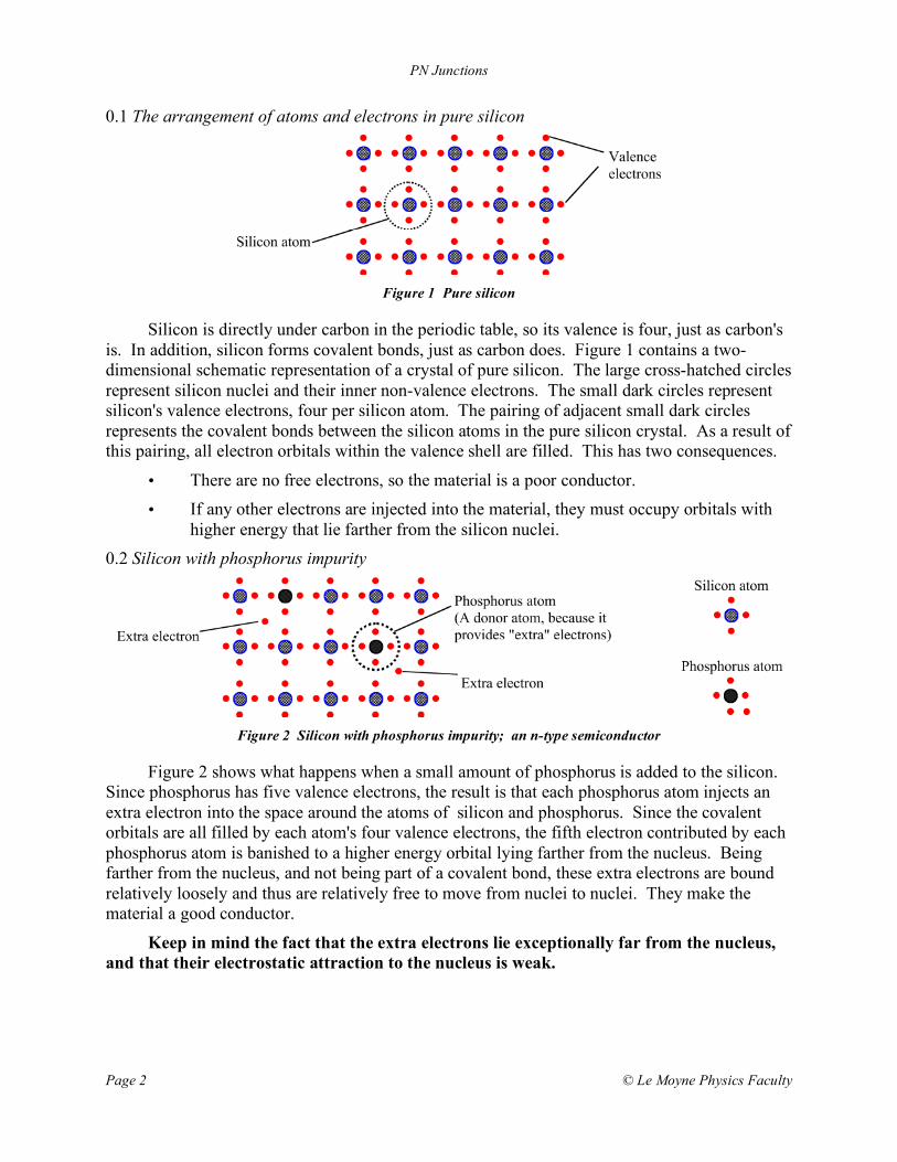
Figure 2 Silicon with phosphorus impurity; an n-type semiconductor
Figure 2 shows what happens when a small amount of phosphorus is added to the silicon. Since phosphorus has five valence electrons, the result is that each phosphorus atom injects an extra electron into the space around the atoms of silicon and phosphorus. Since the covalent orbitals are all filled by each atom's four valence electrons, the fifth electron contributed by each phosphorus atom is banished to a higher energy orbital lying farther from the nucleus. Being farther from the nucleus, and not being part of a covalent bond, these extra electrons are bound relatively loosely and thus are relatively free to move from nuclei to nuclei. They make the material a good conductor.
Keep in mind the fact that the extra electrons lie exceptionally far from the nucleus, and that their electrostatic attraction to the nucleus is weak.
PN Junctions
Page 3 © Le Moyne Physics Faculty
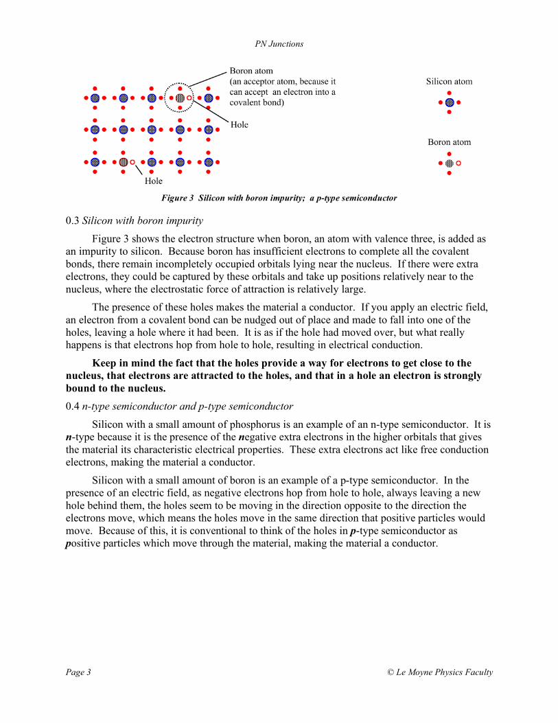
Figure 3 Silicon with boron impurity; a p-type semiconductor
0.3 Silicon with boron impurity
Figure 3 shows the electron structure when boron, an atom with valence three, is added as an impurity to silicon. Because boron has insufficient electrons to complete all the covalent bonds, there remain incompletely occupied orbitals lying near the nucleus. If there were extra electrons, they could be captured by these orbitals and take up positions relatively near to the nucleus, where the electrostatic force of attraction is relatively large. The presence of these holes makes the material a conductor. If you apply an electric field, an electron from a covalent bond can be nudged out of place and made to fall into one of the holes, leaving a hole where it had been. It is as if the hole had moved over, but what really happens is that electrons hop from hole to hole, resulting in electrical conduction.
Keep in mind the fact that the holes provide a way for electrons to get close to the nucleus, that electrons are attracted to the holes, and that in a hole an electron is strongly bound to the nucleus. 0.4 n-type semiconductor and p-type semiconductor
Silicon with a small amount of phosphorus is an example of an n-type semiconductor. It is n-type because it is the presence of the negative extra electrons in the higher orbitals that gives the material its characteristic electrical properties. These extra electrons act like free conduction electrons, making the material a conductor.
Silicon with a small amount of boron is an example of a p-type semiconductor. In the presence of an electric field, as negative electrons hop from hole to hole, always leaving a new hole behind them, the holes seem to be moving in the direction opposite to the direction the electrons move, which means the holes move in the same direction that positive particles would move. Because of this, it is conventional to think of the holes in p-type semiconductor as positive particles which move through the material, making the material a conductor.

PN Junctions
Page 4 © Le Moyne Physics Faculty
0.5 The junction between p-type semiconductor and n-type semiconductor The junction region
-
-
-
-
-
+
+
+
+
+
- -
-
--
+
+
+
+
+
A hole, which acts as if it
were a positive particle
An extra electron
Electric
Field
n-type material p-type material
Negatively charged
acceptor atom (after
accepting an electron)
Positively charged
donor atom (after
losing an electron) Figure 4 A seamless join of p-type and n-type semiconductor material
What happens when p-type semiconductor is joined to n-type semiconductor so seamlessly that the underlying crystal structure is preserved across the join? The extra electrons near the junction between the two material types, which normally are relatively distant from their nuclei and relatively loosely bound, "fall" into the holes, thereby getting closer to a nucleus and becoming more tightly bound. These negative extra electrons "fall" because of the attractive forces from the positively charged nuclei. It also helps that the normal thermal vibration of the atoms of the material help jiggle the extra electrons loose, leaving them unattached and wandering around, so that they by chance encounter and fall into the unoccupied lower orbitals in the p-type material to which they are attracted.
A consequence of the mass movement of the extra electrons from the n-type material to the p-type material is a band of positive charge in the n-type material (because it lost electrons) and a band of negative charge in the p-type material (because it gained electrons). This separation of charge further leads to an electric field pointing from the region of positive charge to the region of negative charge. The regions of positive and negative charge grow in width until the electric field arising from the separated charges becomes strong enough to make it impossible for more electrons to cross the junction from the higher orbitals in the n-type material to the lower orbitals in the p-type material. This will become important below. The final equilibrium state of the junction is summarized in Figure 4. The region near the junction between p-type and n-type material, within which the electric field exists, is an insulator. That is because there are no extra electrons and there are no holes. There are no extra electrons and no holes because the extra electrons from the n-type part of this region have fallen down into the holes, thereby filling the holes. As a result, there are no free charged particles (neither electrons nor holes) which can move in response to an electric field. Therefore, the region around the junction between p-type and n-type material is an insulator.

PN Junctions
Page 5 © Le Moyne Physics Faculty
A seamless join of p-type and n-type material is known as a semiconductor diode. As will be described in the sections that follow, a semiconductor diode is a one-way street for electrical current: electrical current can flow one way through the diode but not the other. 0.6 A reverse-biased PN junction
+ hole
+ +
+ +
- - -
- -
+
-
-
+
+ -
Total Electric-field: internal + battery
E-field from
battery wires
extra electron
Internal
E-field
Figure 5 When a battery is connected to a diode as shown here (negative wire to p-type material and positive wire to n-type material), the connection is called "reverse-biased."
Figure 5 shows a semiconductor diode connected to a battery, with the negative terminal of the battery connected to the p-type semiconductor and the positive terminal of the battery connected to the n-type semiconductor. This connection of a battery to a diode is called reverse-biased. Note that the electrical field between the battery terminals (being from plus to minus) is in the same direction as the internal field in the diode and adds to the existing electric field. Also, the negative wire from the battery injects electrons into the p-type material, filling in more of the holes and extending the width of the negative charge layer, while the positive terminal from the battery sucks negative electrons out of the n-type region, extending the width of the positive charge layer. Within these charged layers empty holes, which enable conduction in p-type material, are absent, and extra electrons, which enable conduction in n-type material, are absent. The battery has caused the total width of the insulating region that surrounds the junction between p-type and n-type material to become wider. Before the battery was connected, the junction region of the diode was a non-conductor for lack of mobile electrons and holes; after the battery is connected in reverse bias, that region is an even bigger and better non-conductor. Conclusion In a reverse-bias connection, current does not flow through a diode.
In reality, a little current will flow. This is because of the thermal vibration of the atoms, which shakes things up enough so that some electrons can move from the negative wire to the positive wire. However, the current is very small, typically on the order of 1 nA (10-9 amperes). 0.7 A forward-biased PN junction
Figure 6 shows a forward-biased PN junction, a diode in which the positive terminal of a battery is connected to the p-type material and the negative battery terminal is connected to the n-type material. Now the E-field from the battery wires opposes and cancels out the internal E-

PN Junctions
Page 6 © Le Moyne Physics Faculty
field of the diode, making the total local electric field nearly zero or in the direction opposite to the direction of the original local electric field.
+ hole
+ +
+ +
- - -
- -
+
-
-
+
E
+ -
Total E-field: internal + battery
E-field from
battery wires
extra electron
Internal
E-field
Figure 6 When a battery is connected to a diode as shown here (positive wire to p-type
material and negative wire to n-type material), the connection is called "forward-biased."
It was the internal E-field that, in a diode not connected to a battery, had opposed and finally stopped the transfer of extra electrons across the junction into holes. That internal E-field is now erased, and there is nothing to stop extra electrons from cascading from higher n-type orbitals down to lower unfilled p-type orbitals, and so current flows in a gush. Electrons that fall over the junction are replaced from the wire connected to the negative terminal of the battery. After falling over the junction, they flow from hole to hole toward the wire connected to the positive terminal of the battery and ultimately back to the battery.
Conclusion In a forward-bias connection, current flows easily through a diode. In a light emitting diode (LED), when the electron falls through the junction, from a higher orbital into a vacancy in a lower orbital, the energy released in the transition appears as light. 0.8 The circuit symbol for a diode
The circuit symbol for a diode is a triangle with a bar on one vertex, as shown in Figure 7 part (b).
+
+ +
+
+
- - -
- -
+
-
-
+
E-field
(b) The symbol used to represent a
diode in an electronic circuit.
(a) The physical structure of a diode
Figure 7 The relation between a diode's physical structure and its circuit symbol
The triangle points in the direction in which a diode allows current to flow. See Figure 8.

PN Junctions
Page 7 © Le Moyne Physics Faculty
+
I = 0 amperes
+ - I
(b) A reverse-biased diode. The battery
would have current flow counter-
clockwise, but the diode does not allow
current to flow opposite the direction in
which the triangle points.
(a) A forward-biased diode. Current
flows easily in the direction shown
(the direction in which the triangle
points).
I
-
Figure 8 The two ways to connect a diode to a battery
Equipment: Computer with MS Excel 97 Banana plug test board pre-wired with red, green, & blue LEDs and 1 kΩ resistor See Figure 9 on page 7. Red, green, and blue LEDs (clear case, at least 10 mA; mounted on test board) Sample Radio Shack LED part numbers: 276-309(red), 276-303(green), 276-311(blue) 1 KΩ resistor, 1/4 Watt (mounted on test board) An extra, unconnected LED, for easy visual inspection Variable DC Power Supply (0 V to 10 V, at least 10 mA) Voltmeter (having a 2 V or 3 V range with 4 significant digits) Ammeter (at least 3 significant digits; 2 mA & 20 mA ranges, or 3 mA & 30 mA) Banana plug wire connectors Magnifying glass (a convex lens will suffice)
Figure 9 The banana plug test board used in these lab activities. Note the 1 kΩ resistor and the three LEDs.
PN Junctions
Page 8 © Le Moyne Physics Faculty
1. Activity #1: Instructor explains Figures 1 - 6 This is done with a view to preparing lab participants to answer question Q5.
2. Activity #2: Examine the LED Abstract Using a magnifying glass, examine the various parts of an LED.
2.1 LED is an acronym for light emitting diode. A diode is a one-way flow control for electricity. A light emitting diode is a diode that is designed to emit light. 2.2 Use the magnifying glass to examine the diode that is not connected to the banana plug test board. The two wires coming out of the LED are called its leads. Follow the leads inside the LED, and note where they go. Also note that one lead is shorter than the other.
Q 1 In the space below, sketch the LED, and describe each of the LED's internal parts. Include in your description the shape of the internal parts (a drawing is a very good idea), and indicate what the parts might be made of (metal, plastic or glass, other ...). 3. Activity #3: The forward-biased I-V curve for an LED Abstract Measure and graph the current through a diode versus voltage across a diode when the diode is forward-biased.
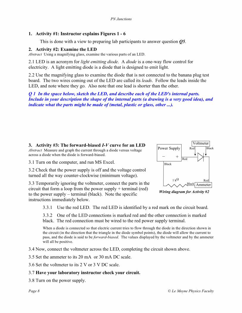
3.1 Turn on the computer, and run MS Excel. 3.2 Check that the power supply is off and the voltage control turned all the way counter-clockwise (minimum voltage). 3.3 Temporarily ignoring the voltmeter, connect the parts in the circuit that form a loop from the power supply + terminal (red) to the power supply – terminal (black). Note the specific instructions immediately below.
3.3.1 Use the red LED. The red LED is identified by a red mark on the circuit board.
3.3.2 One of the LED connections is marked red and the other connection is marked black. The red connection must be wired to the red power supply terminal. When a diode is connected so that electric current tries to flow through the diode in the direction shown in the circuit (in the direction that the triangle in the diode symbol points), the diode will allow the current to pass, and the diode is said to be forward-biased. The values displayed by the voltmeter and by the ammeter will all be positive.
3.4 Now, connect the voltmeter across the LED, completing the circuit shown above.
3.5 Set the ammeter to its 20 mA or 30 mA DC scale. 3.6 Set the voltmeter to its 2 V or 3 V DC scale.
3.7 Have your laboratory instructor check your circuit. 3.8 Turn on the power supply.
1 k!
Black Red
Red
Power Supply
Wiring diagram for Activity #2
– +
Black Red
Voltmeter
Ammeter
Black
PN Junctions
Page 9 © Le Moyne Physics Faculty
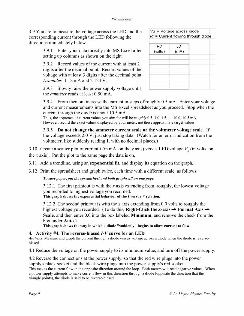
3.9 You are to measure the voltage across the LED and the corresponding current through the LED following the directions immediately below.
3.9.1 Enter your data directly into MS Excel after setting up columns as shown on the right. 3.9.2 Record values of the current with at least 2 digits after the decimal point. Record values of the voltage with at least 3 digits after the decimal point. Examples 1.12 mA and 2.123 V. 3.9.3 Slowly raise the power supply voltage until the ammeter reads at least 0.50 mA. 3.9.4 From then on, increase the current in steps of roughly 0.5 mA. Enter your voltage and current measurements into the MS Excel spreadsheet as you proceed. Stop when the current through the diode is about 10.5 mA. Thus, the sequence of current values you aim for will be roughly 0.5, 1.0, 1.5, ..., 10.0, 10.5 mA. However, record the exact values displayed by your meter, not these approximate target values.
3.9.5 Do not change the ammeter current scale or the voltmeter voltage scale. If the voltage exceeds 2.0 V, just stop taking data. (Watch for an error indication from the voltmeter, like suddenly reading 1. with no decimal places.)
3.10 Create a scatter plot of current I (in mA, on the y axis) versus LED voltage Vd (in volts, on the x axis). Put the plot to the same page the data is on. 3.11 Add a trendline, using an exponential fit, and display its equation on the graph.
3.12 Print the spreadsheet and graph twice, each time with a different scale, as follows: To save paper, put the spreadsheet and both graphs all on one page.
3.12.1 The first printout is with the x axis extending from, roughly, the lowest voltage you recorded to highest voltage you recorded. This graph shows the exponential behavior of the I versus V relation.
3.12.2 The second printout is with the x axis extending from 0.0 volts to roughly the highest voltage you recorded. (To do this, Right-Click the x-axis → Format Axis → Scale, and then enter 0.0 into the box labeled Minimum, and remove the check from the box under Auto.) This graph shows the way in which a diode "suddenly" begins to allow current to flow.
4. Activity #4: The reverse-biased I-V curve for an LED Abstract Measure and graph the current through a diode versus voltage across a diode when the diode is reverse-biased.
4.1 Reduce the voltage on the power supply to its minimum value, and turn off the power supply.
4.2 Reverse the connections at the power supply, so that the red wire plugs into the power supply's black socket and the black wire plugs into the power supply's red socket. This makes the current flow in the opposite direction around the loop. Both meters will read negative values. When a power supply attempts to make current flow in this direction through a diode (opposite the direction that the triangle points), the diode is said to be reverse-biased.
Vd = Voltage across diode
Id = Current flowing through diode
Vd Id
(volts) (mA)

PN Junctions
Page 10 © Le Moyne Physics Faculty
4.3 Change to voltmeter to the 20 V DC scale, but leave the ammeter on the 20 mA DC scale. 4.4 Fill in the current values corresponding to the values in the table below. Do not use MS Excel; do not make a graph.
To see that the ammeter is working, change to the lowest current scale, and vary the voltage between 1.5 V and 5.0 V, noting that the current also varies. Then reset the ammeter to the 20 mA scale.
Vd (LED voltage) (volts)
Id (LED current) (mA)
-1.5
-2.0
-2.5
-3.0
-3.5
-4.0
-4.5
-5.0
Q 2 Refer to the graphs you made and to the table immediately above. Based on these, give a succinct but complete characterization of the way your LED responds to applied voltages.
5. Activity #5: Relation between LED turn-on voltage and color of emitted light Abstract Determine the electron energy required to produce three different colors of light. 5.1 Reduce the voltage on the power supply to its minimum value, and turn off the power supply. 5.2 Connect the circuit for Activity #4. It is the same as the circuit for Activity #2 except the ammeter is left out. 5.3 Turn on the power supply.
5.4 Slowly increase the power supply voltage until the LED just barely starts to glow. Record this voltage, Von, in the table below. You get the best view of the LED if you look directly into the round top of the plastic dome.
1 k!
Red
Power Supply
Wiring diagram for Activity #4
– +
Black Red
Voltmeter
Black

PN Junctions
Page 11 © Le Moyne Physics Faculty
5.5 Reduce the voltage on the power supply to its minimum value, turn off the power supply, remove the LED, replace it with another, and then repeat 5.4. Do the same with the third LED.
5.6 Use E = q V, with q = 1.6 × 10⁻¹⁹ coulombs (the magnitude of the electron charge), to find the energy that single electrons lose when forced through the LEDs just at the point that they are beginning to produce red, green, or blue light. Write the values in the table below.
LED Color
Von (Volts)
Single Electron Energy (joules)
Red
Green
Blue
Q 3 What happens to the energy an electron loses when it passes through an LED.
Q 4 What do the data in the above table, together with your answer to Q 3, tell you about red, green, and blue light? (To answer this question, just state your conclusion; you do not need to explain it.)
PN Junctions
Page 12 © Le Moyne Physics Faculty
Q 5 In the space below, explain in your own words why a diode allows electric current to flow freely in one direction but almost completely prohibits the flow of current in the other direction. You may consult with your lab partners while developing your response. Diagrams are very helpful to make clear what you are saying.
PN Junctions
Page 13 © Le Moyne Physics Faculty
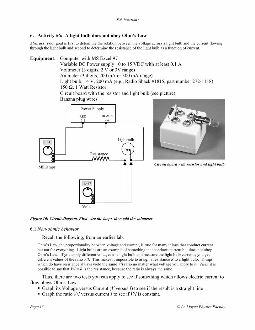
6. Activity #6: A light bulb does not obey Ohm's Law Abstract Your goal is first to determine the relation between the voltage across a light bulb and the current flowing through the light bulb and second to determine the resistance of the light bulb as a function of current.
Equipment: Computer with MS Excel 97 Variable DC Power supply: 0 to 15 VDC with at least 0.1 A Voltmeter (3 digits, 2 V or 3V range) Ammeter (3 digits, 200 mA or 300 mA range) Light bulb: 14 V, 200 mA (e.g., Radio Shack #1815, part number 272-1118) 150 Ω, 1 Watt Resistor Circuit board with the resistor and light bulb (see picture) Banana plug wires
61.4
1.447
Volts
Milliamps
Resistance
Lightbulb
Power Supply
RED (-)
BLACK
(+)
Figure 10: Circuit diagram. First wire the loop; then add the voltmeter
6.1 Non-ohmic behavior
Recall the following, from an earlier lab. Ohm’s Law, the proportionality between voltage and current, is true for many things that conduct current but not for everything. Light bulbs are an example of something that conducts current but does not obey Ohm’s Law. If you apply different voltages to a light bulb and measure the light bulb currents, you get different values of the ratio V/I. This makes it impossible to assign a resistance R to a light bulb. Things which do have resistance always yield the same V/I ratio no matter what voltage you apply to it. Then it is possible to say that V/I = R is the resistance, because the ratio is always the same.
Thus, there are two tests you can apply to see if something which allows electric current to flow obeys Ohm's Law:
Graph its Voltage versus Current (V versus I) to see if the result is a straight line Graph the ratio V/I versus current I to see if V/I is constant.
Circuit board with resistor and light bulb

PN Junctions
Page 14 © Le Moyne Physics Faculty
A A . or
V V . or
When the above tests succeed (V versus I is a straight line and V/I is constant), the device is called ohmic, because it obeys Ohm's Law. When these two tests fail, the device does not obey Ohm's Law and is called non-ohmic. The I versus V graphs you just completed for a diode show that diodes are non-ohmic. In this activity, you apply both of the tests for non-ohmic behavior to a light bulb. 6.2 Construct the circuit
6.2.1 Make sure that the power supply is switched off and the voltage control knob on the power supply is set at its minimum position by turning it counterclockwise all the way. 6.2.2 Construct the circuit in Figure 10.
6.2.3 Have your lab instructor check your circuit before proceeding any further.
Current Voltage Current Resistance (amperes) (volts) (amperes) (ohms)
0.00 0.00 empty empty
... ... ... ...
... ... ... ... Figure 11 Example of how to organize the spreadsheet. Use spreadsheet formulae to copy the values of the current from the left column into the column next to Resistance. Resistance values are calculated using Ohm's Law.
6.3 Collect data
6.3.1 Turn on the computer, run MS Excel. 6.3.2 Set the voltmeter to the 2 or 3 V DC scale. On the meter, look for
6.3.3 Set the ammeter to the 200 or 300 mA DC scale. Look for 6.3.4 Turn on the power supply. Now you are ready to collect data.
6.3.5 During data collection, the bulb will not light, though the filament may glow a little at high current. Do not be concerned if your light bulb does not glow.
6.3.6 Make your first entry into your spreadsheet a current of 0.0 A with a corresponding voltage of 0.0 V. You do not need to measure this. No voltage means there will be no current. 6.3.7 Next, adjust the voltage control knob on the power supply to set the current at about 5.0 mA, and enter the actual current in amperes (not in mA) and voltage in volts from the meters into your spreadsheet. [If the current will not go as low as 5.0 mA, just use the lowest current you can get.] 6.3.8 Next, adjust the current to about 15 mA, and enter the actual current in amperes and voltage in volts from the meters into your spreadsheet. 6.3.9 To continue, increase the current by about 10 mA, and enter the actual current in amperes and voltage in volts from the meters into your spreadsheet. Repeat this until you

PN Junctions
Page 15 © Le Moyne Physics Faculty
have collected a total of nine current-voltage pairs. (The nine currents, in amperes, will be approximately 0.000, 0.005, 0.015, 0.025, 0.035, 0.045, 0.055, 0.065, 0.075.) If the voltage exceeds 2.0 volts (indicated by a display that reads 1.), just stop taking data and continue with the next part of the lab activity.
6.4 Graph light bulb Voltage versus Current Create a scatter plot of the light bulb current in amperes on the horizontal axis and the voltage in volts on the vertical axis. Putting the plot on the spreadsheet page instead of on a separate page is preferred.
6.5 Graph light bulb Resistance versus Current 6.5.1 You cannot calculate a resistance from 0.0 amperes and 0.0 volts, so ignore the first pair of data points when calculating resistance. 6.5.2 Make columns containing light bulb Current in amperes (copied from the original data using spreadsheet formulae) and light bulb Resistance in ohms (calculated using spreadsheet formulae).
6.5.3 Create a scatter plot of the light bulb current in amperes on the horizontal axis and the light bulb resistance in ohms on the vertical axis. Putting the plot on the spreadsheet page instead of on a separate page is preferred, but either way is fine.
6.6 Print a copy of the spreadsheet for everybody in your group.
Q 6 Using only the light bulb Voltage versus Current graph (the first graph that you made), does the light bulb obey Ohm's Law or does it not obey Ohm's Law? Justify your answer using your graph.
Q 7 Using only the light bulb Resistance versus Current graph (the second graph that you made), does the light bulb obey Ohm's Law or does it not obey Ohm's Law? Justify your answer using your graph.

PN Junctions
Page 16 © Le Moyne Physics Faculty
7. What to hand in ... • This handout, with all questions answered • Printout of the diode spreadsheet, containing the original data plus two I versus V graphs
(see 3.12.1 and 3.12.2) • Printout of the light bulb spreadsheet, containing the original data plus the V versus I graph
(6.4) and the R versus I graph (6.5)

PN Junctions
Page 17 © Le Moyne Physics Faculty
Pre-Lab Questions Print Your Name ______________________________________ Read the Introduction to this handout, and answer the following questions before you come to General Physics Lab. Write your answers directly on this page. When you enter the lab, tear off this page and hand it in.
1. What does a one-way valve, also known as a check valve, do?
2. What does a diode do?
3. In the context of PN junctions, what is a hole?
4. How does electricity flow through n-type semiconductor material?
5. How does electricity flow through p-type semiconductor material?
6. Energy is released when an electron crosses a PN junction from the n-type material to the p-type material. Explain, in terms of electron orbitals, what the electron does that causes energy to be emitted in the form of light (in the case of light emitting diodes).
7. Explain why the region of positive and negative charge in a diode is an insulator.
8. Tell what you have to do to convert the region of positive and negative charge in a diode into a conductor.
Continued on the next page ...

PN Junctions
Page 18 © Le Moyne Physics Faculty
9. Draw a circuit showing a diode connected to a battery so that current flows around the circuit. Use the electronic symbols for a diode and for a battery.
10. What two tests can one apply to a device that conducts electricity to determine whether or not it obeys Ohm's Law? (Section 6.1)
11. Draw and explain the physical construction of a diode. You do not need to explain how a diode does what it does; just show how it is made.