Lecture 7 pn Junctions - alexu.edu.eg
26
Lecture 7 pn Junctions pn junctions 1-1 Sunday 8/10/2016
Transcript of Lecture 7 pn Junctions - alexu.edu.eg
Lecture 7
pn Junctions
pn junctions 1-1 Sunday 8/10/2016
Outline Voltage regulator (Zener diodes) Clipping and clamping circuits Voltage Multiplier Circuits
pn junctions 1-2
pn junctions 1-3
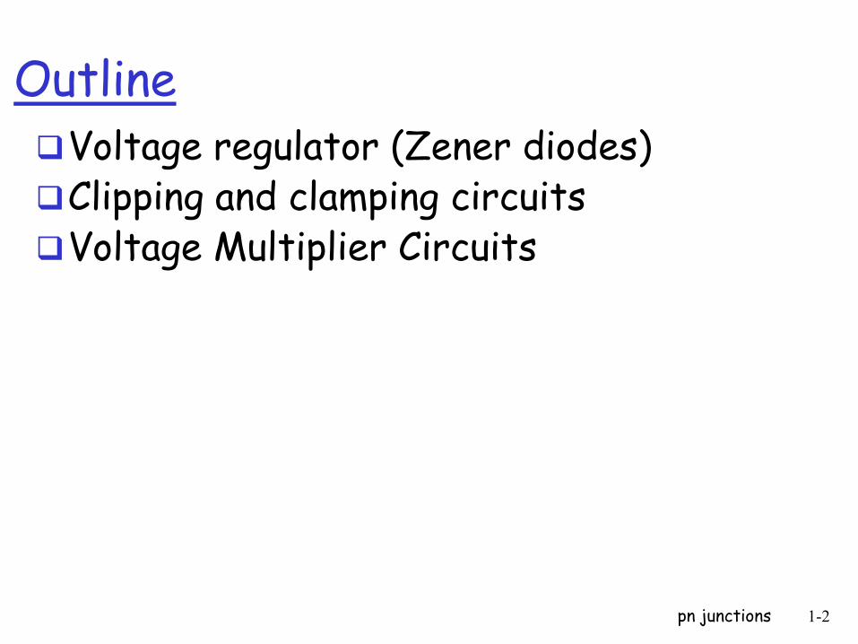
Voltage Regualtor
Function: to maintain a constant voltage across the load when the source voltage or the load current varies
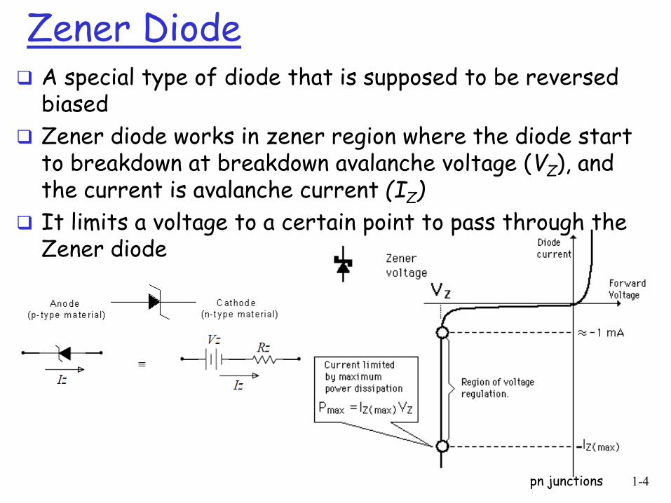
Zener Diode A special type of diode that is supposed to be reversed
biased
Zener diode works in zener region where the diode start to breakdown at breakdown avalanche voltage (VZ), and the current is avalanche current (IZ)
It limits a voltage to a certain point to pass through the Zener diode
pn junctions 1-4
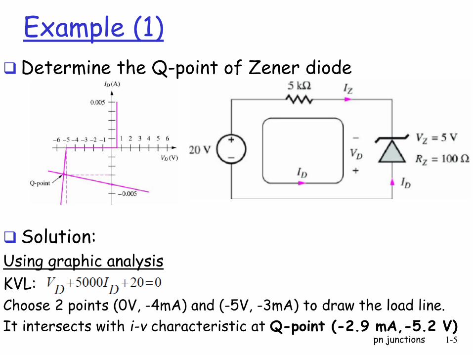
Example (1)
Determine the Q-point of Zener diode
Solution: Using graphic analysis
KVL: Choose 2 points (0V, -4mA) and (-5V, -3mA) to draw the load line.
It intersects with i-v characteristic at Q-point (-2.9 mA,-5.2 V)
pn junctions 1-5
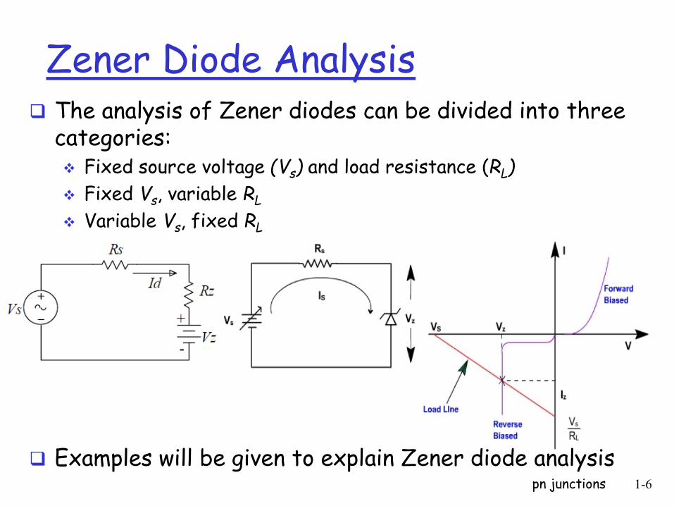
Zener Diode Analysis The analysis of Zener diodes can be divided into three
categories: Fixed source voltage (Vs) and load resistance (RL)
Fixed Vs, variable RL
Variable Vs, fixed RL
Examples will be given to explain Zener diode analysis pn junctions 1-6
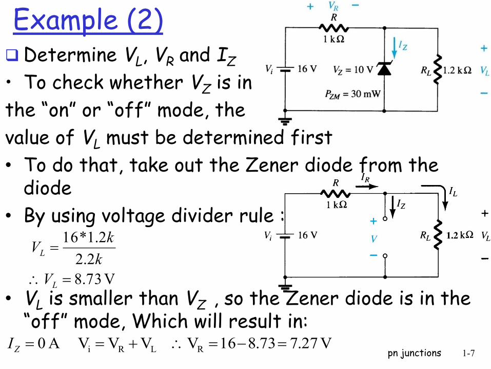
Example (2) Determine VL, VR and IZ
• To check whether VZ is in
the “on” or “off” mode, the
value of VL must be determined first
• To do that, take out the Zener diode from the diode
• By using voltage divider rule :
• VL is smaller than VZ , so the Zener diode is in the “off” mode, Which will result in:
pn junctions 1-7
V 73.8
2.2
2.1*16
L
L
V
k
kV
A 0ZI V 27.773.816VVVV RLRi
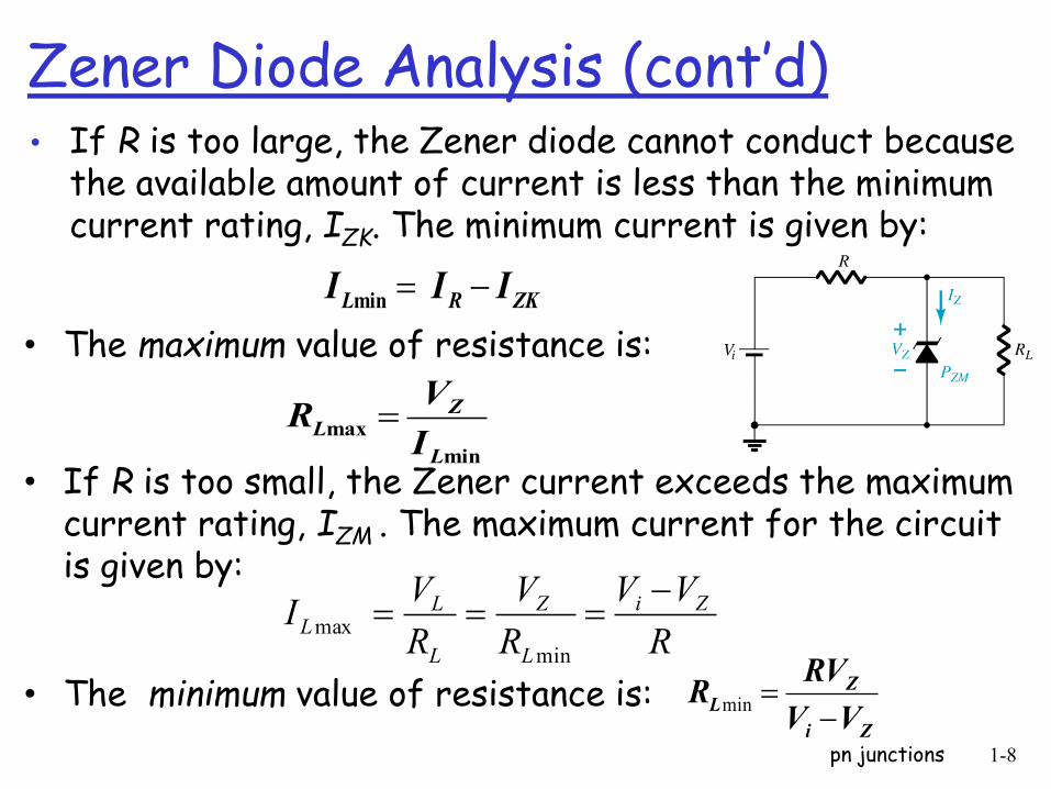
Zener Diode Analysis (cont’d) • If R is too large, the Zener diode cannot conduct because
the available amount of current is less than the minimum current rating, IZK. The minimum current is given by:
pn junctions 1-8
ZKRL I II min
• The maximum value of resistance is:
min
max L
ZL
I
VR
• If R is too small, the Zener current exceeds the maximum current rating, IZM . The maximum current for the circuit is given by:
R
VV
R
V
R
V I Zi
L
Z
L
LL
min
max
• The minimum value of resistance is: Zi
ZL
VV
RVR
min
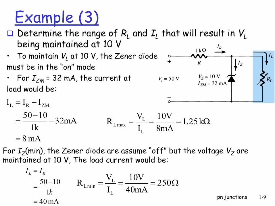
Example (3) Determine the range of RL and IL that will result in VL
being maintained at 10 V • To maintain VL at 10 V, the Zener diode
must be in the “on” mode
• For IZM = 32 mA, the current at
load would be:
pn junctions 1-9
mA 8
mA32k1
1050
III ZMRL
k 25.1mA8
V10
I
VR
L
LmaxL
For IZ(min), the Zener diode are assume “off” but the voltage VZ are maintained at 10 V, The load current would be:
mA 40
1
1050
k
II RL
250mA40
V10
I
VR
L
LminL
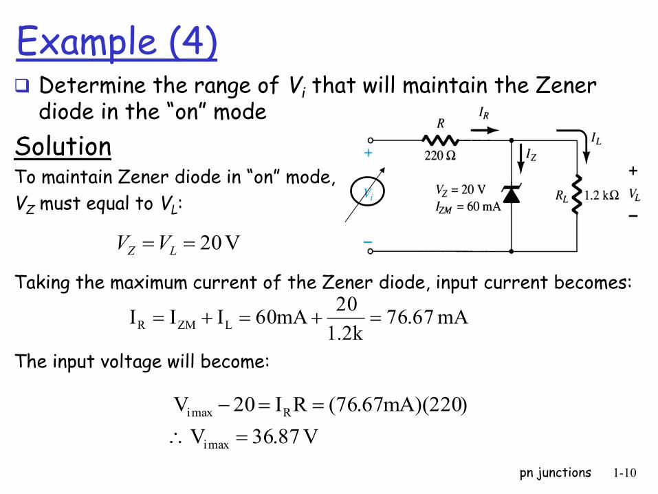
Example (4) Determine the range of Vi that will maintain the Zener
diode in the “on” mode
Solution To maintain Zener diode in “on” mode,
VZ must equal to VL:
Taking the maximum current of the Zener diode, input current becomes:
The input voltage will become:
pn junctions 1-10
V 20 LZ VV
mA 67.76k2.1
20mA60III LZMR
V 87.36V
)220)(mA67.76(RI20V
maxi
Rmaxi
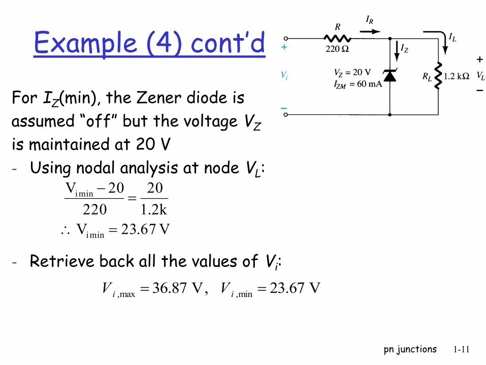
Example (4) cont’d
For IZ(min), the Zener diode is
assumed “off” but the voltage VZ
is maintained at 20 V
- Using nodal analysis at node VL:
- Retrieve back all the values of Vi:
pn junctions 1-11
V 67.23V
k2.1
20
220
20V
mini
mini
,max ,min36.87 V, 23.67 Vi iV V
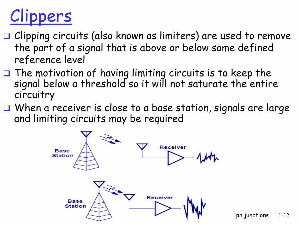
Clippers Clipping circuits (also known as limiters) are used to remove
the part of a signal that is above or below some defined reference level
The motivation of having limiting circuits is to keep the signal below a threshold so it will not saturate the entire circuitry
When a receiver is close to a base station, signals are large and limiting circuits may be required
pn junctions 1-12
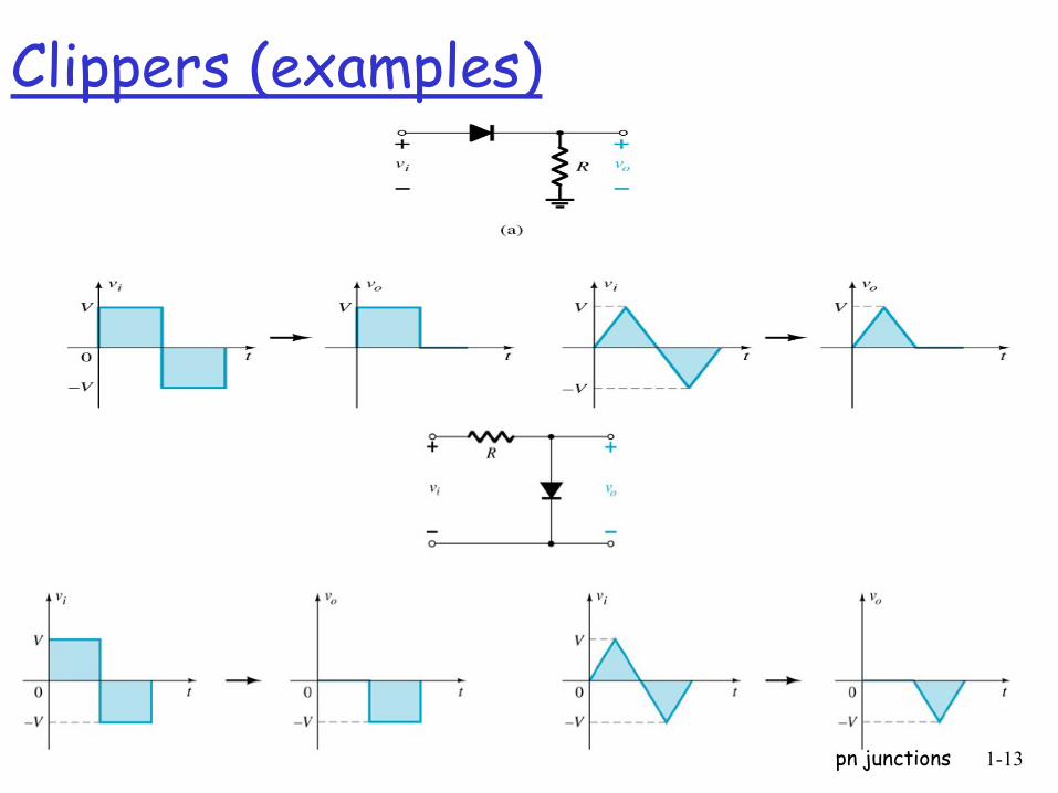
Clippers (examples)
pn junctions 1-13
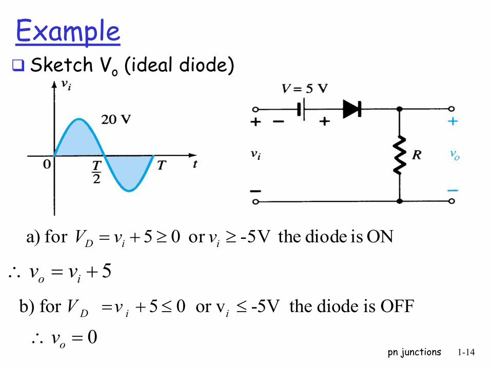
Example Sketch Vo (ideal diode)
pn junctions 1-14
ON is diode the-5Vor 05 for a) iiD vvV
5 io vv
b) for 5 0 or v -5V the diode is OFFD i iV v
0 ov
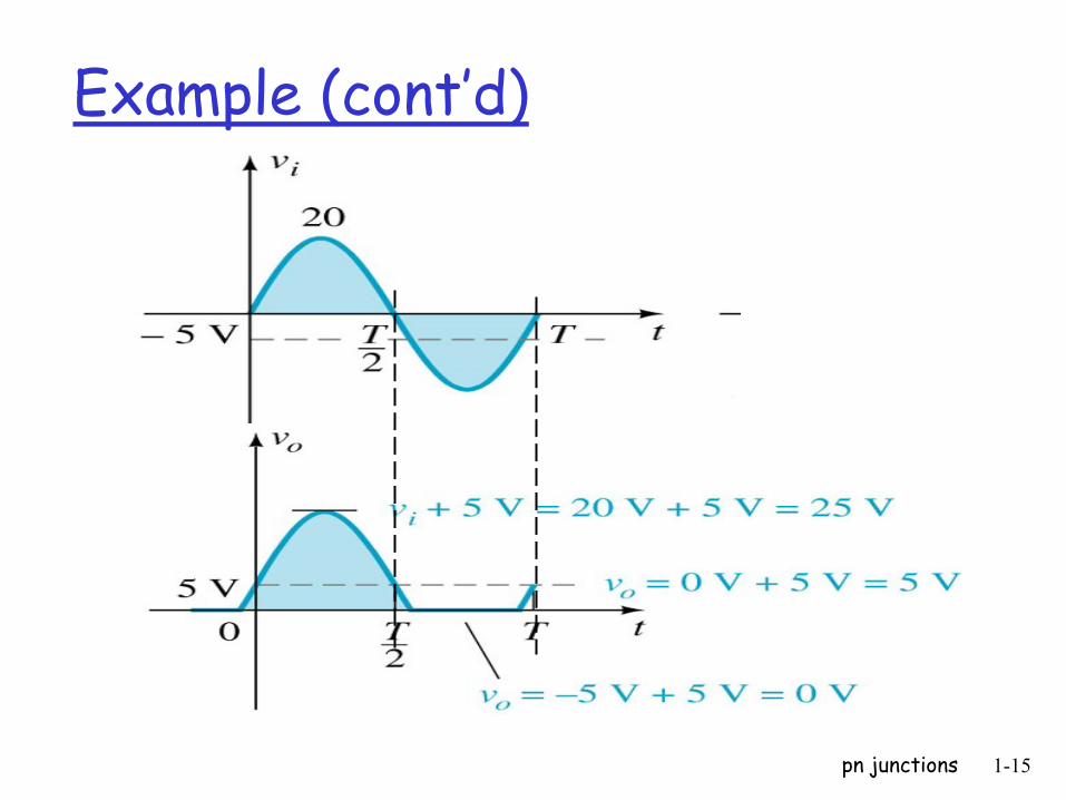
Example (cont’d)
pn junctions 1-15
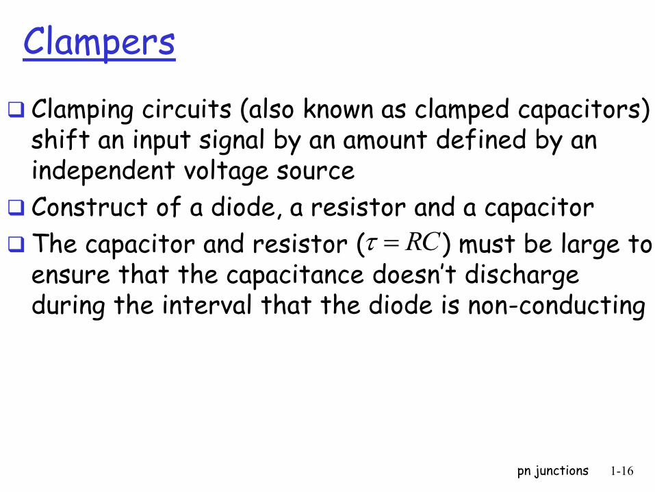
Clampers
Clamping circuits (also known as clamped capacitors) shift an input signal by an amount defined by an independent voltage source
Construct of a diode, a resistor and a capacitor
The capacitor and resistor ( ) must be large to ensure that the capacitance doesn’t discharge during the interval that the diode is non-conducting
pn junctions 1-16
RC
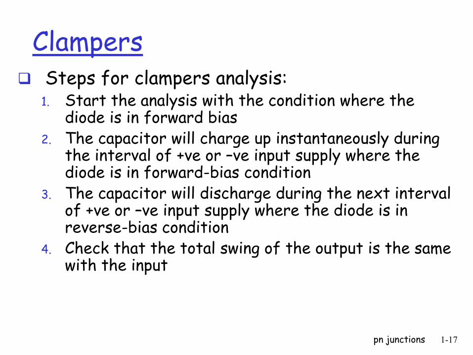
Clampers Steps for clampers analysis:
1. Start the analysis with the condition where the diode is in forward bias
2. The capacitor will charge up instantaneously during the interval of +ve or –ve input supply where the diode is in forward-bias condition
3. The capacitor will discharge during the next interval of +ve or –ve input supply where the diode is in reverse-bias condition
4. Check that the total swing of the output is the same with the input
pn junctions 1-17
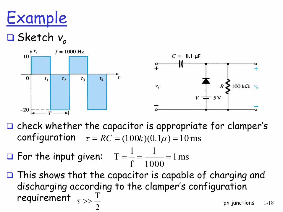
Example Sketch vo
check whether the capacitor is appropriate for clamper’s configuration
For the input given:
This shows that the capacitor is capable of charging and discharging according to the clamper’s configuration requirement
pn junctions 1-18
ms 10)1.0)(100( kRC
ms 11000
1
f
1T
2
T
0.1 μF
Example (cont’d)
pn junctions 1-19
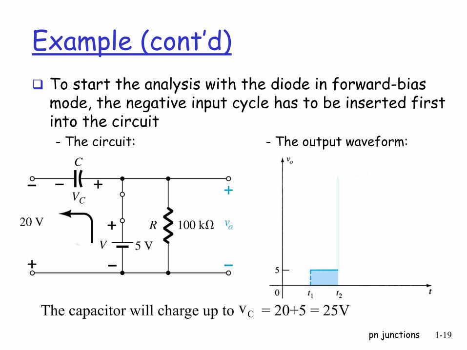
To start the analysis with the diode in forward-bias mode, the negative input cycle has to be inserted first into the circuit - The circuit: - The output waveform:
The capacitor will charge up to = 20+5 = 25V Cv
Example (cont’d)
pn junctions 1-20
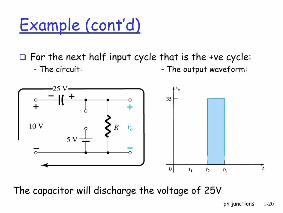
For the next half input cycle that is the +ve cycle: - The circuit: - The output waveform:
The capacitor will discharge the voltage of 25V
Example (cont’d)
pn junctions 1-21
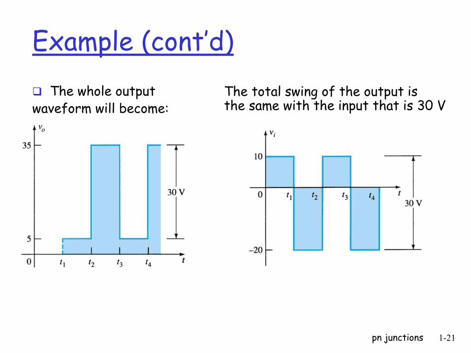
The whole output waveform will become:
The total swing of the output is the same with the input that is 30 V
Voltage Multipliers Using clamping circuits (increase peak of
rectified circuits)
Used in high voltage low current applications such as cathode-ray tubes (CRTs) and particle accelerators
Circuits: Voltage doublers
Voltage triplers
Voltage quadruplers
pn junctions 1-22
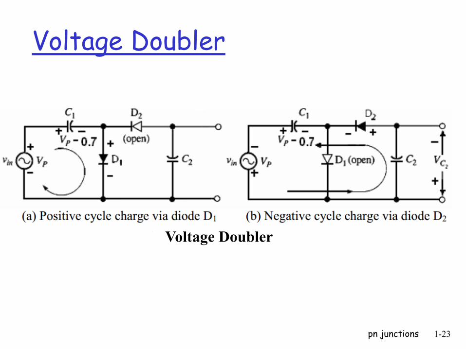
Voltage Doubler
pn junctions 1-23
Voltage Doubler
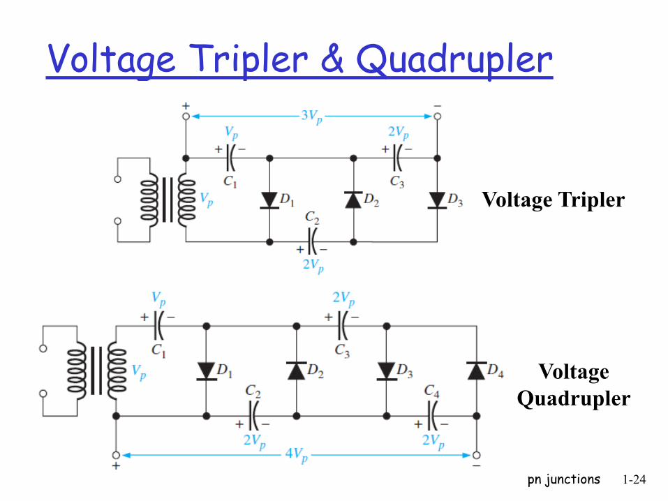
Voltage Tripler & Quadrupler
pn junctions 1-24
Voltage Tripler
Voltage
Quadrupler
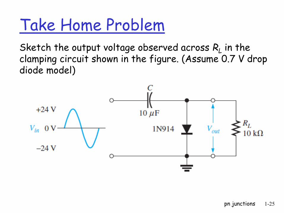
Take Home Problem
pn junctions 1-25
Sketch the output voltage observed across RL in the clamping circuit shown in the figure. (Assume 0.7 V drop diode model)
pn junctions 1-26
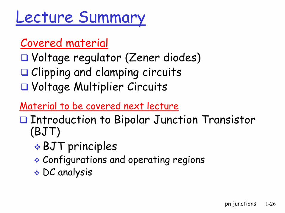
Lecture Summary
Covered material Voltage regulator (Zener diodes) Clipping and clamping circuits Voltage Multiplier Circuits
Material to be covered next lecture
Introduction to Bipolar Junction Transistor (BJT) BJT principles Configurations and operating regions DC analysis