10 Steps to Increase HDI Membership - South Florida HDI Local Chapter
Upload
sierra-circuits-incCategory
view
383download
5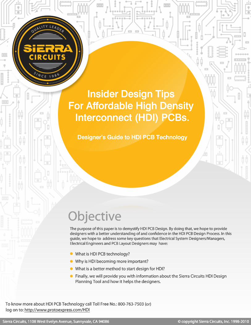
ObjectiveThe purpose of this paper is to demystify HDI PCB Design. By doing that, we hope to provide designers with a better understanding of and confidence in the HDI PCB Design Process. In this guide, we hope to address some key questions that Electrical System Designers/Managers, Electrical Engineers and PCB Layout Designers may have:
What is HDI PCB technology?
Why is HDI becoming more important?
What is a better method to start design for HDI?
Finally, we will provide you with information about the Sierra Circuits HDI Design Planning Tool and how it helps the designers.
Insider Design Tips For Affordable High Density Interconnect (HDI) PCBs.
Designer’s Guide to HDI PCB Technology
Sierra Circuits, 1108 West Evelyn Avenue, Sunnyvale, CA 94086 © copyright Sierra Circuits, Inc. 1998-2010
Insider Design Tips to an Affordable High Density Interconnect (HDI) PCB
Designer’s Guide to HDI PCB Technology
Sierra Circuits, 1108 West Evelyn Avenue, Sunnyvale, CA 94086 © copyright Sierra Circuits, Inc. 1998-2010
What is HDI? HDI stands for HIGH DENSITY INTERCONNECT. As the name suggests, an HDI PCB is characterized by its high density of components and routing interconnections that use the latest PCB technologies. An HDI design is by its very nature a high performance design.
HDI design uses the latest advances in the PCB interconnection technology. HDI design uses the latest advances in the PCB interconnection technology. Keeping in mind the latest state of the art PCB technology, we can define the HDI PCBs as those printed circuit boards that use some or all of these features: microvias, blind and buried vias/microvias techniques, built-up PCB laminations and high signal performance considerations.
One of the key driving factors is to achieve more connections per area of the Printed Circuit Board. This results in a more compact, dense, and lower layer count PCBs.
Not only does it make the PCBs smaller, lighter, and thinner; but HDI PCBs provide a much superior electrical performance. Including:
Better Electrical performance and signal integrity
Lower Noise and crosstalk; Lower EMI/RFI
Smaller Size and Weight.
Cost Optimization: HDI design reduces overall cost by decreasing the number of layers and size as compared to a STANDARD TECHNOLOGY PCB design for the same level of complexity
ReducedReduced Design Time: HDI technology allows for more real estate on the board which results in faster signal routing during the layout design stage
More Reliable Designs: Studies conducted by IPC and other industry organizations have talked about superior reliability of small-blind vias over TH vias. This is due to the fact that the via aspect ratio (AR-depth to diameter ratio) is less than1:1 compared to TH which has an AR greater than 6:1 that goes as high as 20:1.
Advantages of HDI:

Insider Design Tips to an Affordable High Density Interconnect (HDI) PCB
Designer’s Guide to HDI PCB Technology
Sierra Circuits, 1108 West Evelyn Avenue, Sunnyvale, CA 94086 © copyright Sierra Circuits, Inc. 1998-2010
What is driving the increased preference for HDI?
Complex and Dense Devices: High pin count and high density device packages such as ball grid arrays (BGA), chip-scale packaging (CSP), Wirebond and Flip chip BGAs, chip-on-board (COB), and system-in-package (SiP) are leading factors. When a complex and dense device has a large pin count and a very low pitch, it is almost impossible to design a PCB with a reasonable number of layers and/or thickness using standard PCB technology. The solution? HDI!
CompactCompact PCBs: As everything gets smaller, faster and cheaper at an ever increasing rate, the designers are faced with increasingly smaller PCB sizes and a reduced number of PCB layers. If one were to use conventional non-HDI designs, many would require a large number of PCB layers. HDI provides a smarter solution.
Integrating several PCBs into a single PCB: With HDI, several existing PCBs can be integrated into a single high density PCB in a more efficient manner.
SignalSignal Integrity Discipline: As PCBs have incorporated circuits that require higher speed signal transitions, faster rise times, and higher clock rates, it has required even higher signal integrity levels and electrical performance requirements. These require a high degree of Signal Integrity Discipline to be implemented during PCB Design and Manufacturing, which HDI provides.
Making HDI work for you- The First Step!
AA good rule of thumb is to ask yourself, “Is HDI PCB technology going to solve a real problem and serve a real purpose in my design?” You should know exactly why you need HDI PCB technology in your PCB at the very beginning of the design process. We’ve provided some examples of when you should consider HDI PCB technology. Whatever your reasons, it is imperative that you be very clear about what these are from the very start!
Once you’ve tackled the first step, we hope you will find the following design recipe from us very useful.
PCB designers cite the following reasons for the increased adoption of HDI:

Insider Design Tips to an Affordable High Density Interconnect (HDI) PCB
Designer’s Guide to HDI PCB Technology
Sierra Circuits, 1108 West Evelyn Avenue, Sunnyvale, CA 94086 © copyright Sierra Circuits, Inc. 1998-2010
The Benefits to a Planned Approach
There are no shortcuts when it comes to HDI Design. High Density Interconnect PCB is more complex than standard PCBs. It is, therefore, very important that you plan out your HDI design process and other considerations well in advance. Warning: It is very difficult in HDI design to implement major changes in PCB structure as an afterthought!
At Sierra Circuits we have often seen how designers new to HDI Design end up redesigning from scratch after spending weeks on the first attempt. Often their design becomes very expensive for fabrication.
AA well thought out approach, on the other hand, results in a design that not only performs as expected, but is also on budget. Here are some key benefits to planning your HDI designs:
Here are some key benefits to planning your HDI designs:
Avoid costly design iterations. Once design strategies are made with a proper understanding of budget and manufacturing cycle time, you will be able to avoid costly design iterations. Your design will likely be more optimal in terms of electrical performance and you will have better control over the manufacturing.
OptimalOptimal Design. With a planned approach, even if you have had to add or reduce the number of signal layers,it will not leave you with a stack-up structure so constrained that the design never finishes, becomes suboptimal, or is difficult to manufacture. You will also have realistic expectations and be saved unpleasant surprises for all the important design determinants such as the number of layers, lamination cycles, trace and space sizes, and via and pad sizes.
Faster.Faster. Using a planned approach speeds up the design process significantly while also staying in budget. It is our hope that our planned approach will give you insight into whether using HDI Design Guidelines will reduce your layer count significantly, or if using HDI Designs absolutely necessary. It will also allow you to compare your options right at the beginning.
Obstacles to the planned approach
IfIf a planned approach is so key to the success of an HDI design, then why is it still not followed? There is one key reason. While the PCB layout design CAD tools have been reasonably efficient at implementing the detailed CAD mechanisms required for HDI, there are hardly any TOP LEVEL HDI DESIGN GUIDES available for System Engineers/Managers. Therefore, System Engineers/Managers are not able to provide the requisite design planning guidance to the LAYOUT DESIGNERS that is necessary for a successful HDI Design and PCB fabrication. The result? The design more often comes out as if the HDI features have been stitched to the design in an ad-hocad-hoc manner, rather than beautifully planned and integrated from the beginning! The end result is AN UNSATISFACTORY and UNINSPIRING DESIGN that can incur significant time and cost penalties.

Insider Design Tips to an Affordable High Density Interconnect (HDI) PCB
Designer’s Guide to HDI PCB Technology
Sierra Circuits, 1108 West Evelyn Avenue, Sunnyvale, CA 94086 © copyright Sierra Circuits, Inc. 1998-2010
Key Considerations in your HDI Design Strategy — a checklist
Via diameter, Pad diameter, and Trace width and space
Take into account a complete view of the design before deciding via and pad sizes you are implementing, so you don’t paint yourself into a corner. The primary consideration at this point in the planning stage is routing density. Routing density is determined by the high pin count fine pitch device on the board, for example, a BGA. BGA pin count and BGA pitch are both important parameters that affect routing density.
WhenWhen you are deciding your BGA pad size, do take into account the assembly process and the PCB design rules that you are following. For example, pad to pad spacing and soldermask web are two critical design parameters. If you are choosing a via-in-pad approach, your BGA pad size needs to account for the size of the laser and mechanically drilled micro-vias while keeping the correct pad size required by the BGA assembly process.
BGABGA pad size and micro-via size should be determined along with trace width and spacing. Depending on the pitch of your BGA (say for example, 0.8 mm), the trace width and via sizes will determine an optimum number of signal layers.
At Sierra Circuits, we have created an HDI Design Planning Tool (with requisite algorithms) that assists our Engineering Staff in specifying an optimum via size, pad size, and trace width depending upon the desired number of signal layers.
YouYou can see what an important role via sizes, pad sizes, and trace width and space play in the overall stack-up structure.
Insider Design Tips to an Affordable High Density Interconnect (HDI) PCB
Designer’s Guide to HDI PCB Technology
Sierra Circuits, 1108 West Evelyn Avenue, Sunnyvale, CA 94086 © copyright Sierra Circuits, Inc. 1998-2010
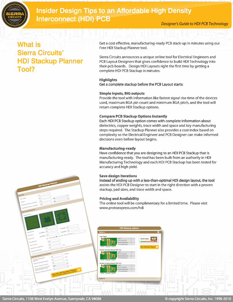
What is Sierra Circuits’ HDI Stackup Planner Tool?
Get a cost effective, manufacturing-ready PCB stack-up in minutes using our Free HDI Stackup Planner tool.
Sierra Circuits announces a unique online tool for Electrical Engineers and PCB Layout Designers that gives confidence to build HDI Technology into their pcb boards. Design HDI Layouts right the first time by getting a complete HDI PCB Stackup in minutes.
Highlights Get a complete stackup before the PCB Layout starts:Get a complete stackup before the PCB Layout starts:
Simple inputs, BIG outputsProvide the tool with information like fastest signal rise time of the devices used, maximum BGA pin count and minimum BGA pitch, and the tool will return complete HDI Stackup options.
Compare PCB Stackup Options InstantlyEach HDI PCB Stackup option comes with complete information about Each HDI PCB Stackup option comes with complete information about dielectrics, copper weights, trace width and space and key manufacturing steps required. The Stackup Planner also provides a cost index based on complexity so the Electrical Engineer and PCB Designer can make informed decisions even before layout begins.
Manufacturing-readyHave confidence that you are designing to an HDI PCB Stackup that is Have confidence that you are designing to an HDI PCB Stackup that is manufacturing-ready. The tool has been built from an authority in HDI Manufacturing Technology and each HDI PCB Stackup has been tested for accuracy and high yield.
Save design iterationsInstead of ending up with a less-than-optimal HDI design layout, the tool Instead of ending up with a less-than-optimal HDI design layout, the tool assists the HDI PCB Designer to start in the right direction with a proven stackup, pad sizes, and trace width and space.
Pricing and AvailabilityThe online tool will be complimentary for a limited time. Please visit www.protoexpress.com/hdi

Insider Design Tips to an Affordable High Density Interconnect (HDI) PCB
Designer’s Guide to HDI PCB Technology
Sierra Circuits, 1108 West Evelyn Avenue, Sunnyvale, CA 94086 © copyright Sierra Circuits, Inc. 1998-2010
Choose the right PCB Material
Material selection is, of course, important for all PCB designs. It is especially important for HDI PCB manufacturing because there are additional manufacturing constraints that play a role. Proper material selection is also important for layout design since materials will affect the electrical performance of the signal traces. The physical thickness of the material is important when considering the aspect ratio of the micro-via to be plated. The current standard aspect ratio for a micro via is 0.75:1. (The micro-via diameter should be larger than the height of the material it is penetrating to the next adjacent layer.)
A
b
c
(Top View)
(Cross section view)
b
d
a
DESIGN LAYOUT GUIDELINES
Insider Design Tips to an Affordable High Density Interconnect (HDI) PCB
Designer’s Guide to HDI PCB Technology
Sierra Circuits, 1108 West Evelyn Avenue, Sunnyvale, CA 94086 © copyright Sierra Circuits, Inc. 1998-2010
Choose the right PCB Material
Other material considerations are the maximum withstanding temperature, maximum frequency of signals and coefficients of thermal expansion (CTE). The maximum temperature here refers to that temperature which the PCB is required to withstand without affecting its mechanical integrity. It is usually expressed in degrees Celsius. Maximum frequency refers to the highest frequency that the electrical signals realized on the PCB are operating at. This is usually expressed in MHz or GHz. Our Engineering Staff will ask you the fastest rise time during circuit operation and help narrow down the selection of material that would meet your requirements.
AlongAlong with these items, the dielectric constant of the material and the dielectric loss or dissipation factor will also play vital roles in material selection.
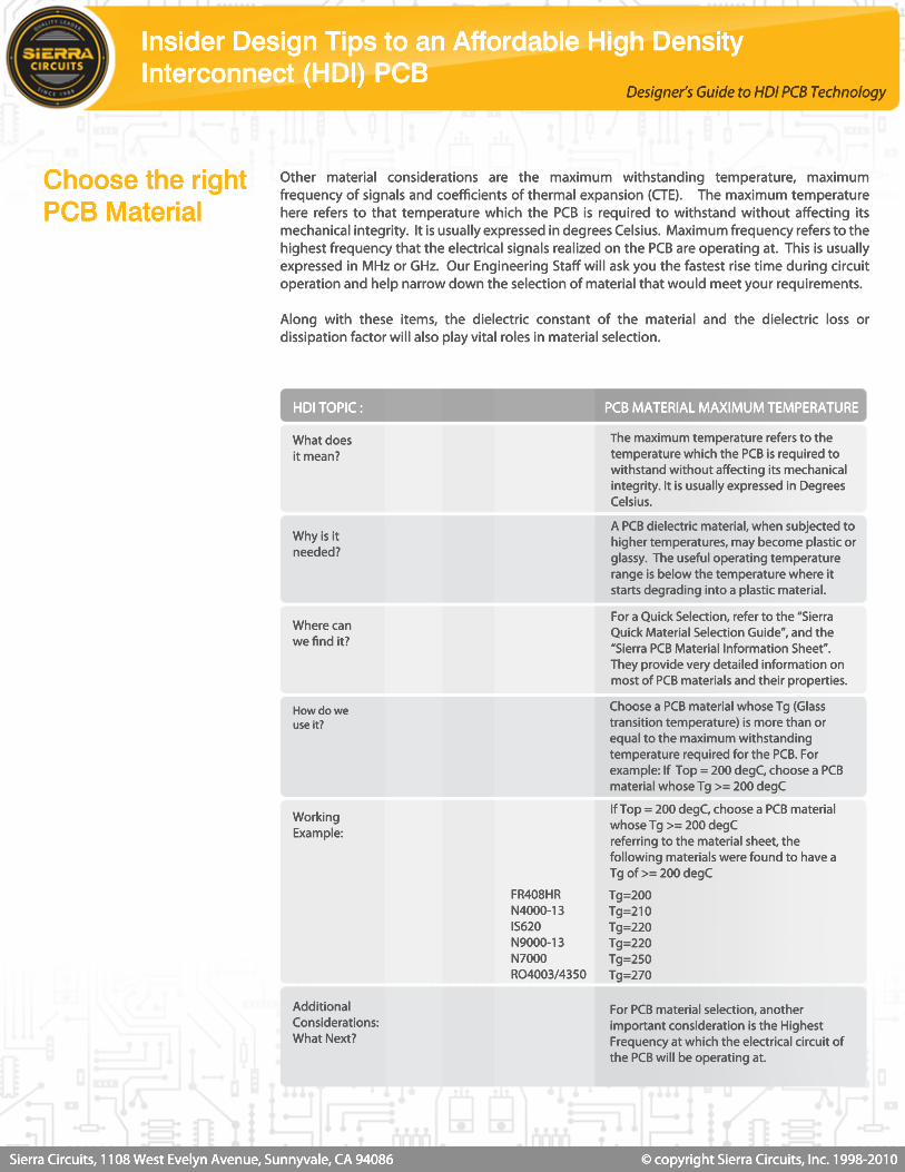
HDI TOPIC : PCB MATERIAL MAXIMUM TEMPERATURE
What does it mean?
The maximum temperature refers to the temperature which the PCB is required to withstand without affecting its mechanical integrity. It is usually expressed in Degrees Celsius.
Why is it needed?
A PCB dielectric material, when subjected to higher temperatures, may become plastic or glassy. The useful operating temperature range is below the temperature where it starts degrading into a plastic material.
Where can we find it?
For a Quick Selection, refer to the “Sierra Quick Material Selection Guide”, and the “Sierra PCB Material Information Sheet”. They provide very detailed information on most of PCB materials and their properties.
How do we use it?
Choose a PCB material whose Tg (Glass transition temperature) is more than or equal to the maximum withstanding temperature required for the PCB. For example: If Top = 200 degC, choose a PCB material whose Tg >= 200 degC
Working Example:
FR408HRN4000-13IS620N9000-13N7000RO4003/4350
Tg=200Tg=210Tg=220Tg=220Tg=250Tg=270
If Top = 200 degC, choose a PCB material whose Tg >= 200 degCreferring to the material sheet, the following materials were found to have a Tg of >= 200 degC
Additional Considerations: What Next?
For PCB material selection, another important consideration is the Highest Frequency at which the electrical circuit of the PCB will be operating at.

Insider Design Tips to an Affordable High Density Interconnect (HDI) PCB
Designer’s Guide to HDI PCB Technology
Sierra Circuits, 1108 West Evelyn Avenue, Sunnyvale, CA 94086 © copyright Sierra Circuits, Inc. 1998-2010
Have a plan for your PCB Stack-up and Micro Via Structures
The total number of layers of your final HDI PCB is determined by BGA (or the highest pin count device), signals break-out, the number of signal layers, as well as the number of power and ground layers. The number of power and ground layers can be determined by taking into account the number of grounds, the number of different major voltages in the circuit, as well as signal integrity/control impedance requirements.
TheThe sequence in which the layers are put together (signal, power, ground, etc) is another factor that affects signal performance and allows for a balanced PCB structure. It is always good practice to order the layers in a balanced manner. You should have the number of plane and signal layers both ODD or both EVEN (both EVEN is the best for a balanced structure). They should also be symmetrically placed.
MicroMicro Via Structures can also have a big impact on the manufacturing process, since they directly affect the number of lamination cycles. The more variations you have of which layers micro-via start and stop on, the more number of lamination steps are needed by the PCB manufacturing. Which layers the micro via starts and stops on creates a sub-construction, and each sub-construction will require an extra lamination cycle. (The lamination process is defined as pressing a set of copper layers with dielectrics in between two adjacent copper layers under heat and pressure to form a multilayer PCB laminate).
Getting design help from the PCB Manufacturer: Too much of a good thing?Getting design help from the PCB Manufacturer: Too much of a good thing?
Leaning on your PCB fabricator too much has its pros and cons.
MostMost PCB fabricators have fleshed out their engineering support to be able to provide basic feedback on your HDI PCB layout. This is great information, but only up to a certain level. A PCB fabricator will seldom take into account your decision-making criteria when looking at your circuit schematics or BOM. If you want a strict review of your layout, there is no need to waste your time waiting for a response from the PCB fabricator’s engineer. There are online web tools available that will provide this service quickly and with great detail. (Freedfm.com and BetterDFM.com)
A new design tool from Sierra Circuits to get HDI designers plan it right!
AtAt Sierra Circuits, our engineering staff has been trained on the topics discussed in this article and can analyze the design from a holistic point of view. Their analysis starts with determining the density of the most demanding component. Then, through a systematic set of questions and answers using our in-house HDI Assistance design tool, we can recommend a set of stack-up recommendations that meet your cost, performance and timeline needs.
ConclusionInIn this paper we have outlined key decisions required for a planned approach to HDI Design. We hope it provides you with a deeper understanding of the HDI Design Process as well as important tricks and tips to make HDI work for you!
Insider Design Tips to an Affordable High Density Interconnect (HDI) PCB
Designer’s Guide to HDI PCB Technology
Sierra Circuits, 1108 West Evelyn Avenue, Sunnyvale, CA 94086 © copyright Sierra Circuits, Inc. 1998-2010
About Sierra Circuits
Sierra Circuits is a US based manufacturer of High Density Interconnect PCBs (HDI PCBS). Our specialty is quick turn, high technology and small to medium production of printed circuit boards. Our capabilities include laser micro vias, blind and burried vias, fine lines and spaces, sequential lamination, via-in-pad technology. With our in-house YAG laser machines, we can laser drill 2 mil, or 50 micron, size micro vias. Sierra Circuits has also pioneered fine line capability. With our laser direct imaging systems, we can provide consistent traces and spaces down to 35 microns in diameter. We also specialize in sequential build applications, using typical PCB materials like FR4, Polyimide,Polyimide, and RCC. We can provide up to 4 build-up layers on expedited lead times. Typical micro via structures include stacked microvias, buried microvias, staggered or stepped microvias.
For our microelectronics pcbs and pcb substrates, we can provide build-up technology with fine lines and spaces down to 40 microns, high temperature materials, like polyimide, stacked micro vias, buried resistors, and multi-tiered cavity pcbs. We have provided microelectronic pcbs with fine pitch devices down to 200 microns, using 50 micron lase drilled via-in-pad technology and thin build-up materials. Our quality checks include surface cleanliness and wire bondability. Some examples of surface finish include OSP, ENIG, ENEPIG, Soft Gold.
OurOur Engineering support provides valuable suggestions with their knowledge of high speed designs, analog/digital, high density pcb manufacturing design rules and design for assembly rules. Upload your data and receive a free consultation and review of your design. Services include system level design, schematic capture, pcb layout, and pcb/pcba DFM.