IEEE TRANSACTIONS ON MICROWAVE THEORY AND...
7
IEEE TRANSACTIONS ON MICROWAVE THEORY AND TECHNIQUES, VOL. 55, NO. 9, SEPTEMBER 2007 1919 Air-Gap Transmission Lines on Organic Substrates for Low-Loss Interconnects Todd J. Spencer, Student Member, IEEE, Paul Jayachandran Joseph, Tae Hong Kim, Student Member, IEEE, Madhavan Swaminathan, Fellow, IEEE, and Paul A. Kohl, Member, IEEE Abstract—The fabrication of low-loss transmission line struc- tures with an air dielectric layer is described. The channels are characterized at low frequency (10 and 100 kHz) using capaci- tance and loss tangent and at high frequency (500 MHz to 10 GHz) using -parameter measurements. The incorporation of an air gap resulted in structures with effective dielectric constants between 1.5–1.8 and significantly lower loss tangents. The fabrication tech- nique could be used to create more complicated air gap transmis- sion line structures for use in monolithic microwave integrated cir- cuits. Index Terms—Air gaps, dielectric losses, multiprocessor inter- connection, transmission lines. I. INTRODUCTION F UTURE generations of high-performance microproces- sors require cost-effective manufacturable packages and substrates, which lower the dielectric permittivity, provide a spatially uniform electrical environment, and which address global wiring scaling issues [1]. One area of particular interest is the propagation of high-frequency signals through transmission lines without sacrificing circuit performance. This is especially important for multichip modules and high-performance servers, routers, and switches where interchip distances can be large and signal strength may be significantly degraded. A variety of material processing and signal-processing techniques are currently being pursued to achieve low-loss transmission lines for these applications. Conventional substrates used in monolithic microwave inte- grated circuits (MMICs), such as GaAs, or other high-perfor- mance substrates, such as Duroid, offer good loss character- istics, but are expensive relative to the much lower cost fiber- glass/epoxy substrates based on resins of tetra-bromo bisphenol A (FR-4) and bismaleimide triazine (BT). While FR-4 is attrac- tive for its low cost, it has a relatively high loss characteristic, Manuscript received November 7, 2006; revised February 19, 2007. This work was supported by the Defense Advanced Research Projects Agency (DARPA)/Microelectronics Advanced Research Corporation (MARCO) In- terconnect Focus Center. This work was supported in part by MARCO, its participating companies, and DARPA under Contract 2003-IT-674. T. J. Spencer, P. J. Joseph, and P. A. Kohl are with the School of Chemical and Biomolecular Engineering, Georgia Institute of Technology, Atlanta, GA 30318 USA (e-mail: [email protected]). T. H. Kim and M. Swaminathan are with the School of Electrical and Com- puter Engineering, Georgia Institute of Technology, Atlanta, GA 30318 USA. Color versions of one or more of the figures in this paper are available online at http://ieeexplore.ieee.org. Digital Object Identifier 10.1109/TMTT.2007.904326 which results in significant power dissipation in the dielectric. Typical FR-4 materials have dielectric constants in the range of 4.2–5.5 and a loss tangent of approximately 0.02. At high fre- quencies, the dielectric loss becomes the dominant loss mecha- nism [2]. Substrate integrated waveguides on FR-4 optimized for low loss, low crosstalk, and maximum bandwidth were reported in [3]. Such waveguide structures achieved low-loss without multimoding and were shown to be compatible with current manufacturing technologies. However, the dimensions are large (linewidths greater than 2.8 mm) and cannot be easily scaled for integration with multichip modules. Digital signal-processing techniques, which can improve data rates, are also being aggressively pursued as an alternative to passive solutions using low-loss materials. These techniques include four-layer pulse amplitude modulation (PAM-4) and duobinary signaling. However, they can increase the circuit complexity and may result in increased power consumption [4]. Previous work by Kohl et al. has presented techniques for air cavity encapsulation using an SiO encapsulant deposited by plasma enhanced chemical vapor deposition and a thermally decomposed sacrificial polymer [5]. The gaseous products from the decomposition reaction are able to permeate through the overcoat leaving an air gap with little residue. Similar encapsu- lation techniques using sacrificial polymers were demonstrated using Avatrel as the encapsulant material. A variety of sizes and aspect ratios were reported [6]. Fabrication of two-layer stacked air gaps was also demonstrated [7]. Work by Jayachandran et al. demonstrated air cavity forma- tion in Avatrel with reduced decomposition temperature with the addition of small quantities of photoacid generator [8]. The acid catalyzed reaction mechanism was described and the pri- mary products of the decomposition were shown to be acetone and carbon dioxide. The photo acid generator salts lower both the thermal and photolytic decomposition temperature via an acid-catalyzed decomposition reaction. The lower decomposi- tion temperature has several benefits, including reduced energy needs and compatibility with organic substrates. Presented in this study for the first time is a novel fabrication process and measured results for low-loss transmission lines with air cladding. The transmission line structures were fabri- cated in parallel-plate and suspended ground microstrip config- urations on FR-4 and BT substrates. The processing techniques are compatible with conventional MMIC fabrication. The air- gapped structure significantly lowers both the effective dielec- tric constant and dissipation factor, resulting in lower attenua- tion and phase loss in the line. 0018-9480/$25.00 © 2007 IEEE
-
Upload
nguyenkhanh -
Category
Documents
-
view
223 -
download
1
Transcript of IEEE TRANSACTIONS ON MICROWAVE THEORY AND...
IEEE TRANSACTIONS ON MICROWAVE THEORY AND TECHNIQUES, VOL. 55, NO. 9, SEPTEMBER 2007 1919
Air-Gap Transmission Lines on OrganicSubstrates for Low-Loss Interconnects
Todd J. Spencer, Student Member, IEEE, Paul Jayachandran Joseph, Tae Hong Kim, Student Member, IEEE,Madhavan Swaminathan, Fellow, IEEE, and Paul A. Kohl, Member, IEEE
Abstract—The fabrication of low-loss transmission line struc-tures with an air dielectric layer is described. The channels arecharacterized at low frequency (10 and 100 kHz) using capaci-tance and loss tangent and at high frequency (500 MHz to 10 GHz)using -parameter measurements. The incorporation of an air gapresulted in structures with effective dielectric constants between1.5–1.8 and significantly lower loss tangents. The fabrication tech-nique could be used to create more complicated air gap transmis-sion line structures for use in monolithic microwave integrated cir-cuits.
Index Terms—Air gaps, dielectric losses, multiprocessor inter-connection, transmission lines.
I. INTRODUCTION
FUTURE generations of high-performance microproces-sors require cost-effective manufacturable packages and
substrates, which lower the dielectric permittivity, provide aspatially uniform electrical environment, and which addressglobal wiring scaling issues [1]. One area of particular interest isthe propagation of high-frequency signals through transmissionlines without sacrificing circuit performance. This is especiallyimportant for multichip modules and high-performance servers,routers, and switches where interchip distances can be largeand signal strength may be significantly degraded. A varietyof material processing and signal-processing techniques arecurrently being pursued to achieve low-loss transmission linesfor these applications.
Conventional substrates used in monolithic microwave inte-grated circuits (MMICs), such as GaAs, or other high-perfor-mance substrates, such as Duroid, offer good loss character-istics, but are expensive relative to the much lower cost fiber-glass/epoxy substrates based on resins of tetra-bromo bisphenolA (FR-4) and bismaleimide triazine (BT). While FR-4 is attrac-tive for its low cost, it has a relatively high loss characteristic,
Manuscript received November 7, 2006; revised February 19, 2007. Thiswork was supported by the Defense Advanced Research Projects Agency(DARPA)/Microelectronics Advanced Research Corporation (MARCO) In-terconnect Focus Center. This work was supported in part by MARCO, itsparticipating companies, and DARPA under Contract 2003-IT-674.
T. J. Spencer, P. J. Joseph, and P. A. Kohl are with the School of Chemicaland Biomolecular Engineering, Georgia Institute of Technology, Atlanta, GA30318 USA (e-mail: [email protected]).
T. H. Kim and M. Swaminathan are with the School of Electrical and Com-puter Engineering, Georgia Institute of Technology, Atlanta, GA 30318 USA.
Color versions of one or more of the figures in this paper are available onlineat http://ieeexplore.ieee.org.
Digital Object Identifier 10.1109/TMTT.2007.904326
which results in significant power dissipation in the dielectric.Typical FR-4 materials have dielectric constants in the range of4.2–5.5 and a loss tangent of approximately 0.02. At high fre-quencies, the dielectric loss becomes the dominant loss mecha-nism [2].
Substrate integrated waveguides on FR-4 optimized for lowloss, low crosstalk, and maximum bandwidth were reportedin [3]. Such waveguide structures achieved low-loss withoutmultimoding and were shown to be compatible with currentmanufacturing technologies. However, the dimensions are large(linewidths greater than 2.8 mm) and cannot be easily scaledfor integration with multichip modules.
Digital signal-processing techniques, which can improvedata rates, are also being aggressively pursued as an alternativeto passive solutions using low-loss materials. These techniquesinclude four-layer pulse amplitude modulation (PAM-4) andduobinary signaling. However, they can increase the circuitcomplexity and may result in increased power consumption [4].
Previous work by Kohl et al. has presented techniques forair cavity encapsulation using an SiO encapsulant depositedby plasma enhanced chemical vapor deposition and a thermallydecomposed sacrificial polymer [5]. The gaseous products fromthe decomposition reaction are able to permeate through theovercoat leaving an air gap with little residue. Similar encapsu-lation techniques using sacrificial polymers were demonstratedusing Avatrel as the encapsulant material. A variety of sizes andaspect ratios were reported [6]. Fabrication of two-layer stackedair gaps was also demonstrated [7].
Work by Jayachandran et al. demonstrated air cavity forma-tion in Avatrel with reduced decomposition temperature withthe addition of small quantities of photoacid generator [8]. Theacid catalyzed reaction mechanism was described and the pri-mary products of the decomposition were shown to be acetoneand carbon dioxide. The photo acid generator salts lower boththe thermal and photolytic decomposition temperature via anacid-catalyzed decomposition reaction. The lower decomposi-tion temperature has several benefits, including reduced energyneeds and compatibility with organic substrates.
Presented in this study for the first time is a novel fabricationprocess and measured results for low-loss transmission lineswith air cladding. The transmission line structures were fabri-cated in parallel-plate and suspended ground microstrip config-urations on FR-4 and BT substrates. The processing techniquesare compatible with conventional MMIC fabrication. The air-gapped structure significantly lowers both the effective dielec-tric constant and dissipation factor, resulting in lower attenua-tion and phase loss in the line.
0018-9480/$25.00 © 2007 IEEE
1920 IEEE TRANSACTIONS ON MICROWAVE THEORY AND TECHNIQUES, VOL. 55, NO. 9, SEPTEMBER 2007
II. BACKGROUND
The wave propagation factor of an exponentially decayingelectromagnetic wave propagating in the -direction can beexpressed in terms of its real and imaginary parts as
(1)
where is the attenuation constant and is the phase constant.Expressed in terms of the phase constant, the wave propagationvelocity is given as
(2)
where is the angular frequency, is the speed of light invacuo, and is the relative permittivity of the dielectric. Thus,increased propagation velocity and reduced phase loss areachieved in materials with low dielectric constants [9], [10].
The real component of the wave damping factor in a trans-mission line consists of loss contributions from the conductorand dielectric. The conductor loss in a parallel-plate waveguidecan be expressed as follows:
(3)
where is the free-space permeability, is the relative per-meability, is the conductivity, is the intrinsic impedance offree space (377 ), and is the distance between conductors.The dielectric loss can be expressed by
(4)
where is the loss tangent, or dissipation factor, of themedium [9]. From (4) and (5), it can be seen that the conductorloss scales with the square root of frequency, while the dielec-tric loss scales linearly with the frequency. Similar expressionsfor the conductor and dielectric losses in a microstrip were ex-pressed by Hammerstad et al. using an effective dielectric con-stant [11]. The dielectric loss in a microstrip line is somewhatlower than in a parallel-plate line, but is still usually the dom-inant loss mechanism at high frequencies. It is clear from (3)and (4) that reduction of the dielectric constant reduces the lossin both mechanisms. Transmission line structures using higherconductivity materials will have lower conductor losses, whiledielectric materials with lower loss tangents diminish the con-tribution of the dielectric.
In order to increase signal propagation velocity and reducedielectric loss in a transmission line, an air gap can be includedin the dielectric layer to lower its relative permittivity [9]. Thedielectric constant of an air-gapped substrate can be calculatedfrom
(5)
where is the relative permittivity of the substrate and andare the thicknesses of the substrate and air gap, respectively
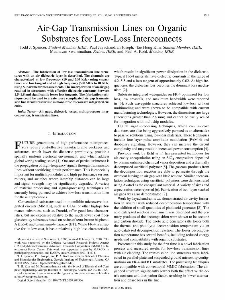
Fig. 1. Simplified process flow diagram.
[12]. The effective dielectric of such an air-gapped structure ap-proaches unity when the substrate thickness is minimized.
Air-gap transmission lines using a dielectric post for struc-tural support were demonstrated by Jeong et al. on GaAssubstrates [13]. Devices were fabricated in several conventionaltransmission line geometries using both surface microma-chining and photolithography [14], [15]. Microstrip antennadesigns on Duroid and FR-4 substrates have also utilized airgaps to achieve lower dielectric constants. The incorporation ofan air insulation layer reduces the substrate loss characteristic[16]–[18].
Many different techniques to create air gaps have been in-vestigated for use in microelectronics, including oxidation ofsputtered carbon [19], oxidation of photoresist and other organicmaterials [5], thermal decomposition of sacrificial polymers [7],reflow of photoresist [13], and dissolution of photoresist intoa solvent [14]. The former methods require high temperatures( C), which are incompatible with organic substrateprocessing, while the latter require a fluid path to allow for con-tact of the photoresist with solvent.
III. FABRICATION PROCESS
Air-insulated parallel-plate and suspended ground microstriplines were created on organic substrates using CMOS-compat-ible processing techniques and sacrificial polymer with a pho-toacid generator. A copper signal line was etched with a sacri-ficial polymer layer defined around it. The polymer is then cov-ered with an overcoat and an electroplated ground line
Illustrated in Fig. 1 is a simplified process flow diagram of thebuildup procedure used in the fabrication. The substrate usedwas an FR-4 or BT substrate clad with 27- m-thick copper.AZ4620 photoresist from Clariant, Somerville, NJ, was spun toa thickness of 10 m onto the substrate and soft baked at 110 Cfor 10 min. The resist was photopatterned and developed to de-fine the 220- m-wide transmission lines. The exposed copperwas etched with a solution of 15% H O and 5% H SO . Thephotoresist was then stripped, leaving only the signal lines onthe board shown in Fig. 1(a). The signal lines were 58 mm inlength.

SPENCER et al.: AIR-GAP TRANSMISSION LINES ON ORGANIC SUBSTRATES FOR LOW-LOSS INTERCONNECTS 1921
Fig. 2. Dimensions for electrostatic and high-frequency simulations. The di-mensions for the parallel-plate structures are a = 24 �m, b = 20 �m, c =
15 �m, d = 27 �m, e = 1 �m, f = 220�m, g = 220�m, and h = 600�m.For the narrow ground line case, dimensions are the same, except f = 150�m.For the suspended ground microstrip, dimensions are the same, except c =
30 �m and f = 650 �m.
The photosensitive sacrificial polymer, Unity 2203P fromPromerus LLC, Brecksville, OH, was spun onto the board to athickness of 15 m. Following a 10–min soft bake, the Unitywas photodefined, developed on a hot plate at 110 C for 10 min,and rinsed with isopropyl alcohol leaving 600- m-wide encap-sulation regions over the signal lines, as shown in Fig. 1(b).
Avatrel 2000P dielectric polymer from Promerus LLC wasspun onto the board at a thickness of 20 m over the encapsu-lated copper lines, as illustrated in Fig. 1(c). The Avatrel wasthen dosed with 200 mJ cm ( nm) and developed todefine regions allowing access to the probe pads. An electro-plating seed layer of Ti/Cu/Ti was sputtered onto the Avatrelovercoat at thicknesses of 150 Å/1000 Å/150 Å, respectively.The titanium layers are required for adhesion of the copper tothe overcoat polymer and the photoresist.
AZ4620 photoresist was again spun to a thickness of 10 mand exposed to define an electroplating mask for ground linesof three different widths (150, 220, and 650 m). The titaniumlayer was removed with a buffered oxide etch solution. Thecopper ground lines were electroplated to a thickness of 20 mand the photoresist was stripped. The sputtered layer of titaniumwas etched away with BOE, the copper was etched away witha solution of 7.5% H O and 5% H SO , and the final layer oftitanium was etched with BOE. This etched line structure, in-cluding the titanium adhesion layer between the ground copperand the overcoat polymer, is shown in Fig. 1(d).
The polymer overcoat was then cured in a nitrogen purgedtube furnace heated to 180 C for 2 h at a ramp rate of 3 C minfrom 25 C to 150 C and 1 C min from 150 C to 180 C. TheAvatrel cured while the decomposition products of the encapsu-lated Unity permeated through the overcoat, leaving the struc-ture pictured in Fig. 1(e). The structure dimensions are shownin Fig. 2.
A scanning electron microscope (SEM) cross section of thefabricated parallel-plate line is shown in Fig. 3. A line with anarrow ground line (150- m wide) is shown in Fig. 4. Slightresidue from the sacrificial polymer is visible in the corner of thecavity, but is not expected to impact performance. A top view ofthe probe pads for the parallel-plate structure is shown in Fig. 5.
IV. CAPACITANCE AND LOSS TANGENT REDUCTION
The structures were characterized at low frequency using anHP4263A LCR meter to measure capacitance and loss tangent
Fig. 3. SEM of the parallel-plate line. The ground line is slightly peeled backdue to delamination during the dicing process. The particle in the air gap is alsoa result of the dicing process.
Fig. 4. SEM of the narrow width ground line. The 150-�m-wide ground lineis peeled back due to delamination during the dicing process. Slight residue isseen in the right corner of the air cavity, but is not expected to impact electricalperformance.
at 10 and 100 kHz. Measurements were taken before and afterdecomposition of the sacrificial polymer. The capacitance of thestructures was simulated using a 2-D electrostatic field simu-lator. The material properties used in the simulation are listedin Table I.
The LCR meter was calibrated according to the manufac-turer’s instructions by performing open, short, and cable cor-rections. Probe needles were first separated by several centime-ters to perform the open correction and then touched together toperform the short correction. The LCR meter also enabled ac-counting for effects of the 1-m cables. The structures were thenprobed from one end by first lowering one probe needle ontothe ground probe pad and then lowering the other onto the padfor the signal line. No change in measured results was observedwhen the probe needle positions were reversed. For capacitancemeasurements, the LCR meter has an error of 0.1 pF.

1922 IEEE TRANSACTIONS ON MICROWAVE THEORY AND TECHNIQUES, VOL. 55, NO. 9, SEPTEMBER 2007
Fig. 5. Top view of parallel-plate structure probe pads.
TABLE IMATERIAL PROPERTIES USED IN SIMULATIONS
Summarized in Table II are the measured values of capaci-tance before and after decomposition of the sacrificial polymer.The formation of the air gap resulted in a reduction of capaci-tance of 27%–44% at 10 kHz. Results at 100 kHz were slightlyless capacitive (measurements were between 0.–0.2 pF lowerthan 10 kHz). The capacitance reduction is consistent with thereduction in effective dielectric expected from (5). The simu-lated values of capacitance are somewhat higher than measuredresults, although air-gap inclusion results in a similar capaci-tance reduction. Better agreement between simulated and mea-sured result is possible by accounting for topographical features.Simulated capacitance does not include probe pad effects andtreats the line as having uniform dimensions along the 58-mmline. An air-gap parallel-plate structure has a capacitance 39%lower than an equivalent thickness of Avatrel (which has a ca-pacitance of 9.69 pF) and 60% lower than an equivalent thick-ness of FR-4 (which has a capacitance of 14.77 pF).
The variance observed in the measured capacitance resultsfor similar lines are likely due to processing defects. Edge ef-fects were particularly important for the 650- m-wide groundline due to the inability to process larger board sizes. The threemeasured lines with 150- m-wide ground planes have very littlevariance between them. It is expected that in a manufacturingenvironment, this variance could be further reduced.
TABLE IICAPACITANCE MEASUREMENTS BEFORE AND AFTER UNITY DECOMPOSITION
TABLE IIILOSS TANGENT MEASUREMENTS BEFORE AND AFTER UNITY DECOMPOSITION
The measured values of the loss tangent for these structuresare shown in Table III. The loss tangent was read directly fromthe LCR meter simultaneously with the capacitance measure-ment. The inclusion of the air gap significantly reduced the dis-sipation factor of the lines. A loss tangent reduction of greaterthan 85% was observed for each of the structures. The reducedcapacitance and loss tangent values verify the presence of theair gap.
V. HIGH-FREQUENCY CHARACTERISTICS
The parallel-plate structure was characterized at highfrequency using an Agilent 8720ES -parameter network ana-lyzer. The scattering parameters were measured from 100 MHzto 10 GHz using ground–signal–ground (GSG) probes with apitch of 150 m. Simulation of the high-frequency performanceof these structures was performed using the High FrequencyStructure Simulator (HFSS) by Ansoft.
Prior to measurement, the network analyzer and probes werecalibrated using a short, open, load, thru (SOLT) calibration.
SPENCER et al.: AIR-GAP TRANSMISSION LINES ON ORGANIC SUBSTRATES FOR LOW-LOSS INTERCONNECTS 1923
(a)
(b)
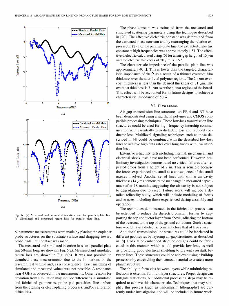
Fig. 6. (a) Measured and simulated insertion loss for parallel-plate line.(b) Simulated and measured return loss for parallel-plate line.
-parameter measurements were made by placing the coplanarprobe structures on the substrate surface and dragging towardprobe pads until contact was made.
The measured and simulated insertion loss for a parallel-plateline 58-mm long are shown in Fig. 6(a). Measured and simulatedreturn loss are shown in Fig. 6(b). It was not possible todeembed these measurements due to the limitations of theresearch test vehicle and, as a consequence, exact matching ofsimulated and measured values was not possible. A resonancenear 4 GHz is observed in the measurements. Other reasons fordeviation from simulation may include differences in simulatedand fabricated geometries, probe pad parasitics, line defectsfrom the etching or electroplating processes, and/or calibrationdifficulties.
The phase constant was estimated from the measured andsimulated scattering parameters using the technique describedin [20]. The effective dielectric constant was determined fromthe extracted phase constant and by rearranging the relation ex-pressed in (2). For the parallel-plate line, the extracted dielectricconstant at high frequencies was approximately 1.51. The effec-tive dielectric calculated using (5) for an air-gap height of 15 mand a dielectric thickness of 20 m is 1.52.
The characteristic impedance of the parallel-plate line wasapproximately 40 . This is lower than the targeted character-istic impedance of 50 as a result of a thinner overcoat filmthickness over the sacrificial polymer regions. The 20- m over-coat thickness is less than the desired thickness of 31 m. Theovercoat thickness is 31 m over the planar regions of the board.This effect will be accounted for in future designs to achieve acharacteristic impedance of 50 .
VI. CONCLUSION
Air-gap transmission line structures on FR-4 and BT havebeen demonstrated using a sacrificial polymer and CMOS com-patible processing techniques. These low-loss transmission linestructures could be used for high-frequency interchip commu-nication with essentially zero dielectric loss and reduced con-ductor loss. Multilevel signaling techniques such as those de-scribed in [4] could be combined with the described low-losslines to achieve high data rates over long traces with low inser-tion loss.
Extensive reliability tests including thermal, mechanical, andelectrical shock tests have not been performed. However, pre-liminary investigation demonstrated no critical failures after re-peated drops from a height of 2 m. This is sensible becausethe forces experienced are small as a consequence of the smallmasses involved. Another set of lines with similar air cavitythickness (14 m) demonstrated no change in measured capaci-tance after 18 months, suggesting the air cavity is not subjectto degradation due to creep. Future work will include a de-tailed reliability study, which will include modeling of forcesand stresses, including those experienced during assembly andoperation.
The techniques demonstrated in the fabrication process canbe extended to reduce the dielectric constant further by sup-porting the top conductor layer from above, adhering the bottomof the overcoat to the top of the ground conductor. Such a struc-ture would have a dielectric constant close that of free space.
Additional transmission line structures could be fabricated indifferent geometries by layering air-gap structures, as describedin [8]. Coaxial or embedded stripline designs could be fabri-cated in this manner, which would provide low loss, as wellas providing good electrical shielding to prevent crosstalk be-tween lines. These structures could be achieved using a buildupprocess or by entrenching the overcoat material to create a moreplanar structure.
The ability to form vias between layers while minimizing re-flections is essential for multilayer structures. Proper design canmitigate reflections, but additional processing steps may be re-quired to achieve this characteristic. Techniques that may sim-plify this process (such as nanoimprint lithography) are cur-rently under investigation and will be included in future work.
1924 IEEE TRANSACTIONS ON MICROWAVE THEORY AND TECHNIQUES, VOL. 55, NO. 9, SEPTEMBER 2007
An additional benefit of imprint lithography is the ability to de-fine smaller features in the sacrificial polymer.
Detailed investigation of electrical performance of differentstructure geometries including simulated eye diagrams will beincluded in a future study. Comparisons will be made betweenembedded stripline designs and parallel-plate and suspendedground microstrip lines. The electrical characteristics of vias,as well as coupling between lines will also be addressed.
ACKNOWLEDGMENT
This work was carried out as part of the Interconnect FocusCenter Research Program. The authors gratefully acknowledgethe technical support of the cleanroom staff of the Microelec-tronics Research Center, Georgia Institute of Technology, At-lanta.
REFERENCES
[1] International Technology Roadmap for Semiconductors, , Semicon-duct. Ind. Assoc., San Jose, CA, 2004.
[2] A. R. Djordjevic, R. M. Biljie, V. D. Likar-Smiljanic, and T. K. Sarkar,“Wideband frequency-domain characterization of FR-4 and time-do-main causality,” IEEE Trans. Electromagn. Compat., vol. 43, no. 4, pp.662–667, Nov. 2001.
[3] J. J. Simpson, A. Taflove, J. A. Mix, and H. Heck, “Substrate integratedwaveguides optimized for ultrahigh-speed digital interconnects,” IEEETrans. Microw. Theory Tech., vol. 54, no. 5, pp. 1983–1990, May 2006.
[4] J. Sinsky, M. Duelk, and A. Adamiecki, “High-speed electrical back-plane transmission using duobinary signaling,” IEEE Trans. Microw.Theory Tech., vol. 53, no. 1, pp. 152–160, Jan. 2005.
[5] P. A. Kohl et al., “Air-gaps for electrical interconnections,” Elec-trochem. Solid-State Lett., vol. 1, pp. 49–51, Jul. 1998.
[6] H. A. Reed, C. E. White, V. Rao, S. A. Bidstrup Allen, C. L. Henderson,and P. A. Kohl, “Fabrication of microchannels using polycarbonates assacrificial materials,” J. Micromech. Microeng., vol. 11, pp. 733–737,Nov. 2001.
[7] D. Bhusari, H. A. Reed, M. Wedlake, A. M. Padovani, S. A. BidstrupAllen, and P. A. Kohl, “Fabrication of air-channel structures for mi-crofluidic, microelectromechanical, and microelectronic applications,”J. Microelectromech. Syst., vol. 10, pp. 400–408, Sep. 2001.
[8] J. P. Jayachandran et al., “Air-channel fabrication for microelectrome-chanical systems via sacrificial photosensitive polycarbonates,” J. Mi-croelectromech. Syst., vol. 12, pp. 147–159, Apr. 2003.
[9] D. Pozar, Microwave Engineering, 3rd ed. New York: Wiley, 2004,pp. 98–105.
[10] A. F. A. Ayoub, “Analysis of rectangular microstrip antenna with airsubstrates,” J. Electromagn. Waves Applicat., vol. 17, pp. 1755–1766,Dec. 2003.
[11] I. J. Bahl and D. K. Trivedi, “A designer’s guide to microstrip line,”Microwaves, pp. 174–182, May 1977.
[12] K. F. Lee and J. S. Dahele, “Circular disc microstrip antenna with anairgap,” IEEE Trans. Antennas Propag., vol. AP-32, no. 8, pp. 880–884,Aug. 1984.
[13] I. Jeong et al., “High-performance air-gap transmission lines and in-ductors for millimeter wave applications,” IEEE Trans. Microw. TheoryTech., vol. 50, no. 12, pp. 2850–2855, Dec. 2002.
[14] H.-S. Lee et al., “New micromachined microstrip transmission lines forapplication in millimeter wave circuits,” Microw. Opt. Technol. Lett.,vol. 40, no. 1, pp. 6–9, Jan. 2004.
[15] H.-S. Lee et al., “Fabrication of new micromachined transmission linewith dielectric posts for millimeter-wave applications,” J. Micromech.Microeng., vol. 14, pp. 746–749, May 2004.
[16] M. B. Anand, M. Yamada, and H. Shibata, “Use of gas as low-k in-terlayer dielectric in LSI’s: Demonstration of feasibility,” IEEE Trans.Electron Devices, vol. 44, no. 11, pp. 1965–1971, Nov. 1997.
[17] C. K. Queck and L. E. Devis, “Improved design of microstrip air-bridges,” Int. J. RF Microw. Comput.-Aided Eng., vol. 13, pp. 246–255,May 2003.
[18] G. Debatosh and J. Y. Siddiqui, “Resonant frequency of equilateraltriangular microstrip antenna with and without air gap,” IEEE Trans.Antennas Propag., vol. 52, no. 7, pp. 2174–2177, Aug. 2004.
[19] R. H. Havemann and S.-P. Jeng, “Multilevel interconnect structure withair gaps formed between metal leads,” U.S. Patent 5 461 003, Oct. 24,1995.
[20] W. R. Eisenstadt and Y. Eo, “S-parameter-based IC interconnect trans-mission line characterization,” IEEE Trans. Compon., Hybrids, Manuf.Technol., vol. 15, no. 4, pp. 483–490, Aug. 1992.
Todd J. Spencer (S’06) received the B.S. degreein chemical engineering from the University ofPittsburgh, Pittsburgh, PA, in 2003, and is currentlyworking toward the Ph.D. degree in chemical andbiomolecular engineering at the Georgia Institute ofTechnology, Atlanta.
He has a patent pending. His current research inthe Interconnect Focus Center, Georgia Institute ofTechnology, includes low-temperature decompos-able polymers for advanced electrical packaging onorganic substrates, thermal management, high-fre-
quency chip-to-board interconnects, and nanoimprint lithography.Mr. spencer is a member of the American Institute of Chemical Engineers
(AIChE) and Tau Beta Pi. He was the corecipient of the 2005 InternationalInterconnect Technology Conference (IITC) Best Student Paper Award, whichdemonstrated chip-level microfluidic cooling using conventional integrated cir-cuit fabrication techniques.
Paul Jayachandran Joseph received the Ph.D de-gree in physical–organic chemistry from the Univer-sity of Madras, Chennai, India, in 1997.
From 1994 to 1997, he was a Council of Scientificand Industrial Research–Senior Research Fellowwith the Department of Physical Chemistry, Uni-versity of Madras, where he performed extensiveresearch in phase transfer catalysis. From 1997 to2000, he was a Visiting Scientist with the NationalScience Council of Taiwan. In 2001, he was aResearch Scientist with the School of Chemical and
Biomolecular Engineering, Georgia Institute of Technology, Atlanta. In 2005,he became a Faculty Research Scientist and Biomedical Engineering ResearchCoordinator with the Microelectronics Research Center, Georgia Institute ofTechnology. He is also a Director of Communications with the Nano@TechExecutive Board, GT-MiRC. He authored or coauthored approximately 46publications in journals and conference proceedings. His current researchinterests include nanobiotechnology, bio-microelectromechanical systems(bio-MEMS), and biosensor applications as diagnostics and detection systems.
Tae Hong Kim (S’04) received the B.E. degree inelectronic engineering from Pusan National Uni-versity, Pusan, Korea, in 2001, the M.E. degree inelectrical and computer engineering from the KoreaAdvanced Institute of Science and Technology(KAIST), Daejeon, Korea, in 2003, and is currentlyworking toward the Ph.D. degree in electrical andcomputer engineering at the Georgia Institute ofTechnology, Atlanta.
Since 2003, he has been a Graduate Research As-sistant with the Packaging Research Center (PRC),
Georgia Institute of Technology. He has authored or coauthored over 15 pub-lications in refereed journals and conferences. He has two patents pending.His research interests include signal integrity, power integrity, and high-speedpackage/mixed-signal system/interconnect design, modeling, test, and analysis.
Mr. Kim was the recipient of the Outstanding Poster Paper Award presentedat the 56th Electronic Components and Technology Conference (ECTC).

SPENCER et al.: AIR-GAP TRANSMISSION LINES ON ORGANIC SUBSTRATES FOR LOW-LOSS INTERCONNECTS 1925
Madhavan Swaminathan (A’91–M’95–SM’98–F’06) received the B.E. degree in electronics andcommunication from the University of Madras,Madras, India, in 1985, and the M.S. and Ph.D.degrees in electrical engineering from SyracuseUniversity, Syracuse, NY, in 1989 and 1991, respec-tively.
He is currently a Professor with the School of Elec-trical and Computer Engineering, Georgia Instituteof Technology, Atlanta, and the Deputy Director ofthe Packaging Research Center, Georgia Institute of
Technology. He founded and is the Chief Scientist of Jacket Micro Devices Inc.,Atlanta, GA, a company that specializes in integrated devices and modules forwireless applications. Prior to joining the Georgia Institute of Technology, hewas with the Advanced Packaging Laboratory, IBM, where he was involvedwith packaging for super computers. He has authored or coauthored over 250publications in refereed journals and conferences. He coauthored three bookchapters. He holds 11 patents with six pending.
Paul A. Kohl (A’92–M’03) received the Ph.D. degreein chemistry from The University of Texas at Austin,in 1978.
He is Regents’ Professor and HerculesInc./Thomas L. Gossage Chair of chemical en-gineering with the Georgia Institute of Technology,Atlanta. From 1978 to 1989, he was with AT&TBell Laboratories, where he was involved in newmaterials and processing methods for semiconductordevices. In 1989, he joined the faculty of the GeorgiaInstitute of Technology. His research interests
include ultra low-k dielectric materials, interconnects for microelectronicdevices, and electrochemical energy conversion devices. He is currently theDirector of the Interconnect Focus Center, Georgia Institute of Technology. Hehas authored or coauthored over 150 journal publications. He holds 40 patents.