1962 IEEE TRANSACTIONS ON MICROWAVE THEORY AND …
11
1962 IEEE TRANSACTIONS ON MICROWAVE THEORY AND TECHNIQUES, VOL. 56, NO. 8, AUGUST 2008 Modeling of Eye-Diagram Distortion and Data-Dependent Jitter in Meander Delay Lines on High-Speed Printed Circuit Boards (PCBs) Based on a Time-Domain Even-Mode and Odd-Mode Analysis Gawon Kim, Student Member, IEEE, Dong Gun Kam, Member, IEEE, Seung Jae Lee, Member, IEEE, Jaemin Kim, Student Member, IEEE, Myunghyun Ha, Student Member, IEEE, Kyoungchoul Koo, Student Member, IEEE, Jun So Pak, Member, IEEE, and Joungho Kim, Member, IEEE Abstract—Crosstalk induced in a meander delay line produces a significant amount of waveform distortion and data-dependent jitter at the output port. This paper introduces an interpretation of the eye-diagram distortion and the jitter generation mechanism based on a time-domain even- and odd-mode analysis of a cou- pled transmission line structure. From the proposed analysis, this paper proposes jitter-estimation equations for both the short and long unit line delay cases. The eye-diagram distortion and timing jitter are predicted and estimated, respectively. In order to verify the jitter-estimation equations, a series of microstrip-type printed circuit board test vehicles with the meander delay line are fabri- cated and tested. The measured jitter shows good agreement with the proposed jitter-estimation equations. Index Terms—Crosstalk, data-dependent jitter (DDJ), eye dia- gram, meander delay line. I. INTRODUCTION R ECENTLY, as clock frequencies and data transmission rates in semiconductor systems steadily increase over gi- gahertz frequency ranges, timing control of high-speed clock and digital data signal traces on printed circuit boards (PCBs) becomes a critical part of the PCB design task. A timing error of even a tiny fraction of the clock cycle time can cause serious timing problems between the clock trace and the signal traces or between the signal traces on the multilayer PCB. This ultimately limits are achievable clock frequency and data transmission rate of the system [1]. As a result, design methods for timing error minimization have attracted significant attention not only at chip and package design levels, but also at the PCB design level. As Manuscript received November 15, 2007; revised March 9, 2008. First pub- lished July 25, 2008; last published August 8, 2008 (projected). This work was supported by the Ministry of Knowledge Economy/Institute for Information Technology Advancement (MIC/IITA) under the Information Technology Re- search and Development Program (2005-S-118-02, Development of High-Per- formance and Smallest SiP Technology). G. Kim, J. Kim, K. Koo, J. S. Pak, and J. Kim are with the Department of Electrical Engineering, Korea Advanced Institute of Science and Technology (KAIST), Daejeon 305-701, Korea (e-mail: [email protected]). D. G. Kam is with High-Speed I/O Subsystems and Packaging, IBM T. J. Watson Research Center, Yorktown Heights, NY 10598 USA. S. J. Lee is with the Design Team, Research and Development Center, Amkor Technology Korea Inc., Seoul 133-706, Korea. M. Ha is with the Department of Electrical and Computer Engineering, Georgia Institute of Technology, Atlanta, GA 30332 USA. Digital Object Identifier 10.1109/TMTT.2008.927543 Fig. 1. Meander delay lines on PCB designs. (a) Meander delay line design on a mother board of a laptop computer. (b) Meander delay line designs on a mother board of a desktop computer. a method for reducing the timing error in the PCB design, delay lines have been adopted in critical nets to provide predetermined timing delay of the clock traces or the signal traces. A space and cost effective delay line structure should have a regular and delay-predictable shape with a compact design [2]. The most popular delay line scheme in PCB design is the meander-type structure, which consists of a group of unit delay lines with equal lengths, as shown in Fig. 1. The objective of the meander delay line is to achieve a precisely controlled timing delay of a clock or a signal trace with considerably enhanced surface area efficiency on the PCB [3]. However, since each unit delay line in the meander line struc- ture is facing its neighbor unit delay line so closely in a com- pact surface area, electromagnetic (EM) coupling crosstalk oc- curs between the adjacent lines. In particular, since the amount of the crosstalk at the delay line is heavily dependent on the data pattern and transmission rate, it can produce a considerable amount of the timing jitter at the high-speed digital data traces. This timing jitter is referred to as data-dependent jitter (DDJ) [4], [5]. As a consequence, predicting the eye-diagram distor- tion and estimating the timing-jitter increase caused by the EM coupling crosstalk in the meander delay line are considered as essential components of PCB design. There have been several attempts to analyze the EM coupling crosstalk effect at the meander delay line. Previous studies in [2], [3], [6]–[9] have pointed out that the crosstalk noise be- tween the unit delay lines at the meander delay line structure is accumulated synchronously at the receiving end due to inherent periodicity of the structure. In these studies, the crosstalk noise 0018-9480/$25.00 © 2008 IEEE
Transcript of 1962 IEEE TRANSACTIONS ON MICROWAVE THEORY AND …

1962 IEEE TRANSACTIONS ON MICROWAVE THEORY AND TECHNIQUES, VOL. 56, NO. 8, AUGUST 2008
Modeling of Eye-Diagram Distortion andData-Dependent Jitter in Meander Delay Lines on
High-Speed Printed Circuit Boards (PCBs) Based ona Time-Domain Even-Mode and Odd-Mode Analysis
Gawon Kim, Student Member, IEEE, Dong Gun Kam, Member, IEEE, Seung Jae Lee, Member, IEEE,Jaemin Kim, Student Member, IEEE, Myunghyun Ha, Student Member, IEEE,
Kyoungchoul Koo, Student Member, IEEE, Jun So Pak, Member, IEEE, and Joungho Kim, Member, IEEE
Abstract—Crosstalk induced in a meander delay line producesa significant amount of waveform distortion and data-dependentjitter at the output port. This paper introduces an interpretationof the eye-diagram distortion and the jitter generation mechanismbased on a time-domain even- and odd-mode analysis of a cou-pled transmission line structure. From the proposed analysis, thispaper proposes jitter-estimation equations for both the short andlong unit line delay cases. The eye-diagram distortion and timingjitter are predicted and estimated, respectively. In order to verifythe jitter-estimation equations, a series of microstrip-type printedcircuit board test vehicles with the meander delay line are fabri-cated and tested. The measured jitter shows good agreement withthe proposed jitter-estimation equations.
Index Terms—Crosstalk, data-dependent jitter (DDJ), eye dia-gram, meander delay line.
I. INTRODUCTION
R ECENTLY, as clock frequencies and data transmissionrates in semiconductor systems steadily increase over gi-
gahertz frequency ranges, timing control of high-speed clockand digital data signal traces on printed circuit boards (PCBs)becomes a critical part of the PCB design task. A timing errorof even a tiny fraction of the clock cycle time can cause serioustiming problems between the clock trace and the signal traces orbetween the signal traces on the multilayer PCB. This ultimatelylimits are achievable clock frequency and data transmission rateof the system [1]. As a result, design methods for timing errorminimization have attracted significant attention not only at chipand package design levels, but also at the PCB design level. As
Manuscript received November 15, 2007; revised March 9, 2008. First pub-lished July 25, 2008; last published August 8, 2008 (projected). This work wassupported by the Ministry of Knowledge Economy/Institute for InformationTechnology Advancement (MIC/IITA) under the Information Technology Re-search and Development Program (2005-S-118-02, Development of High-Per-formance and Smallest SiP Technology).
G. Kim, J. Kim, K. Koo, J. S. Pak, and J. Kim are with the Department ofElectrical Engineering, Korea Advanced Institute of Science and Technology(KAIST), Daejeon 305-701, Korea (e-mail: [email protected]).
D. G. Kam is with High-Speed I/O Subsystems and Packaging, IBMT. J. Watson Research Center, Yorktown Heights, NY 10598 USA.
S. J. Lee is with the Design Team, Research and Development Center, AmkorTechnology Korea Inc., Seoul 133-706, Korea.
M. Ha is with the Department of Electrical and Computer Engineering,Georgia Institute of Technology, Atlanta, GA 30332 USA.
Digital Object Identifier 10.1109/TMTT.2008.927543
Fig. 1. Meander delay lines on PCB designs. (a) Meander delay line designon a mother board of a laptop computer. (b) Meander delay line designs on amother board of a desktop computer.
a method for reducing the timing error in the PCB design, delaylines have been adopted in critical nets to provide predeterminedtiming delay of the clock traces or the signal traces. A spaceand cost effective delay line structure should have a regular anddelay-predictable shape with a compact design [2].
The most popular delay line scheme in PCB design is themeander-type structure, which consists of a group of unit delaylines with equal lengths, as shown in Fig. 1. The objective of themeander delay line is to achieve a precisely controlled timingdelay of a clock or a signal trace with considerably enhancedsurface area efficiency on the PCB [3].
However, since each unit delay line in the meander line struc-ture is facing its neighbor unit delay line so closely in a com-pact surface area, electromagnetic (EM) coupling crosstalk oc-curs between the adjacent lines. In particular, since the amountof the crosstalk at the delay line is heavily dependent on thedata pattern and transmission rate, it can produce a considerableamount of the timing jitter at the high-speed digital data traces.This timing jitter is referred to as data-dependent jitter (DDJ)[4], [5]. As a consequence, predicting the eye-diagram distor-tion and estimating the timing-jitter increase caused by the EMcoupling crosstalk in the meander delay line are considered asessential components of PCB design.
There have been several attempts to analyze the EM couplingcrosstalk effect at the meander delay line. Previous studies in[2], [3], [6]–[9] have pointed out that the crosstalk noise be-tween the unit delay lines at the meander delay line structure isaccumulated synchronously at the receiving end due to inherentperiodicity of the structure. In these studies, the crosstalk noise
0018-9480/$25.00 © 2008 IEEE

KIM et al.: MODELING OF EYE-DIAGRAM DISTORTION AND DDJ IN MEANDER DELAY LINES ON HIGH-SPEED PCBs 1963
levels at the output waveform of the receiving end have been cal-culated using quantitative analysis [3], laddering crosstalk anal-ysis [6], and method of moments (MoM) simulation [7]. Refer-ence [8] has proposed an alternative delay line structure, calleda flat spiral delay line to alleviate the crosstalk problem. Further-more, [9] has reported the eye diagrams of the proposed delayline structure in [8] and provided a comparison with the conven-tional meander delay line structure. It analyzed the eye diagramsusing conventional crosstalk equations by mutual capacitanceand mutual inductance model, obtained the eye diagram usingHSPICE simulation, and compared them with measurements.However, no research has yet been reported to estimate the DDJcaused by the crosstalk noise at the meander delay line, whichis now a crucial subject of the PCB design, due to its frequentuse in high-speed digital signal traces. Furthermore, the conven-tional crosstalk equations does not consider the signal rise timein the coupled transmission line section.
In this paper, the new crosstalk modeling based on time do-main even- and odd-mode analysis will first be represented,which is one factor of the DDJ mechanism. Second, an analyt-ical method to estimate the eye-diagram distortion and the DDJat the meander delay line will be introduced based on a time-do-main even- and odd-mode analysis. Jitter-estimation equationswill then be derived from the suggested analysis. In order toverify the proposed eye-diagram analysis and the jitter-estima-tion equations in the meander delay line, a series of meanderdelay lines on test PCBs with a microstrip-type coupled trans-mission line structure are fabricated and measured. The designof the test vehicles has different numbers of unit line sectionsand unit line lengths. Finally, the measured timing jitters will becompared with the jitter predictions from the jitter-estimationequations. The measured eye diagrams match very well withthe proposed analysis. The proposed jitter estimations have asloshown good agreement with the measurements for both shortunit line delay case and long unit line delay case.
II. MODELING AND ANALYSIS OF NEAR-END CROSSTALK
(NEXT) AND INCREASED SIGNAL RISE TIME
IN MEANDER DELAY LINES
Fig. 2 shows the structure and dimensions of a meander delayline structure. It consists of equal-length unit lines ofunit lines and can be regarded as a combination of numerouscoupled transmission line sections. This section focuses on thederivation of NEXT waveforms and NEXT equation, which af-fects the DDJ in a meander delay line, as well as the effect ofan increased signal rise time in the coupling mechanism at theoutput waveform of the coupled transmission structure.
A. NEXT Waveform and Equation in a CoupledTransmission Line
In this paper, a time-domain even- and odd-mode analysis isused to derive the NEXT waveform and equations in the coupledline sections in the meander delay line [10]–[12].
As illustrated in Fig. 3, an input step pulse with an amplitudeof and a rise time of , which is applied using a 50- sourceimpedance [port in Fig. 3(a)] at the
Fig. 2. Structure and dimensions of the meander delay line.
Fig. 3. (a) Even- and odd-mode time-domain analysis setup of a coupled trans-mission line with an excitation at input port � with a voltage level of � and arise time of �� through � � �� � source-end impedance. (b) Even-modeexcitation. (c) Odd-mode excitation.
aggressor line can be separated into even- and odd-mode excita-tions. Each mode has different propagation velocity and charac-teristic impedance (even-mode impedance and odd-modeimpedance ), resulting in different arrival times at the re-ceiver ports and different excitation voltage magnitude [12].
To simplify the analysis, the even- and odd-mode waveformscan be considered separately, as shown in Fig. 3. and
represent the time delay (TD) of the odd- and the even-mode waves, respectively. The excited even-mode voltage atwhen is expressed by (1) using the voltage division rule.Next, the even-mode voltage at when can bedescribed by (2), while the incident even-mode wave is reflectedby the mismatched termination at with . The reflectedwave is then superimposed with the incident wave. The even-

1964 IEEE TRANSACTIONS ON MICROWAVE THEORY AND TECHNIQUES, VOL. 56, NO. 8, AUGUST 2008
mode waveform at is also induced when usingthe same procedure as shown in (3)
(1)
(2)
(3)
(4)
where is the reflection coefficient at port .In a similar way, the following equations are for the odd-mode
excitation and reflection:
(5)
(6)
(7)
(8)
where is the reflection coefficient at port .To obtain the final waveform at each port, the even- and the
odd-mode waveforms can be added together through the prin-ciple of superposition.
In order to analyze the crosstalk effect at the meander delayline for the eye-diagram distortion and the jitter generation inSections III and IV, this study is focused on the NEXT wave-form, which is measured at port in Fig. 3(a), as shown inFig. 4. In Fig. 4(c), the NEXT voltage level from to
is denoted as , and the NEXT voltagelevel from to is referred toas . can be calculated from the summationof (1) and (5). can be calculated from the summationof (1) and (7). The propagation velocity difference between thetwo-mode waves produces a stair-type NEXT waveform from
to , which cannot beexplained by the conventional crosstalk mechanism. The finalNEXT equation is represented as follows:
if
if
(9)
Fig. 4. NEXT waveform caused by the separated even- and odd-mode propaga-tion in the coupled transmission lines. (a) Odd-mode waveform at port �in Fig. 3(c). (b) Even-mode waveform at port � in Fig. 3(b). (c) FinalNEXT waveform at port � in Fig. 3(a) by the superposition of the two-modewaveforms.
where
(10)
(11)
The main NEXT coefficient will be used to analyzethe eye-diagram distortion and jitter generation in the followingsections.
B. Increased Signal Rise Time by Separated Even-Mode andOdd-Mode Propagations
The signal rise time can be degraded at the output port of themeander delay line due to high-frequency conductor and dielec-tric losses at the transmission line [10]. However, the increasein the signal rise time at the port of the meander delay line is
KIM et al.: MODELING OF EYE-DIAGRAM DISTORTION AND DDJ IN MEANDER DELAY LINES ON HIGH-SPEED PCBs 1965
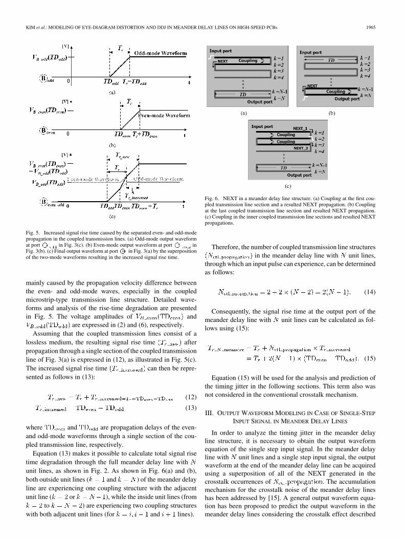
Fig. 5. Increased signal rise time caused by the separated even- and odd-modepropagation in the coupled transmission lines. (a) Odd-mode output waveformat port � in Fig. 3(c). (b) Even-mode output waveform at port � inFig. 3(b). (c) Final output waveform at port � in Fig. 3(a) by the superpositionof the two-mode waveforms resulting in the increased signal rise time.
mainly caused by the propagation velocity difference betweenthe even- and odd-mode waves, especially in the coupledmicrostrip-type transmission line structure. Detailed wave-forms and analysis of the rise-time degradation are presentedin Fig. 5. The voltage amplitudes of and
are expressed in (2) and (6), respectively.Assuming that the coupled transmission lines consist of a
lossless medium, the resulting signal rise time afterpropagation through a single section of the coupled transmissionline of Fig. 3(a) is expressed in (12), as illustrated in Fig. 5(c).The increased signal rise time can then be repre-sented as follows in (13):
(12)
(13)
where and are propagation delays of the even-and odd-mode waveforms through a single section of the cou-pled transmission line, respectively.
Equation (13) makes it possible to calculate total signal risetime degradation through the full meander delay line withunit lines, as shown in Fig. 2. As shown in Fig. 6(a) and (b),both outside unit lines ( and ) of the meander delayline are experiencing one coupling structure with the adjacentunit line ( or ), while the inside unit lines (from
to ) are experiencing two coupling structureswith both adjacent unit lines (for and lines).
Fig. 6. NEXT in a meander delay line structure. (a) Coupling at the first cou-pled transmission line section and a resulted NEXT propagation. (b) Couplingat the last coupled transmission line section and resulted NEXT propagation.(c) Coupling in the inner coupled transmission line sections and resulted NEXTpropagations.
Therefore, the number of coupled transmission line structuresin the meander delay line with unit lines,
through which an input pulse can experience, can be determinedas follows:
(14)
Consequently, the signal rise time at the output port of themeander delay line with unit lines can be calculated as fol-lows using (15):
(15)
Equation (15) will be used for the analysis and prediction ofthe timing jitter in the following sections. This term also wasnot considered in the conventional crosstalk mechanism.
III. OUTPUT WAVEFORM MODELING IN CASE OF SINGLE-STEP
INPUT SIGNAL IN MEANDER DELAY LINES
In order to analyze the timing jitter in the meander delayline structure, it is necessary to obtain the output waveformequation of the single step input signal. In the meander delayline with unit lines and a single step input signal, the outputwaveform at the end of the meander delay line can be acquiredusing a superposition of all of the NEXT generated in thecrosstalk occurrences of . The accumulationmechanism for the crosstalk noise of the meander delay lineshas been addressed by [15]. A general output waveform equa-tion has been proposed to predict the output waveform in themeander delay lines considering the crosstalk effect described

1966 IEEE TRANSACTIONS ON MICROWAVE THEORY AND TECHNIQUES, VOL. 56, NO. 8, AUGUST 2008
Fig. 7. Output waveform analysis of a meander line with � unit lines in caseof single step input signal, where TD means the propagation delay time of oneunit line. The source step pulse with a voltage amplitude of � and a rise timeof � is injected at the input port through a 50-� source impedance at � � �.
in (16), shown at the bottom of this page, where is the unitstep function.
To clarify the general output waveform equation in the me-ander delay line with unit lines, as expressed in (16), theoutput waveform is plotted in Fig. 7. Nevertheless, the losslessassumption can cause small TD between each NEXT. It can in-duce a decrease of the piled NEXT voltage level after the orig-inal source input signal. This effect will be discussed later inthis paper.
IV. EYE DIAGRAM AND TIMING-JITTER ESTIMATION
IN MEANDER DELAY LINES
This section will analyze the eye diagram and jitter generationmechanism in the meander delay line based on the NEXT anal-ysis introduced in the previous sections, and will propose jitter-estimation equations using a relationship between the propaga-tion TD of one unit line and the unit interval (UI) of the pseudo-random bit sequence (PRBS). In Section IV-A, the predicted eyediagram and proposed jitter-estimation equations will be veri-fied by comparisons with eye diagram and jitter measurementsof the test vehicles.
Total jitter (TJ) is composed of random jitter (RJ) and deter-ministic jitter (DJ), and DDJ is one part of DJ [4], [5]. In themeander delay line case, DDJ is from inter-symbol interference(ISI) caused by the following two factors:
• ISI caused by the NEXT;• ISI caused by channel loss,Here, the DDJ due to the NEXT will also be analyzed as-
suming a lossless meander delay line because DDJ due to lossis very small and negligible. (Both simulation results of losslessand lossy medium show same DDJ.)
Fig. 8(a) shows a meander delay line of a PCB with unitlines with a PRBS input data. At first, the short unit line delaycase is when the unit line delay (TD) is much shorter than UI, asdescribed in (17). In order to simplify the analysis, a data patternof “ ” is fed into the input port of the meander delay line
(short unit line delay case) (17)
(long unit line delay case) (18)
Fig. 8. (a) Meander delay line with � unit lines with the PRBS input data.(b) Induced NEXT caused by the rising/falling edges of the input step pulse.The PRBS data with voltage amplitude of � and a rise time of � is injectedat the input port through a 50-� source impedance.
where is the propagation TD of one unit line,is the velocity of the waveform for a microstrip line,
and is the length of one unit line.Fig. 8(b) presents the NEXT waveforms by rising and falling
edges, as previously explained in Fig. 7. A rising edge of theinput step pulse generates the NEXT with a positive voltage inthe output waveform. Similarly, a falling edge also induces theNEXT with a negative voltage.
A. Case of the Long Unit Line Delay
When is equal to or greater than UI, the output wave-form is affected by the NEXT at the rising and falling edgesover the entire UI, as shown in Fig. 9. The NEXT occurs be-fore and after the transitions when , as shown inFig. 7. Therefore, the expected output waveform and the eyediagram can be described as shown in Fig. 9(a) and (b), respec-tively. It should be noted that the eye diagram has three discretehigh levels around , and three discrete low levelsaround , regardless of the number of unit lines . Thethree high-voltage levels consist of the positive NEXT by therising edge, the original high input voltage level, and the neg-ative NEXT by the falling edge. In a similar manner, the threelow-voltage levels are the positive NEXT by the rising edge, theoriginal low input voltage level, and the negative NEXT by thefalling edge.
An expanded eye diagram is shown in Fig. 10 for the case ofthe long unit line delay. Since there are three high-voltage levelsand three low-voltage levels, respectively, there are also threecrossing points at rising and falling edges of the eye diagram. Inthis way, it is found that DDJ is produced in the case of the long
Output waveform (16)

KIM et al.: MODELING OF EYE-DIAGRAM DISTORTION AND DDJ IN MEANDER DELAY LINES ON HIGH-SPEED PCBs 1967
Fig. 9. Case of a long unit line delay in the meander delay line with � unitlines. The PRBS data with voltage amplitude of � and a rise time of � is in-jected at the input port through a 50-� source impedance. (a) Output waveform.(b) Expected eye diagram.
Fig. 10. Expanded eye diagram for the case of the long unit line delay in themeander delay line with � unit lines.
unit line delay, whereas DDJ is not generated in the case of theshort unit line delay, which will be shown in Section V. Sincethe DDJ can be characterized by the width across these crossingpoints, the jitter equation can be extracted in order to estimateDDJ amount [4].
To extract a jitter-estimation equation for the case of the longunit delay line, the eye diagram at the rising edge is depictedin Fig. 11(a). If the meander delay line has unit lines, theaccumulated NEXT, which decides the three levels in the ex-panded eye diagram, is , while thisvalue is shown in (16) and Fig. 7. The jitter-estimation equationcan then be extracted using a triangle principle, as demonstrated
Fig. 11. Extraction of the timing jitter �� � for the case of the long unitdelay line in the meander delay line with � unit lines. (a) At the rising edge.(b) Triangle principle to calculate the timing jitter �� �.
in Fig. 11(b). From Fig. 11(b), the following relations can beinduced:
(19)
Therefore, the proposed jitter-estimation equation for the caseof the long unit line delay in the meander line with unit linescan be represented as
if (long unit line delay case) (20)
The timing jitter is seen to be heavily dependent onthe number of unit lines , the main NEXT coef-ficient , and the increased signal rise time
. The increased signal rise timeat the output port will also increase proportion-
ally to the number of unit lines . As a result,increases proportionately to the square of the number of unitlines . This means that the NEXT at the meanderdelay line can cause a significant amount of timing jitter,especially when there are many unit lines. Using this proposedjitter-estimation equation (20), the timing jitter can be estimatedfor the case of the long line delay in meander delay lines with
unit lines.
B. Case of the Short Unit Line Delay
As shown in Fig. 12, since is much smaller than UI, theinduced NEXT by the rising and falling edges occupies only asmall portion of the duration of the UI. As a consequence, theeye diagram can be depicted as shown in Fig. 12(b).
An expanded eye diagram of Fig. 12(b) is redrawn in Fig. 13.It illustrates the crossing points of the output waveform at therising and the falling edges with respect to the ideal crossingpoints. It is found that real crossing points are shifted by theamount of at both edges in the eye diagram due tothe NEXT. However, the time interval between the two crossingpoints stays the same as the UI. Therefore, DDJ is not generatedin the case of the short unit line delay due to the NEXT. How-ever, the total propagation TD along the meander delay line
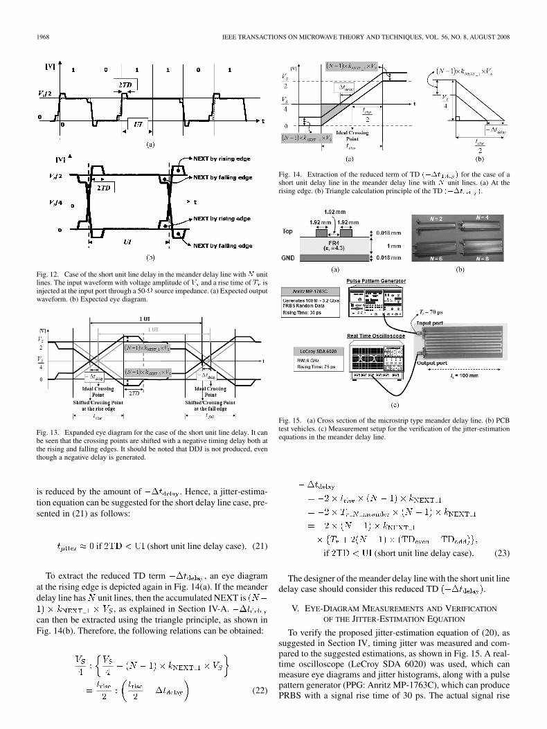
1968 IEEE TRANSACTIONS ON MICROWAVE THEORY AND TECHNIQUES, VOL. 56, NO. 8, AUGUST 2008
Fig. 12. Case of the short unit line delay in the meander delay line with � unitlines. The input waveform with voltage amplitude of � and a rise time of � isinjected at the input port through a 50-� source impedance. (a) Expected outputwaveform. (b) Expected eye diagram.
Fig. 13. Expanded eye diagram for the case of the short unit line delay. It canbe seen that the crossing points are shifted with a negative timing delay both atthe rising and falling edges. It should be noted that DDJ is not produced, eventhough a negative delay is generated.
is reduced by the amount of . Hence, a jitter-estima-tion equation can be suggested for the short delay line case, pre-sented in (21) as follows:
if (short unit line delay case) (21)
To extract the reduced TD term , an eye diagramat the rising edge is depicted again in Fig. 14(a). If the meanderdelay line has unit lines, then the accumulated NEXT is
, as explained in Section IV-A.can then be extracted using the triangle principle, as shown inFig. 14(b). Therefore, the following relations can be obtained:
(22)
Fig. 14. Extraction of the reduced term of TD ���� � for the case of ashort unit delay line in the meander delay line with � unit lines. (a) At therising edge. (b) Triangle calculation principle of the TD ���� �.
Fig. 15. (a) Cross section of the microstrip type meander delay line. (b) PCBtest vehicles. (c) Measurement setup for the verification of the jitter-estimationequations in the meander delay line.
if (short unit line delay case) (23)
The designer of the meander delay line with the short unit linedelay case should consider this reduced TD .
V. EYE-DIAGRAM MEASUREMENTS AND VERIFICATION
OF THE JITTER-ESTIMATION EQUATION
To verify the proposed jitter-estimation equation of (20), assuggested in Section IV, timing jitter was measured and com-pared to the suggested estimations, as shown in Fig. 15. A real-time oscilloscope (LeCroy SDA 6020) was used, which canmeasure eye diagrams and jitter histograms, along with a pulsepattern generator (PPG: Anritz MP-1763C), which can producePRBS with a signal rise time of 30 ps. The actual signal rise

KIM et al.: MODELING OF EYE-DIAGRAM DISTORTION AND DDJ IN MEANDER DELAY LINES ON HIGH-SPEED PCBs 1969
Fig. 16. Eye diagram and jitter measurements for the case of the long unit linedelay in the meander delay line with eight unit lines �� � ��, where the lengthof one unit line �� � is 100 mm. The data rate of the input data is 1 Gb/s. TDis 0.62 ns and UI is 1 ns. Therefore, this is a long unit line delay case ���� ���, as shown in (18). (a) Measured eye diagram. (b) Measured jitter histogram.(c) Measured DDJ value.
time fed into the input port of the meander delay line is 70 psbecause of the cable loss. The real-time oscilloscope can extractRJ, DJ, and TJ from the timing-jitter measurements. It also canseparate DDJ and PJ from the extracted DJ [5].
In order to verify the proposed jitter-estimation equations, aseries of microstrip type test vehicles with the meander delayline were fabricated and tested. In the test vehicles, is fixedto 100 mm. In addition, is varied from two to eight, as shownin Fig. 15(b), to investigate the suggested jitter-estimation equa-tions that are dependent on . The eye diagram and the timingjitter for the two cases of the long unit line delay and the shortunit line delay were obtained. Since the length of one unit linewas fixed , two UIs of the PRBS input data were selected forseparation between the long and short unit delay line cases.
A. Eye Diagram and Jitter Measurements for the Caseof the Long Unit Line Delay
The timing jitter was first analyzed for the case of a long unitline with eight unit lines . When is eight and is100 mm, the increased rise time due to the even/odd-mode prop-agation mismatch can be calculated using (15). Furthermore, theNEXT coefficient is evaluated by (10)
ps ps ps
The amount of the timing jitter by the NEXT can then be es-timated using the proposed jitter-estimation equation (20). Thisestimated timing jitter is the DDJ caused by the NEXT in themeander delay line
ps ps (24)
Fig. 16 shows the measured eye diagram and the jitterhistogram of the meander delay line with and
mm. As shown in Fig. 16(a), the measuredeye-diagram distinctively exhibits three crossing points ( ,and ). The measured timing jitter is then 253.8 ps, as shownin Fig. 16(b) and (c). It can be noted that the measured timing
Fig. 17. Blurred eye diagram and the blurred jitter histogram for the case of thelong unit line delay to interpret the sub-peaks in the measured jitter histogramcaused by the channel loss in Fig. 16.
Fig. 18. Comparisons between estimated by the proposed equation simulatedby EM/circuit simulator and measured DDJ for the case of the long unit linedelay, where � � �� mm. The data rate of the input PRBS is 1 Gb/s. TD is0.62 ns and UI is 1 ns. Therefore, this is a long unit line delay case ���� � ��,as shown in (18).
jitter of 253.8 ps is fairly close to the estimated timing jitterin (24) confirming the validity of the proposed analysis andequations. This unique eye diagram with each three high andlow levels agrees very well with the analysis of the timing-jittermechanism by the NEXT through the lossless assumption.
However, as shown in Fig. 16(b), the jitter histogram has sub-peaks inside the main three peaks. These sub-peaks can be pro-duced by blurred NEXT levels and blurred rising edge causedby the channel loss, as described in Fig. 17. Since each NEXTlevel will blur the same amount, the shape of the sub-peaks willthen be like Fig. 17. As discussed in Fig. 10, the jitter histogramis supposed to have three discrete peaks originating from thethree crossing points in the eye diagram.
Fig. 18 shows the tendency of the timing jitter highly de-pending on . It shows the measured, simulated, and the es-timated DDJ for the cases of a long unit line delay with
mm and varied . It should be stated that the NEXT pro-duces a significant amount of the DDJ, as can be seen fromthe measurements, simulations, and estimations. For the timing-jitter simulation, -parameters of each pattern were extractedby Ansoft’s Design System EM solver, and then they were im-ported in Agilent’s Advanced Design System (ADS). For accu-rate simulation results, the simulated frequency was from dc to20 GHz and the accumulated time was 1 s (1-ps step). In the
1970 IEEE TRANSACTIONS ON MICROWAVE THEORY AND TECHNIQUES, VOL. 56, NO. 8, AUGUST 2008
Fig. 19. Predicted and measured output waveform in the meander delay linewith � � � and � � ��� mm.
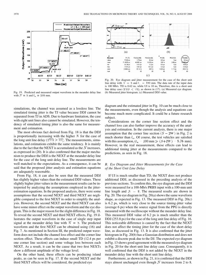
simulations, the channel was assumed as a lossless line. Thesimulated timing jitter is the TJ value because DDJ cannot beseparated from TJ in ADS. Due to hardware limitation, the casewith eight unit lines also cannot be simulated. However, the ten-dency of simulated timing jitter is also the same for measure-ment and estimation.
The most obvious fact derived from Fig. 18 is that the DDJis proportionally increasing with the higher for the case ofthe long unit line delay . The measurements, simu-lations, and estimations exhibit the same tendency. It is mainlydue to the fact that the NEXT is accumulated as the increases,as expressed in (20). It is also confirmed that the major mecha-nism to produce the DDJ is the NEXT at the meander delay linefor the case of the long unit delay line. The measurements arewell matched to the expectations. As a consequence, it can besaid that the proposed jitter analysis and estimation equationsare adequately reasonable.
From Fig. 18, it can also be seen that the measured DDJhas slightly higher values than the estimated DDJ values. Theseslightly higher jitter values in the measurement results can be in-terpreted by analyzing the assumptions employed in the jitter-estimation equations. In the proposed analysis, there were someassumptions that the second NEXT and third NEXT are negli-gible compared to the first NEXT in order to simplify the anal-ysis. However, the second NEXT and the third NEXT can alsohave some minor effect on the output waveform and the eye dia-gram. This is the major reason for the slight difference in Fig. 18.To reveal the second NEXT and third NEXT effects, Fig. 19 il-lustrates the output waveform in the case of single step inputsignal at the meander delay line with . The predictedwaveform and the first NEXT can be obtained using (16) andFig. 7. As mentioned in Section III, the predicted output wave-form does not include the channel loss effect and the corner linesection effect. These effects can induce small TD (12.4 ps perone corner line section) and some voltage loss between eachNEXT. As a result, it can be the cause that two first NEXTsshow a different amplitude of the voltage level.
On the other hand, these effects can be producing islandpeaks, as can be seen in Fig. 17. If the second NEXT and thethird NEXT effects will be considered, the predicted eye
Fig. 20. Eye diagram and jitter measurement for the case of the short unitline delay with � � � and � � ��� mm. The data rate of the input datais 100 Mb/s. TD is 0.62 ns, while UI is 10 ns, Therefore, this is a short unitline delay case ���� � �, as shown in (17). (a) Measured eye diagram.(b) Measured jitter histogram. (c) Measured DDJ value.
diagram and the estimated jitter in Fig. 10 can be much close tothe measurements, even though the analysis and equations canbecome much more complicated. It could be a future researchsubject.
Considerations on the corner line section effect and thechannel loss can also further improve the accuracy of the anal-ysis and estimation. In the current analysis, there is one majorassumption that the corner line section in Fig. 2 ismuch shorter than . Of course, the test vehicles are satisfiedwith this assumption, ( mm mm).However, in the real measurement, these effects can lead toadditional timing jitter at the measurements compared to thepredictions, as seen in Fig. 18.
B. Eye Diagram and Jitter Measurements for the Caseof the Short Unit Line Delay
If UI is much smaller than TD, the NEXT does not produceadditional DDJ, as discussed in the preceding analysis of theprevious sections. To confirm this, the eye diagram and the DDJwere measured for a 100-Mb/s PRBS input with a 100-mm unitline length and . The measured results are shown inFig. 20. The eye diagram in Fig. 20(a) shows the same waveformshape, as expected in Fig. 13. The measured DDJ in Fig. 20(c)is 6.2 ps, which is very close to the source timing-jitter value(average 6 ps) when the source signal from the PPG is directlymeasured with the oscilloscope without the meander delay line.This measured DDJ value of 6.2 ps is much smaller than theDDJ (253.8 ps) for the case of the long unit line delay of Fig. 16.This noticeable difference is caused by the fact that the NEXTdoes not affect the timing jitter for the case of the short delayline, as discussed in Fig. 13. It is also confirmed that the jitterhistogram in Fig. 20(b) has a Gaussian distribution and does notexhibit a discrete peak due to the DJ. The expected eye diagramin Fig. 13 shows good agreement with the measured eye diagramin Fig. 20 for the short unit line delay case. Consequently, it iswell confirmed that the DDJ is not added by the NEXT in themeander delay line with the short unit line delay.
Furthermore, as shown in Fig. 21, it is confirmed that the DDJstays almost unchanged even though increases from 2 to 8.

KIM et al.: MODELING OF EYE-DIAGRAM DISTORTION AND DDJ IN MEANDER DELAY LINES ON HIGH-SPEED PCBs 1971
Fig. 21. Comparisons between estimated by the proposed equation, simulatedby EM/circuit co-simulation, and measured DDJ for the short unit line delaycase with respect to � (from � � � to � � �) and � � ��� mm. The datarate of the input data is 100 Mb/s.
Fig. 22. Two designs of a meander delay line with a fixed total line length anda fixed data rate. (a) Short unit line delay case with small timing jitter. (b) Longunit line delay case with small NEXT.
On the other hand, the DDJ increases with for the case of thelong unit line delay.
If the data rate of the input PRBS is 1 Gb/s and the unit linelength of the meander delay line is reduced to 10 mm (mm), then TD is 62 ps and ns. Therefore, this is anothercondition to meet the short unit line delay case ,and the same result of small jitter will be presented as shown inFig. 21.
Consequently, it can be said that when designing a meanderdelay line on a PCB, the meander delay line, which meets thecondition of the short unit line delay case, as described in (17),is the better choice with respect to minimizing the timing jitter.The rule of thumb in designing a meander delay line with theminimal timing jitter caused by the NEXT is that should bekept as small as possible. On the other hand, increasing cancause excessive overshoot in the eye diagram of Fig. 13, whichis . Additionally, the meander delayline with the short unit line delay condition will produce thereduced TD term , as discussed in Fig. 14. It shouldbe considered when starting the design process by adding anextra delay line.
There is a tradeoff between the timing-jitter generation by theNEXT and the piled NEXT voltage in the eye diagram, whena meander delay line is designed with a fixed total line-length
. The short unit line delay case of Fig. 22(a)produces less timing jitter, but it has a large NEXT voltage level.If the number of unit lines is very large and the unit line lengthis not much larger than the corner line section, the assumption,which is the corner line section is much shorter than the lengthof the unit line, is not satisfied and the timing jitter is not exactly
estimated. This means that when it comes to the timing-jitterissue, the meander delay line should be designed as the shortunit line delay case. However, if the voltage margin is the mainconcern, the long unit line delay case of Fig. 22(b) is a betterdesign approach.
VI. CONCLUSION
This paper proposed an eye-diagram analysis method andjitter-estimation equations in the densely spaced meander delayline structure used in PCB designs based on the time-domaineven- and odd-mode analysis of a coupled transmission line.Eye-diagram distortion and an increased DDJ are caused byEM crosstalk noise between the closely spaced adjacent lines inthe meander delay line. In order to verify the proposed eye-di-agram analysis and the jitter-estimation equations, a series ofmicrostrip-type test vehicles were fabricated and tested. To fur-ther improve the analysis and estimation accuracy further, ad-ditional timing-jitter sources at the meander delay line causedby high-frequency dielectric and conductor loss should be ac-counted. The proposed method can be also applied to analyzeeye-diagram distortion and jitter generation in a stripline-typemeander delay line structure. The proposed analysis will be usedto investigate the eye-diagram distortion and the jitter generationin the case of a 3-D meander delay line structure in a multilayerPCB with vertical vias in order to save the surface area of themeander delay line further. The proposed analysis provides ananalytic interpretation approach, which is more efficient thanEM/circuit co-simulation.
REFERENCES
[1] H. Bakoglu, Circuits, Interconnections, and Packaging forVLSI. New York: Addison-Wesley, 1990, ch. 8.
[2] B. J. Rubin, “Study of meander line delay in circuit boards,” IEEETrans. Microw. Theory Tech., vol. 48, no. 9, pp. 1452–2000, Sep. 2000.
[3] O. M. Ramahi, “Analysis of conventional and novel delay lines: A nu-merical study,” J. Appl. Comput. Electromagn. Soc., vol. 18, no. 3, pp.181–190, Nov. 2003.
[4] Jitter Fundamentals Wavecrest Corporation, Eden Prairie, MN,2006. [Online]. Available: http://www.wavecrest.com/technical/pdf/Jitter_Fundamentals.pdf
[5] “Serial Data Analyzers Manual” LeCory Corporation, ChestnutRidge, NY, 2006. [Online]. Available: http://www.lecroy.com/tm/products/Analyzers/SDA/SDA_Brochure.pdf
[6] R. Wu and F. Chao, “Laddering wave in serpentine delay line,” IEEETrans. Compon., Packag., Manuf. Technol., vol. 18, no. 4, pp. 644–650,Nov. 1995.
[7] H. Lee et al., “Unit cell approach to full-wave analysis of meanderdelay line using FDTD periodic structure modeling method,” IEEETrans. Adv. Packag., vol. 25, no. 2, pp. 215–222, May 2002.
[8] R. Wu and F. Chao, “Flat spiral delay line design with minimumcrosstalk penalty,” IEEE Trans. Compon., Packag., Manuf. Technol.,vol. 19, no. 2, pp. 397–402, May 1996.
[9] W. Guo et al., “Comparisons between serpentine and flat spiraldelay lines on transient reflection/transmission waveforms and eyediagrams,” IEEE Trans. Microw. Theory Tech., vol. 54, no. 4, pt. 1, pp.1379–1387, Apr. 2006.
[10] S. H. Hall et al., High-Speed Digital System Design, A Handbook ofInterconnect Theory and Design Practices.. New York: Wiley, 2000,pp. 42–73.
[11] M. Sung et al., “An efficient crosstalk parameter extraction method forhigh-speed interconnection lines,” IEEE Trans. Adv. Packag., vol. 23,pp. 148–155, May 2000.
[12] K. C. Gupta et al., Microstrip Lines and Slotlines, 2nd ed. Boston,MA: Artech House, 2000, ch. 3.
[13] W. J. Dally and J. W. Poulton, Digital Systems Engineering. NewYork: Cambridge Univ. Press, 1998, ch. 6.
[14] R. Garg and I. J. Bahl, “Characteristics of coupled microstriplines,”IEEE Trans. Microw. Theory Tech., vol. MTT-27, no. 7, pp. 700–705,Jul. 1979.

1972 IEEE TRANSACTIONS ON MICROWAVE THEORY AND TECHNIQUES, VOL. 56, NO. 8, AUGUST 2008
[15] G. Kim et al., “TDR/TDT analysis by crosstalk in single and differen-tial meander delay lines for high speed PCB applications,” in IEEE Int.Electromagn. Compat. Symp., Aug. 2006, vol. 3, pp. 657–662.
[16] E. Song et al., “Estimation of data-dependent jitter using single pulseanalysis method in high-speed differential signaling,” in IEEE Int.Electromagn. Compat. Symp., Sep. 2006, vol. 2, pp. 741–746.
Gawon Kim (S’06) received the B.S. degree inelectrical engineering from Kyungpook NationalUniversity, Daegu, Korea, in 2003, the M.S. degreein electrical engineering from the Korea AdvancedInstitute of Science and Technology (KAIST), Dae-jeon, Korea, in 2006, respectively, and is currentlyworking toward the Ph.D. degree at KAIST.
Her current research interests include signalintegrity issue in meander delay lines and 3-D delayline structure for system-in-package design.
Dong Gun Kam (M’06) received the B.S. degree inphysics and M.S. and Ph.D. degrees in electrical engi-neering from he Korea Advanced Institute of Scienceand Technology (KAIST), Daejeon, Korea, in 2002,2002 and 2006, respectively.
He is currently with the IBM T. J. Watson Re-search Center, Yorktown Heights, NY. His researchinterests include design and characterization ofhigh-speed input/output (I/O) subsystems.
Seung Jae Lee (M’99) received the B.S. degree inelectrical engineering from Yeungnam University,Gyeongsan, Korea, in 2001, and the M.S. degreein electronic engineering from the Information andCommunication University (ICU), Daejeon, Korea,in 2003, respectively.
He is currently with the Corporate Research andDevelopment Center, Amkor Technology Korea Inc.,Seoul, Korea. His research interests include signalintegrity, power integrity, and RF issues in packagedesign.
Jaemin Kim (S’06) received the B.S. degree inelectrical and electronic engineering from YonseiUniversity, Seoul, Korea, in 2003, the M.S. degreein electrical engineering from the Korea AdvancedInstitute of Science and Technology (KAIST), Dae-jeon, Korea, in 2006, respectively, and is currentlyworking toward the Ph.D. degree at KAIST.
His current research interests include RFmixed-mode system-in-package design andchip-package-PCB power distribution networkco-design and co-simulation methodology.
Myunghyun Ha (S’06) received the B.S. and M.S.degrees in electrical engineering from the KoreaAdvanced Institute of Science and Technology(KAIST), Korea, in 2004 and 2007, respectively,and is currently working toward the Ph.D. degree inelectrical and computer engineering at the GeorgiaInstitute of Technology, Atlanta.
His research interests are time- and frequency-do-main EM field simulation method using orthogonalfunctions that enables chip-package co-simulation.
Kyoungchoul Koo (S’06) received the B.S. degree inelectrical engineering from the Korea Advanced In-stitute of Science and Technology (KAIST), Daejeon,Korea, in 2005.
He is currently with the Department of ElectricalEngineering, KAIST. His research interest includesRF circuits and RF identification (RFID) reader unit.
Jun So Pak (M’02) received the B.S. degree inelectrical communication engineering from HanyangUniversity, Seoul, Korea, in 1998, and the M.S.and Ph.D. degrees in electrical engineering fromthe Korea Advanced Institute of Science and Tech-nology (KAIST), Daejeon, Korea, in 2000 and2005, respectively. His doctoral thesis concernedthe spice circuit type modeling technique (balancedtransmission-line matrix (TLM) and via couplingmodel) for the analysis of power/ground plane noiseand edge radiation in high-performance multilayer
PCBs and packages.In 2005, he was a Japan Society for the Promotion of Science (JSPS) Re-
search Fellow with the High Density Interconnection Group, National Insti-tute of Advanced Industrial Science and Technology (AIST), Tsukuba, Japan,where he was involved in the development of interconnection techniques for3-D multichip packaging. Since 2007, he has been a Research Professor withthe Department of Electrical Engineering, KAIST. His research interests are thedevelopment of 3-D stacked chip package using a through silicon vias (TSVs).
Joungho Kim (M’04) received the B.S. and M.S. de-grees in electrical engineering from Seoul NationalUniversity, Seoul, Korea, in 1984 and 1986, respec-tively, and the Ph.D. degree in electrical engineeringfrom The University of Michigan at Ann Arbor, in1993.
During his graduate study, he was involved withfemtosecond time-domain optical measurementtechniques for high-speed device and circuit testing.In 1993, he joined Picometric Inc., Ann Arbor, MI,where he was a Research Engineer responsible for
development of picosecond sampling systems and 70–GHz photoreceivers. In1994, he joined the Memory Division, Samsung Electronics, Kiheung, Korea,where he was involved with gigabit-scale dynamic RAM (DRAM) design.In 1996, he joined the Korea Advanced Institute of Science and Technology(KAIST), Taejon, Korea, where he is currently a Professor with the ElectricalEngineering and Computer Science Department. Since joining KAIST, hisresearch has focused on modeling, design, and measurement of high-speedinterconnections, packages, and PCBs. His research especially concernschip-package co-design and simulation for signal integrity, power integrity,ground integrity, timing integrity, and radiated emission in 3-D packages,system-in-package (SiP), system-on-package (SoP), and multilayer PCBs. Hehas successfully designed over ten SiPs for wireless communication applica-tions such as ZigBee, terrestrial digital multimedia broadcasting (T-DMB),near-field communication (NFC), and ultra-wideband (UWB). From 2001to 2002, he was on sabbatical leave during the academic year with SiliconImage Inc., Sunnyvale CA, as a Staff Engineer, where he was responsible forlow-noise package design of SATA, FC, and Panel Link SerDes devices. He iscurrently a Technical Consultant for automobile electromagnetic interference(EMI)/electromagnetic compatibility (EMC) design with Hyundai Motors Inc.He has authored or coauthored over 210 publications in refereed journals andconferences.
Dr. Kim has been the chair or co-chair of the EDAPS Workshop since2002. He is currently an associate editor for the IEEE TRANSACTIONS OF
ELECTROMAGNETIC COMPATIBILITY.