
iCE40 UltraLite™ Family Data Sheet - Home - Lattice ... Architecture iCE40 UltraLite Family Data...
37
iCE40 UltraLite™ Family Data Sheet DS1050 Version 1.4, November 2016
Transcript of iCE40 UltraLite™ Family Data Sheet - Home - Lattice ... Architecture iCE40 UltraLite Family Data...

iCE40 UltraLite™ Family Data SheetDS1050 Version 1.4, November 2016

www.latticesemi.com 1-1 DS1050 Introduction_01.2
July 2016 Data Sheet DS1050
© 2016 Lattice Semiconductor Corp. All Lattice trademarks, registered trademarks, patents, and disclaimers are as listed at www.latticesemi.com/legal. All other brand or product names are trademarks or registered trademarks of their respective holders. The specifications and information herein are subject to change without notice.
General DescriptioniCE40 UltraLite family is an optimum logic, smallest footprint, low I/O count ultra-low power FPGA and sensor man-ager with instant on capability. It is designed for ultra-low power mobile applications, such as smartphones, tablets and hand-held devices. The iCE40 UltraLite family includes integrated blocks to interface with virtually all mobile sensors and application processors. The iCE40 UltraLite family also features two on-chip oscillators, 10 kHz and 48 MHz. The LFOSC (10 kHz) is ideal for low power function in always-on applications, while HFOSC (48 MHz) can be used for awaken activities.
The hardened RGB PWM IP, with the three 24 mA constant current RGB LED outputs on the iCE40 UltraLite pro-vides all the necessary logic to directly drive the service LED, without the need of external MOSFET or buffer.
The 400 mA constant current IR driver output provides a direct interface to external LED for application such as IrDA functions. Users simply implement the hardened TX/RX pulse logic that meets their needs, and connect the IR driver directly to the LED, without the need of external MOSFET or buffer. The 100 mA Barcode Emulation driver output provides a direct interface for applications such as barcode scanning. The 100 mA and 400 mA drivers can also be combined to be used as a 500 mA IR driver if higher than 400 mA current drive is required.
The iCE40 UltraLite family of devices are targeting for mobile applications to perform functions such as IrDA, Ser-vice LED, Barcode Emulation, GPIO Expander, SDIO Level Shift, and other custom functions.
The iCE40 UltraLite family features two device densities of 640 or 1K Look Up Tables (LUTs) of logic with program-mable I/Os that can be used as an interface port or general purpose I/O. It also has up to 56 kbits of Block RAMs to work with user logic.
iCE40 UltraLite Family Data SheetIntroduction
Features Flexible Logic Architecture
• Two devices with 640 or 1K LUTs• Offered in 16-ball WLCSP package• Offered in 36-ball ucBGA package
Ultra-low Power Devices• Advanced 40 nm ultra-low power process• Typical 35 µA standby current which equals
42 uW standby power consumption
Embedded and Distributed Memory• Up to 56 kbits sysMEM™ Embedded Block RAM
Two Hardened Interfaces• Two optional FIFO mode I2C interface up to
1 MHz• Either master or slave
Two On-Chip Oscillators• Low Frequency Oscillator - 10 kHz• High Frequency Oscillator - 48 MHz
Hardened PWM circuit for RGB
Hardened TX/RX Pulse Logic circuit for IR LED
24 mA Current Drive RGB LED Outputs• Three drive outputs in each device• User selectable sink current up to 24 mA
400 or 500 mA Current Drive IR LED Output• One IR drive output in each device• User selectable sink current up to 400 mA• Can be combined with 100 mA Barcode driver to
form 500 mA IR driver
100 mA Current Drive Barcode Emulator• One barcode driver output in each device• User selectable sink current up to 100 mA• Can be combined with 400 mA IR driver to use
as 500 mA IR driver
Flexible On-Chip Clocking• Eight low skew global signal resource, six can
be directly driven from external pins• One PLL with dynamic interface per device

1-2
IntroductioniCE40 UltraLite Family Data Sheet
Flexible Device Configuration• SRAM is configured through:
— Standard SPI Interface— Internal Nonvolatile Configuration Memory
(NVCM)
Ultra-Small Form Factor• As small as 1.409 mm x 1.409 mm
Applications• Smartphones• Tablets and Consumer Handheld Devices• Handheld Industrial Devices• Multi Sensor Management Applications• IR remote, Barcode emulator• RGB light control
Table 1-1. iCE40 UltraLite Family Selection Guide
IntroductionThe iCE40 UltraLite devices are fabricated on a 40 nm CMOS low power process. The device architecture has sev-eral features such as user configurable RGB LED and IR LED Controllers, and two Oscillators.
The iCE40 UltraLite FPGAs are available in very small form factor packages, as small as 1.409 mm x 1.409 mm. The small form factor allows the device to easily fit into a lot of mobile applications. Table 1-1 shows the LUT densi-ties, package and I/O pin count.
The iCE40 UltraLite devices offer I/O features such as programmable multiple value pull-up resistors. Pull-up fea-tures are controllable on a “per-pin” basis.
The iCE40 UltraLite devices also provide flexible, reliable and secure configuration from on-chip NVCM. These devices can also configure themselves from external SPI Flash, or be configured by an external master such as a CPU.
Lattice provides a variety of design tools that allow complex designs to be efficiently implemented using the iCE40 UltraLite family of devices. Popular logic synthesis tools provide synthesis library support for iCE40 UltraLite. Lat-tice design tools use the synthesis tool output along with the user-specified preferences and constraints to place and route the design in the iCE40 UltraLite device. These tools extract the timing from the routing and back-anno-tate it into the design for timing verification.
Part Number iCE40UL-640 iCE40UL-1K
Logic Cells (LUT + Flip-Flop) 640 1248
EBR Memory Blocks 14 14
EBR Memory Bits 56 k 56 k
PLL Block1 1 1
Hardened I2C 2 2
Hardened IR TX/RX 1 1
Hardened RGB PWM IP 1 1
HF Oscillator (48 MHz) 1 1
LF Oscillator (10 kHz) 1 1
24 mA LED Sink 3 3
100 mA LED Sink 1 1
400 mA LED Sink 1 1
Packages, ball pitch, dimension Programmable I/O Count
16-ball WLCSP, 0.35 mm, 1.409 mm x 1.409 mm 10 10
36-ball ucBGA, 0.40 mm, 2.5 mm x 2.5 mm 26 26
1. Only in 36-ball ucBGA package.

1-3
IntroductioniCE40 UltraLite Family Data Sheet
Lattice provides many pre-engineered IP (Intellectual Property) modules, including a number of reference designs, licensed free of charge, optimized for the iCE40 UltraLite FPGA family. Lattice also can provide fully verified bit-stream for some of the widely used target functions in mobile device applications, such as IR remote, barcode emu-lator, and RGB LED control functions. Users can use these functions as offered by Lattice, or they can use the design to create their own unique required functions. For more information regarding Lattice's reference designs or fully-verified bitstreams, please contact your local Lattice representative.

www.latticesemi.com 2-1 DS1050 Architecture_01.2
July 2016 Data Sheet DS1050
© 2016 Lattice Semiconductor Corp. All Lattice trademarks, registered trademarks, patents, and disclaimers are as listed at www.latticesemi.com/legal. All other brand or product names are trademarks or registered trademarks of their respective holders. The specifications and information herein are subject to change without notice.
Architecture OverviewThe iCE40 UltraLite family architecture contains an array of Programmable Logic Blocks (PLB), two Oscillator Gen-erators, two user configurable I2C controllers, and blocks of sysMEM™ Embedded Block RAM (EBR) surrounded by Programmable I/O (PIO). Figure 2-1shows the block diagram of the iCE40UL-1K device.
Figure 2-1. iCE40UL-1K Device, Top View
The logic blocks, Programmable Logic Blocks (PLB) and sysMEM EBR blocks, are arranged in a two-dimensional grid with rows and columns. Each column has either PLB or EBR blocks. The PIO cells are located at the top and bottom of the device, arranged in banks. The PLB contains the building blocks for logic, arithmetic, and register functions. The PIOs utilize a flexible I/O buffer referred to as a sysIO buffer that supports operation with a variety of interface standards. The blocks are connected with many vertical and horizontal routing channel resources. The place and route software tool automatically allocates these routing resources.
In the iCE40 UltraLite family, there are three sysIO banks, one on top and two at the bottom. User can connect all VCCIOs together, if all the I/Os are using the same voltage standard. Refer to the details in later sections of this doc-ument. The sysMEM EBRs are large 4 kbit, dedicated fast memory blocks. These blocks can be configured as RAM, ROM or FIFO with user logic using PLBs.
The iCE40 UltraLite also includes two user I2C ports, two Oscillators, and high current RGB and IR LED sinks, and a 100 mA Barcode emulation output.
4 4
kbi
t RAM
4 4
kbi
t RAM
3 4
kbi
t RAM
3 4
kbi
t RAM
PLB
I/O Bank 0
I/O Bank 2
HFOSC LFOSC
config
I/O Bank 1
NVCM
IR and Barcode Drv
RGB Drv
Flip-flop with Enableand Reset Controls
Carry Logic4-Input Look-up
Table (LUT)8
Logi
c C
ells
= P
rogr
amm
able
Log
ic B
lock
I2CI2C
iCE40 UltraLite Family Data SheetArchitecture

2-2
ArchitectureiCE40 UltraLite Family Data Sheet
PLB BlocksThe core of the iCE40 UltraLite device consists of Programmable Logic Blocks (PLB) which can be programmed to perform logic and arithmetic functions. Each PLB consists of eight interconnected Logic Cells (LC) as shown in Figure 2-2. Each LC contains one LUT and one register.
Figure 2-2. PLB Block Diagram
Logic CellsEach Logic Cell includes three primary logic elements shown in Figure 2-2.
• A four-input Look-Up Table (LUT) builds any combinational logic function, of any complexity, requiring up to four inputs. Similarly, the LUT element behaves as a 16x1 Read-Only Memory (ROM). Combine and cascade multiple LUTs to create wider logic functions.
• A ‘D’-style Flip-Flop (DFF), with an optional clock-enable and reset control input, builds sequential logic func-tions. Each DFF also connects to a global reset signal that is automatically asserted immediately following device configuration.
• Carry Logic boosts the logic efficiency and performance of arithmetic functions, including adders, subtracters, comparators, binary counters and some wide, cascaded logic functions.
Table 2-1. Logic Cell Signal Descriptions
Function Type Signal Names Description
Input Data signal I0, I1, I2, I3 Inputs to LUT
Input Control signal Enable Clock enable shared by all LCs in the PLB
Input Control signal Set/Reset1 Asynchronous or synchronous local set/reset shared by all LCs in the PLB.
Input Control signal Clock Clock one of the eight Global Buffers, or from the general-purpose interconnects fabric shared by all LCs in the PLB
Input Inter-PLB signal FCIN Fast carry in
Output Data signals O LUT or registered output
Output Inter-PFU signal FCOUT Fast carry out
1. If Set/Reset is not used, then the flip-flop is never set/reset, except when cleared immediately after configuration.
= Statically defined by configuration program
LUT
Carry Logic
Logic Cell
SR
EN
D Q
DFF
Flip-flop with optional enable and set or reset controls
Four-inputLook-Up Table(LUT)
Clock
EnableFCOUT
FCIN
Set/Reset
Shared Block-Level Controls
Programmable LogicBlock (PLB)
8 Lo
gic
Cel
ls (
LCs)
I0
I1
I2
I3
O
1
0

2-3
ArchitectureiCE40 UltraLite Family Data Sheet
RoutingThere are many resources provided in the iCE40 UltraLite devices to route signals individually with related control signals. The routing resources consist of switching circuitry, buffers and metal interconnect (routing) segments.
The inter-PLB connections are made with three different types of routing resources: Adjacent (spans two PLBs), x4 (spans five PLBs) and x12 (spans thirteen PLBs). The Adjacent, x4 and x12 connections provide fast and efficient connections in the diagonal, horizontal and vertical directions.
The design tool takes the output of the synthesis tool and places and routes the design.
Clock/Control Distribution NetworkEach iCE40 UltraLite device has six global inputs, two pins on the top bank and four pins on the bottom bank
These global inputs can be used as high fanout nets, clock, reset or enable signals. The dedicated global pins are identified as Gxx and each drives one of the eight global buffers. The global buffers are identified as GBUF[7:0]. These six inputs may be used as general purpose I/O if they are not used to drive the clock nets.
Table 2-2 lists the connections between a specific global buffer and the inputs on a PLB. All global buffers optionally connect to the PLB CLK input. Any four of the eight global buffers can drive logic inputs to a PLB. Even-numbered global buffers optionally drive the Set/Reset input to a PLB. Similarly, odd-numbered buffers optionally drive the PLB clock-enable input. GBUF[7:6, 3:0] can connect directly to G[7:6, 3:0] pins respectively. GBUF4 and GBUF5 can connect to the two on-chip Oscillator Generators (GBUF4 connects to LFOSC, GBUF5 connects to HFOSC).
Table 2-2. Global Buffer (GBUF) Connections to Programmable Logic Blocks
The maximum frequency for the global buffers are shown in the iCE40 UltraLite External Switching Characteristics tables later in this document.
Global Hi-Z ControlThe global high-impedance control signal, GHIZ, connects to all I/O pins on the iCE40 UltraLite device. This GHIZ signal is automatically asserted throughout the configuration process, forcing all user I/O pins into their high-imped-ance state.
Global Reset ControlThe global reset control signal connects to all PLB and PIO flip-flops on the iCE40 UltraLite device. The global reset signal is automatically asserted throughout the configuration process, forcing all flip-flops to their defined wake-up state. For PLB flip-flops, the wake-up state is always reset, regardless of the PLB flip-flop primitive used in the application.
Global Buffer LUT Inputs Clock Reset Clock Enable
GBUF0
Yes, any 4 of 8 GBUF Inputs
Yes Yes
GBUF1 Yes Yes
GBUF2 Yes Yes
GBUF3 Yes Yes
GBUF4 Yes Yes
GBUF5 Yes Yes
GBUF6 Yes Yes
GBUF7 Yes Yes

2-4
ArchitectureiCE40 UltraLite Family Data Sheet
sysCLOCK Phase Locked Loops (PLLs) (sysCLOCK PLL is only supported in 36-ball ucBGA package)
The sysCLOCK PLLs provide the ability to synthesize clock frequencies. The iCE40 UltraLite devices have one sysCLOCK PLL. REFERENCECLK is the reference frequency input to the PLL and its source can come from an external I/O pin, the internal Oscillator Generators from internal routing. EXTFEEDBACK is the feedback signal to the PLL which can come from internal routing or an external I/O pin. The feedback divider is used to multiply the reference frequency and thus synthesize a higher frequency clock output.
The PLLOUT output has an output divider, thus allowing the PLL to generate different frequencies for each output. The output divider can have a value from 1 to 64 (in increments of 2X). The PLLOUT outputs can all be used to drive the iCE40 UltraLite global clock network directly or general purpose routing resources can be used.
The LOCK signal is asserted when the PLL determines it has achieved lock and de-asserted if a loss of lock is detected. A block diagram of the PLL is shown in Figure 2-3.
The timing of the device registers can be optimized by programming a phase shift into the PLLOUT output clock which will advance or delay the output clock with reference to the REFERENCECLK clock. This phase shift can be either programmed during configuration or can be adjusted dynamically. In dynamic mode, the PLL may lose lock after a phase adjustment on the output used as the feedback source and not relock until the tLOCK parameter has been satisfied.
There is an additional feature in the iCE40 UltraLite PLL. There are 2 FPGA controlled inputs, SCLK and SDI, that allows the user logic to serially shift in data thru SDI, clocked by SCLK clock. The data shifted in would change the configuration settings of the PLL. This feature allows the PLL to be time multiplexed for different functions, with dif-ferent clock rates. After the data is shifted in, user would simply pulse the RESET input of the PLL block, and the PLL will re-lock with the new settings. For more details, please refer to TN1251, iCE40 sysCLOCK PLL Design and Usage Guide.
Figure 2-3. PLL Diagram
Table 2-3 provides signal descriptions of the PLL block.
Input Divider
DIVRLow-Pass
Filter
Voltage Controlled Oscillator
(VCO)
VCODivider
DIVQ
Feedback Divider
DIVF
RANGEPhase
Detector
Feedback_Path
Fine DelayAdjustmentFeedback
Phase Shifter
LATCHINPUTVALUE
REFERENCECLK
DYNAMICDELAY[7:0]
BYPASS
RESET
EXTFEEDBACK
PLLOUTCORE
PLLOUTGLOBAL
LOCK
BYPASS
Low Power mode
SIMPLE
EXTERNAL
VCCPLLGNDPLL
Fine DelayAdjustmentOutput Port
SCLK
SDI

2-5
ArchitectureiCE40 UltraLite Family Data Sheet
Table 2-3. PLL Signal Descriptions
sysMEM Embedded Block RAM MemoryLarger iCE40 UltraLite device includes multiple high-speed synchronous sysMEM Embedded Block RAMs (EBRs), each 4 kbit in size. This memory can be used for a wide variety of purposes including data buffering, and FIFO.
sysMEM Memory BlockThe sysMEM block can implement single port, pseudo dual port, or FIFO memories with programmable logic resources. Each block can be used in a variety of depths and widths as shown in Table 2-4.
Signal Name Direction Description
REFERENCECLK Input Input reference clock
BYPASS Input The BYPASS control selects which clock signal connects to the PLL-OUT output.0 = PLL generated signal1 = REFERENCECLK
EXTFEEDBACK Input External feedback input to PLL. Enabled when the FEEDBACK_PATH attribute is set to EXTERNAL.
DYNAMICDELAY[7:0] Input Fine delay adjustment control inputs. Enabled when DELAY_ADJUSTMENT_MODE is set to DYNAMIC.
LATCHINPUTVALUE Input When enabled, puts the PLL into low-power mode; PLL output is held static at the last input clock value. Set ENABLE ICEGATE_PORTA and PORTB to ‘1’ to enable.
PLLOUTGLOBAL Output Output from the Phase-Locked Loop (PLL). Drives a global clock net-work on the FPGA. The port has optimal connections to global clock buffers GBUF4 and GBUF5.
PLLOUTCORE Output Output clock generated by the PLL, drives regular FPGA routing. The frequency generated on this output is the same as the frequency of the clock signal generated on the PLLOUTLGOBAL port.
LOCK Output When High, indicates that the PLL output is phase aligned or locked to the input reference clock.
RESET Input Active low reset.
SCLK Input Input, Serial Clock used for re-programming PLL settings.
SDI Input Input, Serial Data used for re-programming PLL settings.

2-6
ArchitectureiCE40 UltraLite Family Data Sheet
Table 2-4. sysMEM Block Configurations1
Block RAM Configuration
Block RAMConfiguration
and Size WADDR Port
Size (Bits) WDATA PortSize (Bits)
RADDR PortSize (Bits)
RDATA PortSize (Bits)
MASK Port Size (Bits)
SB_RAM256x16SB_RAM256x16NRSB_RAM256x16NWSB_RAM256x16NRNW
256x16 (4K) 8 [7:0] 16 [15:0] 8 [7:0] 16 [15:0] 16 [15:0]
SB_RAM512x8SB_RAM512x8NRSB_RAM512x8NWSB_RAM512x8NRNW
512x8 (4K) 9 [8:0] 8 [7:0] 9 [8:0] 8 [7:0] No Mask Port
SB_RAM1024x4SB_RAM1024x4NRSB_RAM1024x4NWSB_RAM1024x4NRNW
1024x4 (4K) 10 [9:0] 4 [3:0] 10 [9:0] 4 [3:0] No Mask Port
SB_RAM2048x2SB_RAM2048x2NRSB_RAM2048x2NWSB_RAM2048x2NRNW
2048x2 (4K) 11 [10:0] 2 [1:0] 11 [10:0] 2 [1:0] No Mask Port
1. For iCE40 Ultra, the primitive name without "Nxx" uses rising-edge Read and Write clocks. "NR" uses rising-edge Write clock and falling-edge Read clock. "NW" uses falling-edge Write clock and rising-edge Read clock. "NRNW" uses falling-edge clocks on both Read and Write.

2-7
ArchitectureiCE40 UltraLite Family Data Sheet
RAM Initialization and ROM OperationIf desired, the contents of the RAM can be pre-loaded during device configuration.
By preloading the RAM block during the chip configuration cycle and disabling the write controls, the sysMEM block can also be utilized as a ROM.
Memory CascadingLarger and deeper blocks of RAM can be created using multiple EBR sysMEM Blocks.
RAM4k BlockFigure 2-4 shows the 256x16 memory configurations and their input/output names. In all the sysMEM RAM modes, the input data and addresses for the ports are registered at the input of the memory array.
Figure 2-4. sysMEM Memory Primitives
Table 2-5. EBR Signal Descriptions
For further information on the sysMEM EBR block, please refer to TN1250, Memory Usage Guide for iCE40 Devices.
Signal Name Direction Description
WDATA[15:0] Input Write Data input.
MASK[15:0] InputMasks write operations for individual data bit-lines.0 = write bit1 = do not write bit
WADDR[7:0] Input Write Address input. Selects one of 256 possible RAM locations.
WE Input Write Enable input.
WCLKE Input Write Clock Enable input.
WCLK Input Write Clock input. Default rising-edge, but with falling-edge option.
RDATA[15:0] Output Read Data output.
RADDR[7:0] Input Read Address input. Selects one of 256 possible RAM locations.
RE Input Read Enable input.
RCLKE Input Read Clock Enable input.
RCLK Input Read Clock input. Default rising-edge, but with falling-edge option.
WCLK
WE RE
WCLKE RCLKE
RCLK
WDATA[15:0] RDATA[15:0]
MASK[15:0]
WADDR[7:0] RADDR[7:0]
Write Port Read Port
RAM4K RAM Block
(256x16)

2-8
ArchitectureiCE40 UltraLite Family Data Sheet
sysIO Buffer BanksiCE40 UltraLite devices have up to three I/O banks with independent VCCIO rails. The configuration SPI interface signals are powered by SPI_VCCIO1. On the 16 WLCSP package, VCCIO1 and VPP_2V5 are connected to the same pin on the package, and must meet the voltage requirement of both supplies. Please refer to the Pin Information Summary table.
Programmable I/O (PIO)The programmable logic associated with an I/O is called a PIO. The individual PIOs are connected to their respec-tive sysIO buffers and pads. The PIOs are placed on the top and bottom of the devices.
Figure 2-5. I/O Bank and Programmable I/O Cell
The PIO contains three blocks: an input register block, output register block iCEGate™ and tri-state register block. To save power, the optional iCEGate latch can selectively freeze the state of individual, non-registered inputs within an I/O bank. Note that the freeze signal is common to the bank. These blocks can operate in a variety of modes along with the necessary clock and selection logic.
Input Register Block The input register blocks for the PIOs on all edges contain registers that can be used to condition high-speed inter-face signals before they are passed to the device core.
Output Register Block The output register block can optionally register signals from the core of the device before they are passed to the sysIO buffers.
Figure 2-6 shows the input/output register block for the PIOs.
OUT
OE
VCCIO
I/O Bank 0 or 2Voltage Supply
0 = Hi-Z1 = Output Enabled
PAD
HDiCEGATE
HOLD
Disabled ‘0’
OUTCLK
OUTCLK
INCLK
Enabled ‘1’
Latch inhibits switching for power saving
Pull-upEnable
ProgrammablePull-up
Gxx pins optionally connect directly to an associated GBUF global buffer
IN
LPSG
4 4
kbi
t RA
M
4 4
kbi
t RA
M
3 4
kbi
t RA
M
3 4
kbi
t RA
M
PLB
I/O Bank 0
I/O Bank 2
HFOSC LFOSC
config
I/O Bank 1
NVCM
RGB Drv P
IO
I2CI2C
IR and Barcode Drv
2-9
ArchitectureiCE40 UltraLite Family Data Sheet
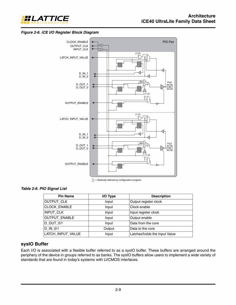
Figure 2-6. iCE I/O Register Block Diagram
Table 2-6. PIO Signal List
sysIO BufferEach I/O is associated with a flexible buffer referred to as a sysIO buffer. These buffers are arranged around the periphery of the device in groups referred to as banks. The sysIO buffers allow users to implement a wide variety of standards that are found in today’s systems with LVCMOS interfaces.
Pin Name I/O Type Description
OUTPUT_CLK Input Output register clock
CLOCK_ENABLE Input Clock enable
INPUT_CLK Input Input register clock
OUTPUT_ENABLE Input Output enable
D_OUT_0/1 Input Data from the core
D_IN_0/1 Output Data to the core
LATCH_INPUT_VALUE Input Latches/holds the Input Value
(1,0)
(1,0)
(1,0)01
(1,0)
Pad
Pad
CLOCK_ENABLE
OUTPUT_ENABLE
OUTPUT_ENABLE
OUTPUT_CLKINPUT_CLK
LATCH_INPUT_VALUE
LATCH_INPUT_VALUE
D_IN_1D_IN_0
D_OUT_1D_OUT_0
D_IN_1D_IN_0
D_OUT_1D_OUT_0
PIO Pair
01
= Statically defined by configuration program.

2-10
ArchitectureiCE40 UltraLite Family Data Sheet
Typical I/O Behavior During Power-upThe internal power-on-reset (POR) signal is deactivated when VCC, SPI_VCCIO, and VPP_2V5 reach the level defined in the Power-On-Reset Voltage table in the DC and Switching Characteristics chapter of this data sheet. After the POR signal is deactivated, the FPGA core logic becomes active. You must ensure that all VCCIO banks are active with valid input logic levels to properly control the output logic states of all the I/O banks that are critical to the application. The default configuration of the I/O pins in a device prior to configuration is tri-stated with a weak pull-up to VCCIO. The I/O pins maintain the pre-configuration state until VCC, SPI_VCCIO, and VPP_2V5 reach the defined levels. The I/Os take on the software user-configured settings only after POR signal is deactivated and the device performs a proper download/configuration. Unused I/Os are automatically blocked and the pull-up termina-tion is disabled.
Supported StandardsThe iCE40 UltraLite sysIO buffer supports both single-ended input/output standards, and used as differential com-parators. The buffer supports the LVCMOS 1.8, 2.5, and 3.3 V standards. The buffer has individually configurable options for bus maintenance (weak pull-up or none).
Table 2-7 and Table 2-8 show the I/O standards (together with their supply and reference voltages) supported by the iCE40 UltraLite devices.
Programmable Pull Up ResistorsThe iCE40 UltraLite sysIO buffer can be configured with programmable pull up resistors on every I/O. The options are 3.3 kOhms, 6.8 kOhms, 10 kOhms or 100 kOhms (default). This feature is useful in supporting the I2C interface. The user can also use it for other purposes.
Differential ComparatorsThe iCE40 UltraLite devices provide differential comparator on pairs of I/O pins. These comparators are useful in some mobile applications. Please refer to the Pin Information Summary section to locate the corresponding paired I/Os with differential comparators.
Table 2-7. Supported Input Standards
Table 2-8. Supported Output Standards
Input StandardVCCIO (Typical)
3.3 V 2.5 V 1.8 V
Single-Ended Interfaces
LVCMOS33 Yes
LVCMOS25 Yes
LVCMOS181 Yes
1. Not supported in bank 0 for 16-WLCP package.
Output Standard VCCIO (Typical)
Single-Ended Interfaces
LVCMOS33 3.3 V
LVCMOS25 2.5 V
LVCMOS181 1.8 V
1. Not supported in bank 0 for 16-WLCP package.
2-11
ArchitectureiCE40 UltraLite Family Data Sheet
On-Chip OscillatorThe iCE40 UltraLite devices feature two different frequency Oscillator. One is tailored for low-power operation that runs at low frequency (LFOSC). Both Oscillators are controlled with internally generated current.
The LFOSC runs at nominal frequency of 10 kHz. The high frequency oscillator (HFOSC) runs at a nominal fre-quency of 48 MHz, divisible to 24 MHz, 12 MHz, or 6 MHz, by user option. The LFOSC can be used to perform all always-on functions, with the lowest power possible. The HFOSC can be enabled when the always-on functions detect a condition that would need to wake up the system to perform higher frequency functions.
User I2C IPThe iCE40 UltraLite devices have two I2C IP cores. Either of the two cores can be configured either as an I2C mas-ter or as an I2C slave. The pins for the I2C interface are not pre-assigned. User can use any General Purpose I/O pins.
In each of the two cores, there are options to delay the either the input or the output, or both, by 50 ns nominal, using dedicated on-chip delay elements. This provides an easier interface with any external I2C components.
In optional FIFO mode, FIFOs are used for storing multiple bytes of data for transmit and / or receive in order to effi-ciently support the I2C sensor applications
When the IP core is configured as master, it will be able to control other devices on the I2C bus through the pre-assigned pin interface. When the core is configured as the slave, the device will be able to provide I/O expansion to an I2C Master. The I2C cores support the following functionality:
• Master and Slave operation
• 7-bit and 10-bit addressing
• Multi-master arbitration support
• Clock stretching
• Up to 1 MHz data transfer speed
• General Call support
• Optionally delaying input or output data, or both
• Optional FIFO mode
• Transmit FIFO size is 10 bits x 16 bytes, receive FIFO size is 10 bits x 32 bytes
For further information on the User I2C, please refer to TN1274, iCE40 SPI/I2C Hardened IP Usage Guide.
High Current LED Drive I/O PinsThe iCE40 UltraLite family devices offer multiple high current LED drive outputs in each device in the family to allow the iCE40 UltraLite product to drive LED signals directly on mobile applications.
There are three outputs on each device that can sink up to 24 mA current. These outputs are open-drain outputs, and provides sinking current to an LED connecting to the positive supply. These three outputs are designed to drive the RBG LEDs, such as the service LED found in a lot of mobile devices. An embedded RGB PWM IP is also offered in the family. This RGB drive current is user programmable from 4 mA to 24 mA, in increments of 4 mA in full current mode or from 2 mA to 12 mA, in increments of 2 mA in half current mode. This output functions as Gen-eral Purpose I/O with open-drain when the high current drive is not needed.
There is one output on each device that can sink up to 100 mA current. This output is open-drain, and provides sinking current to drive an external Barcode LED connecting to the positive supply. This Barcode drive current is user programmable from 16.6 mA to100 mA in increments of 16.6 mA in full current mode or 8.3 mA to 50 mA in

2-12
ArchitectureiCE40 UltraLite Family Data Sheet
increments of 8.3 mA in half current mode. This output functions as General Purpose I/O with open drain when the high current drive is not needed.
There is one output on each device that can sink up to 400 mA current. This output is open-drain, and provides sinking current to drive an external IR LED connecting to the positive supply. This IR drive current is user program-mable from 50 mA to 400 mA in increments of 50 mA in full current mode or from 25mA to 200mA in increments of 25mA in half current mode. This output functions as General Purpose I/O with open-drain when the high current drive is not needed. This output pin can also bond together with the Barcode output to drive higher current for IR LED.
The 400 mA IR LED drive output and the 100 mA Barcode LED drive output can be connected together to drive up to 500 mA IR LED, if higher than 400 mA driving capability is needed.
Table 2-9 shows the different LED driving current in the different selected Current Modes. IR500 LED applies with both IR LED and Barcode LED pins connected together.
Table 2-9. Current Drive
Hardened RGB PWM IPTo provide an easier usage of the RGB high current drivers to drive RGB LED, a Pulse-Width Modulator IP can be embedded into the user design. This PWM IP provides the flexibility for user to dynamically change the settings on the ON-time duration, OFF-time duration, and ability to turn the LED lights on and off gradually with user set breath-on and breath-off time.
For additional information on the PWM IP, please refer to TN1288, iCE40 LED Driver Usage Guide.
Hardened IR Transceiver IPThe IR Transceiver hard IP provides logic function to transmit and receive data through the Infrared LED data link. It takes the data residing inside the FPGA fabric to transmit with user specified frequency. In user enabled learning mode, it receives data from Infrared receiver and send the received data back to the FPGA fabric along with the measured receiving frequency.
For additional information on IR Transceiver IP, please see TN1288, iCE40 LED Driver Usage Guide.
Non-Volatile Configuration MemoryAll iCE40 UltraLite devices provide a Non-Volatile Configuration Memory (NVCM) block which can be used to con-figure the device.
For more information on the NVCM, please refer to TN1248, iCE40 Programming and Configuration.
Power On ResetiCE40 UltraLite devices have power-on reset circuitry to monitor VCC, SPI_VCCIO1, and VPP_2V5 voltage levels during power-up and operation. At power-up, the POR circuitry monitors these voltage levels. It then triggers
Full Current Mode Half Current Mode
mA (VCCIO= 3.3 V) mA (VCCIO=2.5 V) mA (VCCIO= 3.3 V) mA (VCCIO=2.5 V)
RGB LED 0, 4, 8, 12, 16, 20, 24 not allowed 0, 2, 4, 6, 8, 10, 12 0, 2, 4, 6, 8, 10, 12
BARCODE LED 0, 16.6, 33.3, 50, 66.6, 83.3, 100
not allowed 0, 8.3, 16.6, 25, 33.3, 41.6, 50
not allowed
IR400 LED 0, 50, 100, 150, 200, 250, 300, 350, 400
not allowed 0, 25, 50, 75, 100, 125, 150, 175, 200
0, 25, 50, 75, 100, 125, 150, 175, 200
IR500 LED 0, 50, 100, 150, 200, 250, 300, 350, 400, 450, 500
not allowed 0, 25, 50, 75, 100, 125, 150, 175, 200, 225, 250
0,25, 50, 75, 100, 125, 150, 175, 200, 225, 250

2-13
ArchitectureiCE40 UltraLite Family Data Sheet
download from either the internal NVCM or the external Flash memory after reaching the power-up levels speci-fied in the Power-On-Reset Voltage table in the DC and Switching Characteristics section of this data sheet. All power supplies should be powered up during configuration. Before and during configuration, the I/Os are held in tri-state. I/Os are released to user functionality once the device has finished configuration.
2-14
ArchitectureiCE40 UltraLite Family Data Sheet
iCE40 UltraLite Programming and ConfigurationThis section describes the programming and configuration of the iCE40 UltraLite family.
Device ProgrammingThe NVCM memory can be programmed through the SPI port. The SPI port is located in Bank 1, using SPI_VCCIO01 power supply.
Device ConfigurationThere are various ways to configure the Configuration RAM (CRAM), using SPI port, including:
• From a SPI Flash (Master SPI mode)
• System microprocessor to drive a Serial Slave SPI port (SSPI mode)
For more details on configuring the iCE40 UltraLite, please see TN1248, iCE40 Programming and Configuration.
Power Saving OptionsThe iCE40 UltraLite devices feature iCEGate and PLL low power mode to allow users to meet the static and dynamic power requirements of their applications. Table 2-10 describes the function of these features.
Table 2-10. iCE40 UltraLite Power Saving Features Description
Device Subsystem Feature Description
PLL When LATCHINPUTVALUE is enabled, puts the PLL into low-power mode; PLL output held static at last input clock value.
iCEGateTo save power, the optional iCEGate latch can selectively freeze the state of individual, non-regis-tered inputs within an I/O bank. Registered inputs are effectively frozen by their associated clock or clock-enable control.

www.latticesemi.com 3-1 DS1050 DC and Switching_01.4
November 2016 Data Sheet DS1050
© 2016 Lattice Semiconductor Corp. All Lattice trademarks, registered trademarks, patents, and disclaimers are as listed at www.latticesemi.com/legal. All other brand or product names are trademarks or registered trademarks of their respective holders. The specifications and information herein are subject to change without notice.
Absolute Maximum Ratings1, 2, 3
Supply Voltage VCC . . . . . . . . . . . . . . . . . . . . . . . . . . . . . . . . . . . . . . . . . . . . . . . . . . . . . . . . . . –0.5 V to 1.42 V
Output Supply Voltage VCCIO . . . . . . . . . . . . . . . . . . . . . . . . . . . . . . . . . . . . . . . . . . . . . . . . . . –0.5 V to 3.60 V
NVCM Supply Voltage VPP_2V5 . . . . . . . . . . . . . . . . . . . . . . . . . . . . . . . . . . . . . . . . . . . . . . . . . –0.5 V to 3.60 V
PLL Supply Voltage VCCPLL . . . . . . . . . . . . . . . . . . . . . . . . . . . . . . . . . . . . . . . . . . . . . . . . . . . . –0.5 V to 1.30 V
I/O Tri-state Voltage Applied. . . . . . . . . . . . . . . . . . . . . . . . . . . . . . . . . . . . . . . . . . . . . . . . . . . . –0.5 V to 3.60 V
Dedicated Input Voltage Applied . . . . . . . . . . . . . . . . . . . . . . . . . . . . . . . . . . . . . . . . . . . . . . . . –0.5 V to 3.60 V
Storage Temperature (Ambient). . . . . . . . . . . . . . . . . . . . . . . . . . . . . . . . . . . . . . . . . . . . . . . . . –65 °C to 150 °C
Junction Temperature (TJ) . . . . . . . . . . . . . . . . . . . . . . . . . . . . . . . . . . . . . . . . . . . . . . . . . . . . . –65 °C to 125 °C
1. Stress above those listed under the “Absolute Maximum Ratings” may cause permanent damage to the device. Functional operation of the device at these or any other conditions above those indicated in the operational sections of this specification is not implied.
2. Compliance with the Lattice Thermal Management document is required.3. All voltages referenced to GND.
iCE40 UltraLite Family Data SheetDC and Switching Characteristics

3-2
DC and Switching CharacteristicsiCE40 UltraLite Family Data Sheet
Recommended Operating Conditions1
Power Supply Ramp Rates1, 2
Power-On ResetAll iCE40 UltraLite devices have on-chip Power-On-Reset (POR) circuitry to ensure proper initialization of the device. Only three supply rails are monitored by the POR circuitry as follows: (1) VCC, (2) SPI_VCCIO1 and (3) VPP_2V5. All other supply pins have no effect on the power-on reset feature of the device. Note that all supply volt-age pins must be connected to power supplies for normal operation (including device configuration).
Power-Up Supply SequencingIt is recommended to bring up the power supplies in the following order. Note that there is no specified timing delay between the power supplies, however, there is a requirement for each supply to reach a level of 0.5V, or higher, before any subsequent power supplies in the sequence are applied.
1. VCC and VCCPLL should be the first two supplies to be applied. Note that these two supplies can be tied together subject to the recommendation to include a RC-based noise filter on the VCCPLL (Please refer to TN1252, iCE40 Hardware Checklist.)
2. SPI_VCCIO1 should be the next supply, and can be applied any time after the previous supplies (VCC and VCCPLL) have reached as level of 0.5 V or higher.
3. VPP_2V5 should be the next supply, and can be applied any time after previous supplies (VCC, VCCPLL and SPI_VCCIO1) have reached a level of 0.5 V or higher.
4. Other Supplies (VCCIO0 and VCCIO2) do not affect device power-up functionality, and they can be applied any time after the initial power supplies (VCC and VCCPLL) have reached a level of 0.5 V or greater. On the 16
Symbol Parameter Min. Max. Units
VCC1 Core Supply Voltage 1.14 1.26 V
VPP_2V5VPP_2V5 NVCM Programming and
Operating Supply Voltage
Slave SPI Configuration 1.714 3.46 V
Master SPI Configuration 2.30 3.46 V
Configuration from NVCM 2.30 3.46 V
NVCM Programming 2.30 3.00 V
VCCIO1, 2, 3 I/O Driver Supply Voltage VCCIO_0, SPI_VCCIO1, VCCIO_2 1.71 3.46 V
VCCPLL PLL Supply Voltage 1.14 1.26 V
tJCOM Junction Temperature Commercial Operation 0 85 °C
tJIND Junction Temperature Industrial Operation –40 100 °C
tPROG Junction Temperature NVCM Programming 10 30 °C
1. Like power supplies must be tied together if they are at the same supply voltage and they meet the power up sequence requirement. Please refer to Power-Up Supply Sequencing section. VCC and VCCPLL are recommended to tie to same supply with an RC-based noise filter between them. Please refer to TN1252, iCE40 Hardware Checklist.
2. See recommended voltages by I/O standard in subsequent table.3. VCCIO pins of unused I/O banks should be connected to the VCC power supply on boards.4. VPP_2V5 can, optionally, be connected to a 1.8 V (+/-5%) power supply in Slave SPI Configuration mode subject to the condition that none of
the HFOSC/LFOSC and RGB LED / IR / Barcode LED driver features are used. Otherwise, VPP_2V5 must be connected to a power supply with a minimum 2.30 V level.
Symbol Parameter Min. Max. Units
tRAMP Power supply ramp rates for all power supplies. 0.6 10 V/ms
1. Assumes monotonic ramp rates.2. Power-up sequence must be followed. Please refer to Power-Up Supply Sequencing section.

3-3
DC and Switching CharacteristicsiCE40 UltraLite Family Data Sheet
WLCSP package, VCCIO0 and VPP_2V5 are connected to the same pin on the package, and should be pow-ered as VPP_2V5 in the sequence.
There is no power down sequence required. However, when partial power supplies are powered down, it is required the above sequence to be followed when these supplies are repowered up again.
External ResetWhen all power supplies have reached to their minimum operating voltage defined in Minimum Operation Condition Table, it is required to either keep CRESET_B LOW, or toggle CRESET_B from HIGH to LOW, for a duration of tCRESET_B, and release it to go HIGH, to start configuration download from either the internal NVCM or the external Flash memory.
Figure 3-1 shows Power-Up sequence when SPI_VCCIO1 and VPP_2V5 are connected separately, and the CRESET_B signal triggers configuration download. Figure 3-2 shows when SPI_VCCIO1 and VPP_2V5 connected together. If the supply sequence is not followed, extra peak current may be observed on the supplies during power up.
All power supplies should be powered up during configuration. Before and during configuration, the I/Os are held in tri-state. I/Os are released to user functionality once the device has finished configuration.
Figure 3-1. Power Up Sequence with SPI_VCCIO1 and VPP_2V5 Not Connected Together
Figure 3-2. Power Up Sequence with All Supplies Connected Together
VCC/VCC_PLL = 1.2 V
SPI_VCCIO1 = 1.8 V
VPP_2V5, VCCIO0 and VCCIO2= 2.5 V / 3.3 V
0.5 V
CRESET_B
tCRESET_B
VSUPPLY(MIN)
VCC/VCC_PLL = 1.2 V
SPI_VCCIO, VPP_2V5, VCCIO0 and VCCIO2= 1.8 V / 2.5 V / 3.3 V
0.5 V
VSUPPLY(MIN)
CRESET_B tCRESET_B

3-4
DC and Switching CharacteristicsiCE40 UltraLite Family Data Sheet
Power-On-Reset Voltage Levels1
ESD PerformancePlease contact Lattice Semiconductor for additional information.
DC Electrical CharacteristicsOver Recommended Operating Conditions
Symbol Parameter Min. Max. Units
VPORUPPower-On-Reset ramp-up trip point (circuit monitoring VCC, SPI_VCCIO1, VPP_2V5)
VCC 0.6 1 V
SPI_VCCIO1 0.7 1.6 V
VPP_2V5 0.7 1.6 V
VPORDNPower-On-Reset ramp-down trip point (circuit monitor-ing VCC, SPI_VCCIO1, VPP_2V5)
VCC — 0.85 V
SPI_VCCIO1 — 1.6 V
VPP_2V5 — 1.6 V
1. These POR trip points are only provided for guidance. Device operation is only characterized for power supply voltages specified under rec-ommended operating conditions.
Symbol Parameter Condition Min. Typ. Max. Units
IIL, IIH1, 3, 4 Input or I/O Leakage 0V < VIN < VCCIO + 0.2 V — — +/–10 µA
C1 I/O Capacitance2 VCCIO = 3.3 V, 2.5 V, 1.8 VVCC = Typ., VIO = 0 to VCCIO + 0.2 V — 6 — pf
C2Global Input Buffer Capacitance2
VCCIO = 3.3 V, 2.5 V, 1.8 VVCC = Typ., VIO = 0 to VCCIO + 0.2 V — 6 — pf
C3 24 mA LED I/O Capacitance VCCIO = 3.3 V, 2.5 V, 1.8 VVCC = Typ., VIO = 0 to VCCIO + 0.2 V — 20 — pf
C4 400 mA LED I/O Capacitance VCCIO = 3.3 V, 2.5 V, 1.8 VVCC = Typ., VIO = 0 to VCCIO + 0.2 V — 53 — pf
C5 100 mA LED I/O Capacitance VCCIO = 3.3 V, 2.5 V, 1.8 VVCC = Typ., VIO = 0 to VCCIO + 0.2 V — 20 — pf
VHYST Input Hysteresis VCCIO = 1.8 V, 2.5 V, 3.3 V — 200 — mV
IPUInternal PIO Pull-up Current
VCCIO = 1.8 V, 0=<VIN<=0.65 VCCIO –3 — –31 µA
VCCIO = 2.5 V, 0=<VIN<=0.65 VCCIO –8 — –72 µA
VCCIO = 3.3 V, 0=<VIN<=0.65 VCCIO –11 — –128 µA
1. Input or I/O leakage current is measured with the pin configured as an input or as an I/O with the output driver tri-stated. It is not measured with the output driver active. Internal pull-up resistors are disabled.
2. TJ 25°C, f = 1.0 MHz.3. Please refer to VIL and VIH in the sysIO Single-Ended DC Electrical Characteristics table of this document.4. Input pins are clamped to VCCIO and GND by a diode. When input is higher than VCCIO or lower than GND, the Input Leakage current will be
higher than the IIL and IIH.

3-5
DC and Switching CharacteristicsiCE40 UltraLite Family Data Sheet
Supply Current 1, 2, 3, 4, 5
Internal Pull-Up Resistor Specifications
User I2C Specifications1
Symbol ParameterTyp. VCC =
1.2 V4 Units
ICCSTDBY Core Power Supply Static Current 35 µA
IPP2V5STDBY VPP_2V5 Power Supply Static Current 1 µA
ICCPLLSTDBY PLL Power Supply Static Current 1 µA
ICCIOSTDBY VCCIO Power Supply Static Current 1 at VCCIO equal or less 2.5 V; 5 at VCCIO equal
or less 3.465 V
µA
ICCPEAK Core Power Supply Startup Peak Current 3.06 mA
IPP_2V5PEAK VPP_2V5 Power Supply Startup Peak Current 2.15 mA
ICCPLLPEAK PLL Power Supply Startup Peak Current 3.066 mA
ICCIOPEAK VCCIO Power Supply Startup Peak Current 4.65 for config bank, 0.25 for regular IO bank
mA
1. Assumes programmed pattern with the following characteristics: all outputs are tri-stated, all inputs are configured as LVCMOS and held at VCCIO or GND, on-chip PLL is off. For more detail with your specific design, use the Power Calculator tool. Power specified with master SPI configuration mode. Other modes may be up to 25% higher.
2. Frequency = 0 MHz.3. TJ = 25 °C, power supplies at nominal voltage.4. Does not include pull-up.5. Peak current is the in rush current - highest current during power supply start up within the power supply ramp rate. See Power Supply
Ramp Rates1, 2 section. These currents are measured with decoupling capacitance of 0.1 uF, 10 nF, and 1 nF to the power supply. Higher decoupling capacitance causes higher current.
6. PLL power supply shared with Core Power supply.
Parameter Condition Spec Units
Min Typ Max
Resistor_3.3K 1.71 < Vccio < 3.47 V 2.64 3.3 3.96 kOhm
Resistor_6.8K 1.71 < Vccio < 3.47 V 5.44 6.8 8.16 kOhm
Resistor_10K 1.71 < Vccio < 3.47 V 8 10 12 kOhm
Weak pull-up resistor
1.71 < Vccio < 1.89 V — 100 — kOhm
2.38 < Vccio < 2.63 V — 55 — kOhm
3.13 < Vccio < 3.47 V — 40 — kOhm
SN Symbol Parameter STD Mode FAST Mode FAST Mode Plus
Min Max Min Max Min Max Units
1 fSCL SCL clock frequency 100 400 10002 kHz
1. Refer to the I2C specification for timing requirements.2. Fast Mode Plus maximum speed may be achieved by using external pull up resistor on I2C bus. Internal pull up may not be sufficient to sup-
port the maximum speed.

3-6
DC and Switching CharacteristicsiCE40 UltraLite Family Data Sheet
Internal Oscillators (HFOSC, LFOSC)
sysIO Recommended Operating Conditions
sysIO Single-Ended DC Electrical Characteristics
Differential Comparator Electrical Characteristics
Derating Logic TimingLogic timing provided in the following sections of the data sheet and the Lattice design tools are worst case num-bers in the operating range. Actual delays may be much faster. Lattice design tools can provide logic timing num-bers at a particular temperature and voltage.
Parameter Parameter Description Spec/Recommended Units
Symbol Conditions Min Typ Max
fCLKHFCommercial Temp HFOSC clock frequency (tJ = 0 oC–85 oC) –10% 48 10% MHz
Industrial Temp HFOSC clock frequency (tJ = –40 oC–100 oC) –20% 48 20% MHz
fCLKLF LFOSC CLKK clock frequency –10% 10 10% kHz
DCHCLKHFCommercial Temp HFOSC clock frequency (tJ = 0 oC–85 oC) 45 50 55 %
Industrial Temp HFOSC clock frequency (tJ = –45 oC–100 oC) 40 50 60 %
DCHCLKLF LFOSC Duty Cycle (Clock High Period) 45 50 55 %
tWAKEUP Delay OSC Enable to output enable delay — — 100 µs
Tsync_on Oscillator output synchronizer delay — — 5 Cycles
Tsync_off Oscillator output disable delay — — 5 Cycles
Standard
VCCIO (V)
Min. Typ. Max.
LVCMOS 3.3 3.14 3.3 3.46
LVCMOS 2.5 2.37 2.5 2.62
LVCMOS 1.8 1.71 1.8 1.89
Input/Output
Standard
VIL VIHVOL Max.
(V)VOH Min.
(V)IOL Max.
(mA)IOH Max.
(mA)Min. (V) Max. (V) Min. (V) Max. (V)
LVCMOS 3.3 -0.3 0.8 2.0 VCCIO + 0.2V0.4 VCCIO - 0.4 8 –8
0.2 VCCIO - 0.2 0.1 –0.1
LVCMOS 2.5 -0.3 0.7 1.7 VCCIO + 0.2V0.4 VCCIO - 0.4 6 –6
0.2 VCCIO - 0.2 0.1 –0.1
LVCMOS 1.8 -0.3 0.35VCCIO 0.65VCCIO VCCIO + 0.2V0.4 VCCIO - 0.4 4 –4
0.2 VCCIO - 0.2 0.1 –0.1
Parameter Symbol Parameter Description
Test Conditions Min. Max. Units
VREF Reference Voltage to compare, on VINM VCCIO = 2.5 V 0.25 VCCIO –0.25 V V
VDIFFIN_H Differential input HIGH (VINP - VINM) VCCIO = 2.5 V 250 — mV
VDIFFIN_L Differential input LOW (VINP - VINM) VCCIO = 2.5 V — –250 mV
IIN Input Current, VINP and VINM VCCIO = 2.5 V –10 10 µA

3-7
DC and Switching CharacteristicsiCE40 UltraLite Family Data Sheet
Maximum sysIO Buffer Performance1
iCE40 UltraLite External Switching CharacteristicsOver Recommended Operating Conditions
I/O Standard Max. Speed Units
Inputs
LVCMOS33 250 MHz
LVCMOS25 250 MHz
LVCMOS18 250 MHz
LED I/O used as GPIO open drain 50 MHz
Outputs
LVCMOS33 250 MHz
LVCMOS25 250 MHz
LVCMOS18 155 MHz
LED I/O used as GPIO open drain 502 MHz
1. Measured with a toggling pattern.2. With external resistor from 180 Ohm to 250 Ohm and capacity of no more than 15 pF.
Parameter Description Device Min Max Units
Global Clocks
fMAX_GBUF Frequency for Global Buffer Clock network All devices — 185 MHz
tW_GBUF Clock Pulse Width for Global Buffer All devices 2 — ns
tSKEW_GBUF Global Buffer Clock Skew Within a Device All devices — 500 ps
Pin-LUT-Pin Propagation Delay
tPDBest case propagation delay through one LUT logic All devices — 9.0 ns
General I/O Pin Parameters (Using Global Buffer Clock without PLL)1
tSKEW_IO Data bus skew across a bank of IOs All devices — 410 ps
tCO Clock to Output - PIO Output Register All devices — 9.0 ns
tSU Clock to Data Setup - PIO Input Register All devices –0.5 — ns
tH Clock to Data Hold - PIO Input Register All devices 5.55 — ns
General I/O Pin Parameters (Using Global Buffer Clock with PLL)
tCOPLL Clock to Output - PIO Output Register All Devices — 2.9 ns
tSUPLL Clock to Data Setup - PIO Input Register All Devices 7.9 — ns
tHPLL Clock to Data Hold - PIO Input Register All Devices –0.6 — ns
1. All the data is from the worst case condition.

3-8
DC and Switching CharacteristicsiCE40 UltraLite Family Data Sheet
sysCLOCK PLL TimingOver Recommended Operating Conditions
SPI Master or NVCM Configuration Time1, 2
Parameter Descriptions Conditions Min. Max. Units
fINInput Clock Frequency (REFERENCECLK, EXTFEEDBACK) 10 133 MHz
fOUT Output Clock Frequency (PLLOUT) 16 275 MHz
fVCO PLL VCO Frequency 533 1066 MHz
fPFD Phase Detector Input Frequency 10 133 MHz
AC Characteristics
tDT Output Clock Duty Cycle 40 60 %
tPH Output Phase Accuracy — +/–12 deg
tOPJIT1, 5
Output Clock Period JitterfOUT >= 100 MHz — 450 ps p-p
fOUT < 100 MHz — 0.05 UIPP
Output Clock Cycle-to-cycle JitterfOUT >= 100 MHz — 750 ps p-p
fOUT < 100 MHz — 0.10 UIPP
Output Clock Phase JitterfPFD >= 25 MHz — 275 ps p-p
fPFD < 25 MHz — 0.05 UIPP
tW Output Clock Pulse Width At 90% or 10% 1.33 — ns
tLOCK2, 3 PLL Lock-in Time — 50 µs
tUNLOCK PLL Unlock Time — 50 ns
tIPJIT4 Input Clock Period Jitter
fPFD 20 MHz — 1000 ps p-p
fPFD < 20 MHz — 0.02 UIPP
tSTABLE3 LATCHINPUTVALUE LOW to PLL Stable — 500 ns
tSTABLE_PW3 LATCHINPUTVALUE Pulse Width 100 — ns
tRST RESET Pulse Width 10 — ns
tRSTREC RESET Recovery Time 10 — µs
tDYNAMIC_WD DYNAMICDELAY Pulse Width 100 — VCO Cycles
1. Period jitter sample is taken over 10,000 samples of the primary PLL output with a clean reference clock. Cycle-to-cycle jitter is taken over 1000 cycles. Phase jitter is taken over 2000 cycles. All values per JESD65B.
2. Output clock is valid after tLOCK for PLL reset and dynamic delay adjustment.3. At minimum fPFD. As the fPFD increases the time will decrease to approximately 60% the value listed.4. Maximum limit to prevent PLL unlock from occurring. Does not imply the PLL will operate within the output specifications listed in this table.5. The jitter values will increase with loading of the PLD fabric and in the presence of SSO noise.
Symbol Parameter Conditions Max. Units
tCONFIG POR/CRESET_B to Device I/O Active
All devices - Low Frequency (Default) 53 ms
All devices - Medium frequency 25 ms
All devices - High frequency 13 ms
1. Assumes sysMEM Block is initialized to an all zero pattern if they are used.2. The NVCM download time is measured with a fast ramp rate starting from the maximum voltage of POR trip point.

3-9
DC and Switching CharacteristicsiCE40 UltraLite Family Data Sheet
sysCONFIG Port Timing SpecificationsSymbol Parameter Conditions Min. Typ. Max. Units
All Configuration Modes
tCRESET_B
Minimum CRESET_B LOW pulse width required to restart configuration, from falling edge to rising edge
200 — — ns
tDONE_IO
Number of configuration clock cycles after CDONE goes HIGH before the PIO pins are activated
49 — — Clock Cycles
Slave SPI
tCR_SCK
Minimum time from a rising edge on CRESET_B until the first SPI WRITE operation, first SPI_XCK clock. During this time, the iCE40 UltraLite device is clearing its internal configuration mem-ory
1200 — — µs
fMAX CCLK clock frequencyWrite 1 — 25 MHz
Read1 — 15 — MHz
tCCLKH CCLK clock pulsewidth HIGH 20 — — ns
tCCLKL CCLK clock pulsewidth LOW 20 — — ns
tSTSU CCLK setup time 12 — — ns
tSTH CCLK hold time 12 — — ns
tSTCO CCLK falling edge to valid output 13 — — ns
Master SPI3
fMCLK MCLK clock frequency
Low Frequency (Default)
7.0 12.0 17.0 MHz
Medium Frequency2 21.0 33.0 45.0 MHz
High Frequency2 33.0 53.0 71.0 MHz
tMCLK CRESET_B HIGH to first MCLK edge 1200 — — µs
tMTSU MCLK setup time4 9.9 — — ns
tMTH MCLK hold time 1 — — ns
1. Supported with 1.2 V Vcc and at 25 C.2. Extended range fMAX Write operations support up to 53 MHz with 1.2 V VCC and at 25 C.3. tSU and tHD timing must be met for all MCLK frequency choices4. For considerations of SPI Master Configuration Mode, please refer to TN1248, iCE40 Programming and Configuration.
3-10
DC and Switching CharacteristicsiCE40 UltraLite Family Data Sheet
High Current LED, IR LED and Barcode LED Drives1
RGB LED Timing Specification
IR Transceiver IP Timing Specification
Symbol Parameter VCCIO = 3.3 V VCCIO = 2.5 V
Min. Max. Units Min. Max. Units
IRGB_ACCURACY_FULL RGB LED0, LED1, LED2 Sink Cur-rent Accuracy to selected current @ VPAD = 0.5 ~ 2.5 V
–12 +12 % not allowed
not allowed
%
IRGB_ACCURACY_HALF RGB LED0, LED1, LED2 Sink Cur-rent Accuracy to selected current @ VPAD = 0.35 ~ 2.5 V
–14 +14 % –14 +14 %
IRGB_MATCH RGB LED0, LED1, LED2 Sink Cur-rent Matching among the 3 outputs @ VPAD = 0.35 ~ 2.5 V
–5 +5 % –5 +5 %
IIR_ACCURACY_FULL IR LED Sink Current Accuracy to selected current @ VPAD = 0.8 V ~ 2 V
–12 +12 % not allowed
not allowed
%
IIR_ACCURACY_HALF IR LED Sink Current Accuracy to selected current @ VPAD = 0.55 V ~ 2 V
–12 +12 % –12 +12 %
IBARCODE_ACCURACY_FULL BARCODE LED Sink Current Accuracy to selected current @ VPAD = 0.8 V ~ 2 V
–12 +12 % not allowed
not allowed
%
IBARCODE_ACCURACY_HALF BARCODE LED Sink Current Accuracy to selected current @ VPAD = 0.55 V ~ 2 V
–12 +12 % not allowed
not allowed
%
1. Refer to Table 2-9 for valid current settings.
SN Symbol Parameter Min TYP Max Units
1 FPWM_OUT_XFR250 = 0
Frequency of the PWM output for color LED; When FR250 = 0
125 Hz
2 FPWM_OUT_XFR250 = 1
Frequency of the PWM output for color LED; When FR250 = 1
250 Hz
3 THIGH_X PWM High percentage for color LED. 0 99 %
4 THIGH_STEP_X PWM High percentage incremental step. 1/256 %
SN Symbol Parameter Min TYP Max Units
1 FIR_OUT Frequency of the IR output 25 120 kHz
2 FIR_IN Frequency of the IR input 25 120 kHz
3 THIGH (DUTY1/3 = 0) Duty Cycle when DUTY1/3 = 0. 50 %
4 THIGH (DUTY1/3 = 1) Duty Cycle when DUTY1/3 = 1. 33.33 %
3-11
DC and Switching CharacteristicsiCE40 UltraLite Family Data Sheet
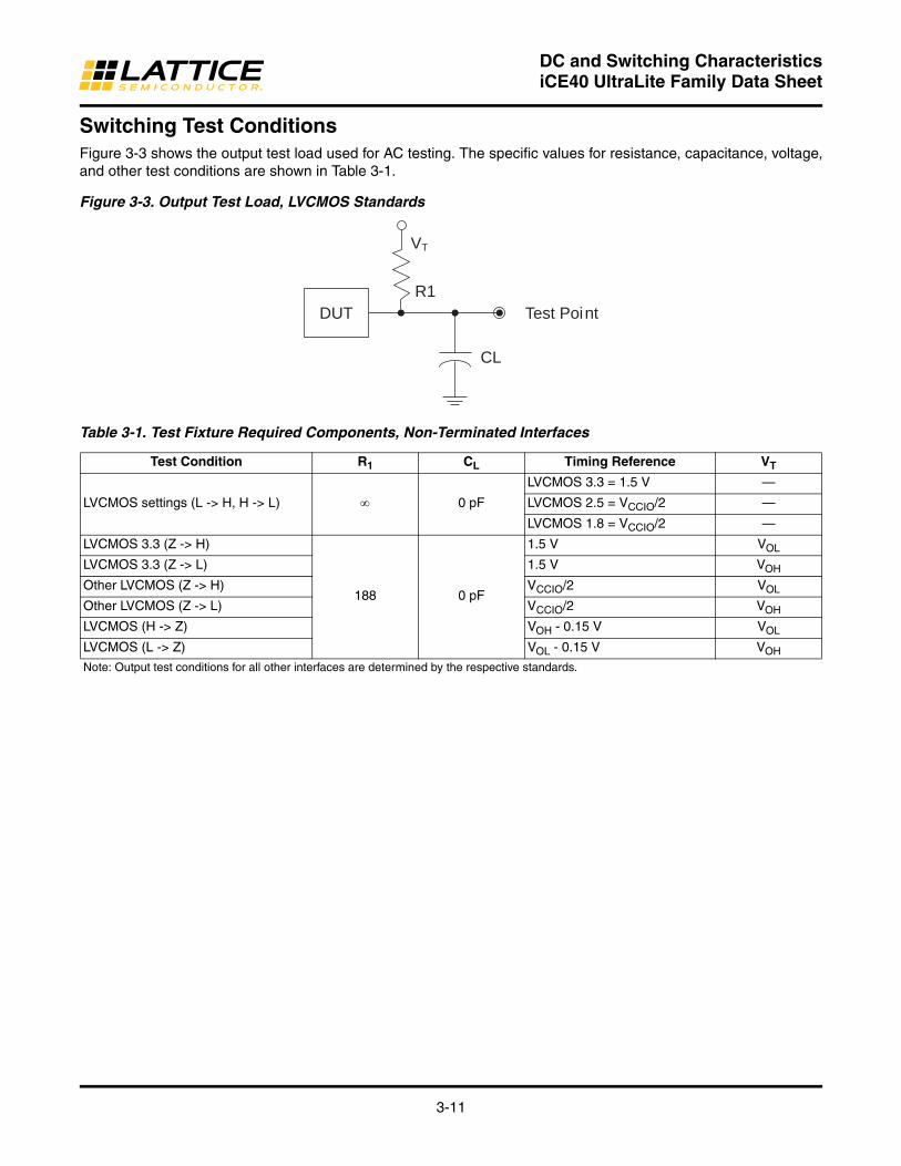
Switching Test ConditionsFigure 3-3 shows the output test load used for AC testing. The specific values for resistance, capacitance, voltage, and other test conditions are shown in Table 3-1.
Figure 3-3. Output Test Load, LVCMOS Standards
Table 3-1. Test Fixture Required Components, Non-Terminated Interfaces
Test Condition R1 CL Timing Reference VT
LVCMOS settings (L -> H, H -> L) 0 pF
LVCMOS 3.3 = 1.5 V —
LVCMOS 2.5 = VCCIO/2 —
LVCMOS 1.8 = VCCIO/2 —
LVCMOS 3.3 (Z -> H)
188 0 pF
1.5 V VOL
LVCMOS 3.3 (Z -> L) 1.5 V VOH
Other LVCMOS (Z -> H) VCCIO/2 VOL
Other LVCMOS (Z -> L) VCCIO/2 VOH
LVCMOS (H -> Z) VOH - 0.15 V VOL
LVCMOS (L -> Z) VOL - 0.15 V VOH
Note: Output test conditions for all other interfaces are determined by the respective standards.
DUT
V T
R1
CL
Test Poi n t

www.latticesemi.com 4-1 DS1050 Pinout Information_01.1
April 2016 Data Sheet DS1050
© 2016 Lattice Semiconductor Corp. All Lattice trademarks, registered trademarks, patents, and disclaimers are as listed at www.latticesemi.com/legal. All other brand or product names are trademarks or registered trademarks of their respective holders. The specifications and information herein are subject to change without notice.
Signal DescriptionsSignal Name Function I/O Description
Power Supplies
VCC Power — Core Power Supply
VCCIO_0, SPI_VCCIO1, VCCIO_2 Power — Power for I/Os in Bank 0, 1, and 2. VCCIO0 is tied with VPP_2V5 and VCCIO2 is tied with SPI_VCCIO1 in 16 WLCS package.
VPP_2V5 Power — Power for NVCM programming and operations
VCCPLL Power — Power for PLL
GND GROUND — Ground
GND_LED GROUND — Ground for LED drivers. Should connect to GND on board
Configuration
Primary Secondary
CRESETB — Configuration I Configuration Reset, active LOW. Include a weak internal pull-up resistor to VCCIO_2. Or actively driven externally or connect an 10K-Ohm pull-up to VCCIO_2.
PIOB_8a CDONE Configuration I/O Configuration Done. Includes a weak pull-up resistor to VCCIO_2. In 16 WLCS CDONE shared with PIOB_8a.
General I/O I/O In user mode, after configuration, this pin can be pro-grammed as general I/O in user function.
PIOB_11b CDONE Configuration I/O Configuration Done. Includes a weak pull-up resistor to VCCIO_2. In 36-ball ucBGA package CDONE shared with PIOB_11b.
General I/O I/O In user mode, after configuration, this pin can be pro-grammed as general I/O in user function.
Config SPI
Primary Secondary
PIOB_16a SPI_SCK Configuration I/O This pin is shared with device configuration. During configuration:In Master SPI mode, this pin outputs the clock to external SPI memory.In Slave SPI mode, this pin inputs the clock from external processor.
General I/O I/O In user mode, after configuration, this pin can be pro-grammed as general I/O in user function.
PIOB_14a SPI_SO Configuration Output This pin is shared with device configuration. During configuration:In Master SPI mode, this pin outputs the command data to external SPI memory.In Slave SPI mode, this pin connects to the MISO pin of the external processor.
General I/O I/O In user mode, after configuration, this pin can be pro-grammed as general I/O in user function.
iCE40 UltraLite Family Data SheetPinout Information

4-2
Pinout InformationiCE40 UltraLite Family Data Sheet
PIOB_15b SPI_SI Configuration Input This pin is shared with device configuration. During configuration:In Master SPI mode, this pin receives data from exter-nal SPI memory.In Slave SPI mode, this pin connects to the MOSI pin of the external processor.
General I/O I/O In user mode, after configuration, this pin can be pro-grammed as general I/O in user function
PIOB_17b SPI_SS_B Configuration I/O This pin is shared with device configuration. During configuration:In Master SPI mode, this pin outputs to the external SPI memory.In Slave SPI mode, this pin inputs from the external processor.
General I/O I/O In user mode, after configuration, this pin can be pro-grammed as general I/O in user function.
Global Signals
Primary Secondary
PIOT_22b G0 General I/O I/O In user mode, after configuration, this pin can be pro-grammed as general I/O in user function.
Global Input Global input used for high fanout, or clock/reset net. The G0 pin drives the GBUF0 global buffer.
PIOT_21a G1 General I/O I/O In user mode, after configuration, this pin can be pro-grammed as general I/O in user function.
Global Input Global input used for high fanout, or clock/reset net. The G1 pin drives the GBUF1 global buffer.
PIOB_13b G3 General I/O I/O In user mode, after configuration, this pin can be pro-grammed as general I/O in user function.
Global Input Global input used for high fanout, or clock/reset net. The G3 pin drives the GBUF3 global buffer.
PIOB_8a G4 General I/O I/O In user mode, after configuration, this pin can be pro-grammed as general I/O in user function.
Global Input Global input used for high fanout, or clock/reset net. The G4 pin drives the GBUF4 global buffer.
PIOB_7b G5 General I/O I/O In user mode, after configuration, this pin can be pro-grammed as general I/O in user function.
Global Input Global input used for high fanout, or clock/reset net. The G5 pin drives the GBUF5 global buffer.
PIOB_3b G6 General I/O I/O In user mode, after configuration, this pin can be pro-grammed as general I/O in user function.
Global Input Global input used for high fanout, or clock/reset net. The G6 pin drives the GBUF6 global buffer.
LED Signals
RGB0 General I/O Open-Drain I/O In user mode, with user's choice, this pin can be pro-grammed as open drain I/O in user function.
LED Open-Drain Output
In user mode, with user's choice, this pin can be pro-grammed as open drain 24mA output to drive exter-nal LED.
RGB1 General I/O Open-Drain I/O In user mode, with user's choice, this pin can be pro-grammed as open drain I/O in user function.
LED Open-Drain Output
In user mode, with user's choice, this pin can be pro-grammed as open drain 24mA output to drive exter-nal LED.

4-3
Pinout InformationiCE40 UltraLite Family Data Sheet
RGB2 General I/O Open-Drain I/O In user mode, with user's choice, this pin can be pro-grammed as open drain I/O in user function.
LED Open-Drain Output
In user mode, with user's choice, this pin can be pro-grammed as open drain 24mA output to drive exter-nal LED.
IRLED General I/O Open-Drain I/O In user mode, with user's choice, this pin can be pro-grammed as open drain I/O in user function.
LED Open-Drain Output
In user mode, with user's choice, this pin can be pro-grammed as open drain 400 mA output to drive exter-nal LED.
BARCODE General I/O Open-Drain I/O In user mode, with user's choice, this pin can be pro-grammed as open drain I/O in user function.
LED Open-Drain Output
In user mode, with user's choice, this pin can be pro-grammed as open drain 100 mA output to drive exter-nal LED.
PIOT_xx General I/O I/O In user mode, with user's choice, this pin can be pro-grammed as I/O in user function in the top (xx = I/O location).
PIOB_xx General I/O I/O In user mode, with user's choice, this pin can be pro-grammed as I/O in user function in the bottom (xx = I/O location).

4-4
Pinout InformationiCE40 UltraLite Family Data Sheet
Pin Information Summary
Pin TypeiCE40UL1K iCE40UL640
SWG16 36 ucBGA SWG16 36 ucBGA
General Purpose I/O Per Bank
Bank 0 5 12 5 12
Bank 1 4 4 4 4
Bank 2 1 10 1 10
Total General Purpose I/Os 10 26 10 26
VCC 1 1 1 1
VCCIO Bank 0 0 1 0 1
Bank 1 0 1 0 1
Bank 2 1 1 1 1
VCCPLL 0 1 0 1
VCPP_2V5 1 1 1 1
CRESET_B 1 1 1 1
CDONE 0 0 0 0
GND 1 2 1 2
GND_LED 1 1 1 1
Total Balls 16 36 16 36

www.latticesemi.com 5-1 DS1050 Order Info_01.1
April 2016 Data Sheet DS1050
© 2016 Lattice Semiconductor Corp. All Lattice trademarks, registered trademarks, patents, and disclaimers are as listed at www.latticesemi.com/legal. All other brand or product names are trademarks or registered trademarks of their respective holders. The specifications and information herein are subject to change without notice.
iCE40 UltraLite Part Number Description
Tape and Reel Quantity
Ordering Part NumbersIndustrial
Package TR Quantity
CM36A 4,000
SWG16 5,000
Part Number LUTs Supply Voltage Package Pins Temp.
ICE40UL1K-SWG16ITR 1248 1.2 Halogen-Free WLCSP 16 IND
ICE40UL1K-CM36AITR 1248 1.2 36-Ball ucBGA 36 IND
ICE40UL1K-CM36AITR1K 1248 1.2 36-Ball ucBGA 36 IND
ICE40UL640-SWG16ITR 640 1.2 Halogen-Free WLCSP 16 IND
ICE40UL640-CM36AITR 640 1.2 36-Ball ucBGA 36 IND
ICE40UL640-CM36AITR1K 640 1.2 36-Ball ucBGA 36 IND
Logic Cells
Package SWG16 = 16-Ball WLCSP (0.35 mm Ball Pitch) CM36A = 36-Ball ucBGA (0.40 mm Ball Pitch)
Device Family iCE40 UltraLite FPGA
iCE40ULXX-XXXXXITR
640 = 640 Logic Cells1K = 1,248 Logic Cells
Shipping Method Blank = Trays TR = Tape and Reel (See quantity below) TR1K = Tape and Reel, 1,000 units
Grade I = Industrial
iCE40 UltraLite Family Data SheetOrdering Information

July 2016 Data Sheet DS1050
© 2016 Lattice Semiconductor Corp. All Lattice trademarks, registered trademarks, patents, and disclaimers are as listed at www.latticesemi.com/legal. All other brand or product names are trademarks or registered trademarks of their respective holders. The specifications and information herein are subject to change without notice.
www.latticesemi.com 6-1 DS1050 Further Info_01.1
For Further InformationA variety of technical notes for the iCE40 UltraLite family are available on the Lattice web site.
• TN1248, iCE40 Programming and Configuration
• TN1274, iCE40 I2C and SPI Hardened IP Usage Guide
• TN1276, Advanced iCE40 I2C and SPI Hardened IP Usage Guide
• TN1250, Memory Usage Guide for iCE40 Devices
• TN1251, iCE40 sysCLOCK PLL Design and Usage Guide
• TN1252, iCE40 Hardware Checklist
• TN1288, iCE40 LED Driver Usage Guide
• iCE40 UltraLite Pinout Files
• iCE40 UltraLite Pin Migration Files
• Thermal Management document
• Lattice design tools
• Schematic Symbols
iCE40 UltraLite Family Data SheetSupplemental Information
November 2016 Data Sheet DS1050
© 2016 Lattice Semiconductor Corp. All Lattice trademarks, registered trademarks, patents, and disclaimers are as listed at www.latticesemi.com/legal. All other brand or product names are trademarks or registered trademarks of their respective holders. The specifications and information herein are subject to change without notice.
www.latticesemi.com 7-1 DS1050 Revision History
Date Version Section Change Summary
November 2016 1.4 DC and Switching Characteristics
Updated External Reset section. Added information on following supply sequence.
June 2016 1.3 Introduction Updated General Description section.— Changed “embedded RGB PWM IP” to ”hardened RGB PWM IP”.— Changed “modulation logic” to “hardened TX/RX pulse logic”.— Updated information on the use of 500 mA IR driver.
Updated Introduction section.— Added “RGB LED and IR LED” to configurable Controllers.— Added “LED” to RGB control functions.
Architecture Updated Architecture Overview section. — Changed caption to Figure 2-1, iCE40UL1K iCE40UL-1K Device, Top View.— Changed logic blocks to PLB.— Changed “LED sink” to “RGB and IR LED sinks, and a 100 mA Bar-code emulation output”.— Corrected headings in Table 2-2, Global Buffer (GBUF) Connections to Programmable Logic Blocks.— Updated footnote in Table 2-4, sysMEM Block Configuration.— Updated sysIO Buffer Banks section.— Corrected VCCIO format in Figure 2-5, I/O Bank and Programmable I/O Cell.— Updated Typical I/O Behavior During Power-up section.— Updated Supported Standards section.— Updated Programmable Pull Up Resistors section.— Changed “more than one byte” to “multiple bytes” in User I2C IP sec-tion.— Updated High Current LED Drive I/O Pins section.Changed heading to High Current LED Drive I/O Pins. Added LED to “high current drive”. Added information on use of 500 mA IR LED. Added paragraph to reference Table 2-9.— Changed heading to Hardened RGB PWM IP. — Changed heading to Hardened IR Transceiver IP.
Updated iCE40 UltraLite Programming and Configuration section. Changed VCCIO_1 to SPI_VCCIO1 in Device Programming.
DC and Switching Characteristics
Updated Absolute Maximum Ratings section. Corrected VPP_2V5 and VCCPLL format.
Updated Recommended Operating Conditions section. — Changed heading to Hardened RGB PWM IP. — Updated footnote.
Removed Power-up Sequence section.
Added the following sections:— Power-On Reset— Power-Up Supply Sequencing— External Reset
Updated DC Electrical Characteristics section. Revised footnote 4.
Updated Supply Current section. — Changed VPP_2V5 format. — Updated footnote 5.
Updated Internal Oscillators (HFOSC, LFOSC) section. Added Com-mercial and Industrial Temp values for fCLKHF and DCHCLKHF.
Updated Differential Comparator Electrical Characteristics section.
iCE40 UltraLite Family Data SheetRevision History

7-2
Revision HistoryiCE540 Ultra Family Data Sheet
Updated iCE40 UltraLite External Switching Characteristics section. Revised footnote.
Updated sysCLOCK PLL Timing section. Revised tOPJIT conditions.
Updated sysCONFIG Port Timing Specifications section. — Added footnote to Master SPI.— Added footnote to MCLK setup time.— Revised tMTSU minimum value.— Added footnotes 3 and 4.
Supplemental Information
Updated For Further Information section. Added reference to TN1252, iCE40 Hardware Checklist.
April 2016 1.2 Introduction Updated Features section.— Updated BGA package to ucBGA.— Corrected HF Oscillator unit in Table 1-1, iCE40 UltraLite Family Selection Guide.
Architecture Updated sysCLOCK Phase Locked Loops (PLLs) (sysCLOCK PLL is only supported in 36-ball ucBGA package) section. Updated BGA pack-age to ucBGA in heading.
DC and Switching Characteristics
Updated Recommended Operating Conditions section. Added footnote 4 regarding VPP_2V5.
Pinout Information Updated Signal Descriptions and Pin Information Summary sections. — Updated BGA package to ucBGA.— Changed SPI_CSN to SPI_SS_B.— Corrected minor typo errors.
Ordering Information Updated iCE40 UltraLite Part Number Description section.— Added shipment types.— Updated BGA package to ucBGA.
Added Tape and Reel Quantity section.
Updated Ordering Part Numbers section.— Added part numbers.— Updated BGA package to ucBGA.
March 2015 1.1 All Document status changed from Preliminary to Final.
Introduction Updated General Description and Features sections. Changed the LFOSC frequency value from 9.7 kHz to 10 kHz.
Architecture Updated On-Chip Oscillator section. Changed the LFOSC frequency value from 9.7 kHz to 10 kHz.
DC and Switching Characteristics
Updated Power-up Sequence section. Revised power-up sequence description for 16-ball WLCSP. Added Power-up Sequence table.
Updated User I2C Specifications section. Added footnote 2.
Updated Internal Oscillators (HFOSC, LFOSC) section. Added and revised values. Removed footnote.
Updated Maximum sysIO Buffer Performance section. Revised value for LED I/O used as GPIO open drain.
Updated High Current LED, IR LED and Barcode LED Drives1 section. Revised values.
January 2015 1.0 All Initial release.
Date Version Section Change Summary
![iCE40 UltraLite™ Breakout Board User Guide · RGB Color[3:0] Color Color Code 0000* Red #FF0000 0001 Orange #FF7F00 0010 Yellow #FFFF00 0011 Chartreuse #7FFF00 0100 Green #00FF00](https://static.fdocuments.in/doc/165x107/5fbc0c2323cd28064d5387ce/ice40-ultralitea-breakout-board-user-guide-rgb-color30-color-color-code-0000.jpg)


![Manuel MOTU Ultralite MK3 [Francais]](https://static.fdocuments.in/doc/165x107/55cf8de1550346703b8c3468/manuel-motu-ultralite-mk3-francais.jpg)


