How can GaN-on-Si compete with SiC in the market for 1200 ...
28
How can GaN-on-Si compete with SiC in the market for 1200 Volt devices? Burkhard Slischka 10th April 2018, Brussels
Transcript of How can GaN-on-Si compete with SiC in the market for 1200 ...

How can GaN-on-Si compete with SiC in the market for 1200 Volt devices?
Burkhard Slischka10th April 2018, Brussels

© ALLOS Semiconductors 2018 | CS International conference 2018 | 2
Legal notice
We are happy to share our data and opinion as expressed in this presentation with anybody. In return we would like to ask you to respect the following rules:1. Please be aware that this presentation and all its content remains property of ALLOS
Semiconductors GmbH, Dresden, Germany2. You are allowed and invited to share this presentation, as long as its content is not
changed3. You are free to quote parts of the presentation as long as you cite the source and
ALLOS’ copyright4. Respect third party copyrights
If you need a better resolution of graphs etc., feel free to inquire with us.
We would appreciate if you share your feedback, comments or questions with us.
The team of ALLOS Semiconductors

© ALLOS Semiconductors 2018 | CS International conference 2018 | 3
ALLOS’ business is to develop and license GaN-on-Si epiwafer technology for three fast-growing markets
High power electronics (HPE) Radio frequency (RF) Micro LED / LED
GaN-on-Si enables more energy-efficient, less complex and smaller high power electronic (HPE) devices from existing silicon lines
GaN-on-Si provides higher performance, smaller, more energy efficient and lower cost RF devices, for 5G base-stations, smart-phones, CATV, IoT and other RF applications
Only GaN-on-Si allows super-uniform, large diameter, CMOS-compatible “1-bin” epiwafers needed for large-scale micro LED display production

© ALLOS Semiconductors 2018 | CS International conference 2018 | 4
ALLOS* is a leader in GaN-on-Si with a 15 years track-record
First to show > 1400 V breakdown
2018
Shows leading leakage values and carbon-
doping free GaN-on-Si
2016/2017 2017
VEECO works with ALLOS to show < 1 nm uniformity on 200 mmEPISTAR licenses
ALLOS’ technology
2015
GaN-on-Si was pioneered at three places around the
world: Nagoya Institute, Nitronexand University of
Magdeburg
end of 90s
AZZURRO founded in Magdeburg and becomes the first epiwafer vendor
world-wide
2003
AZZURRO closes down
ALLOS is founded and buys IP and technology for new business model
2014
Total investment
exceedsEUR 40 m
2013
* ALLOS and predecessor-company AZZURRO
2009
OSRAM gets license for LED
production
2005
First to show a 150 mm epiwafer
First to offer a
commercial200 mmepiwafer
Products for HPE, RF
and LED introduced
2011

© ALLOS Semiconductors 2018 | CS International conference 2018 | 5
Develop GaN-on-Si epitaxy technology by yourself
3 years
Work with ALLOS12 weeks
ALLOS’ value preposition is to license and transfer turn-key GaN-on-Si epiwafer technology and IP

© ALLOS Semiconductors 2018 | CS International conference 2018 | 6
A. Why is GaN-on-Si limited to 600 V today?
B. What can be achieved with ALLOS’ technology?
C. Vision: How to attack SiC with 1200 Volt GaN-on-Si devices?

© ALLOS Semiconductors 2018 | CS International conference 2018 | 7
Overall material properties of GaN are superior to SiC and therefore in theory GaN-on-Si should be better in both performance and cost
Theoretically possible device performance
GaN > SiC > Si
Parameter Si GaAs 4H-SiC GaN
Bandgap energy (eV) 1.12 1.43 3.26 3.39
Ec (critical electric field MV/cm) 0.3 0.4 2.5 3.3
Electron mobility (cm2/Vs) 1400 8500 ~1020 (1) ~2000 (2)
Thermal conductivity (W/cmK) 1.5 0.5 4.9 2.0
Baliga’s FOM = eµEc3 1 16 340 653
(1) Mobility depends on SiC orientation (2) For lateral devices in 2DEG
Material properties
Device cost
GaN-on-Si < SiC < GaN-on-GaN

© ALLOS Semiconductors 2018 | CS International conference 2018 | 8
Today’s insufficient levels of isolation limit GaN-on-Si to applications of 600 V and below
Parameter Si GaAs 4H-SiC GaN
Bandgap energy (eV) 1.12 1.43 3.26 3.39
Ec (critical electric field MV/cm) 0.3 0.4 2.5 3.3
Electron mobility (cm2/Vs) 1400 8500 ~1020 (1) ~2000 (2)
Thermal conductivity (W/cmK) 1.5 0.5 4.9 2.0
Baliga’s FOM = eµEc3 1 16 340 653
(1) Mobility depends on SiC orientation (2) For lateral devices in 2DEG
Material propertiesIn practice because of a high
defect levels Ec values better than 0.3 MV/cm are difficult to achieve
without additional doping
Growing thicker is not an optionas typically 4 to 5 µm GaN
is the limit
Therefore, usually carbon-doping is used for power semiconductor
GaN-on-Si to increase theisolation. But this has side-effects
© ALLOS Semiconductors 2018 | CS International conference 2018 | 9
A. Why is GaN-on-Si limited to 600 V today?
B. What can be achieved with ALLOS’ technology?
C. Vision: How to attack SiC with 1200 Volt GaN-on-Si devices?
© ALLOS Semiconductors 2018 | CS International conference 2018 | 10
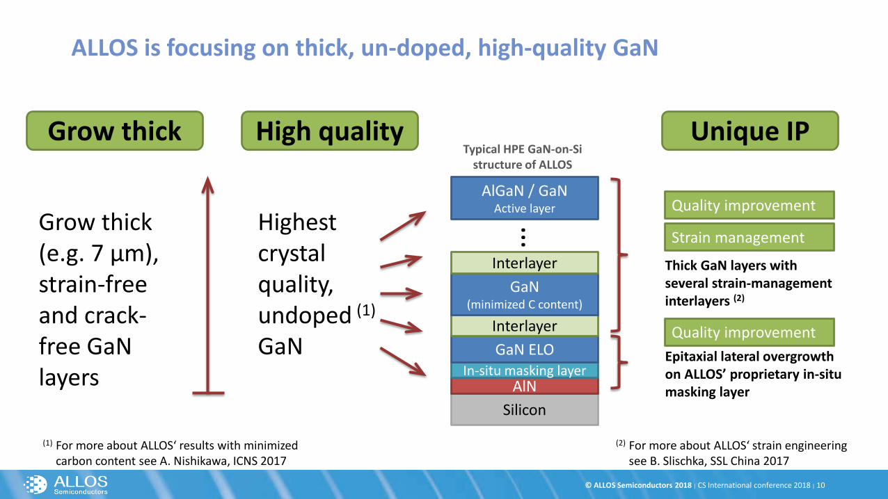
ALLOS is focusing on thick, un-doped, high-quality GaN
SiliconAlN
In-situ masking layerGaN ELOInterlayer
GaN(minimized C content)
Interlayer
AlGaN / GaNActive layer…
Epitaxial lateral overgrowth on ALLOS’ proprietary in-situ masking layer
Thick GaN layers with several strain-management interlayers (2)
Quality improvement
Quality improvement
Strain management
Typical HPE GaN-on-Sistructure of ALLOS
Grow thick(e.g. 7 µm), strain-freeand crack-free GaNlayers
Grow thick High quality Unique IP
Highestcrystalquality, undoped (1)
GaN
(1) For more about ALLOS‘ results with minimizedcarbon content see A. Nishikawa, ICNS 2017
(2) For more about ALLOS‘ strain engineeringsee B. Slischka, SSL China 2017

© ALLOS Semiconductors 2018 | CS International conference 2018 | 11
0 200 400 600 800 1000 1200 1400 160010-12
10-11
10-10
10-9
10-8
10-7
10-6
10-5
10-4
10-3
10-2
Cur
rent
(A)
Voltage (V)
600 V product 1200 V product
This thick, high quality and optimized GaN stack results in an Ec of 2 MV/cm and a vertical Vbr of over 1400 V for 7 µm thick GaN
Vertical breakdown(600 V and 1200 V products)
Ec of~2.0 MV/cm
Data by courtesy of Dr. Farid Medjdoub and team at IEMN
2DEG channel disabled

© ALLOS Semiconductors 2018 | CS International conference 2018 | 12
The critical electric field is as high as 1.7 MV/cm for lateral, floating breakdown measurements
0 10 20 30 40 50 60 70 80 90 1000
500
1000
1500
2000
2500
1200 V product
Brea
kdow
n vo
ltage
(V)
Contact distance (µm)
12 µm
Lateral floating breakdown as a function of electrode spacing (1200 V product)
Data by courtesy of Dr. Farid Medjdoub and team at IEMN
0 500 1000 1500 200010-10
10-9
10-8
10-7
10-6
10-5
10-4
10-3
Cur
rent
(A)
Voltage (V)
4 um 8 um 12 um 24 um 48 um 64 um 96 um
Lateral floating breakdown with different electrode spacing (1200 V product)
4 µm 8 µm 12 µm
Ec of~1.7 MV/cm
2DEG channel disabled
© ALLOS Semiconductors 2018 | CS International conference 2018 | 13
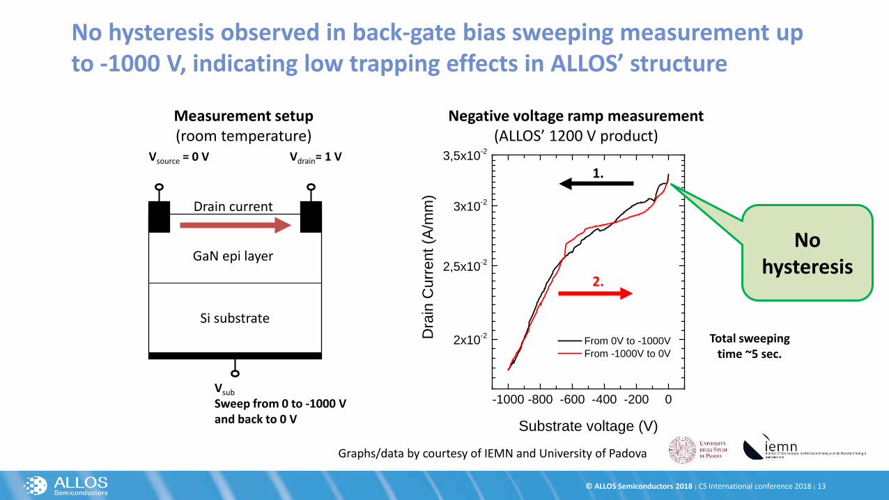
No hysteresis observed in back-gate bias sweeping measurement up to -1000 V, indicating low trapping effects in ALLOS’ structure
-1000 -800 -600 -400 -200 0
2x10⁻²
2,5x10⁻²
3x10⁻²
3,5x10⁻²
Dra
in C
urre
nt (A
/mm
)Substrate voltage (V)
From 0V to -1000V From -1000V to 0V
Vsource = 0 V Vdrain= 1 V
VsubSweep from 0 to -1000 Vand back to 0 V
Measurement setup(room temperature)
Negative voltage ramp measurement(ALLOS’ 1200 V product)
GaN epi layer
Si substrate
Graphs/data by courtesy of IEMN and University of Padova
Drain current
1.
2.
No hysteresis
Total sweeping time ~5 sec.

© ALLOS Semiconductors 2018 | CS International conference 2018 | 14
Back-gating transient measurements show very low trapping effects in ALLOS’ GaN doping-free buffer with negative bias up to -800 V
Graphs/data by courtesy of IEMN and University of Padova
Drain current measured during negative bias up to -800 V
Back-gating transient measurement(1200 V product, room temperature)
Back-gating transient measurement setup
10-4 10-3 10-2 10-1 100 101 102 1030,012
0,013
0,014
0,015
0,016
Dra
in c
urre
nt (A
)Negative bias time (sec)
-200V -300V -400V -500V -600V -700V -800V
Substrate voltage:
820 µs100 s Only very
small current drop

© ALLOS Semiconductors 2018 | CS International conference 2018 | 15
This product prototype for 1200 V is based on ALLOS’ established 600 V product and its superior quality and performance
Lowest possible residual strain 200 mm (725 µm thick) and 150 mm (625 µm) 7 µm thick with 0.3 % uniformity 30 µm bow, no cracks, thinning possible
Highest crystal quality XRD: 315 arcsec for (002), 415 arcsec for (102) TDD: 2x108 cm-2
Very low leakage currents and high breakdown voltage 0.003 µA/mm² vertical, 0.005 µA/mm lateral @ 600 V
Excellent Hall data Rsheet: 340 Ω/sq., Mobility ~2000 cm²/Vs
ALLOS 200 mm GaN-on-Si epiwafer (600 V product)

© ALLOS Semiconductors 2018 | CS International conference 2018 | 16
A. Why is GaN-on-Si limited to 600 V today?
B. What can be achieved with ALLOS’ technology?
C. Vision: How to attack SiC with 1200 Volt GaN-on-Si devices?

© ALLOS Semiconductors 2018 | CS International conference 2018 | 17
0
0.05
0.1
0.15
0.2
0.25
0.3
0 5 10 15 20 25 30 35 40
Rds o
n (o
hm)
Current (A)
Rdson vs Current
GaN can show its advantage in Rdson already today
900 V
650 V, 22.5 A650 V
650 V
650 V
900 V, 36 A
900 V, 23 A
1200 V, 36 A
Commercial SiCdevice vendorCommercial GaN-on-Sidevice vendor
Let‘s have a look at this area
* Rmaterial stands here for the resistance properties of the respective materials used. In GaN in particular sheet resistance Rsheet
In vertical devices „contact distance“ is also commonly known as „drift region“
𝑅𝑅𝑑𝑑𝑑𝑑𝑑𝑑𝑑𝑑 =𝑓𝑓 𝑅𝑅𝑚𝑚𝑚𝑚𝑚𝑚𝑚𝑚𝑚𝑚𝑚𝑚𝑚𝑚𝑚𝑚; 𝑐𝑐𝑑𝑑𝑑𝑑𝑚𝑚𝑚𝑚𝑐𝑐𝑚𝑚 𝑑𝑑𝑚𝑚𝑑𝑑𝑚𝑚𝑚𝑚𝑑𝑑𝑐𝑐𝑚𝑚; 𝑅𝑅𝑐𝑐𝑑𝑑𝑑𝑑𝑚𝑚𝑚𝑚𝑐𝑐𝑚𝑚 *

© ALLOS Semiconductors 2018 | CS International conference 2018 | 18
0
0.05
0.1
0.15
0.2
0.25
0.3
0 5 10 15 20 25 30 35 40
Rds o
n (o
hm)
Current (A)
Rdson vs Current
23 %
Going to 1200 V increases Rdson for SiC by 23 %
900 V
650 V, 22.5 A650 V
650 V
650 V
900 V, 23 A, 0.12 Ohm
23 %
1200 V, 23 A, 0.15 Ohm
SiC 1200 V, 23 A, based on increase at 36 A
Estimate / projection:
Commercial SiCdevice vendorCommercial GaN-on-Sidevice vendor
900 V, 36 A
1200 V, 36 A
𝑅𝑅𝑑𝑑𝑑𝑑𝑑𝑑𝑑𝑑 = 𝑓𝑓 𝑅𝑅𝑚𝑚𝑚𝑚𝑚𝑚𝑚𝑚𝑚𝑚𝑚𝑚𝑚𝑚𝑚𝑚; 𝑐𝑐𝑑𝑑𝑑𝑑𝑚𝑚𝑚𝑚𝑐𝑐𝑚𝑚 𝑑𝑑𝑚𝑚𝑑𝑑𝑚𝑚𝑚𝑚𝑑𝑑𝑐𝑐𝑚𝑚; 𝑅𝑅𝑐𝑐𝑑𝑑𝑑𝑑𝑚𝑚𝑚𝑚𝑐𝑐𝑚𝑚
Needs to increase to sustain 1200 V23 % increase

© ALLOS Semiconductors 2018 | CS International conference 2018 | 19
0
0.05
0.1
0.15
0.2
0.25
0.3
0 5 10 15 20 25 30 35 40
Rds o
n (o
hm)
Current (A)
Rdson vs Current
Moving to 1200 V with GaN does not increase Rdson
900 V
650 V and 1200 V, 22.5 A650 V and 1200 V
650 V and 1200 V
650 V and 1200 V
900 V, 36 A
900 V, 23 A, 0.12 Ohm
1200 V, 40 A
1200 V, 23 A, 0.15 Ohm
𝑅𝑅𝑑𝑑𝑑𝑑𝑑𝑑𝑑𝑑 = 𝑓𝑓 𝑅𝑅𝑚𝑚𝑚𝑚𝑚𝑚𝑚𝑚𝑚𝑚𝑚𝑚𝑚𝑚𝑚𝑚; 𝑐𝑐𝑑𝑑𝑑𝑑𝑚𝑚𝑚𝑚𝑐𝑐𝑚𝑚 𝑑𝑑𝑚𝑚𝑑𝑑𝑚𝑚𝑚𝑚𝑑𝑑𝑐𝑐𝑚𝑚; 𝑅𝑅𝑐𝑐𝑑𝑑𝑑𝑑𝑚𝑚𝑚𝑚𝑐𝑐𝑚𝑚
Same distance with ALLOS’ GaN-on-SiSame Rdson!
SiC at 1200 VEstimate / projection:
Commercial SiCdevice vendorCommercial GaN-on-Sidevice vendor
ALLOS GaN-on-Siat 1200 V

© ALLOS Semiconductors 2018 | CS International conference 2018 | 20
0
0.05
0.1
0.15
0.2
0.25
0.3
0 5 10 15 20 25 30 35 40
Rds o
n (o
hm)
Current (A)
Rdson vs Current
At 1200 V the SiC Rdson value is twice the GaN-on-Si Rdson value
900 V
650 V and 1200 V, 22.5 A650 V and 1200 V
650 V and 1200 V
650 V and 1200 V
900 V, 36 A
900 V, 23 A, 0.12 Ohm
1200 V, 40 A
SiC at 1200 V
1200 V, 23 A, 0.15 Ohm
Estimate / projection:
Commercial SiCdevice vendorCommercial GaN-on-Sidevice vendor
ALLOS GaN-on-Siat 1200 V
> 2 x Rdson

© ALLOS Semiconductors 2018 | CS International conference 2018 | 21
The cost comparison shows a strong starting position for SiC
SiC offers 15 % lower costfor a higher voltage!
Commercial SiCdevice vendorCommercial GaN-on-Sidevice vendor
(1) Estimate based on cost increase from 900 V to 1200 V for 36 A devices
GaN-on-Si device 650 V,
22.5 A, 150 mm
SiC device 900 V, 23 A,
100 mm
SiC device 1200 V, 23 A,
100 mm (1)

© ALLOS Semiconductors 2018 | CS International conference 2018 | 22
At 1200 V GaN-on-Si gets a cost advantage
10 % increase in cost whengrowing 7 µm thick GaN
11 %
Commercial SiCdevice vendorCommercial GaN-on-Sidevice vendor
When using ALLOS’ GaN-on-Si
Estimate / projection:
GaN-on-Si device 650 V,
22.5 A, 150 mm
SiC device 900 V, 23 A,
100 mm
SiC device 1200 V, 23 A,
100 mm
GaN-on-Sidevice 1200 V,
22.5 A, 150 mm

© ALLOS Semiconductors 2018 | CS International conference 2018 | 23
ALLOS’ GaN-on-Si can scale to 200 mm saving at least 35 % cost
35 % cost reductionwhen moving to 200 mm
Commercial SiCdevice vendorCommercial GaN-on-Sidevice vendor
When using ALLOS’ GaN-on-Si
Estimate / projection:
GaN-on-Si device 650 V,
22.5 A, 150 mm
SiC device 900 V, 23 A,
100 mm
SiC device 1200 V, 23 A,
100 mm
GaN-on-Sidevice 1200 V,
22.5 A, 150 mm
GaN-on-Sidevice 1200 V,
22.5 A, 200 mm

© ALLOS Semiconductors 2018 | CS International conference 2018 | 24
SiC needs to solve its yield issues at 150 mm to reduce cost
Commercial SiCdevice vendorCommercial GaN-on-Sidevice vendor
When using ALLOS’ GaN-on-Si
Estimate / projection:
Migration to 150 mm SiCif yield is sufficient
GaN-on-Si device 650 V,
22.5 A, 150 mm
SiC device 900 V, 23 A,
100 mm
SiC device 1200 V, 23 A,
100 mm
GaN-on-Sidevice 1200 V,
22.5 A, 150 mm
GaN-on-Sidevice 1200 V,
22.5 A, 200 mm
SiC device 1200 V, 36 A,
150 mm

© ALLOS Semiconductors 2018 | CS International conference 2018 | 25
At 1200 V ALLOS’ technology on 200 mm enables a cost advantage
GaN-on-Si device 650 V,
22.5 A, 150 mm
SiC device 900 V, 23 A,
100 mm
SiC device 1200 V, 23 A,
100 mm
Commercial SiCdevice vendorCommercial GaN-on-Sidevice vendor
When using ALLOS’ GaN-on-Si
GaN-on-Sidevice 1200 V,
22.5 A, 150 mm
GaN-on-Sidevice 1200 V,
22.5 A, 200 mm
Estimate / projection:
16 %
42 %
SiC device 1200 V, 36 A,
150 mm

© ALLOS Semiconductors 2018 | CS International conference 2018 | 26
Summary: 1200 V GaN-on-Si can attack SiC on performance and price
650 V150 mm
1200 V150 mm
1200 V200 mm
1200 V100 mm
900 V100 mm
SJ MOSFET
Commercial SiCdeviceCommercial GaN-on-Sidevice
Estimate / projection:
When using ALLOS’ GaN-on-Si
SJ MOSFET benchmark
1200 V150 mm
SiC at 1200 V
Less than half the Rdson of SiC
16 % lower cost
© ALLOS Semiconductors 2018 | CS International conference 2018 | 27
Conclusion and outlook
ALLOS’ GaN-on-Si is the right basis to advance into SiC territory1. A Vbr of 1400 V vertical and lateral is achieved2. Indications for very low trapping effects3. The existing Rdson advantage of GaN-on-Si over SiC is expected to widen
further when moving to 1200 V devices4. 200 mm wafer for 1200 V provide a cost advantage over SiC 100 and 150 mm
ALLOS seeks a partner to develop and commercialize this technology• Accelerating existing epi development program• Working for device vendors to combine the strengths of this material and
advanced device technology• Identify and target attractive applications above 650 V

Visit ushttp://www.allos-semiconductors.com
Follow ushttps://www.linkedin.com/company/allos-semiconductors-gmbhhttps://twitter.com/ALLOSsemi
Thank you for voting for us!
ALLOS Semiconductors GmbHBurkhard Slischka, CEOBreitscheidstrasse 78, 01237 Dresden, Germany
[email protected] Office: +49-351-212 937-0Fax: +49-351-212 937-99
Thank you for nominating us!


![[NE Handbook series ] Power Devices - Symmetron · 6 Power Devices 9 Power MOSFET ... 17 SiC wafer 19 GaN wafer 21 SiC and GaN 22 Chapter 2: R&D of Next-generation Power ... and miniaturization](https://static.fdocuments.in/doc/165x107/5ae834877f8b9a08778f6709/ne-handbook-series-power-devices-power-devices-9-power-mosfet-17-sic-wafer.jpg)