High Power Semiconductor Diode Lasers - …cdn.intechweb.org/pdfs/20488.pdf · 16 Recent...
25
16 Recent Developments in High Power Semiconductor Diode Lasers Li Zhong and Xiaoyu Ma National Engineering Research Center for Optoelectronic Devices, Institute of Semiconductors, Chinese Academy of Sciences Beijing China 1. Introduction Due to a number of advantages of diode lasers, such as small size, light weight, high efficiency etc., it has been the focus of the laser field from the beginning of the birth and has been widely used in industrial, military, medical, communications and other fields. Especially, to a great extent, a tremendous growth in the technology of solid-state lasers has been complemented by laser diode array designs for pumping such solid-state lasers. Significant applications continue to exist at common solid state laser systems such as yttrium aluminum garnet doped with neodymium or ytterbium (Nd:YAG or Yb:YAG, respectively) requiring pump light in the 780 nm to 1000 nm range. Driven by the increasing demands of high-performance high-power laser pumping source and direct industrial processing applications, tremendous breakthrough have been realized in the main optical- electronic performances of high power semiconductor diode lasers, such as ultra-high peak power, super-high electro-optical conversion efficiency, low beam divergence, high brightness, narrow spectrum linewidth, high operation temperature, high reliability, wavelength stabilization and fundamental transverse mode operation etc. These achievements are attributed to a combination of the maturity of semiconductor material epitaxy, the optimization of the laser waveguide structure, the cavity surface-passivation technology as well as the high effective cooling and packaging technologies. The Occident and Japan keep ahead in this field with several large corporations actively engaged in this market, for example, Coherent, IMC, SDL, OPC, HPD, Spectrum-Physics of the U.S., OSRAM, JOLD, Frauhorf of Germany, THALES of France, SANYO, SONY of Japan, and ATC of Russia etc. The wavelength of these industrial products ranges from 630 nm to 1550 nm, and optical output power levels from several W to 10 kW class. In China, prominent progresses have also been made at a rapid rate. Advances in the design and manufacture of the bars, together with effective means of stacking and imaging monolithic semiconductor laser arrays (bars), have enabled the production of robust sources at market- competitive costs. In particular, the diode lasers for these systems have to meet high demands in relation to efficiency, power, reliability and manufacturability, which following the desire for reducing the cost per watt and the cost per hour’s lifetime for the customer. However, with the enhancement of the power and beam quality, a series of new practical problems arise in the aspect of engineering, such as high cost of the high-current and low- www.intechopen.com
Transcript of High Power Semiconductor Diode Lasers - …cdn.intechweb.org/pdfs/20488.pdf · 16 Recent...
16
Recent Developments in High Power Semiconductor Diode Lasers
Li Zhong and Xiaoyu Ma National Engineering Research Center for Optoelectronic Devices,
Institute of Semiconductors, Chinese Academy of Sciences Beijing China
1. Introduction
Due to a number of advantages of diode lasers, such as small size, light weight, high efficiency etc., it has been the focus of the laser field from the beginning of the birth and has been widely used in industrial, military, medical, communications and other fields. Especially, to a great extent, a tremendous growth in the technology of solid-state lasers has been complemented by laser diode array designs for pumping such solid-state lasers. Significant applications continue to exist at common solid state laser systems such as yttrium aluminum garnet doped with neodymium or ytterbium (Nd:YAG or Yb:YAG, respectively) requiring pump light in the 780 nm to 1000 nm range. Driven by the increasing demands of high-performance high-power laser pumping source and direct industrial processing applications, tremendous breakthrough have been realized in the main optical-electronic performances of high power semiconductor diode lasers, such as ultra-high peak power, super-high electro-optical conversion efficiency, low beam divergence, high brightness, narrow spectrum linewidth, high operation temperature, high reliability, wavelength stabilization and fundamental transverse mode operation etc. These achievements are attributed to a combination of the maturity of semiconductor material epitaxy, the optimization of the laser waveguide structure, the cavity surface-passivation technology as well as the high effective cooling and packaging technologies. The Occident and Japan keep ahead in this field with several large corporations actively engaged in this market, for example, Coherent, IMC, SDL, OPC, HPD, Spectrum-Physics of the U.S., OSRAM, JOLD, Frauhorf of Germany, THALES of France, SANYO, SONY of Japan, and ATC of Russia etc. The wavelength of these industrial products ranges from 630 nm to 1550 nm, and optical output power levels from several W to 10 kW class. In China, prominent progresses have also been made at a rapid rate. Advances in the design and manufacture of the bars, together with effective means of stacking and imaging monolithic semiconductor laser arrays (bars), have enabled the production of robust sources at market-competitive costs. In particular, the diode lasers for these systems have to meet high demands in relation to efficiency, power, reliability and manufacturability, which following the desire for reducing the cost per watt and the cost per hour’s lifetime for the customer. However, with the enhancement of the power and beam quality, a series of new practical problems arise in the aspect of engineering, such as high cost of the high-current and low-
www.intechopen.com

Optoelectronics – Devices and Applications
326
voltage power supply and short life span of micro-channel heat sink cooling etc.. Gradually, single-emitter semiconductor laser devices and mini-bars with high power and high beam quality are becoming the mainstream research trend and replacing the traditional cm-bars. On the other hand, the reduced divergence angle accelerates the improvement of beam quality, which is directly reflected in the decrease of the fiber diameter and the increase of the output power for fiber-coupled diode laser module. Here we review and discuss the state of the art of high power semiconductor diode lasers, including single emitters, bars, horizontal bar arrays and vertical bar stacks, with the typical data presented. Several key technological problems concerning the improvements of diode lasers performance, the optimization of packaging architectures and the developments of high beam quality of diode lasers will be discussed in section 2~5, respectively. In section 6, we conclude with some thoughts on the future study directions and the developing tendency for high power diode lasers.
2. Status of high-power diode laser technology and characteristics
2.1 Laser diode chip technology Over the recent years, high power diode lasers have seen a tremendous evolution in material epitaxial growth technology, epi-structure optimization technique, cavity surface-passivation technology etc.. Epitaxial structure is designed for a specific range of operation to optimize a combination of optical, electrical and thermal performance, generally minimizing both operating voltage and internal loss to achieve high efficiency with long cavities for high-average-power and high-brightness applications. The details of these structures, such as material compositions, layer thicknesses, asymmetric or symmetric waveguide structure design, and doping profiles are selected to ensure that manufacturability and reliability are not compromised. Important developments in epitaxial growth technology include the reporting of low loss materials (about 1 cm–1 for AlGaAs for example), the development of the strained materials with attendant benefits on gain and bulk defect pinning, and the development of aluminum-free materials such as InGaAs and InGaAsP with the latter material having been reported to wavelengths below 800 nm. A number of careful studies are being reported on filament formation and current crowding in semiconductor lasers and methods for avoiding their deleterious effects. With the improvement of the high-quality, low defect density epitaxial growth technology of semiconductor materials, the resonator cavity length of the existing cm bar has been increased from 0.6 ~ 1.0 mm to 2.0 ~ 5.0 mm, making a significant increase of the output power. The large cavity length ensured low thermal and electrical resistivities of the devices by increasing their active area. The cavity length is selected mainly depending on desired operation power and is optimized for best power conversion efficiency (PCE) at the given condition. In continuous wave (CW) operation the output power from high power laser bars usually is limited by the thermal load that the assembly may dissipate. Failure modes, like wear out of the output power or bulk failures are critical in CW operation. For quasi continuous wave (qCW) applications the reliable output power in general is not thermally limited. The robustness of the output facet of the devices and the degradation of the assembly under the cyclic thermal load become the critical matter. Special methods of facet design and treatment have been employed to increase the COMD power threshold and suppress its degradation over the operating life of the device, such as facet passivation with a dielectric layer,
www.intechopen.com

Recent Developments in High Power Semiconductor Diode Lasers
327
regrown non-absorbing mirror (ReNAM), intermixed non-absorbing mirror (iNAM), ultra-high vacuum (UHV) cleaved facets etc..(Yanson et al., 2011) NAM-based techniques (ReNAM and iNAM) require further development to achieve required reliability figures. Dielectric passivation and cleave-in-a-vacuum techniques are found to be the two best performing facet engineering solutions. At 980nm, dielectric facet passivation can be employed with a pre-clean cycle to deliver a device lifetime in excess of 3,000 hours at increasing current steps. Vacuum cleaved emitters have delivered excellent reliability at 915nm, and can be expected to perform just as well at 925 and 980nm. By preventing exposure of a freshly cleaved facet to oxygen, the formation of surface oxides and shallow levels is avoided without the need for ion plasma cleaning.(Tu et al., 1996) A capping layer, also deposited in a vacuum, seals the facet and stops the penetration of oxygen. Single emitters fabricated with these two techniques are packaged into fiber-coupled modules with 10W output and 47% efficiency. (Tu et al., 1996)
2.2 Far field divergence angle control As the basic unit of the integration of semiconductor laser system, the performance of different structure and different types of semiconductor laser device directly contributes to the development of semiconductor laser systems, one of the most important developments is the reduction of the beam divergence and the increase of the output power. According to the definition of the beam quality, the beam divergence angle is proportional to the beam-parameter product (Q or BPP), which is a measure of the beam quality. Therefore the beam quality is under the direct control of the far field divergence angle. Overall, the waveguide structure of semiconductor lasers leads to a serious asymmetry far-field beam quality. In the fast axis direction, the output beam can be considered to be fundamental mode, but the divergence angle is large. The compression of the fast axis divergence angle can effectively reduce the requirements for the fast axis collimator aperture. While in the slow axis direction, the output beam is multi-mode and the beam quality is poor. The beam quality can be directly improved by reducing the divergence angle in the slow axis direction, which is the research focus in the field of the high-beam quality semiconductor laser. The research focus in the control of the fast axis divergence angle is how to balance the fast axis divergence angle and the electro-optical conversion efficiency. Although a number of research institutions had press release of the continued access to fast axis divergence angle of only 3° and even 1°, but based on the consideration of the power, the electro-optical conversion efficiency and the cost, it is difficult to promote practical applications in the short term. In the early year of 2010, the P. Crump etc. of German Ferdinand-Braun Institute has reported the fast axis divergence angle of 30° (95% of the energy range) obtained through the use of large optical cavity and low-limiting factors, meanwhile the electro-optical conversion efficiency of the device is 55%, which is the basic standards to practical devices. The fast axis divergence angle of the current commercial high-power semiconductor laser devices are also dropped from the original of about 80° (95% of the energy range) to below 50°, which substantially lower the requirements for the numerical aperture of the collimator. In the slow-axis divergence angle control, recent studies have shown that, in addition to the device's own structure, the combination of the drive current density and the thermal effects of semiconductor lasers affect the slow axis divergence angle. The slow axis divergence of a single emitter with long cavity length is of the most easy to control,
www.intechopen.com

Optoelectronics – Devices and Applications
328
whereas in the array device, with the increase of the fill factor, the intensification of thermal cross-talk between the emitting elements will lead to the increase of the slow-axis divergence angle. In the year of 2009, the Bookham company of Switzerland has successfully reduced the slow-axis divergence (95% of the energy range) of 9xx-nm 10 W commercial devices with 5 mm cavity length from 10o ~ 12o to about 7o. In the same year, the Osram Company of German and the Coherent Company of the United States has reduced the slow-axis divergence of the array (95% of the energy range) to 7o level.
2.3 High-temperature performance of laser bars and arrays Since the performance of a diode laser is operating temperature dependent, high-power
diode laser pump modules usually need a cooling system to control their operating
temperature. However, some diode laser applications require that high-power diode laser
pump modules operate in a high temperature environment without any cooling. In
addition, the diode laser pump modules have to provide both high peak power and a nice
pulse shape because certain energy in each pulse is required. At such a high temperature,
semiconductor quantum well gain drops significantly, and the carrier leakage and the
Auger recombination rate increases. Thus, the laser bar has a high threshold and low
slope efficiency, resulting in very low power efficiency. To reach certain power level at
high temperature, the pump current has to be much higher than that at room temperature.
More waste heat is generated in the active region of the diode laser bar. In addition, tens
of milliseconds pulse width with a few percent duty cycle forces the laser bar to operate in
a “CW” mode.(Ziegler et al., 2006; Puchert et al., 2000; Voss et al., 1996) The Lasertel
Company has presented the development of high-temperature 8xx-nm diode laser bars
for diode laser long-pulse (>10 milliseconds) pumping within a high-temperature (130 ºC)
environment without any cooling.( Fan et al., 2011) The epi-structure is based on a large
optical cavity separate confinement heterostructure with Al-free active region. By
adjusting Aluminum concentration in the AlGaInP barrier, introducing strain in quantum
well (QW) and adjusting the width of QW, optimizing the strain and the width of
quantum well, the gain is maximized, the loss and carrier leakage especially at high
temperature is minimized and the optical confinement of the waveguide is also be
improved. Under the operation condition (130 ºC, 15 ms pulse width, 5 Hz frequency and
100-A current pulse), the high-temperature laser bars show robust and consistent
performance, reaching 60 W (peak) power and having good pulse shape, as shown in
Figure 1. The laser bars do not show any degradation after 310,000 15-millisecond current
pulse shots. They demonstrated over 40-millisecond long-pulse operation of the 8xx-nm
CS bars at 130 ºC and 100 A. Regardless of the pulse shape, this laser bar can lase at
extremely high temperature and output pulse can last for 8 ms/2ms at 170 ºC/180 ºC
respectively, both driven by 60 A current pulses with 5-Hz frequency, 10 millisecond
pulse width. This is the highest operating temperature for a long-pulse 8xx-nm laser bar.
Figure 2 shows the high-temperature performance of the 3-bar stack array and its pulse
shape at 130 ºC. The peak power of the 3-bar array reaches 165 kW at 100A and 130 ºC, but
the pulse shape is very sensitive to the current and the power of the array drops much
faster than that of the CS bar, which may be attributed to the package difference between
the CS bar and stack array.
www.intechopen.com

Recent Developments in High Power Semiconductor Diode Lasers
329
Fig. 1. Pulsed (15 msec PW and 5 Hz frequency) L-I performance and wall-plug efficiency at 130°C.
Fig. 2. High temperature performance of 3-bar array (left) and its pulse shape at 130 ºC (right).
3. The latest high-power semiconductor laser devices
3.1 Developments of the standard cm laser diode bar The increasing of reliable power level of diode lasers will enable wider deployment, higher power systems and new market which were previously unavailable, such as direct materials processing etc. Also, it will lead to lower cost to the user, per watt of useable output. The standard length of the laser bars of 1 cm array has been established to obtain high power output, i.e. many emitters has been lateral parallel monolithic integrated in the scale of the slow axis direction into one diode laser bar, Laser bars provide a magnitude of output power of single emitter by integration the single emitters at the wafer level, which has long been a most commonly used form for high-power semiconductor lasers. According to the application, whether high brightness or high power operation is intended, the filling factor is varied between 10% to 80%. In the early year of 2008, the Spectra-Physics Company of the United States reported the access of 800 W/bar, 1010 W/bar, 950 W/bar maximum output power respectively from the center wavelength of 808 nm, 940 nm, 980 nm cm bar, with corresponding maximum PCE
www.intechopen.com

Optoelectronics – Devices and Applications
330
values of 54.3%, 67.4%, and 70%. (Li et al., 2008) Figure 3 summarizes the P-I-PCE curves of bars.
Fig. 3. P-I-PCE curves of bars with double-side cooling from the Spectra-Physics Lasers Company.
All of the bars had a FF of 83% (65 emitters, each 125-μm wide and 5.0-mm long, with a
separation of 150 μm). All bars were bonded using the double-sided micro-channel heat sink
cooling technology with the circulating water at 5-8°C (Li et al., 2008). These output power
are the maximum continuous output power level of the current laboratory. In addition,
many other semiconductor laser company, such as the German company JENOPTIK,
Switzerland company Oclaro also continued to prepare the kilowatt diode laser array. J.
Müller ect. of the Oclaro has made it clear that the access to 1.5 kW/bar array devices is not
a problem based on the existing technologies. At the same time, the output power of high
beam quality, low fill factor cm bar is also increasing. Table 1 gives the BPP value of cm bars
with different fill factors obtained by the Limo Company of German. From the results of
Table 1, it can be concluded that for a certain horizontal dimensions of semiconductor laser
array device, in the case of the same divergence angle, the BPP value is proportional to the
fill factor, i.e. the lower the fill factor, the smaller of the BPP value, and the better the beam
quality. Currently, In the 9xx-nm wavelength range 150 W or higher CW output power
levels have become the standard for high filling factor bars.( Lichtenstein et al., 2005; Krejci
et al., 2009; Crump et al., 2006) In the 80x range devices with 100 W and more output power
were demonstrated (Tu et al., 1996; Ziegler et al., 2006). The output characteristic of an 808
nm device optimized for 140-160 W CW output power is shown in Figure 4 (Müller et al.,
2010).An output power of 185 W is achieved for CW 200A drive current. For currents above
180 A the thermal limitation of the device is clearly visible in a pronounced rolling of the P-I
curve limiting the achievable brightness in this operation mode. The output power of 9xx-
nm cm bar with 20% fill factor is up to 180 W/bar in CW condition, the BPP value is down
to 5.9 mm·mrad after the symmetry of the fast and slow axis of the beam, and the
commercial devices can be work above the level of 80 W/bar with long-term stability; the
www.intechopen.com

Recent Developments in High Power Semiconductor Diode Lasers
331
Emitter Width (μm) 100 200 150 100 5 Pitch (μm) 200 400 500 500 200
Number of Emitters 49 24 19 19 49 Filling Factor (%) 50 50 30 20 2.5
Beam Divergence FA (FW 90%) (°)
80 80 80 80 80
Beam Divergence SA (FW 90%) (°)
12 12 12 12 12
BPP FA (mm·mrad)
0.35 0.35 0.35 0.35 0.35
BPP SA (mm·mrad)
257 251 149 100 13
Ratio BPP SA/BPP FA
735 720 428 285 37
Symmetrized BPP (mm·mrad)
9.5 9.4 7.2 5.9 2.1
Beam Diameter at NA=0.22 (μm)
121 120 92 75 27
Table 1. the BPP of cm bars with different structures.
output power of 2.5 % fill factor cm bar is up to 50 W/bar in CW condition, the BPP value is down to 2.1 mm·mrad after the symmetry of the fast and slow axis of the beam, the current device is still under developing, and need to improve the stability further. The reliable output power of CW operated bars is in first place limited by the cooling capability of the assembly. Bars operated in a qCW mode deliver a significantly higher reliable output power, because the thermal load is reduced by a factor which is inverse proportional to the duty cycle of the operation mode. Figure 5 and 6 give the typical performance of our lab’s 808nm laser diode bar packaged by conductive heatsink (qCW 300 W/barand 200 W/bar with 60% PCE) and 980nm laser diode bar packaged by micro-channel heatsink (CW 200W/bar), respectively.
Fig. 4. PIV-PCE characteristic of a 50% filling factor 808 nm bar on micro channel cooler at 25 °C water temperature from the Oclaro Company.
www.intechopen.com

Optoelectronics – Devices and Applications
332
Fig. 5. The typical P-I-V curve and spectrum of 808-nm bar packaged by conductive heatsink in our lab. (a) qCW 300 W/barand (b) qCW 200 W/bar with 60% PCE
Fig. 6. The typical P-I curve of CW 200 W/bar 980-nm bar packaged by microchannel heatsink in our lab.
However, with the requirement for the decrease of the fill factor to increase the output power and increase the beam quality, a series of new problems arise gradually, especially high cost problem of its accompanying high-current and low-voltage power supply and short life span problem of the micro-channel heat sink cooling etc. Most of the power test of cm bar is subject to the limit of maximum current supply, instead of its own output power limit. In engineering, a combination of several volts with several hundreds of current will produce many practical problems. On the other hand, the micro-channel heat sink must be used to dissipate the high heat flux generated by the cm bar with ultra-high power and high beam quality, but the utmost ability of heat dissipation for the existing water-cooled micro-channel heat sink is no doubt become the biggest obstacle for the further improvements of power and beam quality. The recent developed double-sided micro-channel cooling technology has limited effect on reducing the thermal resistance, and it doesn’t seem to satisfy the sustainable expansibility for the power enhancement of the cm bar. In addition, it also can not be ignored that the relatively short life span of the micro-channel heat sink has been the current bottleneck for high-power semiconductor lasers. Although there are some other new efficient technologies arise, such as phase change thermal cooling, spray cooling
www.intechopen.com

Recent Developments in High Power Semiconductor Diode Lasers
333
and micro-heat-pipe technology etc., it is difficult to satisfy the practical applications in the short term because of the performance characteristics, the cost and the compatibility problems. Due to the two constraints mentioned above, in recent years, the major research institutions and high-power semiconductor laser suppliers no longer blindly pursue the improvement of the output power of cm bars, but gradually shift the focus to develop single emitter and mini bars with high power and good beam quality.
3.2 Developments of the single emitter Compared with the cm bar, the single emitter, which possesses the independent electrical and thermal operation environment, can avoid the thermal crosstalk between the emitting units, so that to have the obvious advantages in life span and beam quality. In addition, owing to the low drive current of the single emitter, the requirement for the drive power can be reduced significantly even in the serial operation. Meanwhile, the heat from a single emitter is relatively low, so the conduction heat sink can be used directly for heat dissipation to avoid the short life span problem brought by the micro-channel heat sink. And the independent thermal operation environment can make it operate under high power density. Currently, optical power linear density of a single emitter can be up to above 200 mW/μm with narrow spectral width, while that of a cm bar is only about 50~85 mW/μm. Especially, the independent thermal and electrical operation environment can make a significant reduction in the risk of device failure. Under the support of the high stable gold tin solder packaging technology, average life of the commercial high-power single emitters can reach to above 100 thousands hours, which is much higher than that of cm bars and hence reduces the use-cost of devices. Based on the advantages listed above, the single emitter exhibits the trend that it will replace the cm bar gradually to become the mainstream semiconductor laser device with high power and high beam quality. In recent years, single emitters have been developed rapidly. Especially driven by the
demand of high power fiber lasers for high-brightness fiber-coupled pumping modules, the
single emitters with 90~100 μm strip width, which is matched to the 105 μm/125 μm
multimode fiber tail, are improved significantly in output power and beam quality.
Currently, the continuous output power of 9xx-nm single emitters can reach 20~25
W/emitter; while that for 8xx-nm can be also beyond 12 W/emitter. In terms of the
commercial devices, the 9xx-nm single emitters with the stripe width of 90~100 μm,
prepared by IPG, Oclaro, JDSU and other high-power semiconductor laser device suppliers,
can operate continuously and steadily over 10 W/emitter, and above 100 W output power
can be achieved from the synthesis of the fiber-coupled multiple single emitters.
3.3 Developments of the mini-bar devices Although the output power of the single emitter is improved rapidly, there is still a wide
gap compared to the cm bar. To meet the needs of different applications on power, mini-bar,
a new type of high-power semiconductor laser devices, appears and is being developed
rapidly. The mini-bar is obtained by integrating several single emitters on a substrate, which
is actually the compromise and optimization in the structure of the cm bar and the single
emitter. It combines the advantages of the cm bar and the single emitter, and its drive
current, lifetime, output power density and spectral width are between those of the cm bar
and the single emitter. Also taking into account the high beam quality and the demand for
fiber laser pumping source, the development of the mini-bar mainly focuses on the low fill
www.intechopen.com

Optoelectronics – Devices and Applications
334
factor devices with the strip width of 100 μm. In 2009, the Osram Company and the DILAS
Company collaborated to fabricate the mini-bar with the filling factor of 10%, which
contained five 980 nm single emitters with the stripe width of 100 μm and the cavity length
of 4 mm. It can achieve the continuous output power of higher than 80 W and electro-optical
conversion efficiency of above 60%. The output power of its internal single unit is 16
W/emitter, close to the level of a single emitter. It is worth mentioning that the device
shows the similar characteristics of a single emitter in the life test. When the failure
happened in the single unit within the mini bar, the entire device was not destroyed but
only showed the decay of the output power. Due to the excellent power and life features,
mini-bar is now being popularized rapidly to apply in the fiber-coupled pumping modules.
Currently, the 9xx-nm commercial devices based on 100 μm single emitters can operate at 8
W/emitter with long-term stability, while the 808 nm devices can also be up to 5 W/emitter
level.
4. Advances of package technology
The major characteristics of high power lasers, such as maximum useful output power,
wavelength, lifetime are not only limited by the diode or semiconductor structure itself, but
also strongly by the quality of the package, such as heat transfer from the junction and the
cooling mechanisms used to remove the heat. The type of packaging technology applied to
semiconductor laser diode arrays is key to enabling the high average power performance of
these devices. Needless to say, packaging techniques, including mounting methods, novel
cooling mechanisms and array cooler design are currently a very active area of research and
development. Due to the higher standards that have to be met in terms of alignment
precision, subcomponent preparation, and soldering-process control, highly specialized
equipment and well-experienced operators are needed. Therefore, the packaging process
accounts for more than 50% of the total production costs of a packaged diode laser bar. Not
only must the laser diode package be capable of efficiently shedding the large heat
intensities generated at the laser diode array with only a small temperature rise at the
device, it must also be low cost to implement if it is to be attractive to commercial users.
Expansion matched, non corrosive, non erosive, low thermal resistance and high thermal
conductivity are some of the keywords for the packaging in the near future.
4.1 Mounting of diode laser bars It is known from mounting other high power semiconductors to heat sinks, the widely used
mounting technology is soldering. Diverse soldering technologies have been established
according to certain operational conditions. Today, indium and AuSn technology are the
two main soldering techniques used for the manufacturing of commercial diode laser bars.
Since indium is very soft and ductile, it allows to compensate for the thermal expansion mismatch between heat sink materials and the GaAs material of the laser bar during the mounting process as well as during operation. Also the ductility of indium is very high, so that indium can equalize the displacement between bar and heat sink due to thermal expansion without forming cracks and voids between bar and heat sink. But the operation temperature is limited if mechanical or thermo-mechanical cycling with high plastical deformation rates for the indium interface is applied and long-term reliability problems presented for the packages. Industrial laser sources typically require a mean time to failure
www.intechopen.com

Recent Developments in High Power Semiconductor Diode Lasers
335
(MTTF) of at least 20,000 hrs under rated conditions. In long-pulse operation of diode lasers, this reliability is difficult to achieve using a conventional bar assembly (i.e., Cu heatsink with indium solder) due to solder migration. In contrast, hard AuSn solder is comparably stiff. D. Lorenzen et al made comparisons between In and AuSn soldered laser diode bars, and presented that AuSn packaged diode lasers turned out to have clearly higher destruction currents in hard-pulse mode. (Lammert et al., 2005) The reliability of AuSn solder is very good. It can eliminate a number of packaging related failure modes, notably stability during on-off cycling operation. 50 W hard-pulse operation at 8xx-nm has demonstrated a reliability of MTTF > 27 khrs, which is an order of magnitude improvement over traditional packaging. And at 9xx nm a reliability of MTTF >17 khrs at 75 W has been realized (Schleuning et al., 2007) AuSn is well suited for high-temperature applications as generally requested for military lasers. But all forces that result from a mismatch between heat sink material (usually CTE-matched submounts, made, e.g. , of copper/tungsten) and the GaAs laser bar are transferred directly to the laser bar. Because of no stress and strain compensation in this system, hard solders can cause the bar to bow or smile. A package with smile will reduce the brightness or optical efficiency of the bar as a whole and can produce spectral broadening and reliability issues due to uneven heat removal with very high power diode bars. A trade-off must be considered between superior thermal cycling characteristics on one side and the increase of the thermal resistance on the other side, which is caused by the lower thermal conductivity of the CTE-matched submount materials and an additional joint between submount and heat sink.
4.2 Cooling technology The cooling techniques of semiconductor laser arrays and stacks will be directly related to lifetime of lasers, resulting in rapid temperature increase in active parts of lasers, and therefore leading to catastrophic optical damage, and sometimes burning out of semiconductor lasers. Thermal management and thermal stresses are critical high-power laser diode packaging problems. Depending on the thermal power density, two different types of heat sinks are used: active and conductive, as shown in Figure 7. Depending on the specific requirements, different cooling techniques may be used. For QCW operational mode, conductive cooling using massive copper heat sinks mounted on thermo-electric coolers are preferred. For CW and long-pulse operational mode, active cooling is necessary. The active heat sinks can further be subdivided into liquid-cooled micro- or macro-channel heat sinks, liquid-impingement jets, and evaporative sprays.
Fig. 7. (a) A passive heat sink cooled laser bar (b) A microchannel heat sinks cooled laser bar.
www.intechopen.com

Optoelectronics – Devices and Applications
336
4.2.1 Expansion-matched packages The standard heat sink material in nearly all commercially available packages is copper,
because of its excellent thermal conductivity (approx. 380Wm-1K-1), its good mechanical
machining properties, and its comparatively low price. But the coefficient of thermal
expansion (CTE) of copper (16.8 ppm/K) is much larger than those of ceramics and laser
diodes (6.7 ppm/K), requiring significant compromises to reduce thermal stresses and
warping, such as the use of compliant solders or adhesives. Thick adhesives reduce thermal
performance. Compliant solders can reduce thermal stresses, but they are susceptible to
fatigue failure under thermal cycling. Alternative materials and material combinations are
investigated mainly to achieve thermal expansion-matching between the heat sink and the
laser bar, and to improve the cooling capabilities of the package and to isolate the cooling
water circuit electrically from the laser bar, reducing the requirements on the cooling liquid
quality and preventing voltage-driven corrosion in the cooling circuit. To ensure the
packaging manufacture technology is low cost in terms of its implementation and reduce
both CTE and thermal resistance simultaneously, an increasing number of new packaging
materials has been developed and is continuing to be developed. The packaging of
semiconductor diode lasers has moved increasingly from the traditional indium soldering
on copper heat-sinks to the use of hard-solders on CTE matched materials. (Schleuning et al.,
2007; McNulty et al., 2008; Du et al., 2008) It is known that diamond, being a non-metallic
substance, would have presented itself as the obvious material of choice for heat sinks if it
were it not for the cost and the difficulty of manufacturing suitable shapes. To ensure the
packaging manufacture technology is low cost in terms of its implementation and reduce
both CTE and thermal resistance simultaneously, an increasing number of new packaging
materials has been developed and is continuing to be developed. The key design parameters
for CTE matching are material selection and layer thickness. CTE values on the mounting
surface are fine tuned by varying both of these while remaining mindful of the impact on
thermal resistance. When bonded layers of materials with different CTE values are heated,
the material with lower CTE will restrict the expansion of the higher CTE material (e.g., Cu).
This is the basis for engineering the effective CTE of the heatsink mounting surface, as
shown in Figure 8. (Srinivasan et al., 2007) The concept can be applied to a variety of
material combinations, including CuW on Cu heatsinks, ceramic on Cu, multi-layer
assemblies, and more exotic composite material designs. Other advanced materials fall into
six categories: monolithic carbonaceous materials, metal matrix composites, carbon/carbon
composites, ceramic matrix composites, polymer matrix composites, and advanced metallic
alloys. (Zweben, 2004) Fraunhofer ILT used one of metal matrix composites materials -
copper heat sinks with inserted molybdenum layers shown in Figure 9, and realized a
coefficient of thermal expansion (CTE) of <9 ppm/K and a thermal resistance of <1 K/W.
(Leers, 2007) But this kind of materials have relatively high densities, which is an issue in
applications that are portable or subjected to shock loads in shipping or service. Another
research was about diamond containing composite materials, such as Silver Diamond,
Copper Diamond and Silicon Carbide Diamond (ScD). By adding properly dimensioned top
and bottom copper layers a CTE of 7-8 ppm/K and a thermal resistance of 0.7 K/W have
been achieved (Schleuning et al., 2007). As an example, heat sink of ScD core with copper
brazed on the top and bottom sides was shown in Figure 10. This heat sink provides an
expansion-matched and thermally equivalent or even better alternative to standard pure
copper heat sinks. The micro photoluminescence spectroscopy (μ-PL) was used to analyze
www.intechopen.com

Recent Developments in High Power Semiconductor Diode Lasers
337
Fig. 8. CET matching concept.
Fig. 9. Diode laser mounted on a conductively expansion-matched heat sink.
Fig. 10. High performance heat sink with ScD core and copper top and bottom layer.
www.intechopen.com

Optoelectronics – Devices and Applications
338
Fig. 11. Comparison of μ-PL measurement of a standard copper heat sink (left) and an expansion matched heat sink (right) with an indium mounted laser.
the induced stress in the laser bar. The precise wavelength of the PL signal depends on the
lattice strain and which in turn depends on the mechanical stress the laser bar is exposed to.
μ-PL line scans at a standard copper heat sink with an indium mounted laser bar show the
increased stress at the edges of the laser. The wavelength shift is around 2 nm compared to
the middle. Compared to this, an indium mounted laser bar on a ScD heat sink shows an
almost flat line. The edges of the μ-PL scan show no significant changes in the wavelength
across the bar as shown in Figure 11. The wavelength shift is around 0.5 nm only, thus the
stress induced in the laser bar is reduced by a factor of four.
4.2.2 Active heatsinks Active heatsinks can be effective platforms for heat removal and are commonly used in high-power applications with either single-bar or multi-bar stacks. Next generation active heatsinks have been designed with the goals of (1) matching the CTE of the GaAs-based bar to reduce the die bonding stress and to allow the use of gold-tin solder, improving the reliability of the overall assembly in long-pulse operation, and (2) eliminating the electro-chemical corrosion and erosion of the mini-channels to improve the long-term reliability of the heatsink itself. In active heatsinks the circulating fluid is typically 200-400 μm from the bar mounting surface. The short heat diffusion length and the large surface area of the mini-channels together support very effective heat removal from laser-diode bars in operation at high average power. Raman Srinivasan et al. reported a water-cooled, mini-channel heatsink with a CTE of 6.8 ppm/°C (near to the nominal 6.5 ppm/°C CTE of GaAs) and a thermal resistance of 0.43 K/W (Du et al., 2008). This mini-channel heatsink is build up with a multi-layer heatsink consisting of both ceramic and Cu layers. The relatively low CTE of the ceramic combined with the high CTE of Cu enables CTE matching of the Cu mounting surface to the GaAs diodelaser bar. The ceramic layers enable electrical isolation of the fluid, eliminating the possibility of electrolytic corrosion. While smaller channels with high flow velocities offer superior thermal performance, these compromise both the manufacturability and operational reliability of the mini-channel heatsink. Taking into consideration the latter requirements, the minimum channel width is best kept above 200 μm, smaller than that of
www.intechopen.com

Recent Developments in High Power Semiconductor Diode Lasers
339
the predecessor product 300 μm. John Vetrovec et al. reported a novel active heat sink high-power laser diodes offering unparalleled capacity in high-heat flux handling and temperature control.( Vetrovec et al., 2010) The heat sink receives diode waste heat at high flux and transfers it at reduced flux to environment, coolant fluid, heat pipe, or structure. The thermal resistance can be < 0.1 K/W. In addition, thermal conductance of the heat sink is electronically adjustable, allowing for precise control of diode temperature and the output light wavelength. When pumping solid-state lasers, diode wavelength can be precisely tuned to the absorption features of the laser gain medium. Figure 12 shows the specially designed micro-channel heat sink structure of our lab. The entire heat sink is divided into five layers, and each layer is made by the lithography graphic arrangement technology forming special micro-channel alignment. The cooling water is not designed to flow along the length direction of the bar, but the direction of the cavity length, so that the cooling effect for each emitters of the bar is uniform. The heat is taken away through the second, third and fourth layer of the heatsink, and then the coolant tumbles down to the bottom of the bar, and flow out. The first layer where to contact the cooling water is made of small fine serration to increase the surface contact area of heat exchange with the water. Thermal simulation of the whole heatsink structure is given in Figure 13. The thermal resistance of the heat sink is down to 0.34 K/W or less with excellent heat dissipation.
Fig. 12. The appearance and the internal structure of micro-channel heat sink of our lab.
Fig. 13. Thermal simulation of micro-channel heat sink of our lab.
www.intechopen.com

Optoelectronics – Devices and Applications
340
4.2.3 Passive heatsinks The use of high-thermal-conductivity materials in passive heatsinks is critical to limiting bar
operating temperature as required to increase output powers and device lifetimes. The most
promising passive heatsink for bars are a solid Cu heatsink with a diamond-based
composite submount and a Cu-composite material with no submount. Given the relatively
low thermal resistance, improvements in the manufacturability of the former design are of
particular interest. Issues associated with the surface roughness and edge quality of the
submount have been addressed by a combination of plating and lapping processes and the
submount material itself has been engineered to closely match the CTE of the GaAs diode-
laser bar.(Du et al., 2008) Simulated results of CTE-matched passive heatsinks for bars
(either a Cu-composite heatsink or a Cu heatsink with a diamond-based composite sub-
mount) offer a reduction in thermal resistance of 16-19%. Initial CW testing of standard bars
at room temperature on Cu-composite heatsinks has demonstrated almost 10 W/bar more
than that obtained with the standard Cu CS package. The lead candidate designs for the
next-generation heatsinks for single-emitter devices are multi-layer Cu/ceramic heatsink
and diamond-based composite heatsink. Modeling of next-generation passive heatsinks for
single-emitter devices also shows the opportunity to improve device performance at high
power and high temperature. A multi-layer Cu/ceramic design promises a 25% reduction in
thermal resistance compared to the standard CuW CT while a diamond-based composite
heatsink promises a 50% lower thermal resistance than CuW and it is CTE matched to GaAs.
CW COMD testing of devices on the multi-layer heatsink at room temperature show an
increase of >20% in the damage threshold.
4.3 Assembly technology In addition to the requirements of aggressive heat sinking and low cost, the package was
also required to be modular. It means to minimize the number of external hydraulic and
electrical connections to the large two dimensional arrays that were to be constructed using
many of the modular packages.
At the present time, there are almost as many diode array pump architectures as there are solid-state laser designs and manufacturers. For certain applications, such as side pumping of a solid state laser, when higher optical power are required, and the laser beams are not needed to be focused, an array of laser bars can be packaged horizontally. Figure 14 gives the example of this horizontally package structure bar arrays of our lab. For these packages, the output power can range from tens of Watts to hundreds of Watts to even thousand of Watts depending on how many bars are packaged together and the power of each bar. However, the number of bars can be packaged is limited and the output power is limited because these horizontal packaged modules are thermally in series. With the demand of higher output power, vertical bar stacks becomes the choice. Several different diode array vertical packaging concepts have to date been more commonly used than most for the purpose of packaging high power diode laser bars. These packaging methods can be described as (a) rackand-stack in which bars on individual submounts are grouped together and back plane cooled, (b) diodes-ingrooves in which a single submount, grooved with sawn slots to accompany the diode bars is used to package a group of bars which are again back plane cooled, and (c) microchannel cooled diode bars in which coolers are matched one for one to diode bars and the cooler-bar combinations are then grouped to form diode stacks. Each packaging method has its
www.intechopen.com

Recent Developments in High Power Semiconductor Diode Lasers
341
own advantages and disadvantages which depend upon application requirements, optoelectronic performance of the diode bars being mounted, and the cost centers attendant with each packaging technology. (Solarz et al., 1998) Three high-power-bar vertical packaging approaches are shown in Figure 15.
(a) (b)
Fig. 14. Examples of horizontal bar arrays (a) and vertical bar stacks (b) from our lab.
Since the modularity of the package was required to ensure maintainability of large two-
dimensional arrays, it was desired to hold the level of diode array integration to several
linear centimeters of diode array bar length per package so that if it became necessary to
service a large array, small sections could be replaced cheaply and easily. In many of the
military systems, weight and volume envelopes are often the deciding factor as to a system's
viability for its intended mission. In commercial systems, it is attractive that the simplicity,
improved maintainability, and cost savings can be realized when the hydraulic circuits are
simplified. As in Figure 16, a 20-bar, 0.4 mm spaced array was mounted on a simple copper
block, which can in turn be mounted on any secondary cooler.(Endriz et al., 1992) Array
wavelength spread remained under 3 nm to 2% duty cycle for 1200W operating power (1500
W/cm2). For high duty cycle arrays, an approach manufacturing the simple “linear sub
assembly” as the basic building block of the laser array allowed spanning the broad range of
bar duty cycles while keeping the volume manufactured laser array unchanged, as shown in
Figure 17. (Solarz et al., 1998) Our lab’s products of high power semiconductor laser bars
and arrays can provide full range of wavelength requirements from 780 to 980nm. Modular
devices for QCW (2% or 20% duty factor) operation reached 10-100 kW class output power
with MTTF>1109. For stable CW operation module, kW class output power with
MTTF>5000 hours can be provided. Our lab can also supply diversified packaging form
devices designed by customer.
www.intechopen.com

Optoelectronics – Devices and Applications
342
Fig. 15. Three high-power-bar vertical packaging approaches: (A) individual bar mounted on submount and back-plane cooled, (B) individual bars mounted on individual micro channel coolers and (C) diodes-in-grooves mounting into single BeO substrate.
Fig. 16. 20 bar, 0.8 cm2 array (1500 W/cm2) mounted on a copper block. This design minimizes overall packaging costs.
www.intechopen.com

Recent Developments in High Power Semiconductor Diode Lasers
343
Fig. 17. High duty cycle liquid cooled arrays for slab pumping. (a) 1500W/cm2 peak power array on 1cm x 1cm cooler (>3% duty cycle, 0.4 mm spacing) (b) 800 W/cm2 peak power array on 1cm x 3cm cooler (> 6% duty cycle, 0.8 mm spacing) (c) 300 W/cm2 peak power array on 1cm x 1cm cooler (20% duty cycle, 2.0 mm spacing).
5. Developments of high-power semiconductor lasers with high beam quality
Limited by the quantum well waveguide structure, the output beam quality of the
semiconductor is poor when compared with the solid-state lasers, CO2 lasers and other
traditional lasers, which impeded the expansion of its applications. In recent years, the beam
quality has been improved rapidly by the increase of the output power and the reduction of
the divergence angle, which is directly reflected in the decrease of the fiber diameter and the
increase of the output power for fiber-coupled diode laser module. The type of single-
wavelength fiber-coupled diode laser modules can be divided into several specific forms
according to its internal semiconductor laser devices and different types of packages.
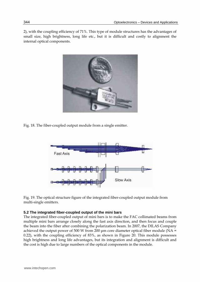
5.1 Fiber-coupled integration of single-emitters In the case of less demand for the output power, a single emitter can be directly coupled into
the fiber, as shown in Figure 18. This structure has the advantages of small size, low cost,
long life span and mature technology etc., and the output power of up to 8 ~ 10 W/module
level can be afforded by numbers of semiconductor laser suppliers currently. In the case of
high optical power requirements, the multiple collimated beams emitted from single
emitters can be used by fast axis collimators (FAC), in which the fast axis direction is packed
closely, and then the polarized beam is combined and coupled into the fiber. In 2009, the
Nlight Company integrated 14 single emitter units into a module using this structure and
obtained 100 W output power from 105 μm core diameter optical fiber (N.A. =0.15) (Figure
www.intechopen.com
Optoelectronics – Devices and Applications
344
2), with the coupling efficiency of 71%. This type of module structures has the advantages of
small size, high brightness, long life etc., but it is difficult and costly to alignment the
internal optical components.
Fig. 18. The fiber-coupled output module from a single emitter.
Fig. 19. The optical structure figure of the integrated fiber-coupled output module from multi-single emitters.
5.2 The integrated fiber-coupled output of the mini bars The integrated fiber-coupled output of mini bars is to make the FAC collimated beams from multiple mini bars arrange closely along the fast axis direction, and then focus and couple the beam into the fiber after combining the polarization beam. In 2007, the DILAS Company achieved the output power of 500 W from 200 μm core diameter optical fiber module (NA = 0.22), with the coupling efficiency of 83%, as shown in Figure 20. This module possesses high brightness and long life advantages, but its integration and alignment is difficult and the cost is high due to large numbers of the optical components in the module.
www.intechopen.com

Recent Developments in High Power Semiconductor Diode Lasers
345
Fig. 20. The integrated fiber-coupled output module from multi-mini bars.
5.3 The fiber-coupled output of the semiconductor laser array stacks packaged with micro-channel heat sink The fast and slow axis collimated beams from the multiple micro-channel heat sink packaged laser array stack are integrated spatially followed by the beam uniformization, and then focus and couple the beams into fiber, as shown in Figure 21. Currently, the output power of this module is up to 400 W with 200 μm core diameter optical fiber (N.A.= 0.22). The module with this structure has the higher brightness, less optical components and simple structure, but the cost is higher. In addition, the deionized water must be used as cooling medium, so the maintenance demand is high. Meanwhile, since the lifetime of the micro-channel heat sink is short due to the erosion of the deionized water, the lifetime of this module would be only about 20,000 hours if the elaborate cooling water management is unavailable.
Fig. 21. The integrated fiber-coupled output module from laser array stacks packaged with micro-channel heat sink.
www.intechopen.com

Optoelectronics – Devices and Applications
346
Fig. 22. The integrated fiber-coupled output module from laser array laser arrays packaged by conduction heat sink.
5.4 The fiber-coupled output of the semiconductor laser arrays packaged by conduction heat sink The beams from the multiple conductive heat sink packaged laser array are integrated spatially after the fast and slow axis collimation, and then go into the optical fiber directly through focusing and coupling system. Currently, the DILAS Company used this idea and achieved the output power of 200 W and 500 W respectively from 200 μm core diameter optical fiber module (NA = 0.22) and 400 μm core diameter optical fiber module, with the coupling efficiency of about 80%. Despite of the relatively lower brightness, compared with other structures, this type of module structures, as shown in Figure 22, has a lot of advantages, such as less optical components, simple structure, long lifetime, maintenance-free and low cost. As for the direct industrial applications using the high power and high beam quality semiconductor lasers, besides the methods mentioned above, the wavelength-beam-combining technology and the polarization-beam-combining technology can be used to obtain high power and high beam quality if the material processing is insensitive to the wavelength. It can also multiply the output power according to the number of the combining wavelengths and remain the output beam quality unchanged. In this field, the Laserline Company has the leading technologies. They integrated the micro-channel packaged cm bar stacks and achieved high output power from the level of hundreds of watts to the level of megawatts with high beam quality laser processing systems: 2000 W (BPP: 20 mm·mrad), 4000 W (BPP: 30 mm·mrad), 10000 W (BPP: 100 mm·mrad).
6. Conclusion
High power semiconductor laser diode technology is rapidly maturing technically and commercially. Laser diode prices are now low enough to intersect a broad range of commercial applications which has resulted in increased production quantities and competition. In recent years, with the rapid development of semiconductor material epitaxial growth technology, waveguide structure optimization technique, cavity surface-passivation technology, high stability packaging technology, high efficiency cooling technology, particularly driven by the demand of applications in the direct semiconductor laser industrial processing and high-power fiber laser pumping, high power, high
www.intechopen.com

Recent Developments in High Power Semiconductor Diode Lasers
347
operational temperature, high beam quality semiconductor lasers has been developed rapidly, which provide a light foundation for high-quality, high performance solid state laser pumping system, direct semiconductor laser processing equipment and high-performance high-power fiber laser pump source. Along with diode bar improvements, enhancements in the component and system design must be developed in order to handle the increased current and heat loads at these high powers. The improvement in power limits for laser diode bars will require design advancements for all of the parts of the laser diode system from a multidisciplinary team. Modularity configuration for special application requirements will certainly be a main trend of the developing high power diode lasers. Since the high power laser diode stacks of tomorrow must be looked at the diodes as a part of a large integral system, considerations such as the dimension and weight of a wire or the delivery of water must be weighed by the future designers. When these new elements are combined to form high power stacks coupled with high performance packaging and systems, they will open the doors to new market opportunities.
7. References
Crump P., Wang J., Patterson S., Wise D., Basauri A., DeFranza M., Elim S., Dong W., Zhang S., Bougher M., Patterson J., Das S., Grimshaw M., Farmer J., DeVito M. & Martinsen R. (2006). Diode Laser Efficiency Increases Enable >400-W Peak Power from 1-cm Bars and Show a Clear Path to Peak Powers in Excess of 1-kW. Proceedings of SPIE, Vol. 6104, pp.610409-1-10, ISBN, 9780819461469, San Jose, CA, USA, January 23, 2006
Du J.H., Zhou H.L., Schleuning D., Agrawal V., Morales J., Hasenberg T. & Reed M. (2008). 8xx nm kW Conduction Cooled QCW Diode Arrays with both Electrically Conductive and Insulating Submounts. Proceedings of SPIE, Vol.6876, pp.687605-1-11, ISBN 9780819470515, San Jose, CA, USA, 21 January 2008
Endriz J. G., Vakili M., Browder G. S., Devito M., Haden J. M., Harnagel G. L., Plano W. E., Sakamoto M., Welch D. F., Willing S., Worland D.P. & Yao H. C. (1992). High Power Diode Laser Arrays. IEEE J. of Quantum Electronics, Vol.28, No.4, (April 2009), pp, 952-965, ISSN 0018-9197
Fan L., Cao C. S., Thaler G., Nonnemacher D., Lapinski F., Ai I., Caliva B., Das S., Walker R., Zeng L. F., McElhinney M. & Thiagarajan P. (2011). Reliable High-Power Long-Pulse 8XX-nm Diode Laser Bars and Arrays Operating at High Temperature. Proceedings of SPIE, Vol. 7918 pp. 791805-1-7, ISBN 9780819484550, San Francisco, California, USA, January 23, 2011
Krejci M., Gilbert Y., Müller J., Todt R., Weiss S. & Lichtenstein N. (2009). Power Scaling of Bars towards 85mW per 1μm Stripe Width Reliable Output Power. Proceedings of SPIE, Vol. 7198, pp.719804-1-12, ISBN 9780819484550, San Jose, CA, USA, January 26, 2009
Lammert R.M., Oh S.W., Osowski M.L., Panja C., Qian D., Rudy P.T., Stakelon T. & Ungar J.E. (2005). Advances in Semiconductor Laser bars and Arrays. Proceedings of SPIE, Vol.5887 pp. 58870B-1-11, ISBN 9780819458926, San Diego, CA, USA August 2, 2005
Leers M., Boucke K., Scholz C. & Westphalen T. (2007). Next generation of Cooling Approaches for Diode Laser Bars. Proceedings of SPIE, Vol. 6456, pp.64561A-1-10, ISBN 9780819465696, San Jose, CA, USA, January 22-24, 2007
Li H.X., Reinhardt F., Chyr I., Jin X., Kuppuswamy K., Towe T., Brown D., Romero O., Liu D., Miller R., Nguyen T., Crum T., Truchan T., Wolak E., Mott J. & Harri J. High-
www.intechopen.com

Optoelectronics – Devices and Applications
348
Efficiency, (2008). High-Power Diode Laser Chips, Bars, and Stacks. Proceedings of SPIE, Vol. 6876, pp.68760G-1-8, ISBN 9780819470515, San Jose, CA, USA, January 21, 2008
Lichtenstein N., Manz Y., Mauron P., Fily A., Schmidt B., Müller J., Arlt S., Weiß S., Thies A., Troger J. & Harder C. (2005). 325 Watt from 1-cm Wide 9xx Laser Bars for DPSSL- and FL-Applications. Proceedings of SPIE, Vol. 5711, pp. 1-11, ISBN 9780819456854, San Jose, CA, USA, January 25, 2005
McNulty J.(2008). Processing and Reliability Issues for Eutectic AuSn Solder Joints. International Microelectronics and Packaging Society. Permission granted from the 41-International Symposium on Microelectronics (IMAPS) Proceedings, pp.909-916, ISBN 0-930815-86-6, Providence, Rhode Island, November 2-6, 2008
Müller J., Todt R., Krejci M, Manz-Gilbert Y., Valk B., Brunner R., Bättig R. & ichtenstein N. (2010). CW to QCW Power Scaling of High Power Laser Bars. Proceedings of SPIE, Vol. 7583, pp.758318, ISBN 9780819479792, San Francisco, California, USA, January 25, 2010
Puchert R., Bärwolff A., Voß M., Menzel U., Tomm J. W. & Luft J. (2000). Transient Thermal Behavior of High-Power Diode-Laser Arrays, IEEE Transaction on Components, Packaging and Manufacturing Technology, Part A, Vol.23, No. 1, (March 2000), pp. 95-100, ISSN 1521-3331
Schleuning D., Griffin M., James P., McNulty J., Mendoza D., Morales J., Nabors D., Peters M., Zhou H. L. & Reed M. (2007). Robust Hard-Solder Packaging of Conduction Cooled Laser Diode Bars. Proceedings of SPIE, Vol.6456, pp.645604-1-11, (2007) ISBN 9780819465696, San Jose, CA, USA, January 22-24, 2007
Solarz R. W., Emanuel M. A., Skidmore J. A., Freitas B. L. & Krupke W. F. (1998). Trends in Packaging of High Power Semiconductor Laser Bars. Laser Physics, Vol. 8, No. 3, (March 1998), pp. 737-740, ISSN 1729-8806
Srinivasan R., Miller R. & Kuppuswamy K. (2007). Next-Generation Active and Passive Heatsink Design for Diode Lasers. Proceedings of SPIE, Vol.6456, pp.64561D-1-10, ISBN 9780819465696, San Jose, CA, USA, January 22-24, 2007
Tu L.W., Schubert E.F., Hong M. & Zydzik G.J. (1996). In-Vacuum Cleaving and Coating of Semiconductor Laser Facets Using Thin Silicon and a Dielectric. Journal of Applied Physics, Vol. 80, No.11, (December 1996), pp. 6448-6451, ISSN 0021-8979
Vetrovec J., Feeler R. & Bonham S. (2010). Progress in the Development of Active Heat Sink for High-Power Laser Diodes. Proceedings of SPIE, Vol.7583, pp.75830K-1-8, ISBN 9780819479792, San Francisco, California, USA, January 25, 2010
Voss M., Lier C., Menzel U., Bärwolff A. & Elsaesser T. Time-Resolved Emission Studies of GaAs/AlGaAs Laser Diode Arrays on Different Heat Sinks. Journal of Applied Physics, Vol.79, No.2, (January 1996), pp.1170-1172. ISSN 1089-7550
Yanson, D., Levi, M., Shamay M., Teslera R., Rappaporta, N., Dona Y., Karnia Y., Schnitzera, I., Sicronb N. & Shustermanb S. (2011). Facet Engineering of High Power Single Emitters. Proceedings of SPIE, Vol.7918, pp.79180Z-1-12, ISBN 9780819484550, San Francisco, California, USA, January 23, 2011
Ziegler M., Weik F., Tomm J. W., Elsaesser T., Nakwaski W., Sarzala R. P., Lorenzen D., Meusel J. & Kozlowska A. Transient Thermal Properties of High-Power Diode Laser Bars. Applied Physics Letters, Vol. 89, No. 26, (December 2006), pp.3506-1-3, ISSN 1077-3118
Zweben C., (2004). New Material Options for High-Power Diode Laser Packaging. Proceedings of SPIE, Vol. 5336, pp166-175, ISBN 9780819452443, Bellingham, WA, USA, June 1, 2004
www.intechopen.com

Optoelectronics - Devices and ApplicationsEdited by Prof. P. Predeep
ISBN 978-953-307-576-1Hard cover, 630 pagesPublisher InTechPublished online 03, October, 2011Published in print edition October, 2011
InTech EuropeUniversity Campus STeP Ri Slavka Krautzeka 83/A 51000 Rijeka, Croatia Phone: +385 (51) 770 447 Fax: +385 (51) 686 166www.intechopen.com
InTech ChinaUnit 405, Office Block, Hotel Equatorial Shanghai No.65, Yan An Road (West), Shanghai, 200040, China
Phone: +86-21-62489820 Fax: +86-21-62489821
Optoelectronics - Devices and Applications is the second part of an edited anthology on the multifaced areasof optoelectronics by a selected group of authors including promising novices to experts in the field. Photonicsand optoelectronics are making an impact multiple times as the semiconductor revolution made on the qualityof our life. In telecommunication, entertainment devices, computational techniques, clean energy harvesting,medical instrumentation, materials and device characterization and scores of other areas of R&D the scienceof optics and electronics get coupled by fine technology advances to make incredibly large strides. Thetechnology of light has advanced to a stage where disciplines sans boundaries are finding it indispensable.New design concepts are fast emerging and being tested and applications developed in an unimaginable paceand speed. The wide spectrum of topics related to optoelectronics and photonics presented here is sure tomake this collection of essays extremely useful to students and other stake holders in the field such asresearchers and device designers.
How to referenceIn order to correctly reference this scholarly work, feel free to copy and paste the following:
Li Zhong and Xiaoyu Ma (2011). Recent Developments in High Power Semiconductor Diode Lasers,Optoelectronics - Devices and Applications, Prof. P. Predeep (Ed.), ISBN: 978-953-307-576-1, InTech,Available from: http://www.intechopen.com/books/optoelectronics-devices-and-applications/recent-developments-in-high-power-semiconductor-diode-lasers