1 VECSEL Semiconductor Lasers: A Path to High-Power ... · Semiconductor Disk Lasers. ... 4j1...
72
1 VECSEL Semiconductor Lasers: A Path to High-Power, Quality Beam and UV to IR Wavelength by Design Mark Kuznetsov 1.1 Introduction Since its invention and demonstration in 1960, several types of laser have been developed, such as solid-state, semiconductor, gas, excimer, and dye lasers [1]. Today, lasers are used in a wide range of important applications, particularly in optical fiber communication, optical digital recording (CD, DVD, and Blu-ray), laser materials processing, biology and medicine, spectroscopy, imaging, entertainment, and many others. A number of properties enable the application of lasers in these diverse areas, each application requiring a particular combination of these properties. Some of the most important laser properties are laser emission wavelength; output optical power; method of laser excitation, whether by optical pumping or electrical current injection; laser power consumption and efficiency; high-speed modulation or short pulse generation ability; wavelength tunability; output beam quality; device size; and so on. Thus, optical fiber communication [2], a major application that enables modern Internet, commonly requires lasers with emission wavelengths in the 1.55 mm low- loss band of glass fibers and with single-transverse mode output beams for coupling into single-mode optical fibers. Typically, a given laser type excels in some of these properties, while exhibiting shortcomings in others. For example, by using different material compositions and structures, the most widely used semiconductor diode laser [3–12] can cover a wide range of wavelengths from the ultraviolet (UV) to the mid-IR, can be advantageously driven by diode current injection, and is very compact and efficient. However, the good beam quality, that is, single-transverse mode near- circular beam operation, can be typically achieved in semiconductor lasers only for output powers below 1W. Much higher power levels are achievable from semicon- ductor lasers only with large aspect ratio highly multimoded poor quality optical beams. On the other hand, the solid-state lasers [13, 14], including fiber lasers [15], can emit hundreds of watts of output power with excellent beam quality, however, their emission wavelengths are restricted to discrete values of electronic transitions in ions, such as the classic 1064nm wavelength of the Nd:YAG laser, making them Semiconductor Disk Lasers. Physics and Technology. Edited by Oleg G. Okhotnikov Copyright Ó 2010 WILEY-VCH Verlag GmbH & Co. KGaA, Weinheim ISBN: 978-3-527-40933-4 j1
Transcript of 1 VECSEL Semiconductor Lasers: A Path to High-Power ... · Semiconductor Disk Lasers. ... 4j1...
1VECSEL Semiconductor Lasers: A Path to High-Power,Quality Beam and UV to IR Wavelength by DesignMark Kuznetsov
1.1Introduction
Since its invention and demonstration in 1960, several types of laser have beendeveloped, such as solid-state, semiconductor, gas, excimer, and dye lasers [1]. Today,lasers are used in a wide range of important applications, particularly in optical fibercommunication, optical digital recording (CD, DVD, and Blu-ray), laser materialsprocessing, biology and medicine, spectroscopy, imaging, entertainment, and manyothers. A number of properties enable the application of lasers in these diverse areas,each application requiring a particular combination of these properties. Some of themost important laser properties are laser emission wavelength; output optical power;method of laser excitation, whether by optical pumping or electrical current injection;laser power consumption and efficiency; high-speed modulation or short pulsegeneration ability; wavelength tunability; output beam quality; device size; and soon. Thus, optical fiber communication [2], a major application that enables modernInternet, commonly requires lasers with emission wavelengths in the 1.55mm low-loss band of glass fibers and with single-transverse mode output beams for couplinginto single-mode optical fibers. Typically, a given laser type excels in some of theseproperties, while exhibiting shortcomings in others. For example, by using differentmaterial compositions and structures, the most widely used semiconductor diodelaser [3–12] can cover a wide range of wavelengths from the ultraviolet (UV) to themid-IR, can be advantageously driven by diode current injection, and is very compactand efficient. However, the good beam quality, that is, single-transverse mode near-circular beam operation, can be typically achieved in semiconductor lasers only foroutput powers below 1W. Much higher power levels are achievable from semicon-ductor lasers only with large aspect ratio highly multimoded poor quality opticalbeams. On the other hand, the solid-state lasers [13, 14], including fiber lasers [15],can emit hundreds of watts of output power with excellent beam quality, however,their emission wavelengths are restricted to discrete values of electronic transitionsin ions, such as the classic 1064 nm wavelength of the Nd:YAG laser, making them
Semiconductor Disk Lasers. Physics and Technology. Edited by Oleg G. OkhotnikovCopyright � 2010 WILEY-VCH Verlag GmbH & Co. KGaA, WeinheimISBN: 978-3-527-40933-4
j1

inapplicable for applications requiring specific inaccessible wavelengths. For exam-ple, the 488 nm excitation wavelength required for many fluorescent labels inbiomedical applications [16], such as the green fluorescent protein (GFP), is notaccessible by direct solid-state laser transitions. Therefore, the 488 nm wavelengthbiomedical applications have required in the past the use of large and inefficientAr gas lasers, which serendipitously have the required emission wavelength. Thisexplains the large variety of laser types used today, where one or another type fits agiven application with its beneficial properties, while carrying the baggage of itsundesirable properties.
It is therefore useful and important to develop a laser that exhibits simultaneouslythe application required and desired laser properties, such as emission wavelength,optical power, beam quality, efficiency, compact size, and so on. Vertical-external-cavity surface-emitting laser (VECSEL) [17–24], also called optically pumped semi-conductor laser (OPSL) or semiconductor disk laser (SDL), is a relatively new laserfamily that uniquely combines many of these desirable laser properties simulta-neously, and because of this, it is becoming the laser of choice for awide range of laserapplications. This chapter describes VECSEL lasers and their history; discusses howthey aremade and characterized; explains how VECSEL structure enables their basicproperties; and indicates key applications enabled by this unique combination ofproperties. Other chapters in this book address in more detail the various aspectsand applications of this remarkable new class of lasers.
1.2What Are VECSEL Semiconductor Lasers
1.2.1History of VECSELs: Semiconductor Lasers, Optical Pumping, and External Cavity
Vertical-external-cavity surface-emitting lasers were developed in the mid-1990s[17, 18] to overcome a key problem with conventional semiconductor lasers: how togenerate watt-level and higher optical powers with fundamental transverse modecircular optical beam quality. The versatile semiconductor diode lasers are verywidely used because of their numerous advantageous properties, such as size,efficiency, electrical current laser excitation and modulation, and wide wavelengthcoverage. Using GaN, GaAs, InP, and GaSb semiconductor material systems,for example, these lasers can access 0.4, 0.8, 1.5, and 2.0 mm emission wavelengthregions. However, obtaining lasers with both high optical power and goodbeam quality simultaneously has always been a difficult task, although it is keyfor many important scientific and commercial laser applications. Such combina-tion is required, for example, for efficient nonlinear optical second harmonicgeneration [14, 25].
The conventional semiconductor lasers have two major configurations: edge-emitting [3–6] and surface-emitting lasers [9–11] (see Figure 1.1). The edge-emitting
2j 1 VECSEL Semiconductor Lasers: A Path to High-Power, Quality Beam and UV

lasers use a waveguide to confine light to the plane of the semiconductor chip andemit light from the edge of the chip (Figure 1.1a). Output beam cross section istypically about one by several microns, with the wider dimension in the plane of thechip. Such small waveguide dimensions are required for single-transverse modeoperation, but result in the asymmetric and strong angular divergence of the laserbeam. Laser output power is typically limited by the required excess heat dissipationfrom the chip active region or catastrophic optical damage at the semiconductorsurface [9, 12]. Scaling up laser output power requires wider waveguides with largerarea beams: this improves heat dissipation by reducing active stripe thermalimpedance and avoids catastrophic optical damage by decreasing beam opticalintensity. In this way, up to several hundred milliwatts of output power is achievablein a single-transverse mode waveguide configuration [9, 12]. For still wider wave-guides, of the order of a 100 mm, single-stripe edge-emitting lasers can emit tens ofwatts of output power, but the waveguide is then highly multimoded in the plane ofthe chip, and output beam is very elongated with a very large, 100: 1, aspect ratio.Multiple stripe semiconductor laser bars can emit hundreds of watts, but againwith ahighly multimoded output beam [9, 12].
In contrast, vertical-cavity surface-emitting lasers [10, 11] have laser cavity axis andemit light perpendicular to the plane of the laser chip (Figure 1.1b). Such lasers canemit circular fundamental transverse mode beam with powers up to several milli-watts and beam diameter of several microns. With circular cross section and largerbeam size, the laser output beam is also symmetrical and has much smallerdivergence than for edge-emitting lasers. Again, the required heat dissipation limitsthe output power and the scaling to higher powers demands larger active areas. Butfor output beam diameters greater than about 10 mm, laser output beam quicklybecomesmultimoded, anduniform current injection over such large areas is difficultwith edge injection through transparent contact layers. Arrays of semiconductorlasers have been a typical path to high output power [12, 25]. In short, surface-emitting lasers have good fundamental mode circular beams, but at powers ofonly a few milliwatts, while edge-emitting lasers can emit up to several hundredmilliwatts but with elliptical beam profile. For still higher powers, both laser types
Figure 1.1 (a) Semiconductor edge-emitting laser. (b) Semiconductor vertical-cavity surface-emitting laser (VCSEL).
1.2 What Are VECSEL Semiconductor Lasers j3

emit highly transverse multimoded output beams. In short, high power and goodbeam quality cannot be achieved simultaneously with conventional edge- or surface-emitting semiconductor lasers.
Two things become clear from the above description of semiconductor lasers.First, scaling up optical power to watt and higher levels with circular output beamsrequires beam diameters of tens and possibly hundreds of microns, which can besatisfied only by surface-emitting laser geometry. Second, good beam quality withfundamental transverse mode operation requires strong transverse mode controlof the laser cavity. Such transverse mode control can be provided by optical cavityelements external to the laser chip, which assure that fundamental transverse modeof the laser cavity, the desired operating laser mode, has diameter approximatelyequal to the gain region diameter. In this way we arrive to the concept of vertical-external-cavity surface-emitting laser.
When the beamdiameter of a surface-emitting laser becomes tens ofmicrons largeand the laser cavity is extended by an external optical element, the issue of laserexcitation acquires additional importance. Injecting carriers uniformly across a widearea is difficult in the traditional diode current injection [10]; this requires a thickdoped semiconductor current spreading layer. Such a doped layer has strong freecarrier absorption inside the extended laser cavity, which can degrade laser thresholdand efficiency. One possible solution to this problem is the use of optical pumping,which can inject excitation carriers uniformly across a wide area without usingintracavity lossy doped regions. Simple and efficient semiconductor diode pumplasers with multimode beams and very high powers have been developed and areavailable for pumping solid-state and fiber lasers. VECSEL lasers have been madewith both types of excitation, optical pumping and diode current injection.To emphasize their distinction from the common semiconductor diode lasers thatuse electrical pumping, optically pumped VECSELs are frequently referred to asOPSLs or optically pumped semiconductor lasers.
External optical cavity elements had been used previously with semiconductorlasers. For edge-emitting lasers, external reflectors provide a longer laser cavity forpulse repetition rate control in mode locking [27] and for inserting intracavity opticalelements, such as spectral-filtering gratings [27]. There had also been attempts tostabilize transverse modes of surface-emitting lasers using external sphericalmirrors [28].
Optical pumping of semiconductor lasers has a long history, where opticalpumping had been used not only for characterization of novel semiconductor laserstructures but also for generation of higher output powers or for short pulsegeneration. As early as in 1973, pulsed operation was demonstrated with opticallypumped edge-emitting GaAs semiconductor lasers [29]. Later, surface-emitting thin-film InGaAsP lasers [30] were used to generate gain-switched picosecond pulses inthe 0.83–1.59 mm wavelength range using dye laser pumping. Using an externaloptical cavity for pulse repetition rate and transversemode control, optically pumpedmode locking was demonstrated with a CdS platelet laser [31]. High peak power wasobserved in an external-cavity GaAs platelet laser pumped by a Ti:sapphire laser [32].
4j 1 VECSEL Semiconductor Lasers: A Path to High-Power, Quality Beam and UV

Using diode laser pumping, low-power 10mW CW operation was demonstratedwith GaAs VCSEL lasers [33]; in external cavity, however, such lasers emitted only20 mW [34]. A diode-laser-pumped surface-emitting optical amplifier was demon-strated at 1.5mmusing InGaAs–InGaAlAsmultiquantumwell structures [35]. Using77K low temperature operation and a Nd:YAG pump laser, 190mW continuousoutput power was obtained from an external-cavity InGaAs–InP surface emittinglaser [36]. In a similar configuration, an external-cavity GaAs VCSEL laser at 77 K hasdemonstrated CW output power of 700mW using a 1.8W krypton–ion pumplaser [37]. To obtain high power from a diode-laser-pumped semiconductor laser,specially designed edge-emitting InGaAs–GaAs laser structures were used to gen-erate as much as 4W average power [38, 39], however the beams were stronglyelongated with aspect ratios between 10 and 50 to 1. These works had demonstratedthe potential capabilities of the optically pumped semiconductor lasers; however, thegoal of a high-power compact and efficient diode-pumped room-temperature laserwith circular diffraction-limited beam profile had remained elusive prior to OPS-VECSEL demonstration in 1997 [17]. What enabled the appearance of the modernVECSEL lasers is the availability of sophisticated custom-designed multilayeredbandgap-engineered semiconductor structures, modern high-power multimodesemiconductor pump lasers, and thermal designs for efficient heat dissipation fromthe active semiconductor chip.
Figure 1.2 shows basic configuration of an optically pumpedVECSEL. A thin activesemiconductor chip, containing gain region and multilayer high-reflectivity mirror,is placed on a heat sink and is excited by an incident optical pump beam. Laser cavityconsists of the on-chip mirror and an external spherical mirror, which defines thelaser transverse mode and also serves as the output coupler. Typical laser beamdiameters on the gain chip range between 50 and 500 mm; VECSELs have beenmade
Figure 1.2 Optically pumped semiconductor vertical-external-cavity surface-emitting laser(VECSEL).
1.2 What Are VECSEL Semiconductor Lasers j5

with output powers ranging from 20mW to 20W and higher. Optically pumpedVECSEL can be thought of as a brightness or mode converter, converting a high-power low-qualitymultimode pump beamwith poor spatial and spectral brightnessinto a high-power high-quality fundamental transverse mode laser output beamwith the desired spatial and spectral properties. In this way an optically pumpedVECSEL is similar to solid-state and fiber lasers [13–15], which similarly act asbrightness or mode converters. Indeed, an optically pumped VECSEL can bethought of as a solid-state laser, where the gain medium, instead of the traditionalactive ions in a transparent hostmaterial, uses bandgap-engineered semiconductorstructures to achieve the desired laser absorption and emission properties. Just asevolution of semiconductor lasers to high power and good beam operation hasarrived at the VECSEL laser configuration, diode pumped solid-state DPSS lasershave arrived at the very similar solid-state disk laser configuration [40, 41], whichhas demonstrated kilowatt-level output powers. In such a solid-state disk laser, witha geometry similar to that in Figure 1.2, a thin solid-state gain medium, such as aYb:YAG crystal, with a thin-filmhigh-reflectivitymirror coating is placed directly ona heat sinkwith external sphericalmirror stabilizing the cavity transversemode anddiode optical pumping providing laser excitation. An important benefit of usingsemiconductors, in contrast to other solid-state gain media, is that the on-chipmultilayermirror can bemade of alternating different composition semiconductorlayers and can be grown in the same epitaxial growth step as the gain region itself.Externally deposited mirror on the semiconductor laser chip can also be used.Because of their similarity to the solid-state disk lasers, VECSELs have also beenreferred to as semiconductor disk lasers or SDLs. Optically pumpedVECSELs forma hybrid between traditional semiconductor and solid-state lasers, hence theinterest in these lasers has come from both of these laser communities. Forhigh-power good beam quality operation with wavelength versatility, such opticallypumped VECSEL lasers have many significant advantages compared to both thetraditional semiconductor diode lasers and the traditional solid-state lasers, in-cluding disk lasers.
1.2.2Basic Principles of Operation: VECSEL Structure and Function
Basic operating principles of VECSEL lasers are illustrated in Figure 1.3. The keyelement of the laser is the semiconductor chip, which contains both a multilayerlaser mirror and a gain region; Figure 1.3 shows the conduction and valence bandenergy levels across the semiconductor layers and explains the functions of thevarious layers. For optically pumped operation, incident pumpphotons with higherphoton energy are absorbed in separate pump-absorbing layers that also serve asthe quantumwell barriers. The excited carriers, electrons and holes, then diffuse tothe smaller bandgap quantum wells that provide gain to the optical wave, emittinglasing photons with lower photon energy. These separate pump absorption andquantum well laser emission layers allow independent optimization of the pumpabsorption and laser gain properties. For optically pumped VECSEL operation,
6j 1 VECSEL Semiconductor Lasers: A Path to High-Power, Quality Beam and UV

semiconductor layers are typically undoped, thus significantly simplifyingsemiconductor wafer growth and eliminating free carrier absorption of the dopedregions. For electrically pumped operation, p- and n-doped regions are used to forma p–n junction for diode current carrier injection, but this also results in opticallosses inside the laser cavity. A higher bandgap surface barrier window layer on thechip prevents carriers from diffusing to the semiconductor–air interface, wherethey could recombine nonradiatively and thus deplete laser gain. Optical wave ofthe laser mode back-reflecting from the on-chip laser cavity mirror sets up anintracavity standing wave inside the chip. Quantum wells have to be placed nearthe antinodes of this standing wave in order to provide efficient gain to the laser.This is the so-called resonant periodic gain (RPG) arrangement [42]; one ormore closely spaced wells can be placed near a given standing wave antinode.Typically, gain region thickness covers several periods of this laser mode standingwave.
Incident pump photons have higher energy than the emitted laser photons, thedifference of the two photon energies is the quantum defect. This quantum defect isone of themajor contributors to the overall laser operating efficiency; this pump–laserphoton energy difference, together with contributions from other lasing inefficien-cies, has to be dissipated as heat from the device active region. Heat dissipation fromthe VECSEL active semiconductor chip is provided by heat spreaders connected toheat sinks: either a soldered heat spreader below themirror structure or a transparentheat spreader above the surface window of the chip, or possibly both (Chapter 2).
Figure 1.3 Operating principles of optically pumped VECSELs.
1.2 What Are VECSEL Semiconductor Lasers j7

Good heat dissipation and heat sinking are critical for high-power operation of allsemiconductor lasers.Without these, temperature of the active regionwould rise andexcited carriers would escape thermally from the quantum wells into the barrierregion, thus depleting laser gain and turning the laser off in a thermal rolloverprocess. Such thermal rollover is typically the dominant mechanism that limitsoutput power in VECSEL lasers [43]. Smaller quantum defect produces less excessheat, but typically also implies smaller energy difference, or confinement energy,between electron and hole states in the wells and the barriers, making it easier forelectrons to escape thermally from the wells into the barriers, and thusmaking lasersmore sensitive to the temperature rise. Optimization of the quantum defect andelectron confinement energy is required for high-power room temperature deviceoperation.
Optical absorption in semiconductors is very strong for pump photon energiesabove the bandgap, of the order of 104 cm�1¼ 1 mm�1. This means that �63% ofpump light is absorbed on a single pass through 1 mm thick semiconductorabsorbing layer, 86% is absorbed in 2 mm. In most cases, single-pass pumpabsorption is sufficient; a pump-reflecting mirror can be included on the chip ifdouble-pass absorption is desired. A very simple pump-focusing optics can be used,since multimode pump light does not have a chance to diverge in a few micronsbefore it is absorbed; no depth of focus is required for pump optics and highbrightness is not required of the multimode pump sources. Compare this with�7 cm�1 absorption in Yb:YAG, a typical active medium in solid-state disk lasers.Such a thousand times weaker absorption requires a much thicker absorbingregion, 100–300 mm, and, in addition, multiple pump beam passes for efficientpump absorption, with correspondingly complex pump optics to handle divergentmultimode pump beams on multiple absorption passes [40, 41]. In an attempt toreduce quantum defect and improve efficiency in VECSEL lasers, in-well, ratherthan barrier, optical pumping has also been used for these devices [44–48]. Anotherimportant advantage of optically pumped semiconductor gain medium is itsspectrally broad absorption and hence tolerance of broad pump wavelengthvariation. Essentially, any pump wavelength is useful that is shorter than theabsorber region bandgap wavelength. Therefore, tight wavelength selection andtemperature control of pumpdiode lasers are not required, unlike the case for solid-state and fiber lasers. Diode laser pumping of VECSELs also offers fast directVECSEL modulation capability via pump laser current modulation, since VECSELsemiconductor gain medium has short, sub-nanosecond, carrier lifetimes, ascompared with microseconds to milliseconds lifetimes of typical solid-state gainmedia.
Since laser optical axis is perpendicular to the surface of the gain chip andquantum well gain layers are very thin, the single-pass optical gain is at most only afew percent. This means that external output coupling mirror transmission shouldalso be of the order of a few percent and the on-chip mirror reflectivity should be ashigh as possible, say greater than 99.9%. Intracavity losses should also be kept verylow, less than a percent, in order to maintain efficient laser operation.
8j 1 VECSEL Semiconductor Lasers: A Path to High-Power, Quality Beam and UV

1.2.3Basic Properties of VECSEL Lasers: Power Scaling, Beam Quality, and IntracavityOptical Elements
Basic configuration of VECSEL lasers enables their many key advantageous prop-erties, such as power scaling, beam quality, and laser functional versatility; in thissection, we describe these connections between VECSEL laser structure and devicefunctionality.
1.2.3.1 Power ScalingOne of the key important properties of VECSEL lasers is their output powerscalability: efficient research and commercial optically pumped devices have beendemonstrated with power levels between 10mW and 60W, a range of almost fourorders of magnitude, while maintaining good beam quality. Such efficient powerscalability is enabled by the laser mode and pump spot-size scalability on theVECSEL semiconductor laser chip. Since output power of semiconductor lasers istypically limited by heat dissipation and optical intensity-induced damage, increas-ing beam diameter in a VECSEL helps on both accounts, distributing heat andoptical power over larger beam area. For well-designed heat sinking with thinsemiconductor chips, heat flow from the laser active region into heat sink isessentially one-dimensional. Therefore, increasing beam area is essentially equiv-alent to operatingmultiple lasing elements in parallel, without changing thermal oroptical intensity regime of the individual lasing elements. In this scenario, bothoutput laser power and pump power scale linearly with the active area. VECSELshave been operated with on-chip beam diameters between 30 and 900 mm, whichscale the beam area and potentially output power by a factor of 900. For such powerscaling, the same semiconductor wafer and chip structure can be used, adjustingonly the laser cavity optics and pump laser arrangement. Optical pumpingallows simple uniform excitation of such widely scalable mode areas. In contrast,with electrical pumping, uniform carrier injection over hundreds of microns widearea is extremely difficult, typically leaving a weakly pumped region in the center ofthe active area and making power scaling of electrically pumped devices verychallenging. Direct optical coupling of pump diode chips into the VECSEL chipis possible with relatively simple pump lens arrangements; alternatively, multi-mode fiber-coupled pump diode sources can also be used. If pump power availablefrom a single pump diode is limited, multiple pump diodes can be used withmultiple pump beams incident on a single VECSEL chip from different angles.When heat dissipation from a single semiconductor chip becomes the limitingfactor, further scaling of optical power is possible by arranging multiple semicon-ductor gain chips within a single VECSEL laser cavity and reflecting the laser beamsequentially from these reflecting vertical amplifier chips [22, 49–52]. All ofthese factors combined make it possible to scale optically pumped VECSELpower by the demonstrated four orders of magnitude, and potentially more inthe future.
1.2 What Are VECSEL Semiconductor Lasers j9

1.2.3.2 Beam QualityAnother critically important property of VECSEL lasers is their beam quality:VECSELs operate with a circular beam, fundamental transverse TEM00 mode, andessentially diffraction-limited low beam divergence with M2� 1.0–1.3. Here, beamspatial quality parameter M2 [9] indicates how much faster a laser beam divergesangularly in the two transverse directions as comparedwith a single-transversemodediffraction-limited beam, which has M2¼ 1. Several factors contribute to this beamquality in VECSELs.Most important, VECSEL laser external-cavity optics defines andstabilizes the circular fundamental laser transverse mode; such optical elements andtheir stabilization effect are not available with the more conventional edge-and surface-emitting semiconductor lasers. Using pump and laser cavity optics,VECSELs have independent control allowingmatching of the pump spot size and thelaser fundamental transverse mode size. If the pump spot is too small, compared tothe fundamental mode size, laser threshold will be high because of the lossyunpumped regions encountered by the laser mode. If the pump spot is too large,higher order transverse laser modes with a larger transverse extent will be excited,causing multimode laser operation and thus degraded beam quality. Optimallyadjusted pump spot size gives preferentially higher gain to the fundamental lasermode, while giving excess loss from the unpumped regions to the spatially widerhigher order transverse modes; this stabilizes the fundamental transverse modeoperation. Large VECSEL laser beam and pump spot sizes on the chip, tens tohundreds of microns, as compared with just a few microns for edge-emittingsemiconductor lasers, contribute to the ease of alignment and thus to themechanicalstability of the VECSEL laser cavity, and thus also to the stability of its fundamentaltransverse mode operation. Such a large VECSEL beam diameter also convenientlyhas very low divergence angles, as compared with extremely fast divergence ofmicron-sized beams of the edge-emitting, and even surface-emitting, lasers.
The second important factor contributing to spatial beam quality and stability ofVECSEL lasers is the negligible thermal lensing in the thin, 2–8 mm, VECSELsemiconductor chip [22] when proper heat spreading/heat sinking is used. Thermallensing and other beam phase profile distortions are caused by thermally inducedrefractive index gradients in the laser gainmaterial. InVECSELs, thin semiconductoractive region with good heat sinking implies that optical path length thermaldistortions and hence beam profile changes and distortions are negligible. Incontrast, such thermal lensing is much stronger in solid-state lasers that requiremuch longer, hundreds of microns, gain path length. As a result, thermal lensingtypically forces optimal solid-state laser operation only within a narrow range ofpump and output powers where the thermal gradients and the resulting thermalintracavity lens produce laser mode size consistent with the pumping profile.VECSEL semiconductor lasers operate efficiently and with excellent beam qualityacross a wide range of operating power regimes from near to high above threshold.There is some trade-off between output power and beam quality in VECSELs: amultimode laser beam can better overlap the pump spot and thus produce somewhathigher output power. Thus, when a few transverse modes can be tolerated with asomewhat degraded M2� 3–4 beam parameter, VECSELs have been operated in
10j 1 VECSEL Semiconductor Lasers: A Path to High-Power, Quality Beam and UV

such regime with higher efficiency and higher output power than for single-transverse mode regime [22].
1.2.3.3 Laser Functional Versatility Through Intracavity Optical ElementsThe external optical cavity of semiconductor VECSELs, which controls the lasertransverse modes, can be viewed as mechanically cumbersome, making these lasersmore complex and requiring assembly and alignment as compared with the simpleintegrated edge-emitting and surface-emitting semiconductor lasers. On the otherhand, such an external cavity gives tremendous versatility to VECSEL deviceconfigurations and functions. Flexible VECSEL laser cavities, such as linear two-mirror cavity, three-mirror V-shaped cavity, and four-mirror Z-shaped cavity[18, 20, 49–54], allow flexible insertion of intracavity optical elements. Such in-tracavity functional elements are very difficult or impossible to use with integratedsemiconductor devices. We have already discussed one example of such extendedcavity versatility – inserting multiple gain elements in the cavity in series for powerscaling of VECSELs.
One important option allowed by the external cavity is the insertion of intracavityspectralfilters, suchasetalons [55,56],Brewster�s anglebirefringentfilters [54,57,58],volume gratings (Chapter 7) [59], or high-reflectivity gratings [60], to control longi-tudinal spectral modes of the laser and possibly to select a single longitudinal lasingmode. Tuning a birefringent filter by rotation then achieves tunable VECSELoperation; greater than 20 nm tuning range withmultiwatt output was demonstratedwith this approach [61].
VECSEL external cavity also allows the insertion of intracavity saturable absorberelements to achieve laser passive mode locking with picosecond and subpicosecondpulse generation (Chapter 6) [20]. In this case, the length of the external cavity alsoallows control of the pulse repetition rates, with rates as high as 50GHz demon-strated with short cavities [62]. External cavity optics also allows different beam spotsizes on the gain and absorber elements, which controls optical intensity of the beamspots and is typically required to achieve mode locking [20, 63, 64].
The open cavity of VECSELs allows placement of transparent intracavity heatspreaders in direct contact with the laser gain element without thermally resistivelaser mirrors in the path of heat dissipation (Chapter 2) [53, 65–68]. Since thermalmanagement is critical for high-power VECSEL operation, the possibility of usingsuch heat spreaders tremendously broadens laser design options with chip gain,mirror, and substrate materials that do not allow effective heat removal through theon-chip mirror. Another option for VECSELs allowed by the external cavity is themicrochip laser regime [69–72]. Here, an imperfectly heat-sunk semiconductorVECSEL chip produces an intracavity thermal lens that stabilizes laser transversemodes in a short external plane–plane laser cavity.
Low intracavity loss of VECSELs, combinedwith their wide gain bandwidth, allowsinsertion of intracavity absorption cells, such as gas cells, for intracavity laserabsorption spectroscopy (ICLAS) [73, 74]. Laser output spectrum then reflects theabsorption spectrum of the intracavity absorption cell. With intracavity real absorp-tion length of the order of 1m, equivalent laser intracavity absorption path length
1.2 What Are VECSEL Semiconductor Lasers j11

as long as 130 km has been produced [75], allowing sensitive measurements ofextremely weak absorption lines.
VECSEL output power coupling with only a few percent of transmission impliesthat its intracavity laser power is 20–100 times higher than the output power.Availability of such high intracavity power, together with high beam quality, allowsvery efficient nonlinear optical operation, such as second harmonic generation,by inserting nonlinear optical crystals inside the external laser cavity (Chapter 3)[14, 22, 24, 53, 54, 58, 76]. Using intracavity second harmonic generation, VECSELshave provided efficient laser output at wavelengths not accessible by other lasermaterials and techniques (Chapter 3).
Several examples discussed here show the tremendous versatility of VECSELsallowed by its external cavity and the various intracavity functional elements; theseallow VECSELs to operate in a wide variety of operating regimes with a correspond-ingly large variety of laser applications.
To summarize this section, some of the key properties of VECSELs that makethem so useful, namely, output power scaling, beam quality, and functional deviceversatility, follow from the unique structure of these devices, including semicon-ductor chip, external laser cavity, and optical pumping configuration.
1.2.4VECSEL Wavelength Versatility Through Materials and Nonlinear Optics
Oneof themost important properties ofVECSEL lasers is theirwavelength versatility:VECSELs have been made with output wavelengths ranging from 244 nm [77] and338 nm [24, 78] in the UV; through the 460–675 nm range of blue, green, yellow,orange, and red in the visible (Chapter 3) [22, 24, 52–54, 58, 79]; through the0.9–2.4 mm in the near-infrared (NIR) (Chapter 4) [18, 23, 67, 68, 80, 81]; to the 5mmin the mid-IR [82–85]. In principle, any wavelength in this range is accessible bydesign. This is simply not possiblewith any other laser type, not with the power, beamquality, and efficiency available from VECSELs. In this section, we discuss how suchwavelength versatility of VECSELs is made possible by using different semiconduc-tor materials and structures, in combination with the use of efficient nonlinearoptical conversion.
1.2.4.1 Wavelength Versatility Through Semiconductor Materials and StructuresCompound semiconductor materials have different bandgap energies, and thusdifferent photon emission wavelengths, for different material compositions. Con-trolling bandgaps of multiple layers of semiconductor structures, including thequantum well photon-emitting layers, allows control of laser emission wavelengthby design. Such bandgap control of semiconductor heterostructures is requiredfor VECSEL structures as in Figure 1.3, which also includes mirror layers, pumpabsorbing layers, and so on. Over more than 40 years of compound semiconductortechnology, several semiconductor material systems have been developed that allowreliable growth of such bandgap-engineered multilayer structures. Starting sub-strates for VECSEL structures are binary semiconductor wafers; lattice constants of
12j 1 VECSEL Semiconductor Lasers: A Path to High-Power, Quality Beam and UV

themultiple layers of an epitaxially grown structure have to be closely matched to thesubstrate to avoid large strain and the resulting growth of crystalline defects thatdestroy laser operation. Epitaxial growth of ternary, quaternary, and even quinarysemiconductor alloys has been developed, which allows independent control ofsemiconductor layer bandgap energy while maintaining lattice match to the sub-strate. Using group III–V semiconductor GaAs substrate material system with itsternary (e.g., InGaP, AlGaAs, InGaAs, GaAsP, GaAsSb), quaternary (e.g., InGaNAs,InAlGaAs), and quinary (e.g., InAlGaAsP) alloys, VECSEL lasers have been dem-onstrated with emission wavelengths in the 660–1300 nm wavelength range[18, 23, 68, 79, 86–88]. InP-based material system using quaternary alloys (e.g.,InGaAsP, InGaAlAs) allows VECSEL lasers to access the 1500–1600 nm optical fibercommunication wavelength regions [23, 80, 89–93]. Starting with GaSb substratewith ternary (e.g., GaInSb, AlAsSb) and quaternary (e.g., GaInAsSb, GaAlAsSb)alloys, VECSELs with emission wavelengths in the 2.0–2.3mm range have beendemonstrated (Chapter 4) [23, 48, 81, 94]. Recently, group IV–VI semiconductorPbTe/PbEuTe and PbSe/PbEuTe-based material systems have been used to demon-strate VECSELs in the 4.5–5 mmwavelength range [82–85]. VECSELs have also beenfabricated in the GaN/InGaN material system [95, 96], which opens the 400 nmwavelength region for direct VECSEL operation.
It is important to note that a lattice-matched semiconductor material system forVECSELs must allow not only the desired emission wavelength but also the creationof very high reflectivity on-chip Bragg mirror. To achieve such high reflectivity, highrefractive index contrast is required between the high- and low-index mirrormaterials. High index contrast is available in the GaAs material system. However,such contrast is poor in the InP material system, requiring thicker mirrors withmore layers and correspondingly larger thermal impedance, which is detrimental tolaser operation. InP material system is important because of its access to the1500–1600 nm telecom wavelength emission range. Improved VECSEL laser per-formance at these wavelengths has been achieved by bonding or fusing InP-basedgain region wafers with high-reflectivity GaAs-based Bragg mirror wafers [97, 98].No lattice matching is required for this wafer fusion approach, thus broadening thechoices available for laser emission wavelength materials and mirror materials.
Theuseofdimensionally, orquantum, confinedsemiconductor active regions [4, 8]allows further control of the VECSEL emission wavelengths. By adjusting thethickness of quantum wells (2D) or diameter of quantum wires (1D) and dots(0D), as well as the composition of confining barrier layers, the quantum-confinedelectron and hole energy levels are shifted and VECSEL designer acquires theadditional fine control of laser emission wavelength (Chapter 5) [4, 8, 18, 87, 99–102]. Using a controlled amount of strain [4, 8, 18, 87] in the quantum-confinedlight-emitting regions further expands the range of available material compositionsand thus emission wavelengths for a semiconductor material system. Thus, forexample, the strained InGaAs on GaAs material system is used very successfully forlight emission in the 950–1150 nm wavelength region [43, 68, 87].
Such diversity and flexibility of alloyed compound semiconductor material sys-tems allows designing VECSELs with direct laser emission in the wide 0.6–5mm
1.2 What Are VECSEL Semiconductor Lasers j13
wavelength range [18, 23, 79];many of these emissionwavelengths have already beendemonstrated, both in research and in commercial devices.
Semiconductor gain media, especially with engineered quantum-confined quan-tumwell and quantumdot structures, can have very large gain bandwidths, from tensto more than a hundred nanometers in wavelength [4–9]. Using intracavity tunablefilters, tunable VECSELs have been demonstrated, for example, with 80 nm near2.0mm [103], 30 nm near 1175 nm [58], 33 nm near 975 nm [51], 30 nm near 850 [66],and 10 nm near 674 nm [79]. Such tunability is useful for such laser applications asspectroscopy. At the same time, the use of intracavity tunable filters allows to setVECSEL output wavelength to a specific precise stable value required for a givenapplication. This ability to set VECSEL output wavelengths has proven very valuablein certain applications, such as exciting marker fluorescent proteins in biologicalimaging applications, where specific excitation wavelengths, for example, 488 nm,are most efficient for a given marker protein [16]. Using intracavity filters, VECSELshave also been operated in the single longitudinal mode, or single-frequencyregime [104], important for some applications, such as spectroscopy. In this way,VECSELs, by design, access not only a wide output wavelength range but also veryspecific desired wavelengths at arbitrary locations within that range.
An optically pumped laser is not very useful if a suitable pump laser is not easilyavailable; this is frequently the case with solid-state lasers, which require pump laserswith a very narrow, only several nanometerswide, range of pumpingwavelengths. Animportant factor thatmakes the wideVECSEL emissionwavelength range possible isthe wide pump wavelength range, tens to hundreds of nanometers wide, allowed byoptically pumped VECSELs. In practice, this means that a desired emission wave-length can be achieved inVECSELswhile usingwidely available efficient pumpdiodelasers at commonly available pump wavelengths. For example, the 808 nm wave-length pump lasers, the standard pumping wavelength for Nd:YAG solid-state lasersand thus wavelength where pump diodes are easily available, have been used forVECSEL lasers emitting in the 920–1300 nm wavelength range [18, 67, 68, 87]. Thecommon 980 nm pump lasers, the standard wavelength for pumping Er-doped fiberamplifiers, have been used to pump 1550 nmVECSELs [97]. Pump lasers at 790, 808,830, and 980 nm have been used to pump 2.0–2.3mm lasers [81, 94, 105, 106]. Pumpwavelength of 1.55 mmhas been used for pumping 5mm lasers [82–85]. Thus, pumpwavelength versatility is an important contributor to the emission wavelengthversatility in VECSELs.
1.2.4.2 Wavelength Versatility Through Nonlinear Optical ConversionPerhaps the biggest contributor to thewavelength versatility ofVECSEL lasers, aswellas to their commercial success so far, has been efficient nonlinear optical conversionpossible with VECSELs. Nonlinear optical conversion uses a nonlinear optical crystalto generate light at harmonics, as well as sum or difference frequencies of theincoming light beams (Chapter 3) [14, 24, 25]. The most common is the secondharmonic generation SHGprocess, where light is generated at twice the frequency orhalf the wavelength of the fundamental laser emission. For example, a very useful488 nmwavelength visible blue output can be produced as a second harmonic of the
14j 1 VECSEL Semiconductor Lasers: A Path to High-Power, Quality Beam and UV

fundamental 976 nm near-infrared laser emission. The nonlinear optical processescan be further cascaded to generate third, fourth, and so on harmonics of thefundamental input light frequency. Using this approach, fundamental wavelengthsin the near-infrared between 0.8 and 1.3 mm, which are more readily accessibledirectly by semiconductor VCSELS, have been converted efficiently to the0.24–0.65mm ultraviolet and visible, including blue, green, yellow, orange, and red,wavelength range (Chapter 3) [22, 24, 53, 54, 57, 58, 78]. Nonlinear optical conversionhas tremendously broadened thewavelength range accessible byVECSELs andmadeefficient light sources available at wavelengths that previously had been accessibleonly by inefficient gas lasers, such as Ar laser at 488 nm for fluorescent markerapplications, or where no effective light sources had been available at all, such as577 nmyellowwavelength for photocoagulation treatment in ophthalmology [57, 58].
Efficient nonlinear optical conversion requires high optical intensity; this isprovided by high optical power and good beam quality, which allows focusing laserbeam to small diameters. High optical power and good beam quality are precisely thefundamental properties of VECSEL lasers, which make them very efficient sourcesfor nonlinear optical conversion. The efficiency of nonlinear optical conversionincreases with the increase in optical intensity. Even though the fundamental outputpower of VECSELs is high, their intracavity power is still much higher. With typicaloutput coupling mirror in VECSELs having a transmission of between 1 and 5%,intracavity laser power is remarkably 20–100 times higher than the output power.Thus, a 20Woutput power VECSEL with output coupling transmission of 0.7% hasan intracavity power of 2.8 kW [107], while beam quality M2� 1.1 is also very high.Such high VECSEL intracavity powers allow the use of very efficient intracavitynonlinear optical conversion (Chapter 3) [14, 24, 25], which because of the higherintracavity power can be much more efficient than similar conversion done outsidethe laser cavity. For intracavity SHG, for example, a nonlinear optical crystal isinserted inside the laser cavity and a dichroic laser output mirror has 100%reflectivity at the fundamental laser wavelength and 100% transmission at thesecond harmonic frequency; laser cavity output is then emitted at the secondharmonic frequency (Chapter 3). Such nonlinear optical processes can be furthercascaded inside the laser cavity to produce third and fourth harmonic laser out-put [108], producing, for example, 355 nm third harmonic UV radiation from thefundamental 1065 nmnear-infrared laser emission. Alternatively, intracavity-doubledlaser output can then be further doubled in frequency outside the laser cavity; in thisway, 244 nm UV output has been produced from the 976 nm fundamental laserwavelength [77].
Another approach to extend wavelengths accessible by VECSEL lasers is to operatethese lasers in a dual wavelength mode with intracavity nonlinear optical sum ordifference frequency generation [109–113]. Also possible is intracavity sum frequen-cy generation in a VECSEL laser with externally injected solid-state laser beam [114].Using such intracavity difference frequency generation, VECSEL laser becomesa room temperature source of 4–20 mm wavelength mid- to far-infrared radiation.Still longerwavelength terahertz radiation, 0.1–2.0 THz or 150–3000mmwavelength,can be generated using short-pulse mode-locked VECSELs [115]. In this approach,
1.2 What Are VECSEL Semiconductor Lasers j15

very short 260–480 fs optical pulses incident on a photoconductive antenna produceterahertz radiation with bandwidth inversely proportional to the pulse width. Asimilar short pulse-driven photoconductive antenna is used for time domaindetection of the terahertz radiation [115].
In summary, VECSEL lasers can access an extraordinarily wide range of wave-lengths from the UV, through the visible and near-infrared, to mid- and far-infrared,and even to the terahertz frequency range. Two key factors are the source of such awide wavelength range: flexibility of semiconductor material systems and structuresin combination with nonlinear optical conversion techniques. More important, incontrast with other laser systems, such as gas- and solid-state laser systems, whichemit only at discrete wavelengths of existing electronic transitions of active ions,semiconductor VECSELs can generate light by design within this wide range atessentially arbitrary specific target wavelengths required for different applications.
1.3How Do You Make a VECSEL Laser
Now that we have described what VECSEL lasers are, their basic operating principlesand fundamental properties that make them so uniquely useful, in this section weoutline the key elements in designing and making VECSELs. First, we describe thedesign of basic building blocks of VECSELs, see Figures 1.2 and 1.3: gain medium,on-chip Braggmirror, laser optical cavity, and optical pumping arrangement. Finally,we describe VECSEL laser characterization. Note that here we describe the designprinciples of the more common optically pumped version of VECSELs; the electri-cally pumped VECSEL is described in detail in Chapter 7 of this book; the twodifferently pumped versions sharemost of the designprinciples that are not related topumping.
1.3.1Semiconductor Gain Medium and On-Chip Bragg Mirror
The main component of VECSEL lasers is the semiconductor laser chip, whichincludes the semiconductor gain medium and the laser-cavity multilayer Braggmirror. First, we address the design of the semiconductor gain medium; this will tellus the key design and operational parameters of VECSEL lasers: the required gainlevel and number of quantum wells, laser mirror reflectivities required, laserthreshold and operational pump powers, and laser output power and efficiency.We then describe the semiconductor mirror design and show an example of a fullVECSEL semiconductor wafer structure.
1.3.1.1 Semiconductor Gain Design for VECSELsTo model VECSEL lasers, we use a simple analytical phenomenological model ofsemiconductor quantum well gain, which then gives us a very useful analyticaldescription of VECSEL laser design and operation [18]. The model here does not
16j 1 VECSEL Semiconductor Lasers: A Path to High-Power, Quality Beam and UV

include thermal considerations, which are very important in the laser design and areconsidered in detail in Chapter 2 of this book .
Semiconductor quantum well gain g, cm�1, has an approximately logarithmicdependence on well carrier density N, cm�3,
g ¼ g0 lnðN=N0Þ; ð1:1Þwhere g0 is the semiconductor material gain parameter and N0 is the transparencycarrier density. VECSEL laser threshold condition states that intracavity optical fieldis reproduced upon a round-trip inside the cavity:
R1R2Tloss expð2CgthNwLwÞ ¼ 1; ð1:2Þwhere R1 and R2 are the cavity mirror reflectivities, Tloss is the transmission factordue to round-trip cavity loss, gth is the threshold material gain, Nw is the number ofquantum wells in the gain medium, and Lw is the thickness of a quantum well.Longitudinal confinement factor C [116] of this resonant periodic gain structurecharacterizes overlap between the intracavity optical standing wave and the quantumwells spaced inside the active region. Carrier density N below threshold can becalculated from the incident pump power Pp:
N ¼ gabsPp
hnpðNwLwApÞ tðNÞ: ð1:3Þ
Here gabs is the pump absorption efficiency, hnp is the pump photon energy, Ap isthe pump spot area, and t is the carrier lifetime. Carrier lifetime is given by
1tðNÞ ¼ AþBNþCN2; ð1:4Þ
where A, B, and C are the monomolecular, bimolecular, and Auger recombinationcoefficients. From Eqs (1.1)–(1.4), we derive simple expressions for the thresholdcarrier density Nth and the threshold pump power Pth:
Nth ¼ N0ðR1R2TlossÞ�ð2Cg0NwLwÞ�1
; ð1:5Þ
Pth ¼ NthhnðNwLwApÞgabstðNthÞ : ð1:6Þ
VECSEL output power is then given by
Plas ¼ ðPp�PthÞgdiff ; ð1:7Þwhere laser differential efficiency gdiff is
gdiff ¼ goutgquantgradgabs: ð1:8Þ
The components of the differential efficiency are the output efficiency gout:
gout ¼lnðR2Þ
lnðR1R2TlossÞ ; ð1:9Þ
1.3 How Do You Make a VECSEL Laser j17

where R2 is the laser output mirror reflectivity; the quantum-defect efficiency gquant:
gquant ¼lpump
llaser; ð1:10Þ
given by the ratio of pump lpump and laser llaser wavelengths; and the radiativeefficiency grad:
grad ¼BNth
AþBNth þCN2th
: ð1:11Þ
To illustrate laser design and operation, we choose typical material and laserparameter values for a�1 mm emission wavelength InGaAs/GaAs optically pumpedVECSEL laser, as summarized in Table 1.1. Figure 1.4 shows the interplay betweenthe laser design and operational parameters, as calculated using the above model.Figures 1.4a and b show the threshold pump power and laser output power,respectively, as a function of the number of quantum wells in the structure forseveral external mirror reflectivities Rext¼R2. Because quantum wells are so thin,only�8 nm, they provide only a small amount of gain to an optical wave propagatingnormal to the plane of the well. With on-chip mirror reflectivity of 99.9%, typicaloutput coupling mirror reflectivities need also be high and range between 96 and99%; intracavity laser loss is assumed here to be 1%. Multiple wells are required forlasing, with approximately 5–15 wells minimizing laser threshold depending on theoutput mirror reflectivity. Lower output mirror reflectivity provides higher outputcoupling but has higher threshold and requires larger number of quantum wells foroperation.With 100mmpump spot size here, threshold pumppowers range between100 and 300mW. For smaller number of wells, threshold power rises very rapidly,whereas for larger number of wells, the threshold increases only slowly.
Table 1.1 Laser and material parameters used in the OPS-VECSEL laser threshold and outputpower calculations.
Parameter Description Value Units
g0 Material gain coefficient 2000 cm�1
N0 Transparency carrier density 1.7� 10þ 18 cm�3
C RPG longitudinal confinement factor 2.0 —
Lw Quantum well thickness 8.0 nmR1 On-wafer mirror reflectivity 0.999 —
Tloss Round-trip loss transmission factor 0.990 —
llaser Laser wavelength 980 nmlpump Pump wavelength 808 nmdpump Pump spot diameter 100 mmgabs Pump absorption efficiency 0.85 —
A Monomolecular recombination coefficient 1.0� 10þ 7 s�1
B Bimolecular recombination coefficient 1.0� 10�10 cm3 s�1
C Auger recombination coefficient 6.0� 10�30 cm6 s�1
18j 1 VECSEL Semiconductor Lasers: A Path to High-Power, Quality Beam and UV

Figure 1.4 Calculated characteristics of the OPS-VECSEL lasers. (a) Threshold pump powerversus the number of quantum wells. (b) Maximum output power versus the number of quantumwells. (c) Output power versus input power.
1.3 How Do You Make a VECSEL Laser j19

Figure 1.4b shows the calculated output laser power as a function of the number ofquantum wells in the structure for several different external mirror reflectivities; thecalculation assumes pump power of 1800mW. Output power is maximized above650mW for the number of wells greater than 8–10 and external mirror reflectivitiesof 96–97%. Figure 1.4c shows the calculated output power of the laser as a function ofthe input pump power. Lower external mirror reflectivity increases output slopeefficiency at the expense of the higher laser threshold.
Note that threshold power, Eq. (1.6), scales linearly with the pump, and laser, spotarea; thus smaller pump spot areas are desired for lower thresholds. However,thermal impedance between VECSEL active region and heat sink increases with thedecrease in pump area (Chapter 2), which leads to increasing active region tem-peratures, with the corresponding decrease in semiconductor gain and increase inlaser threshold for such smaller pump areas. VECSEL lasers should be designedwiththe target output power in mind, and thus with approximate pump and thermal loadlevels. Given these power levels, pump spot size should be minimized such thatthermal impedance and temperature rise are not too high; the number of quantumwells is then optimized for lower thresholds, and the output coupling mirror isoptimized for highest output power at the available pump levels.
Here we have described a simple phenomenological analytical model of thesemiconductor VECSEL; this model is useful to describe very simply and quicklythe basic design and scaling principles of VECSELs, such as the number of quantumwells required, threshold pump levels and output power levels, output couplingoptimization, and so on. This laser gain and power model should then be coupledwith thermal models of VECSELs (Chapter 2) to define device thermal impedanceand the desired pump/mode spot sizes, temperature rise of the active region, and thedesign wavelength offsets of the material photoluminescence PL peak and variouscavity resonances [18]. Alternatively, detailed numerical microscopic models ofsemiconductor lasers can be used [117, 118]. Suchmodels predict gain and emissionproperties of semiconductor materials without resorting to phenomenologicaldescription with adjustable model parameters; however such models are muchmore complex.
Multiple quantum wells required for laser gain are placed at the antinodes of thelaser optical field standing wave, with none, one, or more closely spaced wells at eachantinode, see Figure 1.3. Pump absorbing regions form the space between theantinodes. The number of quantumwells at the different antinodes is chosen such asto produce uniform quantum well excitation from the pump power that decaysexponentially from the wafer surface as it is absorbed in the semiconductor. Placingquantum wells at the laser field antinodes resonantly enhances gain in this resonantperiodic gain structure, as described by the confinement factor C. Such resonantperiodic gain arrangement effectively eliminates spatial hole burning of the lasergain medium and enables simple single-frequency operation of these lasers, bothwith [55, 104] and sometimes without [119, 120] intracavity spectral filtering.Resonant gain enhancement, however, narrows the otherwise broad spectral band-width available from the laser gain medium. Such broad spectral bandwidth isdesired, for example, for tunable laser operation or for ultrashort pulse generation. In
20j 1 VECSEL Semiconductor Lasers: A Path to High-Power, Quality Beam and UV

this case, quantum wells can be displaced from their antinode positions in thestructure to provide larger gain bandwidth at the expense of lower gain enhancementthat comes with the lower confinement factor C [18]. Another structural factor thataffects VECSEL gain bandwidth is the etalon formed between the on-chip lasermirror and the residual reflectivity at the chip surface. When this etalon is resonant,gain bandwidth is narrowed, laser gain is enhanced, and laser threshold is lowered.Designing this etalon to be antiresonant enhances gain bandwidth at the expense ofthe lower gain [20, 74].
In semiconductor lasers, strained quantum wells are frequently used, bothbecause this allows access to a larger range of laser wavelengths and because ofthe improved operating characteristics of strained quantumwell lasers [4, 8], such aslower threshold and improved temperature dependence. Because a large numberof strained quantum wells are typically used in a VECSELwafer structure, their totalthickness can easily exceed the Matthews and Blakeslee strain critical thicknesslimit [4, 8], leading to strain relaxation via crystalline defect formation, which destroyslaser operation because of strong nonradiative recombination at such �dark line�defects. Strain compensation [8, 18] must be used in this case, where layers ofsemiconductor material with the opposite sign of strain are introduced near thestrained quantum wells such as to balance out net strain in the wafer structure. Forexample, compressively strained InGaAs quantum wells on GaAs are commonlyused for�1mm laser emission. Here, usingmore than three strained quantumwellsin the laser structure exceeds the critical thickness limit and requires straincompensation; tensile-strained GaAsP layers are typically used for strain compen-sation in this material system. Reliable semiconductor VECSEL operation has beenobtained with such strain-compensated wafer structures [18] with over 35 000 h oflifetime data [54]. Using quantum dots in the laser active layers (Chapter 5) [99–102],instead of quantum wells, can provide further laser advantages, such as increasedmaterial gain bandwidth and improved temperature dependence [101]. VECSELlasers utilizing quantum dot active regions are described in detail in Chapter 5.
1.3.1.2 On-Chip Multilayer Laser Bragg MirrorThe second critical component of the VECSEL semiconductor chip is the multilayerBragg mirror that serves as one of the mirrors of the laser cavity, see Figures 1.2and 1.3. As we have seen from the laser designs in Figure 1.4, on-chip laser mirrorreflectivity should be very high, of the order of 99.9%, to keep laser thresholds low andoutput differential efficiency high. Since this mirror also forms a thermal barrierbetween the active region and the heat sink, another requirement is that mirrorthermal impedance be low so that the active region has its heat dissipated efficientlyand its temperature rise is limited. To produce efficient on-chip mirrors, multiplequarter-wave layer pairs of semiconductor materials with a high refractive indexcontrast are required. This yields high reflectivity with fewest layer pairs and thuslowest thickness and thermal impedance; good thermal conductivity of the mirrormaterials is also important. In addition, mirror materials should be nonabsorbing atthe laser and, possibly, pump wavelengths. For optically pumped VECSELs, themirror layers can be undoped, which significantly simplifies their epitaxial growth;
1.3 How Do You Make a VECSEL Laser j21

electrically pumped VECSELs require complex doping profiles in the mirror layers(Chapter 7). To achieve more efficient pump absorption in the pump absorbingregions, a pump light reflectingmirror can be includedwith the on-chip lasermirror;this, however, detrimentally increases the overall mirror thermal impedance. Higherthermal impedance of the on-chip laser mirrors can be counteracted somewhat byusing front-side transparent heat spreaders (Chapter 2).
In the GaAs material system near 1mm wavelength, high index contrast lattice-matched mirror materials, GaAs and AlAs, are available; a 30-pair mirror of suchmaterials has the desired reflectivity with the mirror thickness of about 4.5mm [18].In contrast to GaAs, InP material system near 1.55mm does not have such highcontrast materials available; the InGaAsP/InP mirrors here require 48 quarter-wavepairs to achieve the desired reflectivity [121], with the resulting higher thermalimpedance and significantly lower demonstrated output powers. Several alternativeshave been explored for improved mirrors in this case. Metamorphic, or non-lattice-matched, semiconductor mirror materials have been used, for example, GaAs/AlAsmirrors on InP substrate, as well as hybrid metal-enhanced metamorphic mir-rors [122, 123]. Dielectric mirrors [124] have also been used in VECSELs with opticalpumping since no current injection is required in this case. But metamorphic anddielectricmaterials have poor thermal conductivity and suchmirrors still have higherthan desired thermal impedance. A novel way to overcome this material limitationis to use wafer fusion [97, 98]. In this approach, lattice-matched laser mirrors aregrown on one substrate in a semiconductormaterial systemwith available high indexcontrast materials, while the gain medium is grown on a different substrate inanother material system with the desired output wavelength range. The laser mirrorand laser gain wafers with different lattice constants are then fused together; this isagain much simpler for optically pumped structures where no current injection isrequired across the fusion interface. A dramatically improved output power perfor-mance, from 0.8 to 2.6W CW, of 1.3 and 1.57 mmVECSELs was demonstrated usingsuch an approach with InP-based gain wafer fused with GaAs/AlAs-based mirrorwafer [97, 98].
1.3.1.3 Semiconductor Wafer StructureFigure 1.5 shows an example of the full semiconductor window-on-substrate waferstructure of a 980 nm VECSEL. It follows the design principles outlined above andhas been used in the first demonstration of high-power VECSEL lasers [18]. Startingfrom GaAs substrate, first the output window and then the gain region are grown,followed on top by the on-chip Bragg mirror structure. The active region contains14 In0.16Ga0.84As quantumwells of 8.0 nm thickness with 1.15% compressive strain.Each quantumwell is paired with a 25.7 nm thick GaAs0.90P0.10 strain compensatinglayer with 0.36% tensile strain such that the net averaged strain of the structure iszero. These strain-compensated quantum wells are placed at the consecutive anti-nodes of the laser standing wave using Al0.08Ga0.92As spacers that serve as pumpabsorbing layers and are designed for optical pumping at 808 nm. High-reflectivityBragg mirror at the top of the structure consists of 30 pairs of Al0.8Ga0.2As/GaAsquarter-wave thick mirror layers. The total mirror thickness is 4.5mm and it has a
22j 1 VECSEL Semiconductor Lasers: A Path to High-Power, Quality Beam and UV

thermal impedance of 21� KW�1 for a 100� 100mm2 laser spot size [18]. VECSELsemiconductor wafer structures require very good epitaxial growth control of thelayer compositions, thicknesses and strains; such control is available with themodernmetal-organic vapor-phase epitaxy (MOVPE) [18, 57, 125, 126] andmolecularbeam epitaxy (MBE) [127–129] semiconductor growth techniques.
Optically pumped VECSELs require very little processing after wafer growth; nolithographic processing is required. To use such semiconductor chip in a laser, it isfirst metallized, thinned, and soldered mirror side down onto a diamond heatspreader; subsequently, the thinned GaAs substrate is removed by selective wetchemical etching [18, 130] and the exposed window surface is antireflection (AR)coated. This AR coating serves to eliminate pump reflection loss at the OPS chipsurface. It also strongly reduces chip surface intracavity reflection at the laserwavelengths, thus weakening the subcavity etalon formed by the on-chip mirrorand the surface reflection, which otherwise can limit tuning bandwidth of the laser.This AR coating can also be made with semiconductor layers grown epitaxially onthe semiconductor wafer together with the other structure layers [107]. Diamondheat spreader with the soldered OPS chip is in turn soldered onto a thermoelec-trically temperature-controlled heat sink. Copper heat sink is typically used;however, using diamond in place of copper heat sink [107] can further decreasethe chip thermal impedance, limit its temperature rise, and produce higher outputpowers.
The VECSEL window-on-substrate wafer layer arrangement leaves no extraneoussubstrate material, with its excess thermal impedance, between the mirror and heatspreader and gives excellent high-power laser operation. An alternative is themirror-on-substrate wafer structure, where mirror layers are grown first on the substrate,
Figure 1.5 Semiconductor wafer structure of a 980 nm InGaAs/GaAs VECSEL laser.
1.3 How Do You Make a VECSEL Laser j23

followed by the active region and the output window [18]. Such mirror-on-substratestructures require back side substrate thinning, metallization, and soldering to heatsink. Handling thin semiconductor chips is very difficult; as a result, the residualsubstrate thickness is 15–30 mm with the corresponding thermal impedance andsevere limitation to high-power laser operation [18]. Using front side transparentheat sinks with such structures, using materials such as sapphire [65], siliconcarbide SiC [66], or single-crystal diamond [67], is very effective in addressing thethermal impedance problem and has demonstrated high-power laser operation(Chapter 2) [131].
1.3.2Optical Cavity: Geometry, Mode Control, and Intracavity Elements
We next outline external optical cavity configurations used for VECSEL lasers; otherthan on-chip laser mirror, optical elements forming these cavities are external to thelaser chip. VECSEL optical cavities allow control of the laser fundamental transversemode operation as well as the insertion of various intracavity elements: saturableabsorbers for laser passivemode locking, optical filters for laser wavelength selectionand tuning, nonlinear optical crystals for intracavity second harmonic generation,and so on. Such optical cavities also allow combining of multiple gain elements inseries for higher-power laser operation.
VECSEL lasers were first demonstrated with simple twomirror cavities [18, 65], asillustrated in Figures 1.2 and 1.6a. Later, as additional optical functional elementswere added to the lasers, more complex three-mirror V-shaped cavities emerged.In one version of the V-shaped cavity, as illustrated in Figure 1.6b, the OPS gain chipserves as one end mirror of the cavity [57, 66, 97, 132], with the laser output takenvariously either through the other end mirror [66, 97] or through the foldingmirror [57, 132] of the cavity. In another version of the V-shaped cavity, as illustratedin Figure 1.6c, the OPS gain chip serves as the folding mirror in the middle of thecavity [20, 62, 133]. Four-mirror Z-shaped cavities, as shown in Figure 1.6d, give evenmore flexibility in placing intracavity functional elements and manipulating laserbeam size at these elements [53, 131, 134]. Even more complex multimirror cavitieshave been usedwith two (Figure 1.6e) [49, 50] and three (Figure 1.6f) [135] active OPSgain chips in the cavity. Going beyond the above linear cavity configurations, a planarring cavity has been used for a passivelymode-locked VECSEL [136], and a nonplanarring laser cavity has been used for a VECSEL-based ring laser gyro [137]. A diffractiveunstable optical resonator has also been used with VECSELs where Gaussian beamoutput was extracted from a hard-edged outcoupling aperture [138].
A two-mirror, stable, plane–curved optical cavity (Figure 1.6a) [139] of length Lcand with curved mirror radius Rc has fundamental TEM00 laser mode beam 1/e2
diametersw1 on the planar semiconductor chip andw2 on the output sphericalmirrorgiven by
w21 ¼ 4llaserLc
p
ffiffiffiffiffiffiffiffiffiffiffiffiffiffiffiffiffiffiffiffiffiffiffiffiðRc�LcÞ=Lc
p; ð1:12Þ
24j 1 VECSEL Semiconductor Lasers: A Path to High-Power, Quality Beam and UV

w22 ¼ 4llaserRc
p
ffiffiffiffiffiffiffiffiffiffiffiffiffiffiffiffiffiffiffiffiffiffiffiffiLc=ðRc�LcÞ
p: ð1:13Þ
Figures 1.7a and b illustrate variation of the lasermode diameters on the two cavityend mirrors as a function of the cavity length. Mode diameters on the chip between100 and 200 mmcan be easily achieved in this simple cavity for cavity lengths less than
Figure 1.6 VECSEL laser cavities. (a) Two-mirror linear cavity. (b) Three-mirror V-shapedcavity for second harmonic generation (SHG).(c) Three-mirror V-shaped cavity for
passive mode locking. (d) Four-mirrorZ-shaped cavity. (e) VECSEL cavity with two gainchips. (f) VECSEL cavity with three gain chips.
1.3 How Do You Make a VECSEL Laser j25

25mm. Pump spot size should be of the order of the laser mode size on the chip toprovide efficient gain aperturing for fundamental transverse mode selection. Suchtwo-mirror cavity VECSEL lasers have also been operated in unstable resonatorregime with cavity lengths longer than mirror radius of curvature [18]. In this case,laser transversemode is stabilized by gain aperturing with strong optical loss outsidethe pumped spot on the chip.
Figure 1.7 Mode spot 1/e2 diameters of the planar–spherical cavity (a) on the semiconductor chipw1 and (b) on the output spherical mirror w2 for spherical mirror radii of curvature of Rc¼ 25 and50mm and llaser¼ 980 nm.
26j 1 VECSEL Semiconductor Lasers: A Path to High-Power, Quality Beam and UV

Another compact version of the two-mirror VECSEL cavity is the microchip laserconfiguration [69–71, 140], where a short plane–plane laser cavity is transverse modestabilized by a thermal lens formed in the gainmedium due to temperature gradientswithin the pump spot. Here, intracavity diamond heat spreader was used, with itsplanar outer surface coated with high-reflectivity output couplingmirror [70]; on-chipmirror is the second mirror of the cavity. Such arrangement allows very compactcavities; array laser operation was demonstrated for such microchip VECSELs [70].Since thermally optimized VECSEL chip mounting, with on-chip mirror soldered onheat sink without intervening substrate, produces negligible thermal lensing [22], formicrochip laser operationsufficient thermal impedance bydesign is requiredbetweentheVECSEL chip and theheat sink.MicrochipVECSELsoperate optimally onlywithina well-defined window of pump powers and pump spot sizes. Intracavity thermal lensandamicrochipmodeof laser operationare alsoused in electrically pumpedVECSELs(Chapter 7). Another version of a compactmicrochipVECSEL laser cavity doesnot relyon thermal lensing in the semiconductor, but instead uses spherical microlenses, ormicromirrors, etched directly into outer surface of diamond heat spreaders in contactwith the OPS chip surface [141–144]; arrays of such microchip lasers have also beendemonstrated [143]. A potential compact laser cavity for VECSELs is the single-transverse mode optical resonator cavity [145], where shaping of the nonplanarresonatormirror canmake all higher order transversemodes fundamentally unstable.Unlike other optically pumped VECSEL laser implementations, this resonator wouldrequire some lithographic processing of the semiconductor chip.
Inserting additional intracavity functional optical elements in theVECSEL typicallyrequires additional mirrors for the laser cavity. Thus, a three-mirror V-shaped lasercavity was used for VECSEL passive mode locking [62], as in Figure 1.6c, with a flatSESAM semiconductor saturable absorber mirror at one end of the cavity, OPS gainchip as the foldingmirror in themiddle of the cavity, and a spherical output couplingmirror at the other end of the cavity. This cavity was only 3mm long and demon-strated mode locking at 50GHz high pulse repetition rate. The V-shaped laser cavityarrangement also allows controlling relative mode spot sizes on the gain andsaturable absorber elements, with saturation intensity conditions of passive modelocking typically requiring smaller beam area on the absorber than the gain element(Chapter 6) [20].
An important enabling spatial flexibility of VECSEL laser cavities is the ability toinject pump light at various angles to the OPS chip without concern for pump beamdivergence or specific beam angle. Thus, for passivemode locking in Ref. [62], pumpbeam was injected at 45� to the chip with incident beam direction in the planeperpendicular to the plane of the picture in Figure 1.6c. This pump flexibility isenabled by the thin disk nature of the laser gain medium with pump absorptionlength of the order of only 1mm. A similar three-mirror V-shaped laser cavity(Figure 1.6b) is used extensively for VECSELs with intracavity second harmonicgeneration [57, 97, 132]. A four-mirror double-folded Z-shaped laser cavity withintracavity optical elements, such as the one shown in Figure 1.6d, has been used, forexample, for VECSELs with intracavity second harmonic generation [88] and forpassively mode-locked VECSELs [20].
1.3 How Do You Make a VECSEL Laser j27

Open multimirror cavities allow convenient insertion of intracavity optical ele-ments. As shown in Figure 1.6c, for second harmonic generation [57], an intracavitybirefringent filter is used for longitudinal mode, or wavelength, control and anintracavity nonlinear optical crystal is used for second harmonic generation. Severaltypes of intracavity frequency-selective filters have been used for VECSEL laserfrequency control, such as etalons [146], birefringent filters [104], volume Bragggratings (Chapter 6) [59], and high-reflectivity gratings [60]. Such frequency-con-trolled VECSELs have demonstrated single-frequency laser operation with linewidthbelow 5 kHz [104].
Scaling VECSELs to very high output power levels can be accomplished byovercoming some of their thermal limitations with the use ofmultiple gain elementsin series inside amore complex laser cavity, asfirst proposed inRef. [18]. Two opticallypumped semiconductor gain elements have been connected in series in the five-mirror VECSEL cavity illustrated in Figure 1.6e [50], producing 19W CWat 970 nm.Two gain chips have been used in a four-mirror cavity for high-power generationin Refs [49, 147]. Scalable optically pumped two-, three-, and four-chip cavities of thetype shown in Figure 1.6f have been used to generate as much as 66W CW at thefundamental wavelength of 1064 nm and as much as 30W CW at the secondharmonic 532 nm green wavelength [135]. In order for such multielement VECSELoptical cavities to be practical, they must be stable to component and alignmentperturbations as well as to long-term aging and drift; design of such dynamicallystable cavities has been described in Ref. [52].
Power scaling ofVECSELs typically requires largemodediameters on the gain chipto reduce device thermal impedance. A simple two-mirror cavity would need to bevery long to achieve such large mode diameters, while a compact laser cavity isdesirable. The design of such compact miniaturized cavities using Keplerian orGalilean telescopes to expand lasermode size has been described in Ref. [52]. A large480 mm diameter mode size has been demonstrated in a small 8 cm footprintKeplerian telescope folded cavity, with 531 nm green laser TEM00 output power inthe 10–20W CW range [52]. A Galilean telescope folded cavity also demonstrateda large 480 mm diameter spot size in a miniature footprint of only �1.5 cm, with486 nm blue laser TEM00 output power of 7.3W CW [52]. Such compact cavities arepossible because of the thin disk nature of the optically pumped semiconductormedium with very short pump absorption depths and gain lengths. As a result, highpower VECSEL lasers can be made with a footprint an order of magnitude smallerthan conventional diode-pumped solid-state lasers [52].
Electrically pumped VECSELs use a modified version of the two-mirror cavity ofFigure 1.6a; here a third �intracavity� partially transmitting mirror is added on thesemiconductor chip such that the quantum well gain region is sandwiched betweentwo planar on-chip mirrors (Chapter 7). This additional mirror helps reduce laserintensity and optical absorption in the lossy intracavity doped semiconductorsubstrate that serves as the current spreading layer and lies outside the �sandwiched�gain layer (Chapter 7). In this scenario, the low-loss laser cavity is predominantlydefined by the high-reflectivity planar on-chip mirrors; relatively weak externalspherical reflector serves only to stabilize the fundamental spatial transverse mode.
28j 1 VECSEL Semiconductor Lasers: A Path to High-Power, Quality Beam and UV

Another version of electrically pumped VECSELs with intracavity second harmonicgeneration uses a similar cavity configuration but with all planar mirrors and avolume Bragg grating serving as the output coupling mirror at the second harmonic(Chapter 7). Here, a thermal lens is used to stabilize the fundamental transversemode of the laser.
VECSEL optical cavities acquire different dimensions when they are used forintracavity laser absorption spectroscopy [73, 75, 148, 149]. For ICLAS applications,one arm of the three-mirror resonator in Figure 1.6b, the one without the OPS gainchip, ismade about 1m long and an�50 cm gas absorption cell is inserted inside thelaser cavity. Equivalent intracavity absorption path lengths of greater than 100 kmhave been obtained with this technique, making ICLAS-VECSELs an extremelysensitive tool for absorption spectroscopy.
Note that OPS chip is sometimes used at normal reflection as an endmirror of thelaser cavity, such as in cavity configurations shown in Figure 1.6a, b, and d. In thesecases, laser optical wave on a single round-trip in the cavity passes the OPS gainmedium twice. On the other hand, at other times, OPS chip is used as a cavity foldingmirror reflecting laser optical beam at an angle, such as in cavity configurationsshown in Figure 1.6c, e, and f, the last two being multichip cavity configurations.In these cases, laser optical wave on a single round-trip in the cavity passes thereflection folding OPS gain medium four times. Thus, the folding-mirror OPS chipprovides twice the gain per round-trip in the laser, as compared with the end-mirrorOPS chip configurations; this has to be taken properly into account when designingthe laser.
As we have illustrated here, VECSELs use a rich variety of optical cavities [139] thathave been originally developed for other types of lasers, such as diode-pumped solid-state DPSS lasers [13, 14]. Many of these cavities have been specialized for VECSELlasers to allow compact size, when needed, and, using intracavity elements, a widerange of optical functions, such as single-frequency operation, short pulse gener-ation, second harmonic generation, and ultrasensitive intracavity absorption spec-troscopy. Such functional richness simply would not be possible in an integratedsemiconductor device without external optical cavity.
1.3.3Optical and Electrical Pumping
VECSEL lasers have been made with two types of excitation: optical [18, 22] andelectrical (Chapter 7) [92, 93, 141, 150–153]. Electrical excitation of the laser by a diodecurrent injection across a p–n junction is very appealing, as it requires only a simplelow-voltage current source to drive the laser, rather than separate pump lasers withtheir pump optics and power supplies. For VECSEL lasers, however, electricalpumping has significant limitations. First, intracavity laser absorption in dopedsemiconductor regions required for current injection degrades laser threshold andefficiency. The second major problem is the difficulty of uniform current injectionacross the several hundred microns wide emission areas required for high-poweroperation. Pump current is injected from the perimeter of the light-emitting laser
1.3 How Do You Make a VECSEL Laser j29

aperture; thick current spreading doped semiconductor layers attempt to provide amore uniform current distribution across this aperture; however, intracavity free-carrier absorption in these doped layers is detrimental to the laser. This problem issomewhat mitigated by the three-mirror laser cavity that places current spreadingabsorbing regions in the lower light intensity section of the cavity (Chapter 7). Carriertransport across the multiple quantum wells and nonuniform electron and holedistributions across the wells also have to be considered. Significantly, as comparedwith optically pumped OPS wafers, electrically pumped VECSELs require a muchmore complex semiconductor wafer growth process with complex layer dopingprofiles, as well as post-growth lithographic processing (Chapter 7).
Optical pumping approach divides the functions of laser pumping and laser lightemission between separate devices. While the final device requires multiple com-ponents and is more complex than the integrated electrically pumped approach, theindividual components of an optically pumped VECSEL can be independentlyoptimized, avoiding painful, or impossible, compromises inherent in an integrateddevice. Thus, a pump laser can be optimized separately for efficient high-powerlight generation without regard to beam spatial quality. OPS VECSEL structure isoptimized for efficient pump power conversion to a high spatial quality beam, withwide output wavelength access and rich functionality, such as short pulse generation.As a result of such separate optimizations, optically pumped VECSELs have dem-onstrated more than an order of magnitude higher output power levels than theirelectrically pumped counterparts. In a hybrid approach, separate edge-emittingpump lasers have been integrated on the same substrate for optical pumping of aVECSEL structure [154].
What are the main advantages of the optical pumping of VECSELs? Opticalpumping allows simple uniform transverse carrier excitation across very wide rangeof VECSEL emission apertures from 50 to 1000 mm in diameter. Also, no carriertransport from the surfaces through the multiple quantum wells across the devicethickness is required, as pump light propagates throughout the device thickness todeliver the excitation. OPS wafer structures are undoped, which is easier to grow andproduces no free-carrier absorption; also, no lithographic wafer processing isrequired. Multiple pump beams incident on a single pump spot from differentdirections can be used to excite a VECSEL. In an analogy with diode-pumped solid-state lasers [13, 14], an optical end-pumping scheme has also been used withVECSELs [155–158]. In this configuration, pump light enters through a transparentheat sink on one side of the OPS chip, and laser output is taken from the other side ofthe chip. In addition to single-stripe multimode semiconductor pump diode lasers,high-power multiple stripe diode arrays can also be used for direct VECSEL pump-ing [52]. The use of such poor beam quality pumps is made possible by the shortabsorption depth of semiconductors and is not possible with diode-pumped solid-state lasers that typically have absorption lengths on the scale of millimeters.
Pump diodes can be directly coupled to the OPS chip bymeans of relatively simplepump optics; alternatively, fiber-coupled pumps can be used. Pump optics shoulddeliver a pump spot on the OPS chip that is approximately matched in diameterand serves as the gain aperture to the laser fundamental TEM00 transverse spatial
30j 1 VECSEL Semiconductor Lasers: A Path to High-Power, Quality Beam and UV

mode. Note that when pump beam is incident at an angle to the OPS chip surface,say between 30� and 60�, one incident pump beam dimension is elongated uponprojection onto the OPS chip. Fiber-coupled pumps require simple spherical lensesfor coupling to the OPS chip. Directly coupled pump diodes can use a combinationof spherical or cylindrical lenses [18] and shape the highly elongated high aspectratio pump beam to a square-shaped pump spot on the chip with aspect ratio close tounity. Figure 1.8 shows examples of pump optics arrangement [18] for VECSELdirectly pumped by a pump diode chip. It is important to note that VECSEL pumpoptics is not an imaging arrangement; pump spot dimensions have to be right in avery thin plane of the OPS chip where pump light is absorbed. Pump beam does nothave to be in focus in this plane; it does not matter how pump beam diverges beforeor beyond this plane. Pump beams are typically highly spatially multimoded, onlyan approximately uniform pump light distribution is required across the VECSELlaser mode aperture. If the pump spot becomes too large in diameter, in-planeamplified spontaneous emission (ASE) can potentially deplete laser gain [159]. Suchin-plane ASE, if not controlled, will limit the lateral size of the laser pump spot andthus limit scaling of the output power of the laser. Photonic crystal structures canhelp in this regard. Connecting multiple OPS gain elements in series insideVECSEL laser cavity avoids such limitation to VECSEL power scaling.
As we have already mentioned, pump wavelength flexibility is a key feature ofoptically pumped VECSELs as compared to diode-pumped solid-state DPSS lasers.Semiconductors absorb light for all wavelengths shorter than the material bandgap
Figure 1.8 Examples of pump optics arrangement for direct pump diode pumping of VECSELlasers. (a) Crossed cylindrical pump optics. (b) Cylindrical graded index (GRIN) lens followed by agraded index (GRIN) lens.
1.3 How Do You Make a VECSEL Laser j31

wavelength. Thus, pump diode lasers, which have a strong temperature dependenceof their output wavelength, do not need to be temperature stabilized for VECSELpumping applications. This significantly simplifies overall VECSEL laser system andavoids large power consumption of the temperature stabilization devices. Pumpwavelength selection is also not critical, leading to a much higher yield, and hencelower cost, of the pump laser chips. As such, standard available wavelength pumplasers can be used for VECSELs, unlike solid-state lasers, where each laser typerequires its own custom pump wavelength, for example, 808 nm for pumpingubiquitous Nd:YAG lasers or 941 nm for pumping Yb:YAG disk lasers. Pumpwavelength can be very far from the laser emission wavelength; for example, 790 nmwavelength pump lasers have been used to pump 2.0mm emission wavelengthSb-based VECSELs [94].
To prevent gain carriers from thermally escaping quantum wells, and thusdepleting gain, energy difference between the confined well states of electrons andholes and the corresponding conduction and valence band edges of barriers betweenwells has to be at least 4–5 kBT. Here, kB is the Boltzmann constant and T is theabsolute temperature; at room temperature, kBT is�25meV. If VECSEL pump lightis to be absorbed in the barrier layers, this implies wavelength difference betweenpump and laser wavelengths has to be greater than�130 nm for laser emission near1000 nm. This energy difference between pump and laser photons, the quantumdefect, reduces laser-operating efficiency and also leads to excess heat generation. Toimprove VECSEL efficiency, it has been proposed that instead of barrier pumping,direct in-well pumping can be used with VECSELs, without changing barrierbandgap, thus reducing pump–laser quantum defect [44, 46]. One difficulty withthis approach is that quantumwells are very thin and single-pass absorption in just afew wells is weak. Placing quantum wells at the antinodes of the pump wavelengthresonant sub-cavity resonantly enhances suchweak in-well pump absorption [47, 48].One disadvantage of such resonant in-well pumping scheme is that tight, �4 nm,pump wavelength control is required [47], negating the broad acceptable pumpwavelengths with barrier-pumped VECSELs. Another approach to alleviate weak in-well absorption problem is to use multiple pump passes [47], much as it is done withsolid-state disk lasers [40, 41], using an on-chip pump mirror and pump-recyclingoptics outside the OPS chip.
An on-chip pump light mirror has been used to produce a more efficient double-pass pumpabsorptionwith barrier [64, 107] or in-well [47] pumping.Also, pump lightmirror has been used to block pump light from bleaching saturable absorber inmode-locked VECSELs with integrated saturable absorber, MIXSEL [160, 161]. Suchpump mirrors, however, can introduce additional undesired thermal impedancebetween the gain layer and the heat sink. Pump intensity decays exponentially withdepth into semiconductor as pump photons are absorbed, while relatively uniformexcitation of quantumwells is desired. Such amore uniformquantumwell excitationcan be achieved by varying the number of quantum wells at different antinodes,possibly skipping some antinodes, and also by adjusting with depth bandgap of thepump absorbing layers. Quantumwell structures with graded gap barriers have been
32j 1 VECSEL Semiconductor Lasers: A Path to High-Power, Quality Beam and UV

used to improve pump absorption by reducing absorption saturation in the barriersthrough more efficient carrier collection in the wells [162].
Because of quantumdefect between pump and laser light, aswell as nonunity laseremission efficiency, excess heat is generated that has to be dissipated efficiently to theheat sink. This is done with back or front, transparent, surface heat spreaders, asdiscussed in detail in Chapter 2. Thermal impedance between the chip active regionand the heat spreaders needs to be minimized. Proper heat sinking limits temper-ature rise of the gain region, which is critically important for laser operation sincesemiconductor gain can degrade significantly with temperature as carriers spread inthe band due to thermal broadening of their energy distribution. Such temperaturerise is typically the limiting mechanism for laser output power at higher pumppowers. Another effect of temperature rise is wavelength red shift of the semicon-ductor bandgap and gain peak. In parallel, temperature rise also causes increase insemiconductor refractive indices with the resulting red shifts of the Bragg resonancewavelengths of the on-chip mirror and of the resonant periodic gain spectral peak,as well as of resonance wavelengths of the on-chip subcavities. Gain peak shifts withtemperature much faster than the refractive-index-related wavelengths. OptimalVECSEL operation requires design of the gain and resonance spectral positions suchthat they overlap at the elevated laser active region operating temperature, whichdepends on the heat sink temperature and the chip active region dissipated power(Chapter 2) [18].
1.3.4VECSEL Laser Characterization
A number of measurements can be performed on VECSEL laser components, forexample, chip mirror and quantum well gain region, to characterize their operationand compare them to the design parameters. Some of these measurements can beperformedon thewafer level; others are done on the thinned andAR-coatedOPS chipalready mounted on a heat sink. Another set of measurements characterizes thecomplete VECSEL laser operation.
VECSEL semiconductor wafer structure with its Bragg mirror and gain regionlayers can be characterized very effectively by using a spectrophotometer, whichmeasures reflectivity spectra of these structures [18]. Both front and back side spectracan be measured, giving complementary information. Figure 1.9 shows suchreflectivity spectra for the window-on-substrate and mirror-on-substrate wafer struc-tures. Thewindow-on-substrate reflectivity inFigure 1.9a, corresponding to thewaferstructure in Figure 1.5, shows the broad,�90 nmwide,mirror reflectivity band in thefront side measurement; back side measurement shows the onset of quantum wellabsorption for wavelengths below 976 nm in the middle of the mirror band. Theabsorption dip is weak due to thinness of the wells. Subcavity etalon effects are notvisible here since the weakly reflecting window–substrate interface in the waferreplaces the strongly reflecting window–air interface. Upon chip mounting andsubstrate removal, the window–air interface is exposed and wafer reflectivities look
1.3 How Do You Make a VECSEL Laser j33

like those in Figure 1.9b. Figure 1.9b shows reflectivity spectra for mirror-on-substrate VECSEL structure similar to the one shown in Figure 1.5, except thatthe substrate appears on the mirror, rather than window, side of the structure.The back side reflectivity here is indicative of the intrinsic reflectivity spectrum of themultilayer mirror. The front side reflectivity spectrum shows strong effects of thesubcavity etalon formed between the mirror and the semiconductor–air interface.In addition, weak intrinsic absorption of quantum wells located inside the subcavityetalon is strongly enhanced here by the etalon resonances. Thus, the front reflectivity
Figure 1.9 Reflectivity spectra of the OPSsemiconductor wafers. (a) Window-on-substrate structure: front (epi) and back surfacereflectivities; subcavity etalon effects are notvisible. (b) Mirror-on-substrate wafer structure:
front (epi) surface, back surface, and frontsurface theoretical reflectivities. Reflectivity dipsat l¼ 932, 966, and 1004nm resonances of themirror to chip surface subcavity etalon.
34j 1 VECSEL Semiconductor Lasers: A Path to High-Power, Quality Beam and UV

of the wafer shows strong dips near l¼ 932.0, 965.5, and 1003.5 nm, correspondingto enhanced quantum well absorption at the longitudinal modes of this etalon. Suchstrong resonant enhancement of quantum well absorption is used effectively forin-well optical pumping of VECSELs [47, 48]. Reflectivity spectrum of the structurecan be calculated from the layer thicknesses, refractive indices, and absorptions, andshows good agreement with the measured data. Semiconductor layer compositionand thickness growth errors are immediately apparent from such measured waferreflectivity spectra. Applying AR coating to the front surface of the OPS chip reducesand somewhat shifts the residual etalon dips, but does not eliminate them complete-ly [18]. Upon optical pumping, VECSEL laser lases at the wavelength of one of theseresidual etalon resonances that corresponds to the highest available quantum wellgain [18].
Quantum well gain medium is characterized at the wafer level by measuring itsphotoluminescence PL spectrum [18, 23, 163, 164]. Quantum wells emit light frominside the residual subcavity etalon; their photoluminescence spectrum is stronglymodified by this etalon when emitting normal to the wafer surface and largelyunaffected when light is emitted from the edge of the wafer [18]. Figure 1.10 showsmeasured photoluminescence spectra of a VECSEL wafer: broad edge-emittedspectrum and strongly narrowed surface-emitted spectrum with PL peaks corre-sponding to the etalon resonances [18]. Also shown is the surface-emitted spectrumfrom an AR-coated wafer that shows that etalon resonances are weakened andbroadened but not completely eliminated. It is important to use edge-emitted PLspectrum for determining true spectral peak location of the quantum well materialgain. Combination of the wafer reflectivity spectra and photoluminescence spectrashows spectral locations of the laser material gain and resonances peaks that localizelaser emission. These spectral locations have to match at the operating temperatureof the laser active region.
Figure 1.10 Normalizedphotoluminescence spectra of theOPSchips: surface-emission spectra ofthe AR-coated and uncoated OPS chips, and the edge-emission spectrum.
1.3 How Do You Make a VECSEL Laser j35

For strained quantum well OPS wafers, photoluminescence can be a strongindicator for the presence of dark line defects when total strained well thicknessexceeds critical thickness [4, 8]. For example, for InGaAs/GaAs VECSELs emittingnear 1mm, when illuminating broad area of the wafer or a full OPS chip with pumplight and observing photoluminescence with a camera, one can see in the PL imagea pattern of crossed dark lines oriented along crystallographic [001] axes formingover time, especially about points on the chip that had been exposed to focusedpump light. Such dark line defects form quickly over time and severely degradelaser performance [64]; using strain-balanced VECSEL structures [18] completelyeliminates such dark line defects and produces fully reliable VECSEL lasers.
Once laser cavity and pump optics are aligned, there are a number of measure-ments that characterize the full VECSEL laser performance. The most revealingmeasurement is the output power versus pump power dependence, similar totheoretical calculation in Figure 1.4c; this measurement also produces the importantvalues of laser threshold, output slope efficiency, total output efficiency, and max-imum output power, whether limited by pump power or thermal rollover. Temper-ature dependence of these laser characteristics is another important measurement;here two temperatures are significant: the heat sink temperature, typically set by athermoelectric cooler and measured by a thermistor, and the active region temper-ature, which can sometimes be estimated from the laser emission wavelength and itstemperature dependence or from pump-dissipated power and OPS chip thermalimpedance. The above laser output characteristics also depend strongly on the outputcoupling mirror reflectivity/transmission, as illustrated in Figure 1.4c; measuringthis dependence gives an estimate of intracavity losses and enables the selection ofthe optimal output coupler. It is important to note that several pump powers are ofrelevance here: power emitted by the pump laser, pump power coupled to the OPSregion by the pump optics, and finally the pump power absorbed in the OPS pumpabsorbing region. Spatial overlap, in size and shape, of the pump spot and lasermodeshould also be taken into account.
Figure 1.11 Measured output beam profile of the OPS-VECSEL laser.
36j 1 VECSEL Semiconductor Lasers: A Path to High-Power, Quality Beam and UV

For most applications, VECSEL output spatial beam quality is of utmost impor-tance. Figure 1.11 shows an example of a measured OPS-VECSEL output beamprofile with the desired circular fundamental transverse TEM00 mode operation.Beam quality can be characterized quantitatively by measuring its M2 parame-ter [9, 50, 107, 142], which describes how much faster laser beam diverges in twotransverse dimensions as compared with a diffraction limited M2¼ 1 Gaussianbeam. The measured beam quality of M2� 1.0–1.5 for many VECSELs is consid-ered to be very good. Such high-quality beam is required, for example, for confocallaser fluorescence imaging with free-space delivered [165] and single-mode fiberdelivered beam [69]. M2� 3–4 beams have stronger divergence due to severaltransversemodes but are adequate formany other VECSEL applications [167], suchas Coherent Inc. TracER� laser illuminator for fingerprint detection [22]. Typically,somewhat higher powers can be extracted from VECSEL lasers in a multimoderegime.
Determining spectral characteristics of VECSELs involves measurement of laseremission wavelength and spectral lineshape, as well as the dependence of these onthe operating temperature and pump power [18]. For example, keeping pumppower constant and adjusting chip temperature via the heat sink thermoelectriccooler, we can measure laser wavelength, typically defined by subcavity resonance,shift with temperature. This gives us a very useful �thermometer� of the activeregion. Later measurement of the laser wavelength shift with pump power abovethreshold, and using the above �thermometer� information, gives us the temper-ature rise of the active region with pump power and thus also an estimate of theactive region thermal impedance and active region temperature at the laser-operating point. Additional measurements of the temperature and pump powerdependences of the semiconductor photoluminescence spectra, both edge andsurface emission, together with the above laser wavelength measurements, areimportant for ensuring proper spectral alignment of the laser emission and the gainand PL peaks at the laser-operating conditions (Chapter 2) [18, 163].
With intracavity tunable filter, tunable power dependence on emission wavelengthbecomes important [51]. For single-frequencyVECSEL operation, laser linewidth andnoise measurements define the relevant laser characteristics [120, 168]. Character-ization of optical harmonic generation (Chapter 3) and mode-locked picosecondpulse generation (Chapter 6) in VECSELs is covered in detail in the other chapters inthis book.
This section has outlined basic elements in designing,making, and characterizingVECSEL lasers. As is typical of semiconductor lasers, themany functional degrees offreedom offered by VECSELs require good understanding and precise control of thecorresponding design and fabrication degrees of freedom. Extensive device charac-terization is critical as well, both for determining VECSEL operating parameters andfor closing the design-fabrication-characterization loop and ensuring the above-mentioned laser design understanding and fabrication control. In the next section,we will describe the demonstrated performance ranges of VECSEL lasers as well astheir applications and future scientific directions.
1.3 How Do You Make a VECSEL Laser j37

1.4Demonstrated Performance of VECSELs and Future Directions
1.4.1Demonstrated Power Scaling and Wavelength Coverage
Since the first demonstration of high-power optically pumped VECSELs in1997 [17, 18], which emitted at wavelengths near 1000nm and had output powersof about 0.5W, many different VECSELs have been demonstrated with power levelsfrommilliwatts to tens ofwatts andwavelengths from244 nm in theUV to 5mmin themid-IR. Here we shall overview the power and wavelength scaling demonstrated withVECSEL lasers and the semiconductor material systems that have been used. Otherchapters in this book describe in detail a variety of other aspects of VECSEL lasersand their demonstrated performance, such as mode locking and high repetition rateshort pulse generation, thermal management of high-power VECSELs, visible lightgeneration via second harmonic generation, quantum dot gain media VECSELs,long-wavelength NIR VECSELs, and electrically pumped VECSELs.
VECSEL lasers with a wide range of powers and wavelengths have been demon-strated both in university and government research laboratories across the world –
United States, United Kingdom, France, Switzerland, Germany, Sweden, Finland,Korea, and Ireland – and in several commercial companies – Coherent, Novalux/Arasor, OSRAM, Samsung, Solus Technologies. VECSEL-related work has beenpublished by scientists in Russia, Poland, Spain, Denmark, and China. There are alsoanumberofcommercialproductsbasedontheVECSELtechnology.Inameasureof thescientific, technological and commercial activities in VECSEL/OPSL/SDL lasers,more than 250 papers have been published in this field and more than 100 U.S. andinternational WIPO patents have been issued on the subject of these lasers. Utilizingflexibility of the VECSEL approach and with appropriate designs, efficient VECSELoperation has been demonstrated across a wide range of laser-operating parameters:from low to high output powers; for fixed and tunable wavelength operation; forfundamental and multiple transverse mode operation; for single-frequency andmultiple longitudinal mode operation; for fundamental, second, third, and fourthharmonicwavelength operation; and for single andmultiple gain chip laser operation.
Figure 1.12 summarizes in graphical form the demonstrated power and wave-length performance of VECSEL lasers, also shown are the major semiconductormaterial systems used in these demonstrations. Tables 1.2 and 1.3 list these results intabular form and also include some other relevant VECSEL-operating parameters.Table 1.2 lists VECSELs with the fundamental wavelength output, while Table 1.3 hasthe frequency-doubled second harmonic output VECSELs.
The strain-compensated InGaAs/GaAsP/GaAsmaterial systemwith fundamentaloutput wavelengths in�920–1180 nm NIR range is most widely used for VECSELs.In this material system, output power greater than 20W has been demonstrated ina single-transverse mode with excellent beam quality M2� 1.1 [107]. Still higher30–40W power levels were demonstrated in a slightly multimode regime withM2� 3 [22, 167]. This remarkable material system from its fundamental wavelength
38j 1 VECSEL Semiconductor Lasers: A Path to High-Power, Quality Beam and UV

range allows convenient and efficient intracavity frequency doubling to the visibleblue–green–yellow range with the blue 460–490 nm, green 505–535 nm, and yellow570–590 nm wavelength regimes. Power levels of 15W in the blue [22] and 12W inthe green [52] have been demonstrated in a single-transversemodewith a single OPSgain chip. Using multiple gain chips, doubled green output powers of 40 and 55Whave been demonstrated with two and three gain chips, respectively [22], still in thefundamental transverse mode. Powers as high as 64W in the doubled green havebeen demonstrated with three gain chips by going to a slightly multimode operationwithM2� 4 [22]. Electrically pumped VECSELs in the NIR and doubled into the bluehave also been made in the InGaAs/GaAs material system [177]. Using highlystrained quantum wells in this material system, direct emission wavelengths can bepushed to the 1140–1180 nm range [87]. Here, intracavity-doubled output is in theyellowwavelength range, demonstrating with optical pumping output powers of 9Wat 570 nm [22] and 5W at 587 nm [58]. Furthermore, in the same material system,using intracavity frequency tripling of the fundamental 1065 nm emission produces355 nm ultraviolet output [108]. A commercial Genesis� laser, from the OPSL laserfamily, from Coherent Inc., produces up to 150mW at the tripled 355 nm UVwavelength [178]. In a different approach for short-wavelength UV generation,fundamental VECSEL emission at 976 nm in the NIR has been laser intracavitydoubled to 488 nmblue,with this doubledVECSELoutput further frequency doubledin an external cavity to the 244 nm deep UV wavelength, the fourth harmonic of thefundamental VECSEL NIR emission; 215mW of deep UV radiation has beenproduced by this technique [77]. Thus, VECSELs with the InGaAs/GaAsP/GaAsmaterial system, using fundamental, doubled, tripled, and quadrupled frequency
Figure 1.12 Demonstrated power and wavelength performance of VECSEL lasers.
1.4 Demonstrated Performance of VECSELs and Future Directions j39

Table1.2
Dem
onstratedwavelen
gths
andpo
wersof
VEC
SELlasers
forthefund
amen
talw
avelen
gthop
eration.
Operatin
gwavelength
(nm)
Pump
wavelength
(nm)
Outpu
tpo
wer,
sing
lemod
e(W
)
Outpu
tpo
wer,
multim
ode
(W)
Pump
power
(W)
Materialsystem
Tran
sverse
mod
e,M
2Mod
ediam
eter
(mm)
Tran
sparent
heat
spreader
orinverted
structure
Outpu
tCou
pling,
%
No.
ofQWs
Tuning
rang
e,nm
References
674
532
0.4
3.3
GaInP/AlGaInP/GaA
s72
Tr.H
S2
2010
[79]
675
532
1.1
7GaInP/AlInGaP/G
aAs
75Tr.H
S3
20[78]
850
660
0.52
32.4
AlGaA
s/GaA
s10
0Tr.H
S2.4
1530
[66]
850
670
0.73
2.4
InAlGaA
s/GaA
s5
70Tr.H
S4
17[86]
853
822
1.6
3.2
AlGaA
s/GaA
s1.x
100
Tr.H
S3.8
14[47]
855
806
130
AlGaA
s/GaA
s11
0Tr.H
S2
17[45]
920
808
19InGaA
s/GaA
sP/G
aAs
350
0–90
0Inv.
—[167]
920
808
1970
InGaA
s/GaA
sP/G
aAs
Inv.
[22]
920
808
1224
InGaA
s/GaA
sP/G
aAs
225
0Tr.H
S6
15[68]
960
808
20.2
55InGaA
s/GaA
sP/G
aAs
1.1
430
Inv.
0.7
7—
[107]
964
808
1160
InGaA
s/GaA
sP/G
aAs
1.75
355
Inv.
914
/10
[50]
966
808
19.2
60InGaA
s/GaA
sP/G
aAs
2.14
355
Inv.
914
/10
[50]
972
808
1146
InGaA
s/GaA
sP/G
aAs
1.7
355/41
0þ
420/48
0Inv.
814
/10
33[51]
980
808
30InGaA
s/GaA
sP/G
aAs
350
0–90
0Inv.
—[167]
980
808
4080
InGaA
s/GaA
sP/G
aAs
Inv.
[22]
980
808
3.1
11InGaA
s/GaA
sP/G
aAs
1.15
220
Inv.
14[169]
980
808
4.05
14InGaA
s/GaA
sP/G
aAs
1.6
230
Inv.
618
[130]
980
808
830
InGaA
s/GaA
sP/G
aAs
TEM
00
430/50
0Inv.
818
20[61]
1000
808
820
InGaA
s/GaA
sP/G
aAs
1.8
367
Inv.
614
—[43]
1004
808
0.52
0.69
1.5
InGaA
s/GaA
sP/G
aAs
TEM
00
100
Inv.
2-4
14—
[17,
18]
40j 1 VECSEL Semiconductor Lasers: A Path to High-Power, Quality Beam and UV

1050
808
45.6
20InGaA
s/GaA
s1.15
165
Tr.H
S2
1311
.6[170]
1050
800
942
InGaA
s/GaA
s1.45
180
Tr.H
S13
[49]
1060
808
3680
InGaA
s/GaA
sP/G
aAs
Inv.
[22]
1060
808
1024
InGaA
s/GaA
sP/G
aAs
1.7
200
Tr.H
S6
15[125]
1175
808
8.6
35InGaA
s/GaA
sP/G
aAs
1.5
500
Inv.
410
30[58]
1220
3.5
GaInNAs/GaA
s[171]
1220
5GaInNAs/GaA
s[172]
1230
808
1.46
18.2
GaInNAs/GaA
s18
0Tr.H
S1
124.5
[88]
1297
808
2.1
23AlGaInAs/InP
180
Tr.H
S1
10[98]
1305
980
2.7
26AlGaInAs/InP
180
Tr.H
S2.5
10[98]
1322
810
0.61
28.62
GaInNAs/GaA
s1.2
75Tr.H
S2
10[67]
1550
1250
0.68
4.6
InGaA
sP/InP
1.5/1.2
250
Tr.H
S1
20[121]
1550
1250
0.8
InGaA
sP/InP
Tr.H
S[80]
1570
980
2.6
25AlGaInAs/InP
180
Tr.H
S2
[97]
1980
980
524
GaInSb
/GaSb
1.4
160/17
5Tr.H
S9
1080
[103]
2005
808
0.64
16GaInSb
/GaSb
Tr.H
S15
35[172]
2025
790
118
GaInSb
/GaSb
1.45
180
Tr.H
S2
15[94]
2250
980
3.4
21GaInAsSb/GaSb
1.5
375/42
5Tr.H
S5
10[81]
2350
1960
3.2
13GaInAsSb/GaSb
300
Tr.H
S15
[48]
5000
1550
0.00
3PbT
e/PbE
uTe/B
aF2
200
[83]
1.4 Demonstrated Performance of VECSELs and Future Directions j41
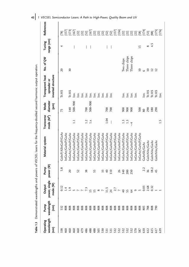
Table1.3
Dem
onstratedwavelen
gths
andpo
wersof
VEC
SELlasers
forthefrequency-do
ubledsecond
harm
onicou
tput
operation.
Operatin
gwavelength
(nm)
Pump
wavelength
(nm)
Outpu
tpo
wer,single
mod
e(W
)
Pump
power
(W)
Materialsystem
Tran
sverse
mod
e(M
2 )Mod
ediam
eter
(mm)
Transparentheat
spreader
orinverted
structure
No.
ofQW
Tuning
rang
e(nm)
References
338
532
0.12
5.8
GaInP/AlInGaP/G
aAs
75Tr.H
S20
4[78]
460
808
1.4
InGaA
s/GaA
sP/G
aAs
[157]
460
808
1.9
20InGaA
s/GaA
sP/G
aAs
140
Tr.H
S30
[173]
460
808
5InGaA
s/GaA
sP/G
aAs
1.1
500–90
0Inv.
—[167]
460
808
752
InGaA
s/GaA
sP/G
aAs
Inv.
[22]
479
808
7InGaA
s/GaA
sP/G
aAs
Inv.
[22]
486
808
7.3
38InGaA
s/GaA
sP/G
aAs
1.2
700
Inv.
—[52]
488
808
15InGaA
s/GaA
sP/G
aAs
1.x
500–90
0Inv.
—[167]
488
808
1555
InGaA
s/GaA
sP/G
aAs
Inv.
[22]
505
808
8InGaA
s/GaA
sP/G
aAs
Inv.
[22]
530
808
733
InGaA
s/GaA
sP/G
aAs
Inv.
[22]
531
808
11.5
40InGaA
s/GaA
sP/G
aAs
1.04
700
Inv.
—[52]
531
808
2411
0InGaA
s/GaA
sP/G
aAs
—70
0Inv.
—[52]
532
808
2.7
InGaA
s/GaA
sP/G
aAs
[157]
532
808
726
InGaA
s/GaA
sP/G
aAs
[156]
532
808
4014
0InGaA
s/GaA
sP/G
aAs
1.3
900
Inv.
Twochips
[22]
532
808
5520
0InGaA
s/GaA
sP/G
aAs
1.3
900
Inv.
Threechips
[22]
532
808
6425
0InGaA
s/GaA
sP/G
aAs
�490
0Inv.
Threechips
[22]
570
808
9InGaA
s/GaA
sP/G
aAs
Inv.
[22]
587
808
5InGaA
s/GaA
sP/G
aAs
500
1015
[58]
610
805
0.03
2.2
GaA
sSb/GaA
s80
Inv.
6[174]
612
788
2.68
36GaInNAs/GaA
s290
Tr.H
S10
8[53]
615
808
0.32
18.2
GaInNAs/GaA
s180
Tr.H
S12
4.5
[88]
617
790
145
GaInNAs/GaA
s290
Tr.H
S12
[175]
639
11.5
Inv.
[176]
42j 1 VECSEL Semiconductor Lasers: A Path to High-Power, Quality Beam and UV

output, have produced emission from 244nm in the deep UV to the 1180 nm in theNIR, a span of more than two octaves, with output powers from a few milliwattsto 64W.
As a side note, conventional intracavity frequency-doubled solid-state lasers aresusceptible to the so-called �green problem� [179], where lasers exhibit strongintensity noise due to nonlinear interactions between multiple modes of the laser.Intracavity frequency-doubledOPSL lasers do not suffer from the green problem [54]because of the short carrier lifetime in semiconductors and the resonant periodicgain structure of OPSLs that does not allow spatial hole burning. Thus, intracavityfrequency-doubled OPSLs have stable, low-noise output, so important for themajority of applications.
Still using GaAs substrates, the unstrained GaAlAs/GaAs material system ac-cesses directly the 850 nm wavelength region [55, 66, 120, 146], with powers as highas 1.6W [45, 47] demonstrated with in-well pumping. The same wavelength windowis accessed with barrier pumping by the strained InAlGaAs/InAlGaAsP/GaAsmaterial system using quaternary quantum wells and quinary strain compensatinglayers [86]. Still shorter wavelengths near 675 nm in the red are accessed directlyusing the InGaP/AlGaInP/GaAs material system [78, 79], demonstrating 1.1Woutput power. Such direct red-emitting VECSELs have also been pumped byGaN diode lasers [180]. Red-emitting VECSELs allow intracavity frequency doublinginto the UV wavelength regime, demonstrating 120mW output at 338 nmwavelength [78].
The shortest wavelength direct emission VECSEL demonstrated so far is theInGaN/AlGaN/GaN device that operated near 390 nm violet wavelength [95, 96]. Onedifficulty with such short-wavelength devices is finding a suitable simple pumpsource; in this case, the device was pumped by a frequency-tripledQ-switched pulsedoutput of a Nd:YAG laser [95].
Extending VECSEL wavelengths to the 1200–1350 nm NIR range has beenaccomplished using the GaInNAs/GaAs dilute nitride material system on GaAssubstrates [127]. Output powers as high as 1.4W at 1230 nm [88] and 0.6W at1322 nm [67] have been demonstrated; microchip mode of operation has also beenreported in thismaterial system [181].Watt-level emission has been demonstrated inthis material system at wavelengths as short as 1160–1210 nm [182]. Recently, usingAlGaInAs/InP material system and wafer fusion with GaAs-based mirror, outputpower of 2.7Whas been demonstrated at 1300 nmwavelengths [98]. Thiswavelengthregion is also important since it allows frequency doubling to the visible orange,590–620 nm, and red, 625–700 nm, wavelengths. Powers as high as 2.7W have beendemonstrated by this approach in the 612–617 nm orange–red wavelength re-gion [53, 88, 175]. Such doubled orange–red emission VECSEL has also beendemonstrated using the GaAsSb/GaAs material system [174]. In fact, the NIR rangeof such GaAs substrate VECSELs should be extendable all the way to the 1550 nmwavelength region using the GaInNAsSb/GaAs quinary material system [183].
The important 1500–1600 nm wavelength window for optical fiber communica-tion applications is covered by the InGaAsP/InP or InGaAlAs/InP material systemson InP substrates. Low refractive index contrast in thismaterial system leads to thick,
1.4 Demonstrated Performance of VECSELs and Future Directions j43

high thermal impedance laser mirrors; nevertheless, VECSEL output powers ashigh as 0.8W have been demonstrated [80, 121]. Using wafer fusion with GaAs-substrate-based mirrors, the InGaAlAs/InP active region has demonstrated stillhigher VECSEL powers of 2.6W [97, 98]. Electrically pumped VECSELs have alsobeen fabricated with 1550 nm emission wavelengths using InP-based materialsystem [92, 93, 152].
The 2000–2400 nm emission wavelength mid-IR region is covered by theGaInAsSb/GaSb material system. Output power as high as 5W has been demon-strated at 1980 nmusing standard 980 nmdiode pump [103]. More than 3Woutputhas been achieved at 2250 nmusing 980 nmdiode pumpwith a single-chip [81] anddual-chip [184] configurations, and at 2350 nmusing 1960 nm thulium-doped fiberlaser for in-well pumping [48, 185]. Even longer wavelength VECSELs withemission wavelength near 4.5 and 5 mm have been demonstrated using IV–VIlead–chalcogenide semiconductor material systems of PbTe (PbSe)/PbEuTe onboth BaF2 and Si substrates [82–85]. The long-wavelength VECSELs are discussedin more detail in Chapter 4.
Another approach to extend VECSEL emission to themid-IR and THzwavelengthregion is to use difference frequency generation [186], for example, with a dual-wavelength VECSEL [109–111]. Such nonlinear optical difference frequency gener-ation has been analyzed in Ref. [187], where dual emission VECSEL wavelengths at984 and 1042 nm are considered for 17.7 mm wavelength generation.
VECSEL lasers have also been used for generation of even longer wavelengthbroadband terahertz radiation in the 0.1–0.8THz frequency range [115], whichcorresponds to 0.4–3.0mmwavelength range. In this terahertz spectrometer arrange-ment, 480 fs pulses froma passivelymode-lockedVECSEL laser at 1044nmwere usedto illuminate both the emitter and the receiver photoconductive terahertz anten-nas [115].The accessible terahertz spectral range in this technique is givenby thebroadspectral bandwidth of the short pulses from a passively mode-locked VECSEL.
Broad gain bandwidth of semiconductor materials allows appreciable amount ofwavelength tuning from VECSELs, which has indeed been demonstrated inmany ofthe above material systems, as indicated in Tables 1.2 and 1.3. For example, 80 nmtuning range has been demonstrated near 1980 nmemissionwavelength in theGaSbmaterial system [103]. Even higher tuning range of 156 nm from 1924 to 2080 nm isreported in Ref. [188]. A tuning range of 33 nm has been demonstrated near 972 nmemission wavelength in a two-gain-chip VECSEL laser in the InGaAs/GaAsmaterialsystem [51]. Intracavity frequency-doubled VECSELs typically exhibit half the tuningrange at the second harmonicwavelength as the laser is capable of at the fundamentalwavelength. Thus, for example, frequency-doubled yellow laser at 587 nm wave-length exhibits 15 nm of tuning, as compared to the 30 nm tuning range at thefundamental 1174 nm wavelength [58].
To summarize, in the short time since VECSELs were first developed, theirdemonstrated wavelengths span from 244, 338, and 355 nm in the UV; to the violet,blue, green, yellow, orange, and red wavelengths in the visible 390–675 nm range; tothe 850–1570 nm NIR wavelength range; to the 2.0–2.35mm mid-IR range; to the
44j 1 VECSEL Semiconductor Lasers: A Path to High-Power, Quality Beam and UV

5mm further out in the mid-IR, and even out to terahertz radiation with 0.4–3.0mmwavelength range. What is important is that these wavelengths were targeted bydesign, often as required by specific application wavelength requirements. At someof these wavelengths, the materials for which had been subject of extensivedevelopment, power levels from watts to tens of watts had been demonstrated withexcellent beam quality. At other wavelengths with less-developed materials, powerlevels of tens and hundreds of milliwatts are more typical. This wavelength andpower flexibility of VECSELs, together with their beam quality and other advanta-geous properties, are key to the growing list of VECSEL applications, which we willdiscuss next.
1.4.2Commercial Applications
In their initial application,VECSEL laserswere developed as high-power single-modefiber-coupled sources at 980 nm for pumping Er-doped fiber and glass-waveguideamplifiers for optical fiber telecommunications systems [169, 189, 190]. Commercialoptically pumped OPSL lasers from Coherent Inc. and electrically pumped NECSELlasers from Novalux Inc. were targeting these potentially large telecom markets.Eventually, however, edge-emitting pump diode lasers came to dominate theseapplications. VECSEL lasers have been used in research for pumping other solid-state lasers, such as 2mm emitting Tm- and Ho-doped lasers pumped by a 1WGaInNAs/GaAs semiconductor disk laser at 1213 nm [182, 191, 192].
With the development of the intracavity frequency-doubled VECSEL laserswith emission wavelengths in the visible, the wavelength versatility of VECSEL,in combination with power scalability and beam quality, became key to theirmany successful commercial applications. Coherent Inc. pioneered the devel-opment and application of commercial OPSL lasers. Doubled into blue OPSLlasers with output at 460 and 488 nm became very successful solid-statereplacements for Ar-ion lasers in a wide range of fields. As compared to thebig, power inefficient, and limited lifetime Ar-ion lasers, blue OPSL lasers offercompact size, efficiency, low power consumption, beam pointing stability,excellent solid-state reliability with greater than 50 000 hours lifetime, and soon, thus bringing semiconductor laser advantages to visible wavelengths andpower levels not previously addressable by these lasers. The option of fiber-coupled delivery of the OPSL laser output is also important for many applica-tions. Relatively fast, 50 kHz–30MHz and higher, direct modulation capability ofOPSLs via pump current modulation is key to many applications, as it eliminatesthe need for separate acousto-optic modulators, required for the conventionaldiode-pumped solid-state DPSS lasers. One of the early applications of the OPSL460 nm blue laser from Coherent Inc. was in laser-based digital to film recordersfor transferring digitally produced or edited movies onto conventional 35mmcelluloid master film for cinema projection. ARRILASER film recorder from theARRI Group uses a blue OPSL laser, together with red and green laser sources,
1.4 Demonstrated Performance of VECSELs and Future Directions j45
and has been awarded a Scientific and Engineering Award, Oscar, in 2002 by theUS Academy of Motion Pictures Arts and Sciences.
With doubled into blue OPSL output powers scalable in the 10–200mW, theselasers found wide application in bioinstrumentation for confocal fluorescencemicroscopy [165, 166, 193–197], flow cytometry [198], optical trapping, and manip-ulation of cells [199], cell sorting, DNA sequencing, proteomics, drug discovery, andso on [16]. Inmost of these bioapplications, fluorescent marker dyes are used to labelfunctional molecules in the cells, and laser-excited fluorescence from these markerdyes is then detected or imaged. Alternatively, green fluorescent protein gene, and itsother fruit color variants [200], can be directly expressed in the cells ofmany differentorganisms, and the GFP fluorescence is then used tomonitor gene expression in thecells [16]. Specific wavelengths are required for optimal excitation of this imagingfluorescence [198, 200]; OPSL lasers have been designed with emission targetingthesewavelengths. The initial bluewavelengths of commercialOPSL lasers have laterbeen expanded to the green: 532 nm, yellow: 561 and 577 nm, red: 639 nm, andultraviolet: 355 nm emission. The availability of true CW UV emission from OPSLlasers is important for biological applications, where pulsed UV light from the moreconventional solid-state lasers can damage biological samples because of the highpeak powers of the pulsed lasers.
Coherent Inc. has also developed commercial high-power versions of OPSL laserswith CWoutput powers in the 0.5–8W range, with single- andmultitransversemodeemission, and, remarkably, with a laser head size as small as 12� 5� 7 cm3. Thiscombination of UV through visible wavelengths and a range output powers ad-dresses a variety of new applications. Multiwatt green output OPSLs have been usedto pump femtosecond mode-locked Ti:sapphire lasers [201]. Multiwatt green, blue,and yellow wavelength OPSL lasers have been used in a portable, battery-poweredlaser source for crime-scene fingerprint and trace evidence detection [22, 202]. Forthese applications, efficient battery-powered operation became possible becauseof the efficiency of the OPSL optical conversion of pump light and that the OPSLpump diodes do not require power-consuming tight wavelength/temperature sta-bilization of the kind required by the conventional diode-pumped solid-state lasers.Another application area for OPSL lasers is in entertainment, wheremultiwatt brightcolor blue, green, and yellow lasers with good beam quality are very effective for laserlight shows.
Multiwatt 532 nm green and 577 nm yellow OPSL lasers have been used inophthalmology for photocoagulation treatment of eye diseases, such as wet-formmacular degeneration and diabetic retinopathy [203]. The yellow 577 nmwavelengthis especially effective since it matches the absorption peak of the oxygenatedhemoglobin in blood. As a result of this wavelength matching, the OPSL laserdelivers effective treatment while less light is absorbed in the surrounding tissue.
Red, green, and blue lasers can be combined for RGB color projection dis-plays [204], ranging in size from full cinema projection [205] to laser television [206],to mobile micro projectors [207]. Laser projection displays can be made in threedifferent types [207]. The first type is a laser scanning or �flying spot� projector [208],where three primary color lasers are combined into a single beam and a mirror
46j 1 VECSEL Semiconductor Lasers: A Path to High-Power, Quality Beam and UV

system is used to scan this single-pixel beam in 2D over the imaging screensurface. The second type is a line scanning projector, where primary color lasersilluminate a linear array of pixels in a 1D spatial light modulator, such as gratinglight valve (GLV) [209], the resulting line image is then projected onto a screen andscanned by a mirror in 1D to produce a full image. The third type is an imagingprojector, where primary color lasers illuminate a 2D spatial light modulator pixelarray, such as Texas Instruments� digital micromirror digital light processor (DLP)chip, the resulting full image is then projected onto a screen. For example,Microvision�s mobile pico projector uses the first �flying spot� approach [207].Sony has been developing the second line scan approach for laser TV applicationsusing GLV technology [207]. The same GLV line scan approach is used by Evans &Sutherland in its ESLP�-8K laser projector [205]. Mitsubishi�s LaserVue� TV usesthe third 2D imaging approach. Such laser projection displays with saturatedprimary RGB colors can access a much wider color gamut [204] than is availablefrom other display technologies, such as liquid crystal and plasma displays.Different levels of laser power, from milliwatts to many watts, are required fordifferent size displays. Visible OPSL lasers can be used with all three types of laserdisplays and will play an important role here because of their power scaling,efficiency, beam quality, fast direct modulation capability, and access to the desiredemission wavelengths.
A number of companies have been working to develop OPSL/SDL/VECSELlasers for these display applications, such as Coherent, OSRAM, Samsung, andNovalux/Arasor. For mobile micro/pico projectors, such as the one developed byMicrovision Inc. using the �flying spot� laser scanning approach, direct emissionblue and red diode lasers are available; however, the green lasers are not availablebecause of the semiconductor material limitations. Doubled from NIR into green,several semiconductor laser approaches are being developed, including an exter-nally doubled diode laser from Corning and an intracavity frequency-doubled OPSLlaser from OSRAM Opto Semiconductors [207, 208]. OSRAM�s green OPSL laserfor mobile projectors emits 70mW at 530 nm, measures only 13� 6.5� 4.8mm3,and is capable of direct modulation at rates greater than 30MHz. Novalux/Arasorhas been developing NECSEL� electrically pumped VECSELs for display applica-tions [210], such as DLP-based LaserVue TV from Mitsubishi [206]; these lasers areamong the lasers used in the Evans & Sutherland ESLP-8K high-resolution 8K� 4Kdigital theater laser video projector [205].
Accessing a mid-IR 1.9–2.5mm wavelength range, Solus Technologies has devel-oped a 100mW narrow linewidth laser source for a range of applications from gassensing and molecular spectroscopy [106] to medical. Such lasers are potentiallycapable of watt-level operating powers, 100 nm wide tuning range, and single-frequency operation.
It is remarkable for this young technology that such a diversity of commercialOPSL lasers is available, with wavelengths from UV to mid-IR and output powersfrom milliwatts to watts, and that such a wide variety of applications is addressed,from bio-medical to forensics and to displays. This testifies to the flexibility andversatility of OPSL lasers that can successfully address all these varied application
1.4 Demonstrated Performance of VECSELs and Future Directions j47

requirements and where there is simply no other laser that can do the job aseffectively.
1.4.3Current and Future Research Directions
Future research directions and applications of VECSELs will surely reflect thealready demonstrated versatility of the VECSEL laser platform. Output powerscaling of VECSELs will continue to be a topic of interest. Power scaling canutilize a number of approaches, such as increasing mode area and pump spot sizewhile controlling and limiting the in-plane amplified spontaneous emission thatcan deplete the gain [159]. Further improvements in efficient heat removal(Chapter 2) will help, such as using the highest thermal conductivity diamondheat spreaders and heat sinks [107], front and back side heat removal from theOPS chip, design and fabrication of low thermal impedance semiconductorstructures, and so on. Further power scaling will be achieved by using multiplegain chips [22, 49, 50, 52, 184], with larger mode area per chip, from the currentmaximum �0.9mm diameter, and a larger number of OPS gain chips, from thepresently demonstrated maximum of three chips. Still further power scaling ispossible by spectrally combining multiple laser beams at different wavelengths, asdemonstrated by combining two VECSEL lasers preserving excellent beam qualityusing a volume Bragg grating [211]. VECSEL output powers of several hundredwatts, at the fundamental or the second harmonic, should be achievable withexcellent beam quality using some combination of the above techniques. Atthe same time, demonstrating compact and efficient, low-cost, manufacturableVECSELs with modest milliwatt- to watt-level output powers will also be impor-tant for many applications, such as mobile projection displays [207].
Wavelength scaling of VECSELs will likely proceed along two paths: one will beapplication-driven demonstrations of new wavelengths using the existing semi-conductormaterial systems and techniques; the otherwill explore newwavelengthsby using novelmaterial systems or novel nonlinear optical techniques to expand theversatility of the VECSEL approach. In addition to novel semiconductor materialsystems, finding suitable pump lasers and efficient pumping schemes for newVECSEL wavelength regions will also be important. For example, direct blueemission in the GaN material system [95, 96] with high powers and good beamswould be very useful; however, suitable pump diode lasers are not readily availableat the required wavelengths. Perhaps amultistage cascade of intracavity frequency-doubled VECSELs can be demonstrated, where output of one stage of such cascadeis used to pump the next stage of the cascade. A variety of nonlinear opticalfrequency conversion schemes should expand the range of accessible wavelengths:intracavity frequency doubling, tripling, and quadrupling; sum frequency gener-ation; difference frequency generation from dual wavelength lasers for accessingnew mid-IR wavelengths [109, 111], such as 17.7 mm [187]; a combination of laserintracavity and extracavity nonlinear conversions [77]; and using single and
48j 1 VECSEL Semiconductor Lasers: A Path to High-Power, Quality Beam and UV

multiple lasers for nonlinear optical conversions. VECSELs can become an im-portant compact source of broadband terahertz radiation by using ultrashort pulsemode-locked VECSELs in combination with photoconductive antennas [115]. Tosummarize, VECSELs wavelength coverage range will extend deeper into the UVand further intomid-IR, as well as start filling in the gaps in the existing wavelengthcoverage.
Tunable wavelength operation will prove important for many VECSEL applica-tions. The target herewill be to extend the relative wavelength tuning ranges from thecurrently demonstrated 3–8%, 33 nm tuning near 972 nm [51], 80 nm tuning near1980 nm [103], and 156 nm tuning near 2000 nm [188], to the 10–15% level. Thewaysto achieve this will include using broadband gain semiconductor materials, such asquantum dots (Chapter 5); broadband OPS chip gain structures with quantum well,or dot, layers displaced somewhat from their periodic RPG positions [18, 130];multiple, nonidentical gain chips in the cavity [51]; and, also important, low-losstunable filters. Single-frequency tuning of VECSELs [55, 140, 164] is also importantand will see further development for some applications, such as laser sources foratomic clocks [120, 146] and spectroscopy [106].
Development of new semiconductor materials both for gain and on-chip mirrorstructures will enable better performance of VECSELs and expand their operatingrange in terms of power, wavelength, tuning range, and so on. New semiconductormaterial systems with binary, ternary, quaternary, and quinary alloys can enableeasier materials growth with fewer defects for the gain region and better indexcontrast and lower thermal impedance for theVECSELmirrors.Unstrained or strain-compensated quantum well structures will be required in these material systems.Further development of the quantum dot active region (Chapter 5) [99–102] willenable VECSELs with reduced thresholds, wider gain bandwidth, and reducedtemperature dependence [101]. Bondingwafers of different semiconductormaterialsusing wafer fussion [97, 98], such as for bonding separate VECSEL mirror and gainwafers, eliminates some of the material limitations in VECSELs. Expanding the useof this technique will enable a range of novel better performing devices, for example,with higher powers and at new wavelengths. Wafer fusion of other VECSELfunctional blocks might also prove useful, such as bonding of gain regions atdifferent wavelengths, bonding of diode pump lasers to the gain region, and bondinggain and saturable absorbers for mode locking. New materials and epitaxial growthtechniques have been driving the development of semiconductor lasers for morethan 40 years, and they will also be critical for the future VECSEL development.Complexmultilayer semiconductor VECSEL structures require state-of-the-art semi-conductor materials and growth techniques. In addition, finding optimal nonlinearoptical materials, including periodically poled crystals, will boost performance of thefrequency-doubled visible emitting VECSELs.
Further development of electrically pumped VECSELs is an important topic offuture research. While optically pumped VECSELs will reach comparatively higheroutput powers, electrical pumping capability will enablemore compact, efficient, andsimple devices for many applications of VECSELs in a variety of operating regimes:
1.4 Demonstrated Performance of VECSELs and Future Directions j49

cw and pulsed, tunable, intracavity doubled, and so on. Electrically pumpedVECSELsare discussed in detail in Chapter 7.
Another important future direction for VECSEL research is the integration ofmultiple functional blocks on a common semiconductor substrate. For example,integration of pump lasers with the gain-mirror VECSEL structure has already beendemonstrated [154]. Further development of such pump-integrated VECSELs canproduce highly manufacturable high-power lasers that require significantly reducedcomponent assembly, thus reducing the device cost and expanding the potentialmarkets for these lasers. Another example of functional component integration isthe MIXSEL laser (Chapter 6) [160, 161], where gain and saturable absorber regionsof short-pulse mode-locked VECSELs are integrated on a common substrate. Animportant direction of functional integration is the development of various forms ofVECSEL-integrated optical cavities; such integrated cavities are more compact andbetter manufacturable and might prove very valuable for some applications. Thisincludes plane–plane microchip cavities with thermally stabilized transverse modes[69–71, 181]; compact plane–curved cavities where the curved surface is producedas a microlens on an optical substrate [141–144, 212, 213]; and single-transversemode optical resonators, for example, in the pillbox configuration [145]. Suchfunctional integration, including combinations of the above schemes, can producesimpler, more compact, easier manufacturable, and cheaper devices, as well asenable better device performance and novel functions. Future development offunctional integration can help make VECSELs even more widely used commer-cially, especially in low-cost and high-volume applications, such as mobile projec-tion displays.
A variety of optical cavity configurations have been used with VECSELs; develop-ment of optical cavities optimized for different applications will play an importantrole in expanding VECSEL function and application.While integrated optical cavitiesmentioned above are important, compact bulk optical cavities with large modearea for high-power operation [52] will also be valuable. Optical cavity design is animportant factor in VECSELs incorporatingmultipleOPS chips [22, 49–52, 135, 184].VECSELs using intracavity nonlinear optical crystals for harmonic generation orsaturable absorbers formode locking require optical cavities that control the absoluteand relative laser mode diameters in the gain and the nonlinear element. In contrastwith most VECSELs that use a linear laser cavity, even if with multiple cavityelements, ring laser cavity has been used in a VECSEL-based laser gyro [137] anda passively mode-locked VECSEL [136]. A diffractive unstable optical resonator hasbeen used with VECSELs where Gaussian beam output was extracted from a hard-edged outcoupling aperture [138]. VECSELs have also been operated in unstableresonator regime with plane–spherical resonator cavities [18]. Optimized and noveloptical cavities will enable VECSELs with enhanced performance, while makingthem more compact, stable, and manufacturable.
Array operation of VECSELs has been demonstrated both with electrical(Chapter 7) and optical [70, 143] pumping. This is a promising research directionfor producing higher output powers from multiple beam incoherent arrays(Chapter 7) or phase-locked arrays [214]. Individually addressable VECSEL arrays
50j 1 VECSEL Semiconductor Lasers: A Path to High-Power, Quality Beam and UV

can be used for optical micromanipulation applications, such as optical trapping andtransport of biological cells [215]. Incoherent arrays of VECSELs also producereduced laser speckle for illumination applications, such as in imaging projectiondisplays [210], where laser speckle reduces as the square root of the number of arrayelements.
VECSEL laser power modulation is important for many applications, such as forlaser projection displays. Laser power can be modulated directly by current forelectrically pumpedVECSELs [49] or via pumpdiode currentmodulation for opticallypumped VECSELs [207, 208]. Exploring modulation properties of VECSELs of bothtypes and optimizing their high-speed modulation performance is an importantfuture research direction. For example, pumping a VECSEL with multiple pumpdiodes connected in series can yield a high slope differential modulation capabilityuseful in microwave photonics applications. Fast laser wavelength tuning mightalso prove important; such fast tuning is possible with MEMS-tunable opticallypumped VECSELs that were developed for optical fiber communication applica-tions [216–218].
A range of VECSEL applications require single-frequency laser operation, bothtunable and nontunable, for example, molecular spectroscopy [106, 219], pumpingof atomic clocks [120, 146], ring laser gyro [137], and microwave photonics applica-tions [56, 220]. A number of studies have explored properties of VECSELs in theirsingle-mode operating regime, such as laser linewidth, which can be very narrow inthe kilohertz range [55, 104, 106, 119], and relative intensity noise (RIN) and itsspectrum [56, 140]. Such single-mode operation has been achieved both withintracavity filters [55, 56, 59, 221], such as etalons, birefringent filters, and volumeBragg gratings, or alternatively free running without intracavity filters [106, 140].Single-mode operation has been demonstrated both for the fundamental andintracavity frequency-doubled VECSELs [222]. Further investigation of the single-mode VECSEL regime and understanding of its properties can yield devices withunique characteristics for the above-mentioned applications, such as hertz-levelquantum-limited linewidth [119] and shot-noise limited RIN [56], while at the sametime with watt-level output powers and potentially tunable over several tens ofnanometers wavelength range.
Short pulses at gigahertz repetition rates have been generated by saturableabsorber passive mode locking of VECSELs [20]; this topic is discussed in detailin Chapter 6. Such passive mode locking has been demonstrated with both optical-ly [62, 134, 223–226] and electrically [227–230] pumped VECSELs. Some of theremarkable characteristics demonstrated with passively mode-locked VECSELs aretransform-limited pulses as short as 220 fs [231], repetition rates as high as50GHz [62], timing jitter as low as 160 fs with actively stabilized laser [232], andaverage output powers as high as 2.1W [133], all with excellent circular output beams.Saturable absorbers have also been integrated with the gain medium on the samesemiconductor substrate for a very simple and compact implementation of apassively mode-locked VECSEL or MIXSEL [160, 161]. Alternatively to saturableabsorber passive mode locking, VECSELs have also been actively mode-locked bysynchronous pumping with picosecond and femtosecond pulses from a Ti:sapphire
1.4 Demonstrated Performance of VECSELs and Future Directions j51

laser [233]. The resulting chirped picosecond pulses were compressed down to 185 fsby a grating pair compressor. Semiconductor gain medium, unlike traditional solid-state laser materials, for example, Yb:YAG, does not have long storage times;therefore, high pulse energy regime is outside the scope of VECSEL characteristics.VECSEL sources of high-power ultrashort pulses at gigahertz repetition rates willfind applications in such areas as optical clock distribution in high-speed computingsystems and metrology. Future research will expand the short pulse generationperformance of VECSELs in the direction of shorter femtosecond pulses, higherrepetition rates beyond 100GHz, new operating wavelengths from UV to mid-IRwith different material systems and nonlinearly converted optical frequencies,compact integrated implementations, and further development of electricallypumped devices. Such compact high-power ultrashort pulse sources will findmany applications and will displace more conventional solid-state pulsed sourcesin many application areas.
Microwave photonics applications transmit analogue radio frequency (RF) ormicrowave signals modulated on top of an optical carrier. VECSELs are exceptionallysuited as light sources for suchmicrowave links because of their high power and shot-noise-limited RIN capability [56]. With a high-Q external cavity, VECSELs operate inthe flat-noise oscillation-relaxation-free class-A laser regime, achieved becausephoton lifetime in the VECSEL laser cavity is much larger than the carrier lifetimein the gain chip [119, 220]. Application of VECSELs to microwave photonics links isa promising direction of future development.
With their high-power, tunable, single-mode, and narrow-linewidth operationcapability, VECSELs are a good laser light source for pumping atomic clocks, such asCs atomic clock near 852 nm [120, 146]. Here, VECSELs can be used for trapping,cooling,manipulation, and optical detection of atoms. Theuse ofVECSELs for opticaltweezers for trapping and manipulation of biological samples [199] is also an area offuture research interest; output power, wavelength, and beam quality, all in compactsize, are key VECSEL qualities for these applications.
Another interesting application of VECSELs is for rotation sensing usingVECSEL-based ring laser gyro [137]; the initial demonstration of such laser gyrosis certain to be followed by many others. High power, excellent beam quality, andwavelength selection of VECSELs have a natural application for a sodium laserguide star [58, 234]. Here amultiwatt 589 nm yellow laser beam is used to excite theD2 sodium line in the mesospheric layer of sodium atoms, creating a glowingartificial �star� in the regions of the sky where no bright stars are available. Thissodium guide star is then used for adaptive optics compensation of atmosphericdistortion in ground-based astronomical telescopes [234, 235] and in space–groundoptical links.
Important for the future development and broad application of VECSELs isdetailed physical modeling, including analytical and numerical models, of variousaspects of their behavior. One example that is already bearing fruit is the modelingof the thermal heat dissipation issues in VECSELs [20, 72, 236, 237]; this subject isdiscussed in detail in Chapter 2. Modeling and understanding of the short pulse
52j 1 VECSEL Semiconductor Lasers: A Path to High-Power, Quality Beam and UV

generation mechanisms in VECSELs, including cavity group delay dispersion(GDD), nonlinear self-phase modulation (SPM), and gain and loss saturationdynamics, has enabled decreasing mode-locked pulse widths from the picosecondto the femtosecond regime [20, 134, 238], with further pulse width decreasesexpected in the future. Modeling of the VECSEL single-mode regime nonlineardynamics and noise [119, 239] will produce higher performing devices formicrowave photonics and atomic clock applications. Further application of fullnumerical microscopic models of semiconductor lasers, including gain propertiesof semiconductor materials [117, 118], as well as modeling of gain and carrierbehavior in VECSELs [240, 241], will lead to better understanding of the laserbehavior and design of improved performance lasers. Detailed modeling is alsorequired for improving the performance of electrically pumped VECSELs(Chapter 7).
An important application area of VECSELs of much research is in molecularspectroscopy. Tunable single-frequency VECSELs have been used directly to acquirespectra in the NIR by scanning the laser line across absorption features of interest,for example,methane absorption near 2.3mm [106, 219, 242]. Detection sensitivity ofVECSEL spectroscopy can be magnified with cavity-enhanced absorption spectros-copy [243], where amode-locked VECSEL frequency comb ismatched to the comb ofresonances of a high-finesse cavity containing gas under study. Using this technique,acetylene absorption near 1mmwas measured with a 25m effective absorption pathlength for a 13 cm long cell [243].
Even greater enhancement of detection sensitivity in molecular spectroscopy isobtained with an ultrasensitive ICLAS technique, first demonstrated with VECSELsinRefs [73, 74]. In this technique, the absorption cell is placed inside optical cavity of ahomogeneously broadened multimode laser, the laser is turned on, and the lasingspectrum ismeasured by a spectrometer a time tg later within a narrow time slotDtg.This approach gives effective absorption path length Lp ¼ rctg, where r is the lengthfraction of the laser occupied by the absorption cell and c is the speed of light. For thetypical generation times of 200–400ms and a 50 cm long absorption cell, the effectiveabsorption path lengths are 30–60 km; effective path lengths as long as 130 kmhave been demonstrated for a 1m long absorbing path [244]. Due to the long effectivepath lengths, ICLAS-VECSEL allows measurement of absorption coefficients as lowas 10�9–10�10 cm�1 (sensitivity �10�11 cm�1Hz�1/2). Acousto-optic modulator isused to switch the laser beam to the measuring spectrometer; both grating andFourier transform spectrometers have been used for spectrum acquisition in ICLAS.Several properties of VECSELs enable their application to ICLAS: wide range ofavailable wavelengths, broad homogeneous gain bandwidth, and very low loss lasercavity; because of their high loss, edge-emitting semiconductor lasers are not verysuitable for ICLAS. ICLAS-VECSEL technique has been applied for molecularspectroscopy measurements at wavelengths near 1.0mm (8900–10 100 cm�1)[74, 244, 245], 1.55mm (6500 cm�1) [148], and 2.3 mm (4300 cm�1) [246]. Withits high sensitivity, ICLAS-VECSEL can be used for trace gas detection or formeasurement of weak absorption lines of atmospheric gases. A variety of molecular
1.4 Demonstrated Performance of VECSELs and Future Directions j53

gases have beenmeasured by ICLAS-VECSEL, detecting thousands of spectral lines,including new ones. Rovibrational analysis has been used to assign the detectedlines [247]. Some of the measured molecular species are nitrous oxide (N2O) [245],water (H2O) [148, 244, 246–248], carbon dioxide (CO2) [148, 246], hydrogen sulfide(H2S) [249], acetylene (HCCH) [248], and carbonyl sulfide (OCS) [250], as well as avariety of isotopic variants such as D2O [251]. Prior to the development of semicon-ductor VECSELs, ICLAS relied primarily on Ti:sapphire laser in the 700–900 nmrange and dye lasers in the visible range. Semiconductor VECSELs opened newwavelengths for ICLAS in the NIR and mid-IR 0.9–2.5mm wavelength,4000–11 000 cm�1 wave number, including the spectrally rich molecular overtoneregion. VECSELs also offer a simple and compact laser source for spectroscopy.Using VECSELs for ICLAS revealed an unexpected spectral condensation effect,where spectral absorption dips are replaced by blue-shifted emission peaks at longergeneration times [248]. ICLAS-VECSEL promises to be an active research area inthe future with more molecular species observed, improved detection sensitivities,and expanded spectral detection regions in the NIR and mid-IR. Highly sensitiveICLAS-VECSEL gas detection canhave applications in understanding of atmosphericgases and in medicine.
To summarize this section, current research work has explored an amazing varietyof applications that exploit the unique properties of VECSELs. Further research intoexpanding, improving, andunderstanding of theVECSEL properties will lead to evengreater growth in the future of the research and commercial applications of theseremarkable lasers.
1.4.4Future of VECSEL Lasers: Scalable Power with Beam Quality from UV to IR
This chapter has outlined a new semiconductor laser technology that comes withseveral alternative names: vertical-external-cavity surface-emitting laser, semicon-ductor disk laser, or optically pumped semiconductor laser. This is one technologythat, uniquely among various other laser technologies, addresses simultaneouslymultiple laser application requirements: power scaling, wavelength versatility,beam quality, compact size, efficiency, reliability, and so on. This technology allowslaser design with characteristics to match application requirements optimally, forexample, output power from milliwatts to tens of watts, wavelength from UV tomid-IR, and an excellent beam quality. It should be emphasized that VECSELtechnology achieves the desired laser characteristics by design, rather than byhoping for a serendipitous coincidence, as with solid-state and gas laser wavelengthtargeting.
What is the source of these remarkable properties of VECSEL technology? Theanswer is, as this chapter has described, that VECSELs combine some of the bestqualities of semiconductor lasers and solid-state lasers, while avoiding many of theweaknesses of these two laser classes.
What are VECSEL strengths acquired from semiconductor lasers? VECSELs takefrom semiconductor lasers the use of semiconductor materials with their various
54j 1 VECSEL Semiconductor Lasers: A Path to High-Power, Quality Beam and UV

binary compounds and multicomponent alloys that can target a very wide range ofemission wavelengths. VECSELs have also incorporated bandgap-engineered semi-conductor heterostructures that are used to engineer by design the desired laseremission and pumpabsorption properties.Due to the semiconductor lasermaterials,optically pumped VECSELs have strong pump absorption in a very thin layer, just afew microns thick, and over extremely wide range of pump wavelengths, tens andhundreds of nanometers. VECSELs have also inherited the excellent circular outputbeam of a VCSEL surface-emitting semiconductor laser.
What are VECSEL strengths acquired from the solid-state lasers? The key contri-bution of solid-state lasers to VECSELs is the flexible optical laser cavity, whichenablesmany of the key VECSEL properties. Optical cavity provides transversemodecontrol to VECSELs, which enables their excellent beam quality. VECSEL opticalcavity also enablesmode size scaling for laser output power scaling.More important,flexible open laser cavity makes possible for VECSELs the insertion of variousintracavity functional optical elements, such as nonlinear optical crystals for har-monic generation, saturable absorbers for short pulse passivemode locking,multiplegain chips, optical filters for spectral control, and so on. This gives VECSELs manydifferent regimes of operation and underlies their tremendous functional flexibility.Significantly, both solid-state laser and VECSEL optical cavity has low intracavity loss.This has important consequences by allowing efficient use of low transmissionoutput coupling, which in turn results in high intracavity power compared to outputlaser power and thus enables very high nonlinear optical conversion efficiency.Another feature acquired by VECSELs from solid-state lasers is optical pumping.While electrical pumping of VECSELs is preferred in some cases, optical pumpingproduces much higher VECSEL output powers and allows much simpler VECSELlaser wafer structure.
Many VECSEL properties are enabled by avoiding some of the key weaknesses ofsemiconductor lasers. Edge-emitting semiconductor lasers have their light locked ina waveguide; good beam quality requires this to be a single-mode waveguide, whichresults in a nonscalable small lasermode size that limits laser output powerwith goodbeam quality. Surface-emitting VCSEL lasers have no adequate transverse modecontrol and good beam quality single-transversemode output power is again limited.In contrast, VECSELs avoid these limitations; they have open cavities, allowing bothtransverse mode control for fundamental circular mode operation and mode sizescaling for higher output powers. Another disadvantage of edge-emitting semicon-ductor lasers is their lossy optical cavity, both due to lossy waveguides, which giveloss of several tens of percent per cavity pass, and due to lossy coupling to externaloptical cavity. Lossy cavities of edge-emitting lasers require for output powerefficiency the use of high-transmission output couplers, hence intracavity powerbecomes comparable to output power, and thus no efficient intracavity-enhancednonlinear optical frequency doubling is possible. Lossy cavity also produces strongspontaneous emission noise. In contrast, VECSELs with their low-loss laser cavitiesdo not have these limitations.
What are the weaknesses of solid-state lasers avoided by VECSELs? The keyweakness of solid-state lasers is very inflexible emission wavelengths, which are
1.4 Demonstrated Performance of VECSELs and Future Directions j55

constrained to the few available transitions of active ions. The second weakness, forsimilar reasons, is the very inflexible narrow range of pump wavelengths; pumpdiode lasers at such wavelengths might not be readily available, when available, theyrequire costly wavelength stabilization, for example, by temperature stabilization.Another limitation of solid-state lasers is relatively weak, compared to semiconduc-tors, pump absorption, thus requiring thicker crystals for efficient pump absorption.Thicker absorbing crystals require complex pump optics and relatively good qualitypump beams; thicker crystals also produce thermal lensing, which distorts beamand limits output power. VECSELs avoid these limitations due to strong broadbandpump absorption of semiconductors.
The solid-state lasers typically have fairly long excited-state lifetimes, which can beas long as amillisecond, allowing energy storage and high-energy pulse generation inthese lasers. On the other hand, the long carrier lifetime of solid-state lasers severelylimits their output modulation rate and typically requires external modulation.In contrast, semiconductor materials of VECSEL have very short carrier lifetimesof the order of a nanosecond. As a result, VECSELs lose the energy storage and thehigh pulse energy capabilities of solid-state lasers. However, due to the short carrierlifetime, VECSELs acquire fast modulation capability, either directly via currentmodulation for electrically pumped VECSELs or via pump diode power modulationfor optically pumped VECSELs.
This combination of advantageous laser properties in VECSELs produces a veryflexible and versatile laser technology, as illustrated by the multitude of researchdirections described above: power scaling frommilliwatts to tens of watts with singleor multiple gain chips, UV and visible output wavelengths via harmonic generation,wavelength tunable operation, femtosecond short pulse generation at gigahertz highrates, single-frequency operation, intracavity laser absorption spectroscopy, lasergyros, microwave photonics, terahertz spectroscopy, and so on. Versatile VECSELlaser technology leads to an impressive and surprising variety of commercialapplications already demonstrated for this new technology: from biomedical fluo-rescence imaging to ophthalmic photocoagulation treatment, to projection displays,to forensic evidence analysis, to pumping Ti:sapphire lasers. VECSEL applications sofar have beenmostly in the UVand visible wavelengths, where compact and efficientsources with other laser technologies have been lacking. The accomplishments untilnow for the young VECSEL laser technology only illustrate its rich potentials; futureresearch and development are going to expand even wider the scope of VECSELperformance, functional versatility, and the range of scientific and commercialapplications.
What is the future of VECSEL lasers? VECSELs will expand the range of theircapabilities both through technology push and amarket pull. VECSEL technologywillexpand the range of VECSEL-operating parameters: output powers will increase tothe hundreds ofwatts levelsmaintaining excellent beamquality; wavelength coveragewill expand deeper into UV below 200nm and further intomid-IR beyond 5mmwithmore complete wavelength coverage inside this range; shorter pulses in the tens offemtoseconds will become possible, with increased average power levels of multiplewatts; single-frequency operation with subkilohertz linewidth will be demonstrated;
56j 1 VECSEL Semiconductor Lasers: A Path to High-Power, Quality Beam and UV

and VECSELs will become efficient sources of terahertz radiation. At the same time,various VECSEL performance parameters will be optimized: expect higher powerefficiencies; smaller laser packages; further integration of various functional com-ponents, such as pump lasers, saturable absorbers, and optical cavities; and electricalpumping will be usedmore widely when needed and possible. VECSELs will be usedmore widely in novel scientific applications, such as molecular spectroscopy withICLAS, laser gyros, microwave photonics, and atomic clocks. Market pull fromexisting and developing applications will stimulate appearance of new commercialdevices, for example,multiwatt red, green, and blue (RGB)VECSEL lasers for cinemaprojection applications. The availability of compact, efficient, and high-performancelasers with targeted custom-designed wavelength and other parameters will expandtheir use in existing commercial applications and will enable new applications thatcould not be addressed previously with other laser technologies. VECSELs will bedisplacing other laser technologies in some applications areas, for example, Ar-iongas lasers with the blue and green wavelength outputs have been used in the past asthe only suitable source for confocal fluorescence microscopy and for pumping Ti:sapphire lasers. These gas lasers have largely been displaced by diode-pumped solid-state lasers at these wavelengths; solid-state lasers in turn are in the process of beingthemselves displaced by VECSELs in these application areas. For these applications,VECSELs offer wavelength flexibility, power scalability, beam quality, compact size,good efficiency, and high reliability.
We are entering a new era of VECSEL/SDL/OPSL lasers that are poised to becomeubiquitous laser sources in scientific and commercial applications. Perhaps some ofthe more interesting future VECSEL developments are the unexpected ones; futureof VECSELs will be full of bright surprises.
Acknowledgments
I would like to acknowledge my former colleagues at Micracor Inc. who greatlycontributed to the development of the first VECSEL lasers: AramMooradian, FarhadHakimi, and Robert Sprague. I am also grateful to Oleg Okhotnikov for putting thisbook collection together.
References
1 Svelto, O. (1998) Principles of Lasers,4th edn, Springer.
2 Agarwal, G.P. (2002) Fiber-OpticCommunication Systems, 3rd edn,Wiley–Interscience.
3 Agrawal, G.P. and Dutta, N.K. (1986)Long-Wavelength Semiconductor Lasers,Van Nostrand Reinhold Co., New York.
4 Zory, P.S. (ed.) (1993) Quantum WellLasers, Academic Press, San Diego.
5 Chuang, S.L. (1995) Physics ofOptoelectronic Devices, JohnWiley & Sons,Inc., New York.
6 Coldren, L.A. and Corzine, S.W. (1995)Diode Lasers and Photonic IntegratedCircuits, John Wiley & Sons, Inc.,New York.
7 Chow, W. and Koch, S.W. (1999)Semiconductor Laser Fundamentals,Springer, Berlin.
References j57

8 Kapon, E. (ed.) (1999) SemiconductorLasers I: Fundamentals, AcademicPress.
9 Kapon, E. (ed.) (1999) SemiconductorLasers II: Materials and Structures,Academic Press.
10 Wilmsen, C.W., Temkin, H., andColdren, L.A. (eds) (1999) Vertical-CavitySurface-Emitting Lasers: Design,Fabrication, Characterization, andApplications, Cambridge UniversityPress.
11 Li, H. and Iga, K. (eds) (2002) Vertical-Cavity Surface-Emitting Laser Devices,Springer.
12 Diehl, R. (ed.) (2000) High Power DiodeLasers, Springer.
13 Koechner, W. (2006) Solid-State LaserEngineering, 6th edn, Springer.
14 Koechner, W. and Bass, M. (2003)Solid-State Lasers: A Graduate Text,Springer.
15 Digonnet, M.J.F. (ed.) (2001) Rare-Earth-Doped Fiber Lasers and Amplifiers,2nd edn, CRC Press.
16 Prasad, P.N. (2003) Introduction toBiophotonics, Wiley-Interscience.
17 Kuznetsov, M., Hakimi, F., Sprague, R.,and Mooradian, A. (1997) High-power(>0.5-W CW) diode-pumped vertical-external-cavity surface-emittingsemiconductor lasers with circularTEM00 beams. IEEE Photon. Technol.Lett., 9, 1063–1065.
18 Kuznetsov, M., Hakimi, F., Sprague, R.,and Mooradian, A. (1999) Design andcharacteristics of high-power(>0.5-W CW) diode-pumped vertical-external-cavity surface-emittingsemiconductor lasers with circularTEM00 beams. IEEE J. Sel. Top. QuantumElectron., 5, 561–573.
19 Tropper, A.C., Foreman,H.D., Garnache,A., Wilcox, K.G., and Hoogland, S.H.(2004) Vertical-external-cavitysemiconductor lasers. J. Phys. D: Appl.Phys., 37, R75–R85.
20 Keller, U. and Tropper, A.C. (2006)Passively modelocked surface-emittingsemiconductor lasers. Phys. Rep., 429,67–120.
21 Tropper, A.C. and Hoogland, S. (2006)Extended cavity surface-emitting
semiconductor lasers. Prog. QuantumElectron., 30, 1–43.
22 Chilla, J., Shu, Q.-Z., Zhou,H.,Weiss, E.,Reed, M., and Spinelli, L. (2007) Recentadvances in optically pumpedsemiconductor lasers. Proc. SPIE, 6451,645109.
23 Schulz, N., Hopkins, J.M., Rattunde, M.,Burns, D., and Wagner, J. (2008) High-brightness long-wavelengthsemiconductor disk lasers. Laser Photon.Rev., 2, 160–181.
24 Calvez, S., Hastie, J.E., Guina, M.,Okhotnikov, O.G., and Dawson, M.D.(2009) Semiconductor disk lasers for thegeneration of visible and ultravioletradiation. Laser Photon. Rev., 3 (5),407–434.
25 Boyd, R.W. (2008) Nonlinear Optics,3rd edn, Academic Press.
26 Seurin, J.-F., Xu, G., Khalfin, V.,Miglo, A., Wynn, J.D., Pradhan, P.,Ghosh, C.L., and D�Asaro, L.A. (2009)Progress in high-power high-efficiencyVCSEL arrays. Proc. SPIE, 7229,722903–722911.
27 Delfyett, P.J., Shi, H., Gee, S., Barty,C.P.J., Alphones, G., and Connolly, J.(1998) Intracavity spectral shaping inexternal cavity mode-lockedsemiconductor diode lasers. IEEE J. Sel.Top. Quantum Electron., 4, 216–223.
28 Hadley, M.A., Wilson, G.C., Lau, K.Y.,and Smith, J.S. (1993) High single-transverse-mode output from external-cavity surface-emitting laser diodes.Appl.Phys. Lett., 63, 1607–1609.
29 Chinn, S.R., Rossi, J.A., Wolfe, C.M., andMooradian, A. (1973) Optically pumpedroom-temperature GaAs lasers. IEEE J.Quantum Electron., QE-9, 294–300.
30 Stone, J., Wiesenfeld, J.M., Dentai, A.G.,Damen, T.C., Duguay, M.A., Chang, T.Y.,and Caridi, E.A. (1981) Optically pumpedultrashort cavity In1 �xGaxAsyP1�y lasers:picosecond operation between 0.83 and1.59 mm. Opt. Lett., 6, 534–536.
31 Roxlo, C.B. and Salour, M.M. (1981)Synchronously pumped mode-lockedCdS platelet laser. Appl. Phys. Lett., 38,738–740.
32 Le, H.Q., Di Cecca, S., andMooradian, A.(1991) Scalable high-power optically
58j 1 VECSEL Semiconductor Lasers: A Path to High-Power, Quality Beam and UV

pumped GaAs laser. Appl. Phys. Lett., 58,1967–1969.
33 McDaniel, D.L., Jr., McInerney, J.G.,Raja, M.Y.A., Schaus, C.F., and Brueck,S.R.J. (1990) Vertical cavity surface-emitting semiconductor laser with cwinjection laser pumping. IEEE Photon.Technol. Lett., 2, 156–158.
34 Sandusky, J.V. and Brueck, S.R.J. (1996)A CW external-cavity surface-emittinglaser. IEEE Photon. Technol. Lett., 8,313–315.
35 Hanaizumi, O., Jeong, K.T., Kashiwada,S.-Y., Syuaib, I., Kawase, K., andKawakami, S. (1996) Observation of gainin an optically pumped surface-normalmutiple-quantum-well optical amplifier.Opt. Lett., 21, 269–271.
36 Jiang, W.B., Friberg, S.R., Iwamura, H.,and Yamamoto, Y. (1991) High powersand subpicosecond pulses from anexternal-cavity surface-emitting InGaAs/InP multiple quantum well laser. Appl.Phys. Lett., 58, 807–809.
37 Sun, D.C., Friberg, S.R., Watanabe, K.,Machida, S., Horikoshi, Y., andYamamoto, Y. (1992) High power andhigh efficiency vertical cavity surfaceemitting GaAs laser. Appl. Phys. Lett., 61,1502–1503.
38 Le, H.Q., Goodhue, W.D., and Di Cecca,S. (1992) High-brightness diode-laser-pumped semiconductor heterostructurelasers. Appl. Phys. Lett., 60, 1280–1282.
39 Le,H.Q.,Goodhue,W.D.,Maki, P.A., andDi Cecca, S. (1993) Diode-laser-pumpedInGaAs/GaAs/AlGaAs heterostructurelasers with low internal loss and 4-Waverage power. Appl. Phys. Lett., 63,1465–1467.
40 Stewen, C., Contag, K., Larionov, M.,Giesen, A., and Hugel, H. (2000) A 1-kWCW thin disc laser. IEEE J. Sel. Top.Quantum Electron., 6, 650–657.
41 Giesen, A. and Speiser, J. (2007) Fifteenyears of work on thin-disk lasers: resultsand scaling laws. IEEE J. Sel. Top.Quantum Electron., 13, 598–609.
42 Corzine, S.W., Geels, R.S., Scott, J.W.,Yan, R.-H., and Coldren, L.A. (1989)Design of Fabry–Perot surface-emittinglaserswith a periodic gain structure. IEEEJ. Quantum Electron., QE-25, 1513–1524.
43 Lutgen, S., Albrecht, T., Brick, P., Reill,W., Luft, J., and Spath, W. (2003) 8-Whigh-efficiency continuous-wavesemiconductor disk laser at 1000 nm.Appl. Phys. Lett., 82, 3620–3622.
44 Schmid, M., Benchabane, S., Torabi-Goudarzi, F., Abram, R., Ferguson, A.I.,and Riis, E. (2004) Optical in-wellpumping of a vertical-external-cavitysurface-emitting laser. Appl. Phys. Lett.,84, 4860–4862.
45 Zhang, W., Ackemann, T., McGinily, S.,Schmid, M., Riis, E., and Ferguson, A.I.(2006) Operation of an optical in-well-pumped vertical-external-cavity surface-emitting laser. Appl. Opt., 45, 7729–7735.
46 Beyertt, S.S., Zorn, M., Kubler, T.,Wenzel, H., Weyers, M., Giesen, A.,Trankle, G., and Brauch, U. (2005)Optical in-well pumping of asemiconductor disk laser with highoptical efficiency. IEEE J. QuantumElectron., 41, 1439–1449.
47 Beyertt, S.S., Brauch, U., Demaria, F.,Dhidah, N., Giesen, A., Kubler, T., Lorch,S., Rinaldi, F., and Unger, P. (2007)Efficient gallium–arsenide disk laser.IEEE J. Quantum Electron., 43, 869–875.
48 Schulz, N., Rattunde, M., Ritzenthaler,C., Rosener, B., Manz, C., Kohler, K., andWagner, J. (2007)Resonant optical in-wellpumping of an (AlGaIn)(AsSb)-basedvertical-external-cavity surface-emittinglaser emitting at 2.35 mm. Appl. Phys.Lett., 91, 091113.
49 Saarinen, E.J., Harkonen, A.,Suomalainen, S., and Okhotnikov, O.G.(2006) Power scalable semiconductordisk laser usingmultiple gain cavity.Opt.Express, 14, 12868–12871.
50 Fan, L., Fallahi, M., Hader, J., Zakharian,A.R.,Moloney, J.V., Murray, J.T., Bedford,R., Stolz, W., and Koch, S.W. (2006)Multichip vertical-external-cavity surface-emitting lasers: a coherent power scalingscheme. Opt. Lett., 31, 3612–3614.
51 Fan, L., Fallahi, M., Zakharian, A., Hader,J.,Moloney, J.V., Bedford, R.,Murray, J.T.,Stolz,W., andKoch, S.W. (2007) Extendedtunability in a two-chip VECSEL. IEEEPhoton. Technol. Lett., 19, 544–546.
52 Hunziker, L.E., Ihli, C., and Steingrube,D.S. (2007) Miniaturization and power
References j59

scaling of fundamental mode opticallypumped semiconductor lasers. IEEE J.Sel. Top. Quantum Electron., 13,610–618.
53 Rautiainen, J., Harkanen, A., Korpijarvi,V.M., Tuomisto, P., Guina, M., andOkhotnikov, O.G. (2007) 2.7 W tunableorange–red GaInNAs semiconductordisk laser.Opt. Express, 15, 18345–18350.
54 Seelert,W., Butterworth, S., Rosperich, J.,Walter, C., Elm, R.v., Ostroumov, V.,Chilla, J., Zhou, H., Weiss, E., andCaprara, A. (2005) Optically pumpedsemiconductor lasers: a new reliabletechnique for realizing highly efficientvisible lasers. Proc. SPIE, 5707, 33–37.
55 Holm, M.A., Ferguson, D., and Dawson,M.D. (1999) Actively stabilized single-frequency vertical-external-cavity AlGaAslaser. IEEE Photon. Technol. Lett., 11,1551–1553.
56 Baili, G., Alouini, M., Dolfi, D.,Bretenaker, F., Sagnes, I., and Garnache,A. (2007) Shot-noise-limited operation ofa monomode high-cavity-finessesemiconductor laser for microwavephotonics applications. Opt. Lett., 32,650–652.
57 Hilbich, S., Seelert, W., Ostroumov, V.,Kannengiesser, C., Elm, R.v., Mueller, J.,Weiss, E., Zhou, H., and Chilla, J. (2007)New wavelengths in the yellow orangerange between 545 nm to 580 nmgenerated by an intracavity frequency-doubled optically pumpedsemiconductor laser. Proc. SPIE, 6451,64510C.
58 Fallahi, M., Fan, L., Kaneda, Y.,Hessenius, C., Hader, J., Li, H., Moloney,J.V., Kunert, B., Stolz, W., Koch, S.W.,Murray, J., and Bedford, R. (2008) 5-Wyellow laser by intracavity frequencydoubling of high-power vertical-external-cavity surface-emitting laser. IEEEPhoton. Technol. Lett., 20, 1700–1702.
59 Giet, S., Sun, H.D., Calvez, S., Dawson,M.D., Suomalainen, S., Harkonen, A.,Guina, M., Okhotnikov, O., and Pesa, M.(2006) Spectral narrowing and locking ofa vertical-external-cavity surface-emittinglaser using an intracavity volume Bragggrating. IEEE Photon. Technol. Lett., 18,1786–1788.
60 Giet, S., Lee, C.-L., Calvez, S., Dawson,M.D., Destouches, N., Pommier, J.-C.,and Parriaux, O. (2007) Stabilization ofa semiconductor disk laser using anintra-cavity high reflectivity grating.Opt. Express, 15, 16520–16526.
61 Fan, L., Fallahi, M., Murray, J.T., Bedford,R., Kaneda, Y., Zakharian, A.R., Hader, J.,Moloney, J.V., Stolz, W., and Koch, S.W.(2006) Tunable high-power high-brightness linearly polarized vertical-external-cavity surface-emitting lasers.Appl. Phys. Lett., 88, 021105.
62 Lorenser, D., Maas, D., Unold, H.J.,Bellancourt, A.R., Rudin, B., Gini, E.,Ebling, D., and Keller, U. (2006) 50-GHzpassively mode-locked surface-emittingsemiconductor laser with 100-mWaverage output power. IEEE J. QuantumElectron., 42, 838–847.
63 Haring, R., Paschotta, R., Gini, E.,Morier-Genoud, F., Martin, D., Melchior,H., and Keller, U. (2001) Picosecondsurface-emitting semiconductor laserwith >200 mW average power. Electron.Lett., 37, 766–767.
64 Haring, R., Paschotta, R., Aschwanden,A., Gini, E., Morier-Genoud, F., andKeller, U. (2002) High-power passivelymode-locked semiconductor lasers. IEEEJ. Quantum Electron., 38, 1268–1275.
65 Alford, W.J., Raymond, T.D., andAllerman, A.A. (2002) High power andgood beam quality at 980 nm from avertical external-cavity surface-emittinglaser. J. Opt. Soc. Am. B, 19, 663–666.
66 Hastie, J.E., Hopkins, J.M., Calvez, S.,Jeon, C.W., Burns, D., Abram, R., Riis, E.,Ferguson, A.I., and Dawson,M.D. (2003)0.5-W single transverse-mode operationof an 850-nm diode-pumped surface-emitting semiconductor laser. IEEEPhoton. Technol. Lett., 15, 894–896.
67 Hopkins, J.M., Smith, S.A., Jeon, C.W.,Sun,H.D., Burns,D., Calvez, S., Dawson,M.D., Jouhti, T., and Pessa, M. (2004) 0.6W CW GaInNAs vertical external-cavitysurface emitting laser operating at 1.32mm. Electron. Lett., 40, 30–31.
68 Kim, K.S., Yoo, J., Kim, G., Lee, S., Cho,S., Kim, J., Kim, T., and Park, Y. (2007)920-nm vertical-external-cavity surface-emitting lasers with a slope efficiency of
60j 1 VECSEL Semiconductor Lasers: A Path to High-Power, Quality Beam and UV

58% at room temperature. IEEE Photon.Technol. Lett., 19, 1655–1657.
69 Hastie, J.E., Hopkins, J.M., Jeon, C.W.,Calvez, S., Burns, D., Dawson, M.D.,Abram, R., Riis, E., Ferguson, A.I.,Alford, W.J., Raymond, T.D., andAllerman, A.A. (2003) Microchip verticalexternal cavity surface emitting lasers.Electron. Lett., 39, 1324–1326.
70 Hastie, J.E., Morton, L.G., Calvez, S.,Dawson, M.D., Leinonen, T., Pessa, M.,Gibson, G., and Padgett, M.J. (2005) Redmicrochip VECSEL array. Opt. Express,13, 7209–7214.
71 Kemp, A.J., Maclean, A.J., Hastie, J.E.,Smith, S.A., Hopkins, J.M., Calvez, S.,Valentine, G.J., Dawson, M.D., andBurns, D. (2006) Thermal lensing,thermal management and transversemode control in microchip VECSELs.Appl. Phys. B, 83, 189–194.
72 Kemp, A.J., Maclean, A.J., Hopkins, J.M.,Hastie, J.E., Calvez, S., Dawson, M.D.,and Burns, D. (2007) Thermalmanagement in disc lasers: doped-dielectric and semiconductor lasergain media in thin-disc andmicrochip formats. J. Mod. Opt.,54, 1669–1676.
73 Garnache, A., Kachanov, A.A., Stoeckel,F., and Planel, R. (1999) High-sensitivityintracavity laser absorption spectroscopywith vertical-external-cavity surface-emitting semiconductor lasers.Opt. Lett.,24, 826–828.
74 Garnache, A., Kachanov, A.A., Stoeckel,F., and Houdr�e, R. (2000) Diode-pumpedbroadband vertical-external-cavitysurface-emitting semiconductor laserapplied to high-sensitivity intracavityabsorption spectroscopy. J. Opt. Soc. Am.B, 17, 1589–1598.
75 Picqu�e, N., Guelachvili, G., andKachanov, A.A. (2003) High-sensitivitytime-resolved intracavity laser Fouriertransform spectroscopy with vertical-cavity surface-emitting multiple-quantum-well lasers. Opt. Lett., 28,313–315.
76 Raymond, T.D., Alford, W.J., Crawford,M.H., and Allerman, A.A. (1999)Intracavity frequency doubling of a diode-pumped external-cavity surface-emitting
semiconductor laser. Opt. Lett., 24,1127–1129.
77 Kaneda, Y., Yarborough, J.M., Li, L.,Peyghambarian, N., Fan, L., Hessenius,C., Fallahi, M., Hader, J., Moloney, J.V.,Honda, Y., Nishioka, M., Shimizu, Y.,Miyazono, K., Shimatani,H., Yoshimura,M., Mori, Y., Kitaoka, Y., and Sasaki, T.(2008) Continuous-wave all-solid-state244 nm deep-ultraviolet laser source byfourth-harmonic generation of anoptically pumped semiconductor laserusing CsLiB6O10 in an external resonator.Opt. Lett., 33, 1705–1707.
78 Hastie, J.E., Morton, L.G., Kemp, A.J.,Dawson, M.D., Krysa, A.B., and Roberts,J.S. (2006) Tunable ultraviolet outputfrom an intracavity frequency-doubledred vertical-external-cavity surface-emitting laser. Appl. Phys. Lett., 89,061114.
79 Hastie, J., Calvez, S., Dawson, M.,Leinonen, T., Laakso, A., Lyytik€ainen, J.,and Pessa, M. (2005) High power CWred VECSEL with linearly polarizedTEM00 output beam. Opt. Express,13, 77–81.
80 Lindberg, H., Strassner, A., Gerster, E.,and Larsson, A. (2004) 0.8 W opticallypumped vertical external cavity surfaceemitting laser operating CWat 1550 nm.Electron. Lett., 40, 601–602.
81 Rosener, B., Schulz, N., Rattunde, M.,Manz, C., Kohler, K., and Wagner, J.(2008) High-power high-brightnessoperation of a 2.25-mm (AlGaIn)(AsSb)-based barrier-pumped vertical-external-cavity surface-emitting laser. IEEEPhoton. Technol. Lett., 20, 502–504.
82 Rahim,M., Arnold,M., Felder, F., Behfar,K., and Zogg, H. (2007) Midinfraredlead–chalcogenide vertical external cavitysurface emitting laser with 5 mmwavelength. Appl. Phys. Lett., 91,151102.
83 Rahim, M., Felder, F., Fill, M., andZogg, H. (2008) Optically pumped 5 mmIV–VI VECSEL with Al-heat spreader.Opt. Lett., 33, 3010–3012.
84 Rahim, M., Felder, F., Fill, M., Boye, D.,and Zogg, H. (2008) Lead chalcogenideVECSEL on Si emitting at 5 mm. Electron.Lett., 44 (25), 1467–1469.
References j61

85 Rahim, M., Khiar, A., Felder, F., Fill, M.,and Zogg, H. (2009) 4.5 mm wavelengthvertical external cavity surface emittinglaser operating above room temperature.Appl. Phys. Lett., 94, 201112.
86 McGinily, S.J., Abram, R.H., Gardner,K.S., Riis, E., Ferguson, A.I., andRoberts,J.S. (2007) Novel gainmediumdesign forshort-wavelength vertical-external-cavitysurface-emitting laser. IEEE J. QuantumElectron., 43, 445–450.
87 Fan, L., Hessenius, C., Fallahi, M.,Hader, J., Li, H., Moloney, J.V., Stolz, W.,Koch, S.W., Murray, J.T., and Bedford, R.(2007) Highly strained InGaAs/GaAsmultiwatt vertical-external-cavity surface-emitting laser emitting around 1170 nm.Appl. Phys. Lett., 91, 131114.
88 Harkonen, A., Rautiainen, J., Guina, M.,Konttinen, J., Tuomisto, P., Orsila, L.,Pessa, M., and Okhotnikov, O.G. (2007)High power frequency doubledGaInNAssemiconductor disk laser emitting at615 nm. Opt. Express, 15, 3224–3229.
89 Lindberg, H., Larsson, A., and Strassner,M. (2005) Single-frequency operation ofa high-power, long-wavelengthsemiconductor disk laser. Opt. Lett., 30,2260–2262.
90 Lindberg,H., Sadeghi,M.,Westlund,M.,Wang, S.M., Larsson, A., Strassner, M.,and Marcinkevicius, S. (2005) Modelocking a 1550 nm semiconductor disklaser by using a GaInNAs saturableabsorber. Opt. Lett., 30, 2793–2795.
91 Lindberg, H., Strassner, M., Gerster, E.,Bengtsson, J., and Larsson, A. (2005)Thermal management of opticallypumped long-wavelength InP-basedsemiconductor disk lasers. IEEE J. Sel.Top. Quantum Electron., 11,1126–1134.
92 Kurdi, M.E., Bouchoule, S., Bousseksou,A., Sagnes, I., Plais, A., Strassner, M.,Symonds, C., Garnache, A., and Jacquet,J. (2004) Room-temperature continuous-wave laser operation of electrically-pumped 1.55 mmVECSEL. Electron. Lett.,40, 671–672.
93 Bousseksou, A., Kurdi, M.E., Salik, M.D.,Sagnes, I., and Bouchoule, S. (2004)Wavelength tunable InP-based EP-VECSEL operating at room temperature
and in CW at 1.55 mm. Electron. Lett., 40,1490–1491.
94 Harkonen, A., Guina, M., Okhotnikov,O., Rossner, K.,Hummer,M., Lehnhardt,T., Muller, M., Forchel, A., and Fischer,M. (2006) 1-W antimonide-based verticalexternal cavity surface emitting laseroperating at 2-mm. Opt. Express, 14,6479–6484.
95 Park, S.-H., Kim, J., Jeon, H., Sakong, T.,Lee, S.-N., Chae, S., Park, Y., Jeong, C.-H.,Yeom, G.-Y., and Cho, Y.-H. (2003)Room-temperature GaN vertical-cavitysurface-emitting laser operation in anextended cavity scheme. Appl. Phys. Lett.,83, 2121–2123.
96 Park, S.-H. and Jeon, H. (2006)Microchip-type InGaN vertical external-cavity surface-emitting laser. Opt. Rev.,13, 20–23.
97 Rautiainen, J., Lyytik€ainen, J., Sirbu, A.,Mereuta, A., Caliman, A., Kapon, E.,and Okhotnikov, O.G. (2008) 2.6 Woptically-pumped semiconductor disklaser operating at 1.57-mm usingwafer fusion. Opt. Express, 16,21881–21886.
98 Lyytik€ainen, J., Rautiainen, J., Toikkanen,L., Sirbu, A., Mereuta, A., Caliman, A.,Kapon, E., and Okhotnikov, O.G. (2009)1.3-mm optically-pumped semiconductordisk laser by wafer fusion. Opt. Express,17, 9047–9052.
99 Strittmatter, A., Germann, T.D., Pohl, J.,Pohl, U.W., Bimberg, D., Rautiainen, J.,Guina, M., and Okhotnikov, O.G. (2008)1040 nm vertical external cavity surfaceemitting laser based on InGaAs quantumdots grown in Stranski–Krastanowregime. Electron. Lett., 44, 290–291.
100 Germann, T.D., Strittmatter, A., Pohl, J.,Pohl, U.W., Bimberg, D., Rautiainen, J.,Guina, M., and Okhotnikov, O.G. (2008)High-power semiconductor disk laserbased on InAs/GaAs submonolayerquantum dots. Appl. Phys. Lett., 92,101123.
101 Germann, T.D., Strittmatter, A., Pohl, J.,Pohl, U.W., Bimberg, D., Rautiainen, J.,Guina, M., and Okhotnikov, O.G. (2008)Temperature-stable operation of aquantum dot semiconductor disk laser.Appl. Phys. Lett., 93, 051104.
62j 1 VECSEL Semiconductor Lasers: A Path to High-Power, Quality Beam and UV

102 Butkus, M., Wilcox, K.G., Rautiainen, J.,Okhotnikov, O.G., Mikhrin, S.S.,Krestnikov, I.L., Kovsh, A.R., Hoffmann,M., S€udmeyer, T., Keller, U., and Rafailov,E.U. (2009) High-power quantum-dot-based semiconductor disk laser. Opt.Lett., 34, 1672–1674.
103 Hopkins, J.M., Hempler, N., Rosener, B.,Schulz, N., Rattunde, M., Manz, C.,Kohler, K., Wagner, J., and Burns, D.(2008) High-power, (AlGaIn)(AsSb)semiconductor disk laser at 2.0 mm. Opt.Lett., 33, 201–203.
104 Abram, R.H., Gardner, K.S., Riis, E., andFerguson, A.I. (2004) Narrow linewidthoperation of a tunable optically pumpedsemiconductor laser. Opt. Express, 12,5434–5439.
105 Harkonen, A., Guina, M., Rossner, K.,Hummer, M., Lehnhardt, T., Muller, M.,Forchel, A., Fischer, M., Koeth, J., andOkhotnikov, O.G. (2007) Tunable self-seeded semiconductor disk laseroperating at 2 mm. Electron. Lett., 43,457–458.
106 Ouvrard, A., Garnache, A., Cerutti, L.,Genty, F., and Romanini, D. (2005)Single-frequency tunable Sb-basedVCSELs emitting at 2.3 mm. IEEE Photon.Technol. Lett., 17, 2020–2022.
107 Rudin, B., Rutz, A., Hoffmann,M.,Maas,D.J.H.C., Bellancourt, A.-R., Gini, E.,S€udmeyer, T., and Keller, U. (2008)Highly efficient optically pumpedvertical-emitting semiconductor laserwith more than 20 W average outputpower in a fundamental transversemode.Opt. Lett., 33, 2719–2721.
108 Spinelli, L.A. and Caprara, A. (2008)Intracavity frequency-tripled cwlaser. US Patent 7,463,657, issuedDecember 9.
109 Leinonen, T., Morozov, Y.A., Harkonen,A., and Pessa, M. (2005) Vertical external-cavity surface-emitting laser for dual-wavelength generation. IEEE Photon.Technol. Lett., 17, 2508–2510.
110 Morozov, Y.A., Leinonen, T., Harkonen,A., and Pessa, M. (2006) Simultaneousdual-wavelength emission from verticalexternal-cavity surface-emitting laser: anumerical modeling. IEEE J. QuantumElectron., 42, 1055–1061.
111 Leinonen, T., Ranta, S., Laakso, A.,Morozov, Y., Saarinen, M., and Pessa, M.(2007) Dual-wavelength generation byvertical external cavity surface-emittinglaser. Opt. Express, 15, 13451–13456.
112 Harkonen, A., Rautiainen, J., Leinonen,T., Morozov, Y.A., Orsila, L., Guina, M.,Pessa, M., and Okhotnikov, O.G. (2007)Intracavity sum-frequency generation indual-wavelength semiconductor disklaser. IEEE Photon. Technol. Lett., 19,1550–1552.
113 Fan, L., Fallahi, M., Hader, J., Zakharian,A.R., Moloney, J.V., Stolz, W., Koch, S.W.,Bedford, R., and Murray, J.T. (2007)Linearly polarized dual-wavelengthvertical-external-cavity surface-emittinglaser. Appl. Phys. Lett., 90, 181124.
114 Andersen, M.T., Schlosser, P.J.,Hastie, J.E., Tidemand-Lichtenberg, P.,Dawson, M.D., and Pedersen, C. (2009)Singly-resonant sum frequencygeneration of visible light in asemiconductor disk laser. Opt. Express,17, 6010–6017.
115 Mihoubi, Z., Wilcox, K.G., Elsmere, S.,Quarterman, A., Rungsawang, R., Farrer,I., Beere, H.E., Ritchie, D.A., Tropper, A.,and Apostolopoulos, V. (2008) All-semiconductor room-temperatureterahertz time domain spectrometer.Opt. Lett., 33, 2125–2127.
116 Raja, M.Y.A., Brueck, S.R.J., Osinsky, M.,Schaus, C.F., McInerney, J.G., Brennan,T.M., and Hammons, B.E. (1989)Resonant periodic gain surface-emittingsemiconductor lasers. IEEE J. QuantumElectron., 25, 1500–1512.
117 Hader, J., Moloney, J.V., Fallahi, M.,Fan, L., and Koch, S.W. (2006) Closed-loop design of a semiconductor laser.Opt.Lett., 31, 3300–3302.
118 Moloney, J.V., Hader, J., and Koch, S.W.(2007) Quantum design of semi-conductor active materials: laser andamplifier applications. Laser Photon. Rev.,1, 24–43.
119 Garnache, A., Ouvrard, A., andRomanini, D. (2007) Single-frequencyoperation of external-cavity VCSELs: non-linearmultimode temporal dynamics andquantum limit. Opt. Express, 15,9403–9417.
References j63

120 Cocquelin, B., Holleville, D., Lucas-Leclin, G., Sagnes, I., Garnache, A.,Myara, M., and Georges, P. (2009)Tunable single-frequency operation of adiode-pumped vertical external-cavitylaser at the cesium D2 line. Appl. Phys. B,95 (2), 315–321.
121 Lindberg, H., Strassner, M., and Larsson,A. (2005) Improved spectral properties ofan optically pumped semiconductor disklaser using a thin diamond heat spreaderas an intracavity filter. IEEE Photon.Technol. Lett., 17, 1363–1365.
122 Tourrenc, J.P., Bouchoule, S., Khadour,A., Decobert, J., Miard, A., Harmand,J.C., and Oudar, J.L. (2007) High powersingle-longitudinal-mode OP-VECSEL at1.55 mm with hybrid metal-metamorphicBragg mirror. Electron. Lett., 43, 754–755.
123 Tourrenc, J.P., Bouchoule, S., Khadour,A., Harmand, J.C., Miard, A., Decobert,J., Lagay, N., Lafosse, X., Sagnes, I., Leroy,L., and Oudar, J.L. (2008) Thermaloptimization of 1.55 mm OP-VECSELwith hybrid metal-metamorphic mirrorfor single-mode high power operation.Opt. Quantum Electron., 40, 155–165.
124 Symonds, C., Dion, J., Sagnes, I.,Dainese, M., Strassner, M., Leroy, L., andOudar, J.L. (2004)High performance 1.55mm vertical external cavity surfaceemitting laser with broadband integrateddielectric-metal mirror. Electron. Lett., 40,734–735.
125 Kim, K.S., Yoo, J.R., Cho, S.H., Lee, S.M.,Lim, S.J., Kim, J.Y., Lee, J.H., Kim, T., andPark, Y.J. (2006) 1060 nm vertical-external-cavity surface-emitting laserswith an optical-to-optical efficiency of44% at room temperature. Appl. Phys.Lett., 88, 091107.
126 Zorn, M., Klopp, P., Saas, F., Ginolas, A.,Kr€uger, O., Griebner, U., and Weyers, M.(2008) Semiconductor components forfemtosecond semiconductor disk lasersgrown by MOVPE. J. Cryst. Growth, 310,5187–5190.
127 Konttinen, J., H€ark€onen, A., Tuomisto,P., Guina, M., Rautiainen, J., Pessa, M.,and Okhotnikov, O. (2007) High-power(>1W) dilute nitride semiconductor disklaser emitting at 1240 nm. New J. Phys.,9, 140.
128 Manz, C., Yang, Q., Rattunde,M., Schulz,N., R€osener, B., Kirste, L., Wagner, J., andK€ohler, K. (2009) Quaternary GaInAsSb/AlGaAsSb vertical-external-cavitysurface-emitting lasers: a challenge forMBE growth. J. Cryst. Growth, 311,1920–1922.
129 Korpij€arvi, V.-M., Guina, M., Puustinen,J., Tuomisto, P., Rautiainen, J.,H€ark€onen,A., Tukiainen,A.,Okhotnikov,O., and Pessa, M. (2009) MBE grownGaInNAs-based multi-Watt disk lasers.J. Cryst. Growth, 311, 1868–1871.
130 Fan, L., Hader, J., Schillgalies, M., Fallahi,M., Zakharian, A.R., Moloney, J.V.,Bedford, R., Murray, J.T., Koch, S.W., andStolz, W. (2005) High-power opticallypumped VECSEL using a double-wellresonant periodic gain structure.IEEE Photon. Technol. Lett., 17,1764–1766.
131 Maclean, A.J., Kemp, A.J., Calvez, S.,Kim, J.Y., Kim, T., Dawson, M.D., andBurns, D. (2008) Continuous tuning andefficient intracavity second-harmonicgeneration in a semiconductor disk laserwith an intracavity diamondheatspreader. IEEE J. Quantum Electron.,44, 216–225.
132 Seelert, W., Kubasiak, S., Negendank, J.,von Elm, R., Chilla, J., Zhou, H., andWeiss, E. (2006) Optically-pumpedsemiconductor lasers at 505-nm in thepower range above 100 mW. Proc. SPIE,6100, 610002.
133 Aschwanden, A., Lorenser, D., Unold,H.J., Paschotta, R., Gini, E., and Keller, U.(2005) 2.1-W picosecond passively mode-locked external-cavity semiconductorlaser. Opt. Lett., 30, 272–274.
134 Garnache, A., Hoogland, S., Tropper,A.C., Sagnes, I., Saint-Girons, G., andRoberts, J.S. (2002) Sub-500-fs soliton-like pulse in a passively mode-lockedbroadband surface-emitting laser with100 mW average power. Appl. Phys. Lett.,80, 3892–3894.
135 Hunziker, L.E., Shu,Q.-Z., Bauer,D., Ihli,C., Mahnke, G.J., Rebut, M., Chilla, J.R.,Caprara, A.L., Zhou, H., Weiss, E.S., andReed, M.K. (2007) Power-scaling ofoptically pumped semiconductor lasers.Proc. SPIE, 6451, 64510.
64j 1 VECSEL Semiconductor Lasers: A Path to High-Power, Quality Beam and UV
136 Ochalski, T.J., de Burca, A., Huyet, G.,Lyytikainen, J., Guina, M., Pessa, M.,Jasik, A., Muszalski, J., and Bugajski, M.(2008) Passively modelocked bi-directional vertical external ring cavitysurface emitting laser. Conference onLasers and Electro-Optics, andConference on Quantum Electronics andLaser Science (CLEO/QELS).
137 Mignot, A., Feugnet, G., Schwartz, S.,Sagnes, I., Garnache, A., Fabre, C., andPocholle, J.-P. (2009) Single-frequencyexternal-cavity semiconductorring-laser gyroscope. Opt. Lett., 34,97–99.
138 Eckstein, H.-C. and Zeitner, U.D. (2008)Experimental realization of a diffractiveunstable resonator with Gaussianoutcoupled beam using a VECSELamplifier. Conference on Lasers andElectro-Optics, and Conference onQuantum Electronics and Laser Science(CLEO/QELS).
139 Hodgson, N. and Weber, H. (2005) LaserResonators and Beam Propagation,2nd edn, Springer.
140 Laurain, A., Myara, M., Beaudoin, G.,Sagnes, I., and Garnache, A. (2009) Highpower single-frequency continuously-tunable compact extended-cavitysemiconductor laser. Opt. Express, 17,9503–9508.
141 Keeler, G.A., Serkland, D.K., Geib, K.M.,Peake, G.M., and Mar, A. (2005) Singletransverse mode operation of electricallypumped vertical-external-cavity surface-emitting lasers with micromirrors. IEEEPhoton. Technol. Lett., 17, 522–524.
142 Laurand,N., Lee, C.L., Gu, E.,Hastie, J.E.,Calvez, S., and Dawson, M.D. (2007)Microlensed microchip VECSEL. Opt.Express, 15, 9341–9346.
143 Laurand, N., Lee, C.-L., Gu, E., Hastie,J.E., Kemp, A.J., Calvez, S., andDawson, M.D. (2008) Array-formatmicrochip semiconductor disk lasers.IEEE J. Quantum Electron., 44,1096–1103.
144 Laurand, N., Lee, C.-L., Gu, E., Calvez, S.,and Dawson, M.D. (2009) Power-scalingof diamond microlensed microchipsemiconductor disk lasers. IEEE Photon.Technol. Lett., 21, 152–154.
145 Kuznetsov, M., Stern, M., and Coppeta, J.(2005) Single transverse mode opticalresonators. Opt. Express, 13, 171–181.
146 Cocquelin, B., Lucas-Leclin, G., Georges,P., Sagnes, I., and Garnache, A. (2008)Design of a low-threshold VECSELemitting at 852 nm for Cesium atomicclocks. Opt. Quantum Electron., 40,167–173.
147 Okhotnikov, O.G. (2008) Power scalablesemiconductor disk lasers for frequencyconversion and mode-locking. QuantumElectron., 38, 1083–1096.
148 Jacquemet, M., Picqu,�e, N., Guelachvili,G., Garnache, A., Sagnes, I., Strassner,M., and Symonds, C. (2007) Continuous-wave 1.55 mm diode-pumped surfaceemitting semiconductor laser forbroadband multiplex spectroscopy.Opt. Lett., 32, 1387–1389.
149 Campargue, A., Wang, L., Cermak, P.,andHu, S.-M. (2005) ICLAS-VeCSEL andFTS spectroscopies of C2H2 between9000 and 9500 cm�1. Chem. Phys. Lett.,403, 287–292.
150 Mooradian, A. (2001) High brightnesscavity-controlled surface emittingGaInAs lasers operating at 980 nm.Optical Fiber CommunicationConference (OFC 2001), vol. 4,pp. PD17-1–PD17-3.
151 McInerney, J.G., Mooradian, A., Lewis,A., Shchegrov, A.V., Strzelecka, E.M.,Lee, D., Watson, J.P., Liebman, M.K.,Carey,G.P.,Umbrasas,A., Amsden,C.A.,Cantos, B.D., Hitchens, W.R.,Heald, D.L., and Doan, V. (2003)Novel 980-nm and 490-nm lightsources using vertical-cavity lasers withextended coupled cavities. Proc. SPIE,4994, 21.
152 Bousseksou, A., Bouchoule, S., El Kurdi,M., Strassner, M., Sagnes, I., Crozat, P.,and Jacquet, J. (2006) Fabricationand characterization of 1.55 mmsingle transverse mode largediameter electrically pumpedVECSEL. Opt. Quantum Electron., 38,1269–1278.
153 Kardosh, I., Demaria, F., Rinaldi, F.,Riedl, M.C., and Michalzik, R. (2008)Electrically pumped frequency-doubledsurface emitting lasers operating at
References j65
485 nm emission wavelength. Electron.Lett., 44, 524–525.
154 Illek, S., Albrecht, T., Brick, P., Lutgen, S.,Pietzonka, I., Furitsch, M., Diehl, W.,Luft, J., and Streubel, K. (2007) Vertical-external-cavity surface-emitting laserwith monolithically integrated pumplasers. IEEE Photon. Technol. Lett., 19,1952–1954.
155 Lee, J.H., Kim, J.Y., Lee, S.M., Yoo, J.R.,Kim,K.S., Cho, S.H., Lim, S.J., Kim,G.B.,Hwang, S.M., Kim, T., and Park, Y.J.(2006) 9.1-W high-efficient continuous-wave end-pumped vertical-external-cavitysurface-emitting semiconductor laser.IEEE Photon. Technol. Lett., 18,2117–2119.
156 Lee, J.H., Lee, S.M., Kim, T., andPark, Y.J.(2006) 7 W high-efficiency continuous-wave green light generation by intracavityfrequency doubling of an end-pumpedvertical external-cavity surface emittingsemiconductor laser. Appl. Phys. Lett., 89,241107.
157 Kim, G.B., Kim, J.-Y., Lee, J., Yoo, J.,Kim, K.-S., Lee, S.-M., Cho, S., Lim, S.-J.,Kim, T., and Park, Y.J. (2006) End-pumped green and blue vertical externalcavity surface emitting laser devices.Appl.Phys. Lett., 89, 181106.
158 Cho, S., Kim, G.B., Kim, J.-Y., Kim, K.-S.,Lee, S.-M., Yoo, J., Kim, T., and Park, Y.(2007) Compact and efficient greenVECSEL based on novel optical end-pumping scheme. IEEE Photon. Technol.Lett., 19, 1325–1327.
159 Bedford, R.G., Kolesik, M., Chilla, J.L.A.,Reed, M.K., Nelson, T.R., and Moloney,J.V. (2005) Power-limiting mechanismsin VECSELs. Proc. SPIE, 5814, 199–208.
160 Maas, D., Bellancourt, A.R., Rudin, B.,Golling, M., Unold, H.J., Sudmeyer, T.,and Keller, U. (2007) Vertical integrationof ultrafast semiconductor lasers. Appl.Phys. B, 88, 493–497.
161 Bellancourt, A.-R., Maas, D.J.H.C.,Rudin, B., Golling, M., S€udmeyer, T., andKeller, U. (2009) Modelocked integratedexternal-cavity surface emitting laser.IET Optoelectron., 3, 61–72.
162 Saas, F., Talalaev, V., Griebner, U., Tomm,J.W., Zorn, M., Knigge, A., and Weyers,M. (2006) Optically pumped
semiconductor disk laserwith graded andstep indices. Appl. Phys. Lett., 89, 151120.
163 Schulz, N., Rattunde, A., Manz, C.,Kohler, K., Wild, C., Wagner, J., Beyertt,S.S., Brauch, U., Kubler, T., and Giesen,A. (2006) Optically pumped GaSb-basedVECSEL emitting 0.6 W at 2.3 mm.IEEE Photon. Technol. Lett., 18,1070–1072.
164 Hopkins, J.M., Maclean, A.J., Burns, D.,Riis, E., Schulz, N., Rattunde, M.,Manz, C., Kohler, K., and Wagner, J.(2007) Tunable, single-frequency, diode-pumped 2.3 mm VECSEL. Opt. Express,15, 8212–8217.
165 Esposito, E., Keatings, S., Gardner, K.,Harris, J., Riis, E., and McConnell, G.(2008) Confocal laser scanningmicroscopy using a frequency doubledvertical external cavity surface emittinglaser. Rev. Sci. Instrum., 79, 083702.
166 Ra, H., Piyawattanametha, W., Mandella,M.J., Hsiung, P.-L., Hardy, J., Wang, T.D.,Contag, C.H., Kino, G.S., andSolgaard, O. (2008) Three-dimensionalin vivo imaging by a handheld dual-axesconfocal microscope. Opt. Express, 16,7224–7232.
167 Chilla, J.L.A., Butterworth, S.D.,Zeitschel, A., Charles, J.P., Caprara, A.L.,Reed, M.K., and Spinelli, L. (2004) High-power optically pumped semiconductorlasers. Proc. SPIE, 5332, 143.
168 Garnache, A., Myara, M., Bouchier, A.,Perez, J.-P., Signoret, P., Sagnes, I., andRomanini, D. (2008) Single frequencyfree-running low noise compact external-cavity VCSELs at high power level(50 mW). 34th European Conference onOptical Communication (ECOC).
169 Fan, L., Fallahi, M., Hader, J., Zakharian,A.R., Kolesik, M., Moloney, J.V., Qiu, T.,Schulzgen, A., Peyghambarian, N., Stolz,W., Koch, S.W., and Murray, J.T. (2005)Over 3 W high-efficiency vertical-external-cavity surface-emitting lasersand application as efficient fiber laserpump sources. Appl. Phys. Lett., 86,211116.
170 Harkonen, A., Suomalainen, S.,Saarinen, E., Orsila, L., Koskinen, R.,Okhotnikov, O., Calvez, S., andDawson, M. (2006) 4 W single-transverse
66j 1 VECSEL Semiconductor Lasers: A Path to High-Power, Quality Beam and UV

mode VECSEL utilising intra-cavitydiamond heat spreader. Electron. Lett., 42,693–694.
171 Guina, M., Korpijarvi, V.-M., Rautiainen,J., Tuomisto, P., Puustinen, J., Harkonen,A., and Okhotnikov, O. (2008) 3.5 WGaInNAsdisk laser operating at 1220nm.Proc. SPIE, 6997, 69970.
172 Harkonen, A., Guina, M., Rossner, K.,Hummer, M., Lehnhardt, T., Muller, M.,Forchel, A., Fischer, M., Koeth, J., andOkhotnikov, O.G. (2007) Tunable self-seeded semiconductor disk laseroperating at 2 mm. Electron. Lett., 43,457–458.
173 Kim, J.-Y., Cho, S., Lim, S.-J., Yoo, J.,Kim, G.B., Kim, K.-S., Lee, J., Lee, S.-M.,Kim, T., and Park, Y. (2007) Efficientblue lasers based on gain structureoptimizing of vertical-external-cavitysurface-emitting laser with secondharmonic generation. J. Appl. Phys., 101,033103.
174 Gerster, E., Ecker, I., Lorch, S., Hahn, C.,Menzel, S., and Unger, P. (2003) Orange-emitting frequency-doubled GaAsSb/GaAs semiconductor disk laser. J. Appl.Phys., 94, 7397–7401.
175 Rautiainen, J., Harkonen, A., Tuornisto,P., Konttinen, J., Orsila, L., Guina, M.,and Okhotnikov, O.G. (2007) 1 W at617 nm generation by intracavityfrequency conversion in semiconductordisk laser. Electron. Lett., 43, 980–981.
176 Genesis� Taipan� 639M OPSL laserfrom Coherent Inc., www.coherent.com.
177 Rafailov, E.U., Sibbett,W.,Mooradian, A.,McInerney, J.G., Karlsson, H., Wang, S.,and Laurell, F. (2003) Efficient frequencydoubling of a vertical-extended-cavitysurface-emitting laser diode by use ofa periodically poledKTP crystal.Opt. Lett.,28, 2091–2093.
178 Genesis� 355OPSL laser fromCoherentInc., www.coherent.com.
179 Risk, W.P., Gosnell, T.R., and Nurmikko,A.V. (2003) Compact Blue–Green Lasers,Cambridge University Press.
180 Smith, A., Hastie, J.E., Foreman, H.D.,Leinonen, T., Guina, M., and Dawson,M.D. (2008) GaN diode-pumping of a redsemiconductor disk laser. Electron. Lett.,44, 1195–1196.
181 Smith, S.A., Hopkins, J.-M., Hastie, J.E.,Burns, D., Calvez, S., Dawson, M.D.,Jouhti, T., Kontinnen, J., and Pessa, M.(2004) Diamond-microchip GaInNAsvertical external-cavity surface-emittinglaser operating CW at 1315 nm. Electron.Lett., 40, 935–936.
182 Vetter, S.L., Hastie, J.E., Korpijarvi, V.-M.,Puustinen, J., Guina, M., Okhotnikov, O.,Calvez, S., and Dawson, M.D. (2008)Short-wavelength GaInNAs/GaAssemiconductor disk lasers. Electron. Lett.,44, 1069–1070.
183 Laurand, N., Calvez, S., Sun, H.D.,Dawson, M.D., Gupta, J.A., andAers, G.C. (2006) C-band emission fromGaInNAsSb VCSEL on GaAs. Electron.Lett., 42, 28–30.
184 Rosener, B., Schulz, N., Rattunde, M.,Moser, R., Manz, C., Kohler, K., andWagner, J. (2008) Optically pumped(AlGaIn)(AsSb) semiconductor disk laseremploying a dual-chip cavity. IEEE Lasersand Electro-Optics Society AnnualMeeting (LEOS), pp. 854–855.
185 Schulz, N., Rosener, B., Moser, R.,Rattunde, M., Manz, C., Kohler, K., andWagner, J. (2008) An improved activeregion concept for highly efficientGaSb-based optically in-wellpumped vertical-external-cavity surface-emitting lasers. Appl. Phys. Lett., 93,181113.
186 Hoffmann, S. andHofmann,M.R. (2007)Generation of Terahertz radiation withtwo color semiconductor lasers. LaserPhoton. Rev., 1, 44–56.
187 Morozov, Y.A., Nefedov, I.S., Leinonen,T., and Morozov, M.Y. (2008) Nonlinear-optical frequency conversion in a dual-wavelength vertical-external-cavitysurface-emitting laser. Semiconductors,42, 463–469.
188 Harkonen, A. (2009) Antimonide disklasers achievemultiwatt power and awidetuning range. SPIE Newsroom. doi:
189 Giudice, G.E., Guy, S.C., Crigler, S.G.,Zenteno, L.A., and Hallock, B.S. (2002)Effect of pump laser noise on an erbium-doped fiber-amplified signal. IEEEPhoton. Technol. Lett., 14, 1403–1405.
190 Schlager, J.B., Callicoatt, B.E.,Mirin,R.P.,Sanford, N.A., Jones, D.J., and Ye, J.
References j67

(2003) Passively mode-locked glasswaveguide laser with 14-fs timing jitter.Opt. Lett., 28, 2411–2413.
191 Vetter, S., Calvez, S., Dawson, M.D.,Fusari, F., Lagatsky, A.A., Sibbett, W.,Brown, C.T.A., Korpijarvi, V.-M., Guina,M., Richards, B., Jose, G., and Jha, A.(2008) 1213 nm semiconductor disklaser pumping of a Tm3þ -doped telluriteglass laser. IEEE Lasers and Electro-Optics Society Annual Meeting,pp. 840–841.
192 Vetter, S.L., McKnight, L.J., Calvez, S.,Dawson, M.D., Fusari, F., Lagatsky, A.A.,Sibbett, W., Brown, C.T.A., Korpij€arvi,V.–M., Guina, M.D., Richards, B., Jose,G., and Jha, A. (2009) GaInNAssemiconductor disk lasers as pumpsources for Tm3þ (,Ho3þ )-doped glass,crystal and fibre lasers. Proc. SPIE, 7193,719317.
193 Wang, T.D., Mandella, M.J., Contag,C.H., and Kino, G.S. (2003) Dual-axisconfocal microscope for high-resolutionin vivo imaging. Opt. Lett., 28, 414–416.
194 Wang, T.D., Contag, C.H., Mandella,M.J., Chan, N.Y., and Kino, G.S. (2004)Confocal fluorescence microscope withdual-axis architecture and biaxialpostobjective scanning. J. Biomed. Opt., 9,735–742.
195 Simbuerger, E., Pflanz, T., andMasters, A. (2008) Confocal microscopy:new lasers enhance live cell imaging.Physik Journal, (Physics� Best), 10.
196 Schulze, M. (2008) Laser microscopycontinues to diversify, PhotonikInternational Online, February, p. 36.
197 Pawley, J.B. (ed.) (2006) Handbook ofBiological Confocal Microscopy, 3rd edn,Springer Science þ Business Media,LLC.
198 Schiemann, M. and Busch, D.H. (2009)Selection and combination of fluorescentdyes, in Cellular Diagnostics. Basics,Methods and Clinical Applications of FlowCytometry (eds U. Sack, A. T�arnok, andG. Rothe), Karger, Basel, pp. 107–140.
199 Lake, T., Carruthers, A., Taylor, M.,Paterson, L., Gunn-Moore, F., Allen, J.,Sibbett, W., and Dholakia, K. (2004)Optical trapping and fluorescenceexcitation with violet diode lasers and
extended cavity surface emitting lasers.Opt. Express, 12, 670–678.
200 Su, W.W. (2005) Fluorescent proteins astools to aid protein production. Microb.Cell Fact., 4, 12.
201 Resan, B., Coadou, E., Petersen, S.,Thomas, A., Walther, P., Viselga, R.,Heritier, J.-M., Chilla, J., Tulloch, W., andFry, A. (2008) Ultrashort pulse Ti:sapphire oscillators pumped by opticallypumped semiconductor (OPS) pumplasers. Proc. SPIE, 6871, 687116.
202 Harris, R. (2009) OPSL technologyprovides new wavelengths that benefitforensics, Photonik International Online,March, p. 2.
203 Masters, A. (2007) Yellow lasers targetmacular degeneration, BiophotonicsInternational, June.
204 Masters, A. and Seaton, C. (2006) Laser-based displays will deliver superiorimages, Laser Focus World, November.
205 Evans & Sutherland ESLP� (2009) 8 Klaser video projector, www.es.com.
206 Mitsubishi LaserVue� (2009) TV, www.laservuetv.com.
207 Freeman, M., Champion, M., andMadhavan, S. (2009) Scanned laser pico-projetors,Optics and Photonics News, May.
208 Schmitt, M. and Steegm€uller, U. (2008)Green laser meets mobile projectionrequirements. Opt. Laser Europe, 17–19.
209 Trisnadi, J.I., Carlisle, C.B., andMonteverde, R., (2004) Overview andapplications of grating-light-valve-basedoptical write engines for high-speeddigital imaging. Proc. SPIE, 5348, 52–64.
210 Niven, G. and Mooradian, A. (2006)Trends in laser light sources forprojection display. 13th InternationalDisplay Workshop (IDW 2006), Otsu,Japan, December 2006.
211 Kaneda, Y., Fan, L., Hsu, T.-C.,Peyghambarian, N., Fallahi, M.,Zakharian, A.R., Hader, J., Moloney, J.V.,Stoltz, W., Koch, S., Bedford, R., Sevian,A., and Glebov, L. (2006) High brightnessspectral beamcombinationof high-powervertical-external-cavity surface-emittinglasers. IEEE Photon. Technol. Lett., 18,1795–1797.
212 Aldaz, R.I.,Wiemer,M.W.,Miller,D.A.B.,and Harris, J.S. (2004) Monolithically-
68j 1 VECSEL Semiconductor Lasers: A Path to High-Power, Quality Beam and UV
integrated long vertical cavity surfaceemitting laser incorporating a concavemicromirror on a glass substrate.Opt. Express, 12, 3967–3971.
213 Wiemer,M.W., Aldaz, R.I.,Miller,D.A.B.,and Harris, J.S. (2005) A singletransverse-mode monolithicallyintegrated long vertical-cavity surface-emitting laser. IEEE Photon. Technol. Lett.,17, 1366–1368.
214 Khurgin, J.B., Vurgaftman, I., andMeyer,J.R. (2005) Analysis of phase locking indiffraction-coupled arrays ofsemiconductor lasers with gain/indexcoupling. IEEE J. Quantum Electron., 41,1065–1074.
215 Flynn, R.A., Birkbeck, A.L., Gross, M.,Ozkan, M., Shao, B., and Esener, S.C.(2003) Simultaneous transport ofmultiple biological cells by VCSEL arrayoptical traps, in Optics in Computing(ed. A. Sawchuk), OSA Trends in Opticsand Photonics, vol. 90, Paper OThB2,Optical Society of America.
216 Vakhshoori, D., Tayebati, P., Lu, C.C.,Azimi, M., Wang, P., Zhou, J.H., andCanoglu, E. (1999) 2 mW CW singlemode operation of a tunable 1550 nmvertical cavity surface emitting laser with50 nm tuning range. Electron. Lett., 35,900–901.
217 Matsui, Y., Vakhshoori, D., Wang, P.,Chen, P., Lu, C.-C., Jiang, M., Knopp, K.,Burroughs, S., and Tayebati, P. (2003)Complete polarization mode control oflong-wavelength tunable vertical-cavitysurface-emitting lasers over 65-nmtuning, up to 14-mWoutput power. IEEEJ. Quantum Electron., 39, 1037–1048.
218 Knopp, K.J., Vakhshoori, D., Wang, P.D.,Azimi,M., Jiang,M., Chen, P.,Matsui, Y.,McCallion, K., Baliga, A., Sakhitab, F.,Letsch, M., Johnson, B., Huang, R., Jean,A., DeLargy, B., Pinzone, C., Fan, F., Liu,J., Lu, C., Zhou, J., Zhu, H., Gurjar, R.,Tayebati, P., MacDaniel, D., Baorui, R.,Waterson, R., and VanderRhodes, G.(2001) High power MEMs-tunablevertical-cavity surface-emitting lasers.Advanced Semiconductor Lasers andApplications/Ultraviolet and Blue Lasersand Their Applications/Ultralong HaulDWDM Transmission and Networking/
WDMComponents, IEEELEOSSummerTopical Meetings.
219 Triki, M., Cermak, P., Cerutti, L.,Garnache, A., and Romanini, D. (2008)Extended continuous tuning of a single-frequency diode-pumped vertical-external-cavity surface-emitting laser at2.3 mm. IEEE Photon. Technol. Lett., 20,1947–1949.
220 Baili, G., Alouini, M., Malherbe, T.,Dolfi, D., Huignard, J.-P., Merlet, T.,Chazelas, J., Sagnes, I., andBretenaker, F.(2008) Evidence of ultra low microwaveadditive phase noise for an opticalRF link based on a class-A semi-conductor laser. Opt. Express, 16,10091–10097.
221 Gardner, K., Abram, R., and Riis, E.(2004) A birefringent etalon as single-mode selector in a laser cavity. Opt.Express, 12, 2365–2370.
222 Jacquemet, M., Domenech, M.,Lucas-Leclin, G., Georges, P., Dion, J.,Strassner, M., Sagnes, I., and Garnache,A. (2007) Single-frequency cw verticalexternal cavity surface emittingsemiconductor laser at 1003 nm and501 nm by intracavity frequencydoubling. Appl. Phys. B, 86, 503–510.
223 Hoogland, S., Dhanjal, S., Tropper, A.C.,Roberts, J.S., Haring, R., Paschotta, R.,Morier-Genoud, F., and Keller, U. (2000)Passively mode-locked diode-pumpedsurface-emitting semiconductor laser.IEEE Photon. Technol. Lett., 12,1135–1137.
224 Hoffmann, M., Barbarin, Y., Maas,D.J.H.C., Golling, M., Krestnikov, I.L.,Mikhrin, S.S., Kovsh, A.R., S€udmeyer, T.,and Keller, U. (2008) Modelockedquantum dot vertical external cavitysurface emitting laser. Appl. Phys. B, 93,733–736.
225 Klopp, P., Saas, F., Zorn, M., Weyers, M.,and Griebner, U. (2008) 290-fs pulsesfrom a semiconductor disk laser. Opt.Express, 16, 5770–5775.
226 Wilcox, K.G., Mihoubi, Z., Daniell, G.J.,Elsmere, S., Quarterman, A., Farrer, I.,Ritchie, D.A., and Tropper, A. (2008)Ultrafast optical Stark mode-lockedsemiconductor laser. Opt. Lett., 33,2797–2799.
References j69

227 Jasim, K., Zhang, Q., Nurmikko, A.V.,Mooradian, A., Carey, G., Ha, W., andIppen, E. (2003) Passively modelockedvertical extended cavity surfaceemitting diode laser. Electron. Lett.,39, 373–375.
228 Jasim, K., Zhang, Q., Nurmikko, A.V.,Ippen, E., Mooradian, A., Carey, G., andHa, W. (2004) Picosecond pulsegeneration from passively modelockedvertical cavity diode laser at up to 15 GHzpulse repetition rate. Electron. Lett., 40,34–36.
229 Zhang, Q., Jasim, K., Nurmikko, A.V.,Mooradian, A., Carey, G., Ha, W., andIppen, E. (2004) Operation of a passivelymode-locked extended-cavity surface-emitting diode laser in multi-GHzregime. IEEE Photon. Technol. Lett.,16, 885–887.
230 Zhang, Q., Jasim, K., Nurmikko, A.V.,Ippen, E., Mooradian, A., Carey, G., andHa, W. (2005) Characteristics of a high-speed passively mode-locked surface-emitting semiconductor InGaAs laserdiode. IEEE Photon. Technol. Lett., 17,525–527.
231 Klopp, P., Griebner, U., Zorn, M., Klehr,A., Liero, A., Erbert, G., and Weyers, M.(2009) InGaAs–AlGaAs disk lasergenerating sub-220-fs pulses and tapereddiode amplifier with ultrafast pulsepicking, inAdvanced Solid-State Photonics,Optical Society of America.
232 Wilcox, K.G., Foreman, H.D., Roberts,J.S., and Tropper, A.C. (2006) Timingjitter of 897MHz optical pulse train fromactively stabilised passively modelockedsurface-emitting semiconductor laser.Electron. Lett., 42, 159–160.
233 Zhang, W., Ackemann, T., Schmid, M.,Langford, N., and Ferguson, A.I. (2006)Femtosecond synchronously mode-locked vertical-external cavity surface-emitting laser. Opt. Express, 14,1810–1821.
234 Max, C.E. et al. (1997) Imageimprovement from a sodium-layer laserguide star adaptive optics system. Science,277, 1649–1652.
235 Rutten, T.P., Veitch, P.J., and Munch, J.(2007) Development of a sodium laserguide star for astronomical adaptive
optics systems. Conference on Lasers andElectro-Optics (CLEO).
236 Kemp, A.J., Valentine, G.J., Hopkins,J.M., Hastie, J.E., Smith, S.A., Calvez, S.,Dawson, M.D., and Burns, D. (2005)Thermal management in vertical-external-cavity surface-emitting lasers:finite-element analysis of a heatspreaderapproach. IEEE J. Quantum Electron., 41,148–155.
237 Kemp, A.J., Hopkins, J.M., Maclean, A.J.,Schulz, N., Rattunde, M., Wagner, J., andBurns, D. (2008) Thermal managementin 2.3-mm semiconductor disk lasers: afinite element analysis. IEEE J. QuantumElectron., 44, 125–135.
238 Love, D., Kolesik, M., and Moloney, J.V.(2009) Optimization of ultrashort pulsegeneration in passively mode-lockedvertical external-cavity semiconductorlasers. IEEE J. Quantum Electron., 45,439–445.
239 Baili, G., Bretenaker, F., Alouini, M.,Morvan, L., Dolfi, D., and Sagnes, I.(2008) Experimental investigation andanalytical modeling of excess intensitynoise in semiconductor class-A lasers.J. Lightwave Technol., 26, 952–961.
240 Zakharian, A.R., Hader, J., Moloney, J.V.,Koch, S.W., Brick, P., and Lutgen, S.(2003) Experimental and theoreticalanalysis of optically pumpedsemiconductor disk lasers. Appl. Phys.Lett., 83, 1313–1315.
241 Zakharian, A.R., Hader, J., Moloney, J.V.,and Koch, S.W. (2005) VECSEL thresholdand output power-shutoff dependence onthe carrier recombination rates. IEEEPhoton. Technol. Lett., 17, 2511–2513.
242 Ouvrard, A., Cerutti, L., and Garnache, A.(2009) Broad continuous tunable rangewith single frequency Sb-based external-cavity VCSEL emitting in MIR. Electron.Lett., 45, 629–631.
243 Gherman, T., Romanini, D., Sagnes, I.,Garnache, A., and Zhang, Z. (2004)Cavity-enhanced absorption spectroscopywith a mode-locked diode-pumpedvertical external-cavity surface-emittinglaser. Chem. Phys. Lett., 390, 290–295.
244 Picqu�e, N., Guelachvili, G., andKachanov, A.A. (2003) High-sensitivitytime-resolved intracavity laser Fourier
70j 1 VECSEL Semiconductor Lasers: A Path to High-Power, Quality Beam and UV
transform spectroscopy with vertical-cavity surface-emitting multiple-quantum-well lasers. Opt. Lett., 28,313–315.
245 Bertseva, E., Kachanov, A.A., andCampargue, A. (2002) Intracavity laserabsorption spectroscopy of N2O with avertical external cavity surface emittinglaser. Chem. Phys. Lett., 351, 18–26.
246 Garnache, A., Liu, A., Cerutti, L., andCampargue, A. (2005) Intracavity laserabsorption spectroscopy with a verticalexternal cavity surface emitting laserat 2.3 mm: application to water andcarbon dioxide. Chem. Phys. Lett., 416,22–27.
247 Naumenko, O. and Campargue, A. (2003)Rovibrational analysis of the absorptionspectrum of H2O around 1.02 mm byICLAS-VECSEL. J. Mol. Spectrosc., 221,221–226.
248 Bertseva, E. and Campargue, A. (2004)Spectral condensation near moleculartransitions in intracavity laserspectroscopy with vertical external cavity
surface emitting lasers. Opt. Commun.,232, 251–261.
249 Ding, Y., Naumenko, O., Hu, S.-M.,Zhu, Q., Bertseva, E., and Campargue, A.(2003) The absorption spectrum of H2Sbetween 9540 and 10 000 cm�1 byintracavity laser absorption spectroscopywith a vertical external cavity surfaceemitting laser. J. Mol. Spectrosc., 217,222–238.
250 Bertseva, E., Campargue, A., Ding, Y.,Fayt, A., Garnache, A., Roberts, J.S., andRomanini, D. (2003) The overtonespectrumof carbonyl sulfide in the regionof the n1 þ 4n3 and 5n3 bands byICLAS-VECSEL. J. Mol. Spectrosc.,219, 81–87.
251 Naumenko, O.V., Leshchishina, O.,Shirin, S., Jenouvrier, A., Fally, S.,Vandaele, A.C., Bertseva, E., andCampargue, A. (2006)Combined analysisof the high sensitivity Fourier transformand ICLAS-VeCSEL absorption spectraof D2O between 8800 and 9520 cm�1.J. Mol. Spectrosc., 238, 79–90.
References j71