
High Power Semiconductor Laserspersonalpages.to.infn.it/~botta/FisicaNov2016.pdf · III-V Devices...
50
High Power Semiconductor Lasers Claudio Coriasso Torino Diode Fab www.primaelectro.com
Transcript of High Power Semiconductor Laserspersonalpages.to.infn.it/~botta/FisicaNov2016.pdf · III-V Devices...

III-V Devices Torino
High Power
Semiconductor Lasers
Claudio Coriasso
Torino Diode Fab
www.primaelectro.com

III-V Devices Torino
Outline
1) Introduction
2) Applications
• Optical Communication
• Industrial Processing
3) Operation principle and key points
4) Prima Electro snapshot

III-V Devices Torino
Semiconductor Laser Introduction

III-V Devices Torino
Semiconductor laser or Laser Diode
A laser diode is an electrically pumped semiconductor hetero structure in which the active medium is embedded within a P-N junction
Optical gain is provided by the radiative recombination of electrons and holes in a direct band gap semiconductor active layer
NP

III-V Devices Torino
P-N junction
When the P-N junction is forward-biased, electrons are injected from the N side while holes are injected from the P side. Both electrons and holes are confined within a lower bandgap region (which can be so small to allow quantum confinement) where they recombine via stimulated emission excited by an existing photon
Diode Lasers can be extremely efficient showing “wall plug efficiency” (ratio between optical power and electrical power) exceeding 70%
N P

III-V Devices Torino
Beam Quality
𝐵𝑃𝑃 = 𝑤 × 𝜗 𝑚𝑚𝑚𝑟𝑎𝑑
𝐵𝑃𝑃𝐺𝑎𝑢𝑠𝑠𝑖𝑎𝑛 =𝜆
𝜋
𝐵𝑃𝑃
𝐵𝑃𝑃𝐺𝑎𝑢𝑠𝑠𝑖𝑎𝑛= 𝑀2 ≥ 1
wq
BPP cannot be reduced by manipulating the optical beam with linear optics (lenses, mirrors, …)Combination of optical beams implies adding their BPPs

III-V Devices Torino
Brightness or Radiance
𝐵 =𝑃
𝜋𝑤2𝜋𝜗2=
𝑃
𝜋2𝐵𝑃𝑃2
for a Gaussian beam: 𝐵 =𝑃
𝜆2
𝑊𝑐𝑚−2 𝑠𝑡𝑒𝑟𝑎𝑑−2
Material processing efficiency isproportional to laser brightness

III-V Devices Torino
LASER history
Semiconductor Laser:
1962: First Realization of Semiconductor Laser (GaAs @T = - 200 oC) [GEC, IBM, MIT]
1963: Proposal of Heterostructure Semiconductor Laser (H. Kroemer, Z. Alferov)
1970: First Realization of Heterostructure Semiconductor Laser (Z. Alferov)
1972: Invention of Quantum Well (Bell Labs)
1984: First Realization of Strained MQW in semiconductor laser
Z. Alferov receiving
his Nobel Prize
Stockholm 2000
A brilliant solution in search of a problem!

III-V Devices Torino
Semiconductor Laser Applications

III-V Devices Torino
Laser Diode Market
The total laser diode market is expected to reach USD 11.94 Billion by
2020, at a CAGR of 13.0% between 2015 and 2020
http://www.marketsandmarkets.com/

III-V Devices Torino
Communication Growth
Worldwide communication traffic is doubling every 18 months (2dB/year)
Communication has always been one of the main driving force for the
development of new technologies:
Telegraph, Telephone, Fiber Optic, Laser, …
Tim Berners-Lee computer at CERN:
World’s first Web Server 1991 About 40% of world population
III-V Devices Torino
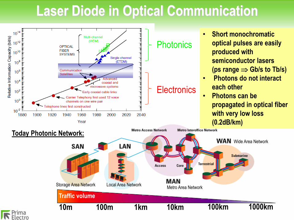
Laser Diode in Optical Communication
Photonics
Electronics
Today Photonic Network:
Storage Area Network Local Area Network
Wide Area Network
Metro Area Network
10km 100km100m10m 1km 1000km
Traffic volume
• Short monochromatic
optical pulses are easily
produced with
semiconductor lasers
(ps range Gb/s to Tb/s)
• Photons do not interact
each other
• Photons can be
propagated in optical fiber
with very low loss
(0.2dB/km)

III-V Devices Torino
Material Processing
Laser welding
Laser cutting
Laser drilling
Laser hardening
Laser microprocessing
Additive manufacturing
Sub
trac
tive
man
ufac
turin
g
Material processing efficiency is proportional to Laser Brightness:
• High Power
• High Beam Quality (Low BPP)
𝐵= 𝑃
𝜋2𝐵𝑃𝑃2

III-V Devices Torino
BPP required for material processing
III-V Devices Torino
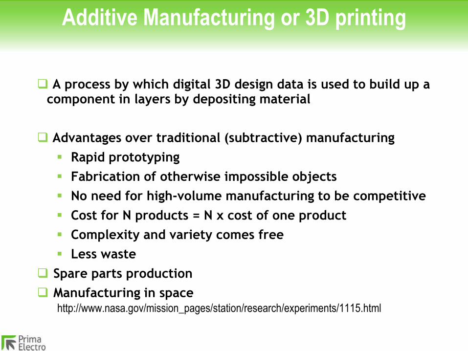
Additive Manufacturing or 3D printing
A process by which digital 3D design data is used to build up a component in layers by depositing material
Advantages over traditional (subtractive) manufacturing
Rapid prototyping
Fabrication of otherwise impossible objects
No need for high-volume manufacturing to be competitive
Cost for N products = N x cost of one product
Complexity and variety comes free
Less waste
Spare parts production
Manufacturing in space http://www.nasa.gov/mission_pages/station/research/experiments/1115.html

III-V Devices Torino
Laser Diode in Material Processing
Single laser diodes have optical power of the order of 10W and cannot be directly used for material processing, requiring several kW of optical power
Beam Coupling of many laser diodes intrinsically reduces the total beam quality thus preventing use for material processing
(BPPtot S BPPi )
Laser diode are typically used as pump sources for rare-earth-doped fiber lasers which in turn deliver the required kW optical power at low BPP
The low BPP recovery is achieved at the expense of optical power loss of about 40%

III-V Devices Torino
Fiber Laser
More than one hundreddiodes for 1kW out(high power at high BPP)
kW power
at low BPP
Active Fiber acts as a “BPP converter”
Optical Pumping
PinHigh BPP
Poutlow BPP
Fiber Laser Emission

III-V Devices Torino
Semiconductor Laser
Principle of Operation and Key Points
III-V Devices Torino
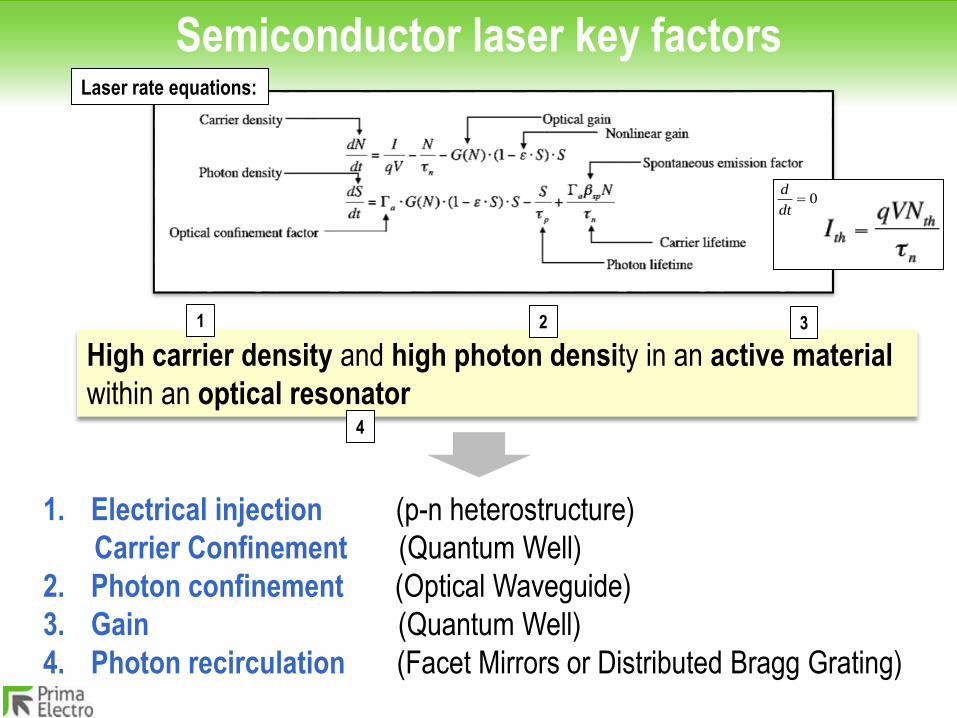
Semiconductor laser key factors
High carrier density and high photon density in an active material
within an optical resonator
1. Electrical injection (p-n heterostructure)
Carrier Confinement (Quantum Well)
2. Photon confinement (Optical Waveguide)
3. Gain (Quantum Well)
4. Photon recirculation (Facet Mirrors or Distributed Bragg Grating)
1 2 3
4
Laser rate equations:
0dt
d
III-V Devices Torino
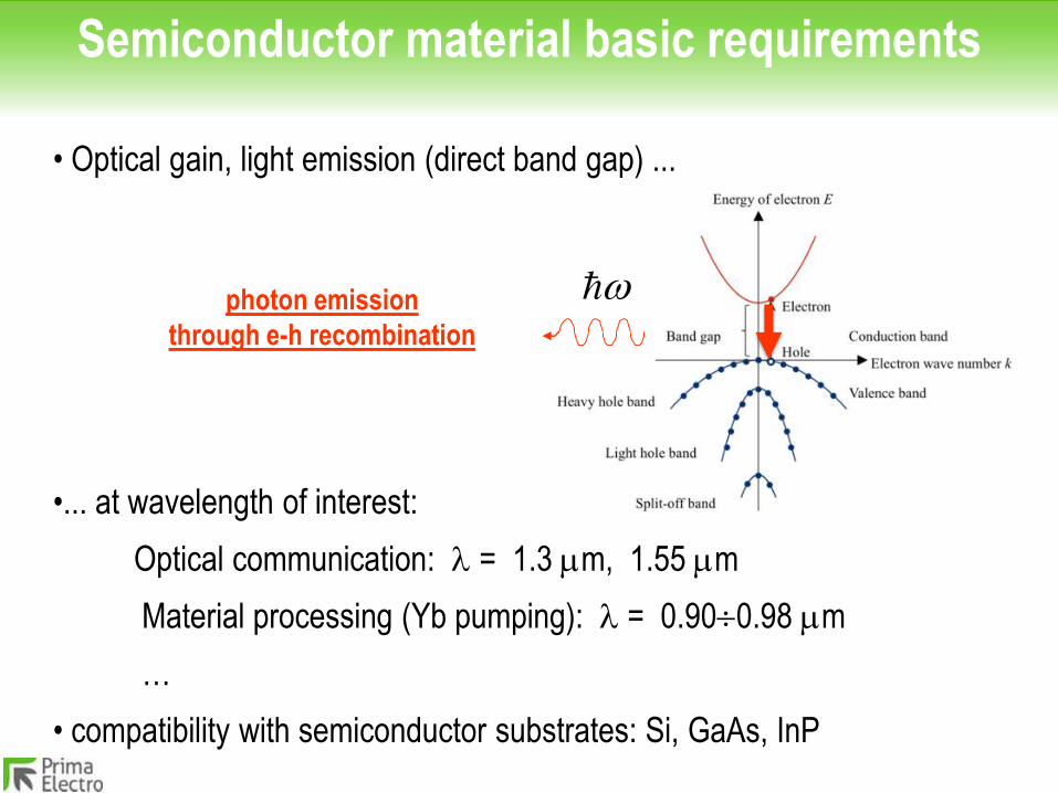
• Optical gain, light emission (direct band gap) ...
•... at wavelength of interest:
Optical communication: = 1.3 m, 1.55 m
Material processing (Yb pumping): = 0.900.98 m
…
• compatibility with semiconductor substrates: Si, GaAs, InP
Semiconductor material basic requirements
photon emission
through e-h recombination

III-V Devices Torino
III V
Semiconductor alloys of III-V elements are the best materials for semiconductor lasers emitting at wavelength of interest
III-V semiconductor materials

III-V Devices Torino
III-V alloys suited for the applications
T. P. Pearsall, , Wiley (1982)
In1-xGaxAsyP1-y alloy, grown on InP
substrate, covers the spectral
range required for optical telecom
Al1-xGaxAs (+ In1-xGaxAs) alloy,
grown on GaAs substrate, covers
the spectral range required for Yb-
fiber laser pumping
• High quality material
• Established
growth techniques
and material processing
InGaAs
AlAs
GaAsInP
InGaAs

III-V Devices Torino
(Basic) Optical properties of semiconductors
lhhh
e
E
Eg
**
**9
elh
ehh
mm
mm
Three bands are involved in optical transitions:
- Electrons Conduction Band
- Heavy holes
- Light holesValence Band
JDOS
Eg
a
gEJDOS
k
Joint density of states (available for optical
transitions) is a square root function of the
energy in excess of the energy gap

III-V Devices Torino
Semiconductor Heterostructures
A
(Substrate)
A
BB
A
Double Heterostructure (DH)
n
p
e-h confinement
Eg(A)> Eg(B)
Combination of layers of different crystalline semiconductors.
H. Kroemer, Varian associates 1963
(Nobel Prize in Physics, 2000)
The idea was experimentally demonstrated using the Liquid Phase Epitaxy (LPE)
Separate Confinement
Heterostructure (SCH)ph > e
A
(Substrate)
A
BB
A
n
p
Photon confinement
C
C
Eg(A)> Eg(C) )> Eg(B) , n(A)< n(C) < n(B)
refractive index
Yphoton

III-V Devices Torino
Quantum WellsQuantum-Size Double Heterostructure (Quantum Well) is a planar waveguide for electrons
C. H. Henry, Bell Labs 1972
The idea was experimentally demonstrated in 1974 using the newly developed Molecular
Beam Epitaxy (MBE).
A
QUANTUM WELL
d = 3
z
y
x
d = 2 Lw ~ e
BULK
EgAEg
B EgQW
1
2
21
B A B
Lw
QW is now a widely spread
quantum product
based in atomic-scale technology
B A B
Transmission Electron Microscope
view of QW

III-V Devices Torino
)()()(222
0
2
2znzznk
dz
deff
neff
2
Yph(z)
n2(z)
Photon wave eqn. vs. Electron wave eqn.
Helmholtz equation (photon)
refractive index ridges confine photons (optical waveguides)
zYe(z)
)()(2 zVzn
cladding barrier
core well
)()()(2 2
22
zEzzVdz
d
m
E
V(z)
Schroedinger equation (electron)
potential wells confine electrons (quantum wells)
III-V Devices Torino
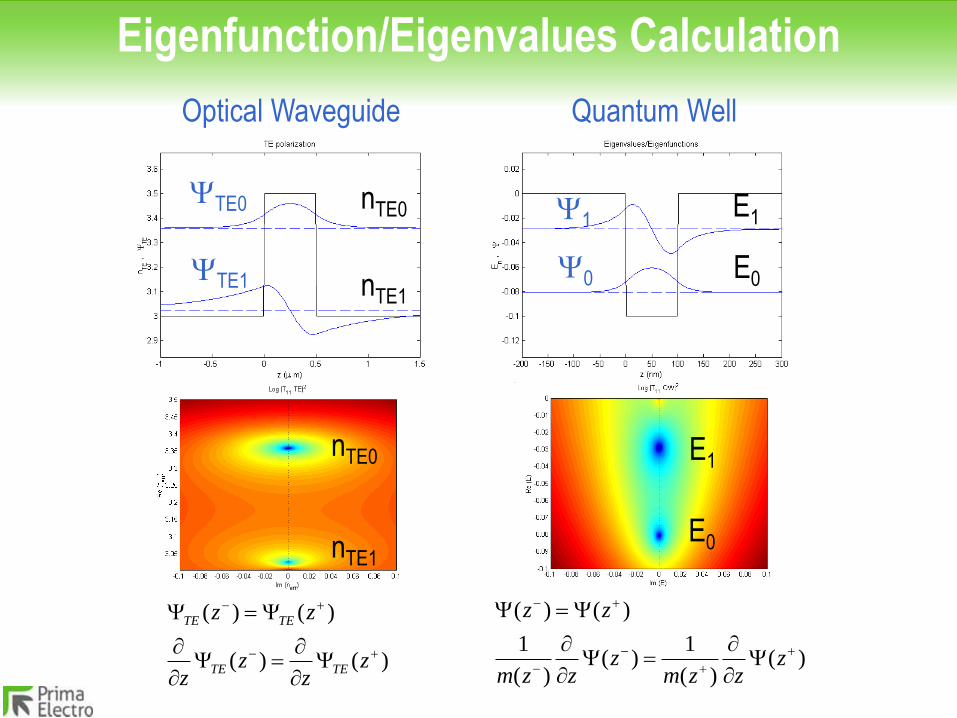
Eigenfunction/Eigenvalues Calculation
nTE0
nTE1
nTE0
nTE1
YTE0
YTE1
Optical Waveguide
)()(
)()(
Y
Y
YY
zz
zz
zz
TETE
TETE
E0
E1
E0
E1Y1
Y0
Quantum Well
)()(
1)(
)(
1
)()(
Y
Y
YY
zzzm
zzzm
zz
III-V Devices Torino QW band structure
E
hh1
e1
e2
hh2
lh2
lh1
11 1’1
TETM
22
z
Strong carrier confinement and
2D Joint Density of States (JDOS):
• Low laser threshold
• High thermal operation
• High differential gain
• Wide gain bandwith
• . . .
JDOS
e1-h
h1
EgQW
Egbulk
e1-l
h1
e2-h
h2
One step for
every
allowed
transition
( ) ji
ji
jiEJDOS
2
bulk
gEE
III-V Devices Torino
aL
aS
ma a
a
a lattice parameter of epitaxial layer
a lattice parameter of substrateL S
S
L
S
RST
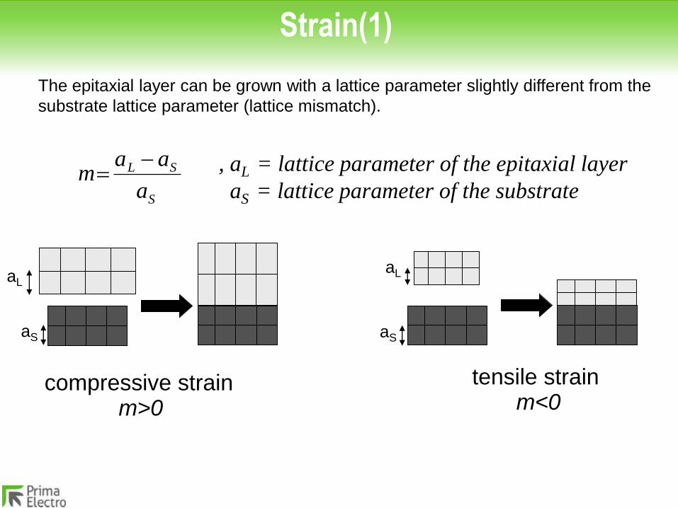
Strain(1)
The epitaxial layer can be grown with a lattice parameter slightly different from the
substrate lattice parameter (lattice mismatch).
compressive strainm>0
tensile strain
aL
aS
m<0
, aL = lattice parameter of the epitaxial layer
aS = lattice parameter of the substrate

III-V Devices Torino
T. P. Pearsall, , Wiley (1982)
InGaAs
InP
Strain(2)
±1%
AlAs
GaAs
InGaAs
InP
InGaAs
±1%GaAs
AlAs

III-V Devices Torino
hh1
e1
e2
lh1
11 1’1
k
E
lhhh
e
m=0
TM
TE
Strain effect on band structure:
lh1
k
E
lhhh
e
m>0
hh1
e1
e2
11 1’1
TM
TE
Low escape time
High T0 (low thermal dependence)
compressive
strain
k
E
lhhh
e
m<0
hh1
e1
e2
lh1
11 1’1
TE, TM
Low dichroism
Polarization-independent devices
tensile
strainunstrained
III-V Devices Torino
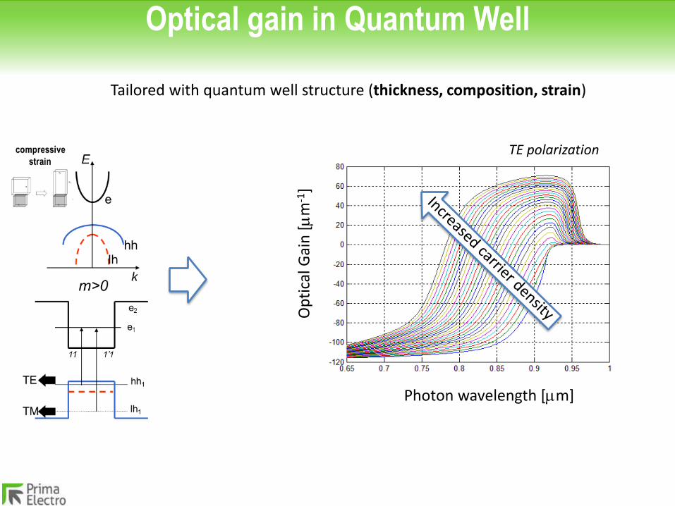
Op
tica
l Gai
n[
m-1
]
Photon wavelength [m]
Optical gain in Quantum Well
Optical gain
TE polarization
Tailored with quantum well structure (thickness, composition, strain)
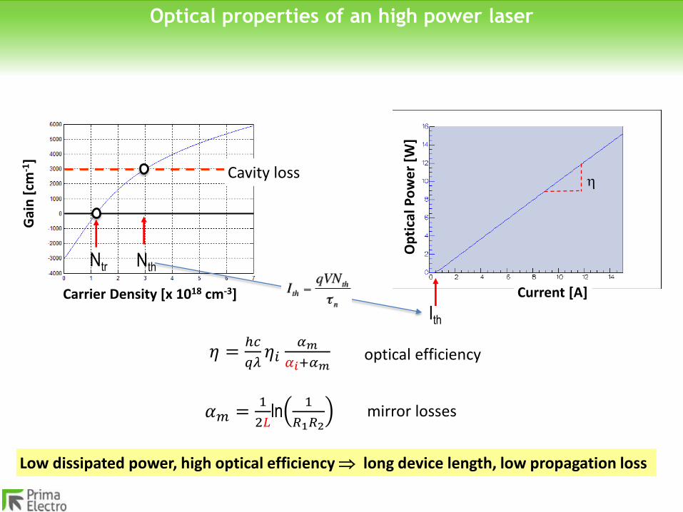
III-V Devices Torino Optical properties of an high power laser
𝜂 =ℎ𝑐
𝑞𝜆𝜂𝑖
𝛼𝑚
𝛼𝑖+𝛼𝑚
𝛼𝑚 =1
2𝐿ln
1
𝑅1𝑅2
h
Ith
mirror losses
optical efficiency
Op
tica
l Po
we
r [W
]
Current [A]
Low dissipated power, high optical efficiency long device length, low propagation loss
Carrier Density [x 1018 cm-3]
Gai
n[c
m-1
]
NthNtr
Cavity loss

III-V Devices Torino
Optical Confinement
x
n
Vertical Confinement
Lateral Confinement
Optical Waveguide
w
w
High-power laser:• single mode in transverse
direction (),w 1m , M
2 1• multimode in lateral
direction,w|| 100m, M ||
2 5

III-V Devices Torino
Fabry Perot Laser (FP): Multi (longitudinal) mode
L Nn
2
N= integer
n=refractive index
= wavelength
Cavity modes
Cavity mirrors are due to refractive index
discontinuity from semiconductor active
layer (n~3.2) and air
1280 1285 1290 1295 1300 1305
-70
-60
-50
-40
-30
-20
Wavelength (nm)
Am
pli
tud
e (
dB
m)
Device:br00T20u; I = 30.0 mA; Peak: 1291.0 nm; 23-Jan-2003
Lng2
2
Multi-mode emission
III-V Devices Torino
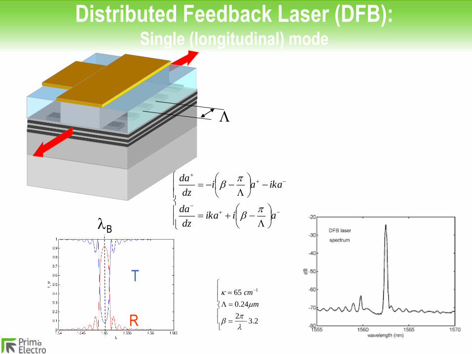
Distributed Feedback Laser (DFB):Single (longitudinal) mode
a+
a-
T
R
B
2.32
24.0
65 1
m
cm
aiikadz
da
ikaaidz
da

III-V Devices Torino
ATOMS
SEMICONDUCTOR LASER
Quantum Wells: Atomic-Controlled Artificial Structures
ACTIVE LAYER MQW
QUANTUM WELL
BARRIER
)()()(2 2
22
zEzzVdz
d
m
),,(),,( FNkiFNn
Control of Optical Properties through atomic-scale technology
Quantum Well requires sub-monolayer manufacturing control (s < 0.1nm over 10cm2 )
achievable with Molecular Beam Epitaxy or Metal Organic Chemical Vapor Deposition.

ELECTRONICS and LASER TECHNOLOGIESCompany Snapshot
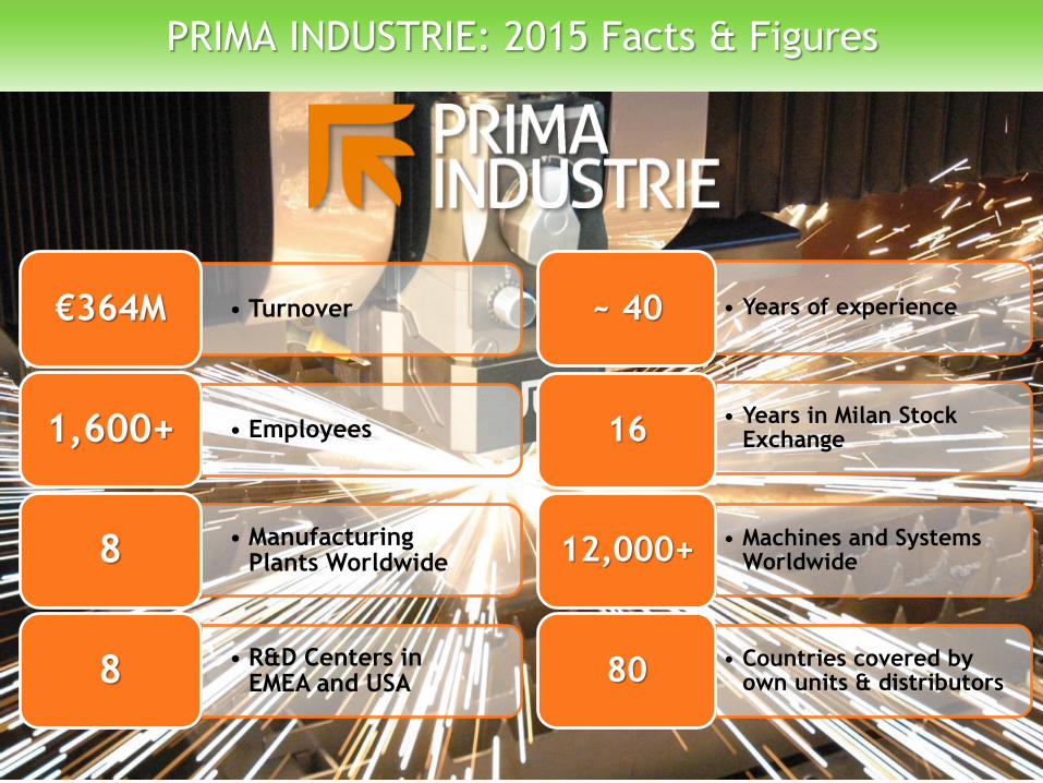
PRIMA INDUSTRIE: 2015 Facts & Figures
• Turnover€364M
• Employees1,600+
• Manufacturing Plants Worldwide8
• R&D Centers in EMEA and USA8
• Years of experience~ 40
• Years in Milan Stock Exchange 16
• Machines and Systems Worldwide12,000+
• Countries covered by own units & distributors80

PI Group Divisions
Machinery Division
Industrial grade dedicated electronics, numerical
controls & motions systems and high power laser
sources for industrial applications.
Electronic Division
Laser and sheet metal fabrication machinery: 3D
laser cutting, welding/drilling, punching, combined tech, bending, automation and FMS.

III-V Devices Torino
PI worldwide
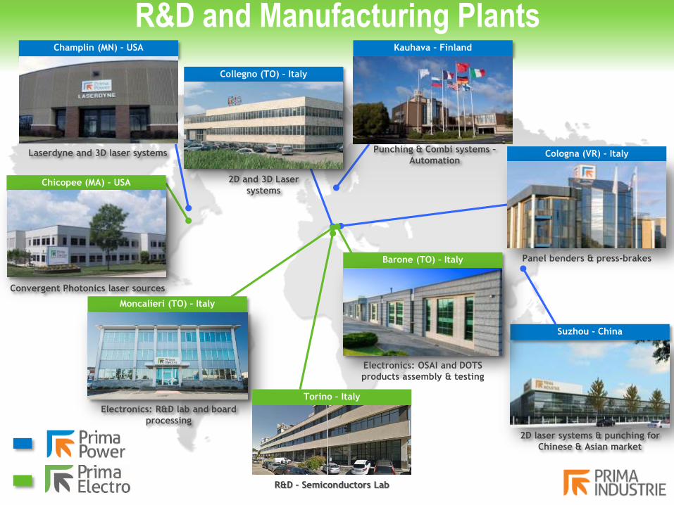
R&D and Manufacturing Plants
2D laser systems & punching for
Chinese & Asian market
Suzhou - China
Moncalieri (TO) – Italy
Convergent Photonics laser sources
Chicopee (MA) – USA
Electronics: R&D lab and board
processing
Barone (TO) – Italy
Punching & Combi systems –
Automation
Kauhava – Finland
2D and 3D Laser
systems
Collegno (TO) – Italy
Panel benders & press-brakes
Cologna (VR) – ItalyLaserdyne and 3D laser systems
Champlin (MN) – USA
Torino – Italy
R&D – Semiconductors Lab
Electronics: OSAI and DOTS
products assembly & testing
III-V Devices Torino
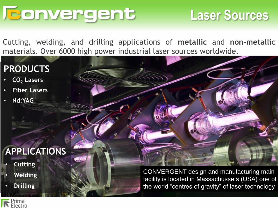
Laser Sources
PRODUCTS• CO2 Lasers
• Fiber Lasers
• Nd:YAG
APPLICATIONS
• Cutting
• Welding
• Drilling
Cutting, welding, and drilling applications of metallic and non-metallic
materials. Over 6000 high power industrial laser sources worldwide.
CONVERGENT design and manufacturing main
facility is located in Massachussets (USA) one of
the world “centres of gravity” of laser technology
III-V Devices Torino
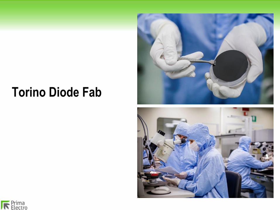
Torino Diode Fab
44

III-V Devices Torino
Production lasers in Torino (2007 - 2014)
2 Million diodes shipped to product line
Proven reliability:
No return from field
70 M device x hours tested in Lab
Team heritage is a long path of Research, Development and Production of Photonic devices for telecom
• As Optical Technology Research Center for Telecom Italia (CSELT – Tilab) since 1980; from 2000 to 2014 as R&D and Production center for Agilent / Avago technologies
• Developing know how on modeling, EPI growth and Technology Processes on semiconductor for Photonic devices
• 2007 - 2014, developing key competences on production engineering for telecom laser sources
Diode Fab Team R&D and Production
background
Telecom Italia Research Center “CSELT”
Optoelectronics Modules and Photonic Integrated Circuits
1980 1990 2000 2010
Team History
CSELT Agilent - Avago
2000 2010
Wide TunableLasers
FP Laser
EML
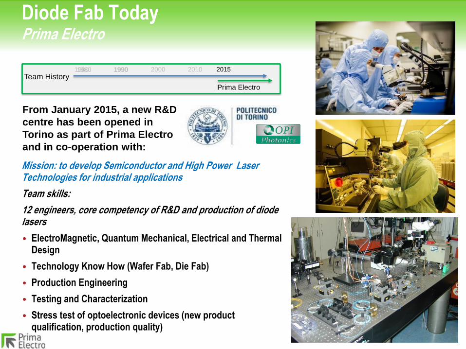
III-V Devices TorinoDiode Fab TodayPrima Electro
Mission: to develop Semiconductor and High Power Laser Technologies for industrial applications
Team skills:
12 engineers, core competency of R&D and production of diode lasers
• ElectroMagnetic, Quantum Mechanical, Electrical and ThermalDesign
• Technology Know How (Wafer Fab, Die Fab)
• Production Engineering
• Testing and Characterization
• Stress test of optoelectronic devices (new product qualification, production quality)
Prima Electro
1980 1990 2000 2010
Team History2015
From January 2015, a new R&D
centre has been opened in
Torino as part of Prima Electro
and in co-operation with:
1980 1990

III-V Devices Torino Semiconductor Lab
Facilities
Site Numbers:
Clean Rooms (10 -10000 class):
– 800 m2 Wafer Fab:
– 400 m2 Die Fab, Testing:
Stress Test (reliability): 100 m2
600 m2 of R&D Lab for Diode Laser testing, offices, meeting Room
Facilities:
Dielectric and metal deposition, wet and dry etching, nano-scale Lithography (EBL)
Automatic testing, Wafer Scribing, Chip-on-Carrier assembly
Stress tests and wafer validation (Burn In , Lifetest)
Multiemitter modules assembly line (2016)
Die Fab clean room
Wafer Fab clean room

III-V Devices Torino
photoresist
SiN
1) Photolithography
2) Chemical etch
UV
light
mask
How to make laser diodes:
Wafer process

III-V Devices Torino
Wafer bars Coating /cleave Laser Chips
Scribing Dicing
How to make laser diodes:
Die Process: from wafers to chips
0.6mm(w) x 5mm(L) x 0.1mm(h)


![HOME []...TORINO TORINO - TORINO - TORINO - TORINO - 22/09/1973 17/01/1963 26/03/1961 04/12/1976 21/05/1975 IL PRESIDENTE della Commissione Elettorale LA DIRIGENTE SCOLASTICA Prof.ssa](https://static.fdocuments.in/doc/165x107/5f2d1d51d15f88246835f084/home-torino-torino-torino-torino-torino-22091973-17011963-26031961.jpg)