High-Performance Impact Programmable Array Logic Circuits...
22
TIBPAL22V10C, TIBPAL22V10AC, TIBPAL22V10AM HIGH-PERFORMANCE IMPACT™ PROGRAMMABLE ARRAY LOGIC CIRCUITS SRPS024A - OCTOBER 1986 - REVISED APRIL 2010 POST OFFICE BOX 655303 • DALLAS, TEXAS 75265 Copyright © 2010, Texas Instruments Incorporated 1 PRODUCTION DATA information is current as of publication date. Products conform to specifications per the terms of Texas Instruments standard warranty. Production processing does not necessarily include testing of all parameters. • Second-Generation PLD Architecture • Choice of Operating Speeds TIBPAL22V10AC . . . 25 ns Max TIBPAL22V10AM . . . 30 ns Max TIBPAL22V10C . . . 35 ns Max • Increased Logic Power - Up to 22 Inputs and 10 Outputs • Increased Product Terms - Average of 12 Per Output • Variable Product Term Distribution Allows More Complex Functions to Be Implemented • Each Output Is User Programmable for Registered or Combinational Operation, Polarity, and Output Enable Control • TTL-Level Preload for Improved Testability • Extra Terms Provide Logical Synchronous Set and Asynchronous Reset Capability • Fast Programming, High Programming Yield, and Unsurpassed Reliability Ensured Using Ti-W Fuses • AC and DC Testing Done at the Factory Utilizing Special Designed-In Test Features • Dependable Texas Instruments Quality and Reliability • Package Options Include Both Plastic and Ceramic Chip Carriers in Addition to Plastic and Ceramic DIPs • Functionally Equivalent to AMDs AMPAL22V10 and AMPAL22V10A description The TIBPAL22V10 and TIBPAL22V10A are programmable array logic devices featuring high speed and functional equivalency when compared to presently available devices. They are implemented with the familiar sum-of-products (AND-OR) logic structure featuring the new concept “Programmable Output Logic Macrocell”. These IMPACT ™ circuits combine the latest Advanced Low-Power Schottky technology with proven titanium-tungsten fuses to provide reliable, high-performance substitutes for conventional TTL logic. These devices contain up to 22 inputs and 10 outputs. They incorporate the unique capability of defining and programming the architecture of each output on an individual basis. Outputs may be registered or nonregistered and inverting or noninverting as shown in the output logic macrocell diagram. The ten potential outputs are enabled through the use of individual product terms. These devices are covered by U.S. Patent 4,410,987. IMPACT is a trademark of Texas Instruments Incorporated. 1 2 3 4 5 6 7 8 9 10 11 12 24 23 22 21 20 19 18 17 16 15 14 13 CLK/I I I I I I I I I I I GND V CC I/O/Q I/O/Q I/O/Q I/O/Q I/O/Q I/O/Q I/O/Q I/O/Q I/O/Q I/O/Q I C SUFFIX . . . NT PACKAGE M SUFFIX . . . JT OR W PACKAGE (TOP VIEW) 3 2 1 28 27 12 13 5 6 7 8 9 10 11 25 24 23 22 21 20 19 I/O/Q I/O/Q I/O/Q NC I/O/Q I/O/Q I/O/Q I I I NC I I I 4 26 14 15 16 17 18 I I GND NC I I/O/Q I/O/Q I I CLK/I NC I/O/Q I/O/Q C SUFFIX . . . FN PACKAGE M SUFFIX . . . FK PACKAGE (TOP VIEW) NC - No internal connection Pin assignments in operating mode V CC TIBPAL22V10AM is Not Recommended For New Designs
Transcript of High-Performance Impact Programmable Array Logic Circuits...

TIBPAL22V10C, TIBPAL22V10AC, TIBPAL22V10AMHIGH-PERFORMANCE IMPACT�™ PROGRAMMABLE ARRAY LOGIC CIRCUITS
SRPS024A − OCTOBER 1986 − REVISED APRIL 2010
POST OFFICE BOX 655303 • DALLAS, TEXAS 75265
Copyright © 2010, Texas Instruments Incorporated
1
PRODUCTION DATA information is current as of publication date.Products conform to specifications per the terms of Texas Instrumentsstandard warranty. Production processing does not necessarily includetesting of all parameters.
• Second-Generation PLD Architecture
• Choice of Operating SpeedsTIBPAL22V10AC . . . 25 ns MaxTIBPAL22V10AM . . . 30 ns MaxTIBPAL22V10C . . . 35 ns Max
• Increased Logic Power − Up to 22 Inputsand 10 Outputs
• Increased Product Terms − Average of 12Per Output
• Variable Product Term Distribution Allows More Complex Functions to BeImplemented
• Each Output Is User Programmable forRegistered or Combinational Operation,Polarity, and Output Enable Control
• TTL-Level Preload for Improved Testability
• Extra Terms Provide Logical SynchronousSet and Asynchronous Reset Capability
• Fast Programming, High ProgrammingYield, and Unsurpassed Reliability EnsuredUsing Ti-W Fuses
• AC and DC Testing Done at the FactoryUtilizing Special Designed-In Test Features
• Dependable Texas Instruments Quality andReliability
• Package Options Include Both Plastic andCeramic Chip Carriers in Addition to Plasticand Ceramic DIPs
• Functionally Equivalent to AMDsAMPAL22V10 and AMPAL22V10A
description
The TIBPAL22V10 and TIBPAL22V10A are programmable array logic devices featuring high speed andfunctional equivalency when compared to presently available devices. They are implemented with the familiarsum-of-products (AND-OR) logic structure featuring the new concept “Programmable Output Logic Macrocell”.These IMPACT™ circuits combine the latest Advanced Low-Power Schottky technology with proventitanium-tungsten fuses to provide reliable, high-performance substitutes for conventional TTL logic.
These devices contain up to 22 inputs and 10 outputs. They incorporate the unique capability of defining andprogramming the architecture of each output on an individual basis. Outputs may be registered or nonregisteredand inverting or noninverting as shown in the output logic macrocell diagram. The ten potential outputs areenabled through the use of individual product terms.
These devices are covered by U.S. Patent 4,410,987.IMPACT is a trademark of Texas Instruments Incorporated.
1
2
3
4
5
6
7
8
9
10
11
12
24
23
22
21
20
19
18
17
16
15
14
13
CLK/IIIIIIIIIII
GND
VCCI/O/QI/O/QI/O/QI/O/QI/O/QI/O/QI/O/QI/O/QI/O/QI/O/QI
C SUFFIX . . . NT PACKAGEM SUFFIX . . . JT OR W PACKAGE
(TOP VIEW)
3 2 1 28 27
12 13
5
6
7
8
9
10
11
25
24
23
22
21
20
19
I/O/QI/O/QI/O/QNCI/O/QI/O/QI/O/Q
III
NCIII
4 26
14 15 16 17 18
I IG
ND
NC I
I/O/Q
I/O/Q
I I CLK
/IN
C
I/O/Q
I/O/Q
C SUFFIX . . . FN PACKAGEM SUFFIX . . . FK PACKAGE
(TOP VIEW)
NC − No internal connectionPin assignments in operating mode
V CC
TIBPAL22V10AM is Not Recommended For New Designs

TIBPAL22V10C, TIBPAL22V10AC, TIBPAL22V10AMHIGH-PERFORMANCE IMPACT�™ PROGRAMMABLE ARRAY LOGIC CIRCUITS
SRPS024A − OCTOBER 1986 − REVISED APRIL 2010
POST OFFICE BOX 655303 • DALLAS, TEXAS 752652
description (continued)
Further advantages can be seen in the introduction of variable product term distribution. This techniqueallocates from 8 to 16 logical product terms to each output for an average of 12 product terms per output. Thisvariable allocation of terms allows far more complex functions to be implemented than in previously availabledevices.
Circuit design is enhanced by the addition of a synchronous set and an asynchronous reset product term. Thesefunctions are common to all registers. When the synchronous set product term is a logic 1, the output registersare loaded with a logic 1 on the next low-to-high clock transition. When the asynchronous reset product termis a logic 1, the output registers are loaded with a logic 0. The output logic level after set or reset depends onthe polarity selected during programming. Output registers can be preloaded to any desired state during testing.Preloading permits full logical verification during product testing.
With features such as programmable output logic macrocells and variable product term distribution, theTIBPAL22V10 and TIBPAL22V10A offer quick design and development of custom LSI functions withcomplexities of 500 to 800 equivalent gates. Since each of the ten output pins may be individually configuredas inputs on either a temporary or permanent basis, functions requiring up to 21 inputs and a single output ordown to 12 inputs and 10 outputs are possible.
A power-up clear function is supplied that forces all registered outputs to a predetermined state after power isapplied to the device. Registered outputs selected as active-low power up with their outputs high. Registeredoutputs selected as active-high power up with their outputs low.
A single security fuse is provided on each device to discourage unauthorized copying of fuse patterns. Onceblown, the verification circuitry is disabled and all other fuses will appear to be open.
The TIBPAL22V10C and TIBPAL22V10AC are characterized for operation from 0°C to 75°C. TheTIBPAL22V10AM is characterized for operation over the full military temperature range of −55°C to125°C.
TIBPAL22V10AM is Not Recommended For New Designs
TIBPAL22V10C, TIBPAL22V10AC, TIBPAL22V10AMHIGH-PERFORMANCE IMPACT�™ PROGRAMMABLE ARRAY LOGIC CIRCUITS
SRPS024A − OCTOBER 1986 − REVISED APRIL 2010
POST OFFICE BOX 655303 • DALLAS, TEXAS 75265 3
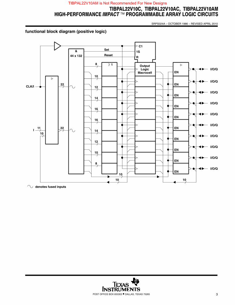
functional block diagram (positive logic)
I/O/Q
I/O/Q
I/O/Q
I/O/Q
I/O/Q
I/O/Q
10
12
14
EN
16
16
14
12
10
22
22
1
10
&
44 x 132
I/O/Q
I/O/Q
I/O/Q
I/O/Q
EN
EN
EN
EN
EN
EN
EN
EN
EN
10
10
8
8
10
11
CLK/I
I
Set
Reset1S
R
C1
denotes fused inputs
OutputLogic
Macrocell
TIBPAL22V10AM is Not Recommended For New Designs

TIBPAL22V10C, TIBPAL22V10AC, TIBPAL22V10AMHIGH-PERFORMANCE IMPACT�™ PROGRAMMABLE ARRAY LOGIC CIRCUITS
SRPS024A − OCTOBER 1986 − REVISED APRIL 2010
POST OFFICE BOX 655303 • DALLAS, TEXAS 752654
04
812
1620
2428
Incr
emen
ts
Fir
stF
use
Nu
mb
ers
3236
40
Mac
ro-
cell
R =
580
9P
= 5
808
R =
581
1P
= 5
810
R =
581
3P
= 5
812
R =
581
5P
= 5
814
R =
581
7P
= 5
816
log
ic s
ymb
ol (
po
siti
ve lo
gic
)
Asy
nch
ron
ou
s R
eset
23 22 21 20 19
1 2 3 4 5
(to
all
reg
iste
rs)
3960
440
880
924
1452
1496
2112
2156
2860
I/O/Q
I/O/Q
I/O/Q
I/O/Q
I/O/Q
IIII
CL
K/I
Mac
ro-
cell
Mac
ro-
cell
Mac
ro-
cell
Mac
ro-
cell
TIBPAL22V10AM is Not Recommended For New Designs

TIBPAL22V10C, TIBPAL22V10AC, TIBPAL22V10AMHIGH-PERFORMANCE IMPACT�™ PROGRAMMABLE ARRAY LOGIC CIRCUITS
SRPS024A − OCTOBER 1986 − REVISED APRIL 2010
POST OFFICE BOX 655303 • DALLAS, TEXAS 75265 5
Fus
e nu
mbe
r =
Firs
t fus
e nu
mbe
r +
Incr
emen
t
R =
581
9P
= 5
818
R =
582
1P
= 5
820
R =
582
3P
= 5
822
R =
582
5P
= 5
824
R =
582
7P
= 5
826
18
6 7 8 9 10 11
17 16 15 14
Syn
chro
no
us
Set
13(t
o a
ll re
gis
ters
)
Insi
de e
ach
MA
CR
OC
ELL
the
”P”
fuse
is th
e po
larit
y fu
se a
nd th
e ”R
” fu
se is
the
regi
ster
fuse
.
2904
3608
3652
4268
4312
4840
4884
5324
5368
5720
5764
I I I I I I
I/O/Q
I/O/Q
I/O/Q
I/O/Q
I/O/Q
I
Mac
ro-
cell
Mac
ro-
cell
Mac
ro-
cell
Mac
ro-
cell
Mac
ro-
cell
TIBPAL22V10AM is Not Recommended For New Designs

TIBPAL22V10C, TIBPAL22V10AC, TIBPAL22V10AMHIGH-PERFORMANCE IMPACT�™ PROGRAMMABLE ARRAY LOGIC CIRCUITS
SRPS024A − OCTOBER 1986 − REVISED APRIL 2010
POST OFFICE BOX 655303 • DALLAS, TEXAS 752656
output logic macrocell diagram
C1
G0
30
1
1
0
3
2MUX
I = 0
1S
1D
R
MUX
G1
1
1
SS
AR
From Clock Buffer
S1
S0
AR = asynchronous resetSS = synchronous set
Output Logic Macrocell
TIBPAL22V10AM is Not Recommended For New Designs

FEEDBACK AND OUTPUT CONFIGURATION
TIBPAL22V10C, TIBPAL22V10AC, TIBPAL22V10AMHIGH-PERFORMANCE IMPACT�™ PROGRAMMABLE ARRAY LOGIC CIRCUITS
SRPS024A − OCTOBER 1986 − REVISED APRIL 2010
POST OFFICE BOX 655303 • DALLAS, TEXAS 75265 7
C1
1S
1D
R
S1 = 0
S0 = 0
C1
1S
1D
R
S1 = 0
S0 = 1
REGISTER FEEDBACK, REGISTERED, ACTIVE-LOW OUTPUT REGISTER FEEDBACK, REGISTERED, ACTIVE-HIGH OUTPUT
S1 = 1
S0 = 0
S1 = 1
S0 = 1
I/O FEEDBACK, COMBINATIONAL, ACTIVE-LOW OUTPUT I/O FEEDBACK, COMBINATIONAL, ACTIVE-HIGH OUTPUT
MACROCELL FEEDBACK AND OUTPUT FUNCTION TABLE
FUSE SELECTS1 S0
0 0 Register feedback Registered Active low
0 1 Register feedback Registered Active high
1 0 I/O feedback Combinational Active low
1 1 I/O feedback Combinational Active high
0 = unblown fuse, 1 = blown fuseS1 and S0 are select-function fuses as shown in the output logic macrocelldiagram.
Figure 1. Resultant Macrocell Feedback and Output Logic After Programming
TIBPAL22V10AM is Not Recommended For New Designs

nsPulse durationtw
nstsu Setup time before clock↑
UNIT
TIBPAL22V10C, TIBPAL22V10ACHIGH-PERFORMANCE IMPACT�™ PROGRAMMABLE ARRAY LOGIC CIRCUITS
SRPS024A − OCTOBER 1986 − REVISED APRIL 2010
POST OFFICE BOX 655303 • DALLAS, TEXAS 752658
absolute maximum ratings over operating free-air temperature range (unless otherwise noted)
Supply voltage, VCC (see Note 1) 7 V. . . . . . . . . . . . . . . . . . . . . . . . . . . . . . . . . . . . . . . . . . . . . . . . . . . . . . . . . . . . Input voltage (see Note 1) −5.5 V. . . . . . . . . . . . . . . . . . . . . . . . . . . . . . . . . . . . . . . . . . . . . . . . . . . . . . . . . . . . . . . . . Voltage range applied to disabled output (see Note 1) 5.5 V. . . . . . . . . . . . . . . . . . . . . . . . . . . . . . . . . . . . . . . . . Operating free-air temperature range 0°C to 75°C. . . . . . . . . . . . . . . . . . . . . . . . . . . . . . . . . . . . . . . . . . . . . . . . . . Storage temperature range −65°C to 150°C. . . . . . . . . . . . . . . . . . . . . . . . . . . . . . . . . . . . . . . . . . . . . . . . . . . . . . . .
NOTE 1: These ratings apply except for programming pins during a programming cycle or during a preload cycle.
recommended operating conditionsTIBPAL22V10C TIBPAL22V10AC
MIN NOM MAX MIN NOM MAX
VCC Supply voltage 4.75 5 5.25 4.75 5 5.25 V
VIH High-level input voltage 2 5.5 2 5.5 V
VIL Low-level input voltage 0.8 0.8 V
IOH High-level output current −3.2 −3.2 mA
IOL Low-level output current 16 16 mA
fclock Clock frequency† 18 28.5 MHz
Clock high or low 25 15
Asynchronous reset high or low 35 25
Input 30 20
Feedback 30 20
Synchronous set 30 25
Asynchronous reset low (inactive) 35 25
th Hold time, input, set, or feedback after clock↑ 0 0 ns
TA Operating free-air temperature 0 75 0 75 °C
† fclock (with feedback) = 1tsu � tpd(CLK to Q)
, fclock (without feedback) = 1tw(low) � tw(high)
TIBPAL22V10AM is Not Recommended For New Designs

IIL VCC = 5.25 V, VI = 0.4 V μA
UNITTEST CONDITIONSPARAMETER
TEST CONDITIONSPARAMETER UNIT
TIBPAL22V10C, TIBPAL22V10ACHIGH-PERFORMANCE IMPACT�™ PROGRAMMABLE ARRAY LOGIC CIRCUITS
SRPS024A − OCTOBER 1986 − REVISED APRIL 2010
POST OFFICE BOX 655303 • DALLAS, TEXAS 75265 9
electrical characteristics over recommended operating free-air temperature range
TIBPAL22V10C TIBPAL22V10AC
MIN TYP† MAX MIN TYP† MAX
VIK VCC = 4.75 V, II = −18 mA −1.2 −1.2 V
VOH VCC = 4.75 V, IOH = −3.2 mA 2.4 3.5 2.4 3.5 V
VOL VCC = 4.75 V, IOL = 16 mA 0.35 0.5 0.35 0.5 V
IOZH VCC = 5.25 V, VO = 2.7 V 0.1 0.1 mA
Any output −100 −100
Any I/O −250 −250
II VCC = 5.25 V, VI = 5.5 V 1 1 mA
IIH VCC = 5.25 V, VI = 2.7 V 25 25 μA
IIL VCC = 5.25 V, VI = 0.4 V −0.25 −0.25 mA
IOS‡ VCC = 5.25 V, VO = 0.5 V −30 −90 −30 −90 mA
ICC VCC = 5.25 V, VI = GND, Outputs open 120 180 120 180 mA
switching characteristics over recommended ranges of supply voltage and operating free-airtemperature (unless otherwise noted)
FROM TO TIBPAL22V10C TIBPAL22V10AC
(INPUT) (OUTPUT) MIN TYP† MAX MIN TYP† MAX
fmax¶ With feedback 18 28.5 MHz
tpd I, I/O I/O R1 = 300 Ω, 15 35 15 25 ns
tpd I, I/O (reset) Q R2 = 390 Ω, 15 40 15 30 ns
tpd CLK Q See Figure 4 10 25 10 15 ns
ten I, I/O I/O, Q 15 35 15 25 ns
tdis I, I/O I/O, Q 15 35 15 25 ns
† All typical values are at VCC = 5 V, TA = 25°C.‡ Not more than one output should be shorted at a time, and the duration of the short circuit should not exceed one second. VO is set at 0.5 V to
avoid test problems caused by test equipment ground degradation.
¶ fmax (with feedback) = 1tsu � tpd(CLK to Q)
, fmax (without feedback) = 1tw(low) � tw(high)
TIBPAL22V10AM is Not Recommended For New Designs

nsPulse durationtw
nstsu Setup time before clock↑
TIBPAL22V10AMHIGH-PERFORMANCE IMPACT�™ PROGRAMMABLE ARRAY LOGIC CIRCUITS
SRPS024A − OCTOBER 1986 − REVISED APRIL 2010
POST OFFICE BOX 655303 • DALLAS, TEXAS 7526510
absolute maximum ratings over operating free-air temperature range (unless otherwise noted)
Supply voltage, VCC (see Note 1) 7 V. . . . . . . . . . . . . . . . . . . . . . . . . . . . . . . . . . . . . . . . . . . . . . . . . . . . . . . . . . . . Input voltage (see Note 1) −5.5 V. . . . . . . . . . . . . . . . . . . . . . . . . . . . . . . . . . . . . . . . . . . . . . . . . . . . . . . . . . . . . . . . . Voltage range applied to disabled output (see Note 1) 5.5 V. . . . . . . . . . . . . . . . . . . . . . . . . . . . . . . . . . . . . . . . . Operating free-air temperature range −55°C to 125°C. . . . . . . . . . . . . . . . . . . . . . . . . . . . . . . . . . . . . . . . . . . . . . . Storage temperature range −65°C to 150°C. . . . . . . . . . . . . . . . . . . . . . . . . . . . . . . . . . . . . . . . . . . . . . . . . . . . . . . .
NOTE 1: These ratings apply except for programming pins during a programming cycle or during a preload cycle.
recommended operating conditionsMIN NOM MAX UNIT
VCC Supply voltage 4.5 5 5.5 V
VIH High-level input voltage 2 5.5 V
VIL Low-level input voltage 0.8 V
IOH High-level output current −2 mA
IOL Low-level output current 12 mA
fclock Clock frequency† 22 MHz
Clock high or low 20
Asynchronous reset high or low 30
Input 25
Feedback 25
Synchronous set 25
Asynchronous reset low (inactive) 30
th Hold time, input, set, or feedback after clock↑ 0 ns
TA Operating free-air temperature −55 125 °C
† fclock (with feedback) = 1tsu � tpd(CLK to Q)
, fclock (without feedback) = 1tw(low) � tw(high)
TIBPAL22V10AM is Not Recommended For New Designs
TIBPAL22V10AMHIGH-PERFORMANCE IMPACT�™ PROGRAMMABLE ARRAY LOGIC CIRCUITS
SRPS024A − OCTOBER 1986 − REVISED APRIL 2010
POST OFFICE BOX 655303 • DALLAS, TEXAS 75265 11
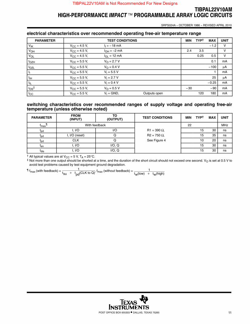
electrical characteristics over recommended operating free-air temperature range
PARAMETER TEST CONDITIONS MIN TYP† MAX UNIT
VIK VCC = 4.5 V, II = −18 mA −1.2 V
VOH VCC = 4.5 V, IOH = −2 mA 2.4 3.5 V
VOL VCC = 4.5 V, IOL = 12 mA 0.25 0.5 V
IOZH VCC = 5.5 V, VO = 2.7 V 0.1 mA
IOZL VCC = 5.5 V, VO = 0.4 V −100 μA
II VCC = 5.5 V, VI = 5.5 V 1 mA
IIH VCC = 5.5 V, VI = 2.7 V 25 μA
IIL VCC = 5.5 V, VI = 0.4 V −0.25 mA
IOS‡ VCC = 5.5 V, VO = 0.5 V −30 −90 mA
ICC VCC = 5.5 V, VI = GND, Outputs open 120 180 mA
switching characteristics over recommended ranges of supply voltage and operating free-airtemperature (unless otherwise noted)
PARAMETERFROM
(INPUT)TO
(OUTPUT) TEST CONDITIONS MIN TYP† MAX UNIT
fmax¶ With feedback 22 MHz
tpd I, I/O I/O R1 = 390 Ω, 15 30 ns
tpd I, I/O (reset) Q R2 = 750 Ω, 15 35 ns
tpd CLK Q See Figure 4 10 20 ns
ten I, I/O I/O, Q 15 30 ns
tdis I, I/O I/O, Q 15 30 ns
† All typical values are at VCC = 5 V, TA = 25°C.‡ Not more than one output should be shorted at a time, and the duration of the short circuit should not exceed one second. VO is set at 0.5 V to
avoid test problems caused by test equipment ground degradation.
¶ fmax (with feedback) = 1tsu � tpd(CLK to Q)
, fmax (without feedback) = 1tw(low) � tw(high)
TIBPAL22V10AM is Not Recommended For New Designs

TIBPAL22V10C, TIBPAL22V10AC, TIBPAL22V10AMHIGH-PERFORMANCE IMPACT�™ PROGRAMMABLE ARRAY LOGIC CIRCUITS
SRPS024A − OCTOBER 1986 − REVISED APRIL 2010
POST OFFICE BOX 655303 • DALLAS, TEXAS 7526512
preload procedure for registered outputs (see Notes 2 and 3)
The output registers can be preloaded to any desired state during device testing. This permits any state to betested without having to step through the entire state-machine sequence. Each register is preloaded individuallyby following the steps given below:
Step 1. With VCC at 5 V and pin 1 at VIL, raise pin 13 to VIHH.Step 2. Apply either VIL or VIH to the output corresponding to the register to be preloaded.Step 3. Pulse pin 1, clocking in preload data.Step 4. Remove output voltage, then lower pin 13 to VIL. Preload can be verified by observing the voltage level
at the output pin.
tdtsu
twtd
VIHH
VIL
VIL
VOL
VOH
VIH
Pin 13
Pin 1
Registered I/O Input OutputVIH
VIL
Figure 2. Preload Waveforms
NOTES: 2. Pin numbers shown are for JT and NT packages only. If chip-carrier socket adapter is not used, pin numbers must be changedaccordingly.
3. td = tsu = tw = 100 ns to 1000 ns. VIHH = 10.25 V to 10.75 V.
TIBPAL22V10AM is Not Recommended For New Designs
TIBPAL22V10C, TIBPAL22V10AC, TIBPAL22V10AMHIGH-PERFORMANCE IMPACT�™ PROGRAMMABLE ARRAY LOGIC CIRCUITS
SRPS024A − OCTOBER 1986 − REVISED APRIL 2010
POST OFFICE BOX 655303 • DALLAS, TEXAS 75265 13
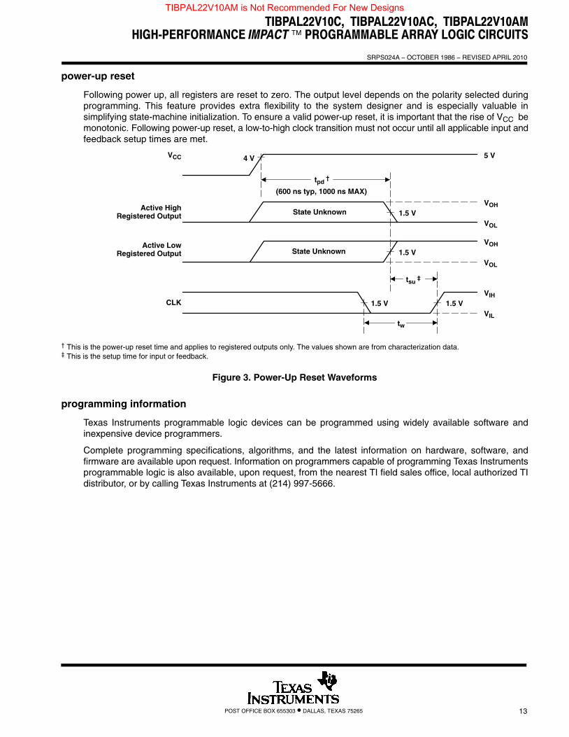
power-up reset
Following power up, all registers are reset to zero. The output level depends on the polarity selected duringprogramming. This feature provides extra flexibility to the system designer and is especially valuable insimplifying state-machine initialization. To ensure a valid power-up reset, it is important that the rise of VCC bemonotonic. Following power-up reset, a low-to-high clock transition must not occur until all applicable input andfeedback setup times are met.
1.5 V
tsu ‡
tpd †
tw
VOL
VOH
VIL
VIH
5 VVCC
Active HighRegistered Output
Active LowRegistered Output
CLK
4 V
VOH
VOL
1.5 V
1.5 V
(600 ns typ, 1000 ns MAX)
State Unknown
1.5 V
State Unknown
† This is the power-up reset time and applies to registered outputs only. The values shown are from characterization data.‡ This is the setup time for input or feedback.
Figure 3. Power-Up Reset Waveforms
programming information
Texas Instruments programmable logic devices can be programmed using widely available software andinexpensive device programmers.
Complete programming specifications, algorithms, and the latest information on hardware, software, andfirmware are available upon request. Information on programmers capable of programming Texas Instrumentsprogrammable logic is also available, upon request, from the nearest TI field sales office, local authorized TIdistributor, or by calling Texas Instruments at (214) 997-5666.
TIBPAL22V10AM is Not Recommended For New Designs
TIBPAL22V10C, TIBPAL22V10AC, TIBPAL22V10AMHIGH-PERFORMANCE IMPACT�™ PROGRAMMABLE ARRAY LOGIC CIRCUITS
SRPS024A − OCTOBER 1986 − REVISED APRIL 2010
POST OFFICE BOX 655303 • DALLAS, TEXAS 7526514
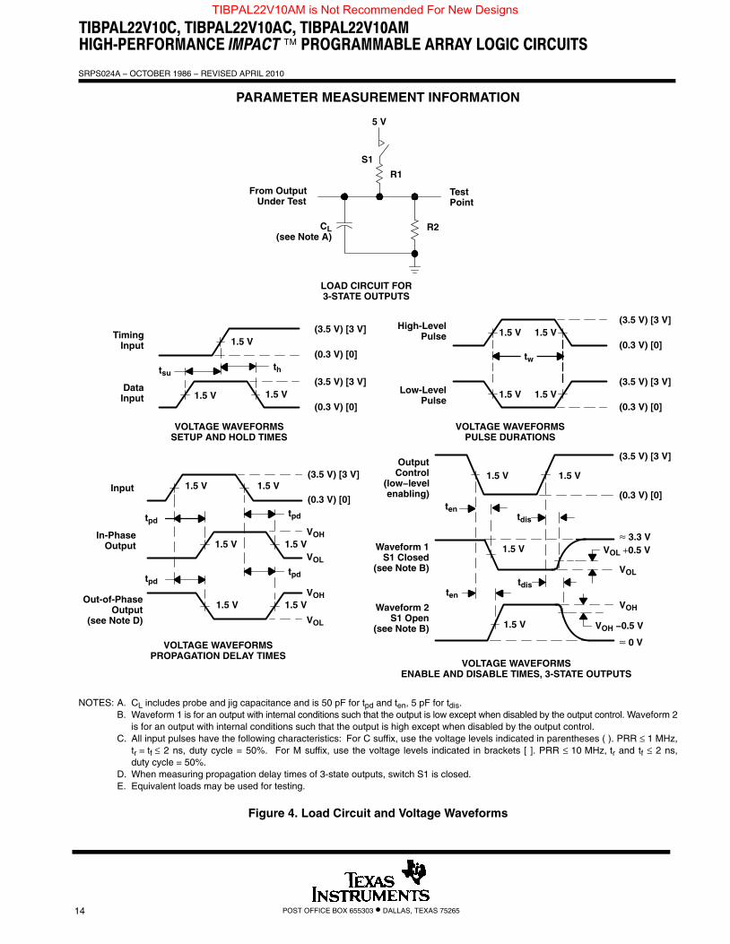
PARAMETER MEASUREMENT INFORMATION
tsu
S1
R2CL(see Note A)
LOAD CIRCUIT FOR3-STATE OUTPUTS
(3.5 V) [3 V]
(0.3 V) [0]
1.5 V
1.5 V
th
1.5 V
tpd
tpd
tpd
tpd
VOLTAGE WAVEFORMSSETUP AND HOLD TIMES
VOLTAGE WAVEFORMSPROPAGATION DELAY TIMES
VOH
VOH
VOL
VOL
1.5 V 1.5 V
1.5 V 1.5 V
tw
1.5 V 1.5 V
≈ 3.3 V
VOL
VOH
VOH −0.5 V
≈ 0 V
ten
ten
tdis
tdis
VOLTAGE WAVEFORMSENABLE AND DISABLE TIMES, 3-STATE OUTPUTS
VOLTAGE WAVEFORMSPULSE DURATIONS
1.5 V 1.5 V
1.5 V
1.5 V 1.5 V
1.5 V 1.5 V
1.5 V
R1
VOL +0.5 V
5 V
(3.5 V) [3 V]
(0.3 V) [0]
(3.5 V) [3 V]
(0.3 V) [0]
(3.5 V) [3 V]
(0.3 V) [0]
(3.5 V) [3 V]
(0.3 V) [0]
(3.5 V) [3 V]
(0.3 V) [0]
From Output Under Test
TestPoint
Input
Out-of-PhaseOutput
(see Note D)
TimingInput
DataInput
In-PhaseOutput
High-LevelPulse
Low-LevelPulse
OutputControl
(low−levelenabling)
Waveform 1S1 Closed
(see Note B)
Waveform 2S1 Open
(see Note B)
NOTES: A. CL includes probe and jig capacitance and is 50 pF for tpd and ten, 5 pF for tdis.B. Waveform 1 is for an output with internal conditions such that the output is low except when disabled by the output control. Waveform 2
is for an output with internal conditions such that the output is high except when disabled by the output control.C. All input pulses have the following characteristics: For C suffix, use the voltage levels indicated in parentheses ( ). PRR ≤ 1 MHz,
tr = tf ≤ 2 ns, duty cycle = 50%. For M suffix, use the voltage levels indicated in brackets [ ]. PRR ≤ 10 MHz, tr and tf ≤ 2 ns,duty cycle = 50%.
D. When measuring propagation delay times of 3-state outputs, switch S1 is closed.E. Equivalent loads may be used for testing.
Figure 4. Load Circuit and Voltage Waveforms
TIBPAL22V10AM is Not Recommended For New Designs

PACKAGE OPTION ADDENDUM
www.ti.com 26-Jul-2012
Addendum-Page 1
PACKAGING INFORMATION
Orderable Device Status (1) Package Type PackageDrawing
Pins Package Qty Eco Plan (2) Lead/Ball Finish
MSL Peak Temp (3) Samples
(Requires Login)
5962-86053013A NRND LCCC FK 28 1 TBD Call TI Call TI
5962-8605301KA NRND CFP W 24 1 TBD Call TI Call TI
5962-8605301LA ACTIVE CDIP JT 24 1 TBD Call TI Call TI
TIBPAL22V10ACFN ACTIVE PLCC FN 28 37 TBD CU Level-1-220C-UNLIM
TIBPAL22V10ACNT ACTIVE PDIP NT 24 15 Pb-Free (RoHS) CU NIPDAU N / A for Pkg Type
TIBPAL22V10AMFKB NRND LCCC FK 28 1 TBD POST-PLATE N / A for Pkg Type
TIBPAL22V10AMJT NRND CDIP JT 24 1 TBD A42 N / A for Pkg Type
TIBPAL22V10AMJTB ACTIVE CDIP JT 24 1 TBD A42 N / A for Pkg Type
TIBPAL22V10AMWB NRND CFP W 24 1 TBD A42 N / A for Pkg Type (1) The marketing status values are defined as follows:ACTIVE: Product device recommended for new designs.LIFEBUY: TI has announced that the device will be discontinued, and a lifetime-buy period is in effect.NRND: Not recommended for new designs. Device is in production to support existing customers, but TI does not recommend using this part in a new design.PREVIEW: Device has been announced but is not in production. Samples may or may not be available.OBSOLETE: TI has discontinued the production of the device.
(2) Eco Plan - The planned eco-friendly classification: Pb-Free (RoHS), Pb-Free (RoHS Exempt), or Green (RoHS & no Sb/Br) - please check http://www.ti.com/productcontent for the latest availabilityinformation and additional product content details.TBD: The Pb-Free/Green conversion plan has not been defined.Pb-Free (RoHS): TI's terms "Lead-Free" or "Pb-Free" mean semiconductor products that are compatible with the current RoHS requirements for all 6 substances, including the requirement thatlead not exceed 0.1% by weight in homogeneous materials. Where designed to be soldered at high temperatures, TI Pb-Free products are suitable for use in specified lead-free processes.Pb-Free (RoHS Exempt): This component has a RoHS exemption for either 1) lead-based flip-chip solder bumps used between the die and package, or 2) lead-based die adhesive used betweenthe die and leadframe. The component is otherwise considered Pb-Free (RoHS compatible) as defined above.Green (RoHS & no Sb/Br): TI defines "Green" to mean Pb-Free (RoHS compatible), and free of Bromine (Br) and Antimony (Sb) based flame retardants (Br or Sb do not exceed 0.1% by weightin homogeneous material)
(3) MSL, Peak Temp. -- The Moisture Sensitivity Level rating according to the JEDEC industry standard classifications, and peak solder temperature.
Important Information and Disclaimer:The information provided on this page represents TI's knowledge and belief as of the date that it is provided. TI bases its knowledge and belief on informationprovided by third parties, and makes no representation or warranty as to the accuracy of such information. Efforts are underway to better integrate information from third parties. TI has taken andcontinues to take reasonable steps to provide representative and accurate information but may not have conducted destructive testing or chemical analysis on incoming materials and chemicals.TI and TI suppliers consider certain information to be proprietary, and thus CAS numbers and other limited information may not be available for release.
In no event shall TI's liability arising out of such information exceed the total purchase price of the TI part(s) at issue in this document sold by TI to Customer on an annual basis.

PACKAGE OPTION ADDENDUM
www.ti.com 26-Jul-2012
Addendum-Page 2

MECHANICAL DATA
MCER004A – JANUARY 1995 – REVISED JANUARY 1997
POST OFFICE BOX 655303 • DALLAS, TEXAS 75265
JT (R-GDIP-T**) CERAMIC DUAL-IN-LINE24 LEADS SHOWN
4040110/C 08/96
B
0.200 (5,08) MAX
0.320 (8,13)0.290 (7,37)
0.130 (3,30) MIN
0.008 (0,20)0.014 (0,36)
Seating Plane
13
12
0.030 (0,76)0.070 (1,78)
0.015 (0,38) MIN
A
24
1
0.100 (2,54) MAX
0.023 (0,58)0.015 (0,38)
0.100 (2,54)
0°–15°
1.440
(37,08) 1.460
0.285
(7,39) 0.291
(36,58)
(7,24)
28PINS **
1.280
1.240
0.300
0.245
(7,62)
DIM
B MAX
A MAX
A MIN
B MIN(6,22)
24
(32,51)
(31,50)
NOTES: A. All linear dimensions are in inches (millimeters).B. This drawing is subject to change without notice.C. This package can be hermetically sealed with a ceramic lid using glass frit.D. Index point is provided on cap for terminal identification.E. Falls within MIL STD 1835 GDIP3-T24, GDIP4-T28, and JEDEC MO-058 AA, MO-058 AB

MECHANICAL DATA
MCFP007 – OCTOBER 1994
POST OFFICE BOX 655303 • DALLAS, TEXAS 75265
W (R-GDFP-F24) CERAMIC DUAL FLATPACK
4040180-5/B 03/95
1.115 (28,32)
0.090 (2,29)
0.375 (9,53)
0.019 (0,48)
0.030 (0,76)
0.045 (1,14)
0.006 (0,15)
0.045 (1,14)
0.015 (0,38)
0.015 (0,38)
0.026 (0,66)
0.004 (0,10)
0.340 (8,64)
0.840 (21,34)
1 24
0.360 (9,14)0.240 (6,10)
1312
Base and Seating Plane
30° TYP
0.360 (9,14)0.240 (6,10)
0.395 (10,03)0.360 (9,14)
0.640 (16,26)0.490 (12,45)
0.050 (1,27)
NOTES: A. All linear dimensions are in inches (millimeters).B. This drawing is subject to change without notice.C. This package can be hermetically sealed with a ceramic lid using glass frit.D. Falls within MIL-STD-1835 GDFP2-F24 and JEDEC MO-070ADE. Index point is provided on cap for terminal identification only.


MECHANICAL DATA
MPLC004A – OCTOBER 1994
1POST OFFICE BOX 655303 • DALLAS, TEXAS 75265
FN (S-PQCC-J**) PLASTIC J-LEADED CHIP CARRIER
4040005/B 03/95
20 PIN SHOWN
0.026 (0,66)0.032 (0,81)
D2/E2
0.020 (0,51) MIN
0.180 (4,57) MAX0.120 (3,05)0.090 (2,29)
D2/E2
0.013 (0,33)0.021 (0,53)
Seating Plane
MAX
D2/E2
0.219 (5,56)
0.169 (4,29)
0.319 (8,10)
0.469 (11,91)
0.569 (14,45)
0.369 (9,37)
MAX
0.356 (9,04)
0.456 (11,58)
0.656 (16,66)
0.008 (0,20) NOM
1.158 (29,41)
0.958 (24,33)
0.756 (19,20)
0.191 (4,85)
0.141 (3,58)
MIN
0.441 (11,20)
0.541 (13,74)
0.291 (7,39)
0.341 (8,66)
18
19
14
13
D
D1
13
9
E1E
4
8
MINMAXMINPINS
**
20
28
44
0.385 (9,78)
0.485 (12,32)
0.685 (17,40)
52
68
84 1.185 (30,10)
0.985 (25,02)
0.785 (19,94)
D/E
0.395 (10,03)
0.495 (12,57)
1.195 (30,35)
0.995 (25,27)
0.695 (17,65)
0.795 (20,19)
NO. OF D1/E1
0.350 (8,89)
0.450 (11,43)
1.150 (29,21)
0.950 (24,13)
0.650 (16,51)
0.750 (19,05)
0.004 (0,10)
M0.007 (0,18)
0.050 (1,27)
NOTES: A. All linear dimensions are in inches (millimeters).B. This drawing is subject to change without notice.C. Falls within JEDEC MS-018

IMPORTANT NOTICE
Texas Instruments Incorporated and its subsidiaries (TI) reserve the right to make corrections, enhancements, improvements and otherchanges to its semiconductor products and services per JESD46C and to discontinue any product or service per JESD48B. Buyers shouldobtain the latest relevant information before placing orders and should verify that such information is current and complete. Allsemiconductor products (also referred to herein as “components”) are sold subject to TI’s terms and conditions of sale supplied at the timeof order acknowledgment.
TI warrants performance of its components to the specifications applicable at the time of sale, in accordance with the warranty in TI’s termsand conditions of sale of semiconductor products. Testing and other quality control techniques are used to the extent TI deems necessaryto support this warranty. Except where mandated by applicable law, testing of all parameters of each component is not necessarilyperformed.
TI assumes no liability for applications assistance or the design of Buyers’ products. Buyers are responsible for their products andapplications using TI components. To minimize the risks associated with Buyers’ products and applications, Buyers should provideadequate design and operating safeguards.
TI does not warrant or represent that any license, either express or implied, is granted under any patent right, copyright, mask work right, orother intellectual property right relating to any combination, machine, or process in which TI components or services are used. Informationpublished by TI regarding third-party products or services does not constitute a license to use such products or services or a warranty orendorsement thereof. Use of such information may require a license from a third party under the patents or other intellectual property of thethird party, or a license from TI under the patents or other intellectual property of TI.
Reproduction of significant portions of TI information in TI data books or data sheets is permissible only if reproduction is without alterationand is accompanied by all associated warranties, conditions, limitations, and notices. TI is not responsible or liable for such altereddocumentation. Information of third parties may be subject to additional restrictions.
Resale of TI components or services with statements different from or beyond the parameters stated by TI for that component or servicevoids all express and any implied warranties for the associated TI component or service and is an unfair and deceptive business practice.TI is not responsible or liable for any such statements.
Buyer acknowledges and agrees that it is solely responsible for compliance with all legal, regulatory and safety-related requirementsconcerning its products, and any use of TI components in its applications, notwithstanding any applications-related information or supportthat may be provided by TI. Buyer represents and agrees that it has all the necessary expertise to create and implement safeguards whichanticipate dangerous consequences of failures, monitor failures and their consequences, lessen the likelihood of failures that might causeharm and take appropriate remedial actions. Buyer will fully indemnify TI and its representatives against any damages arising out of the useof any TI components in safety-critical applications.
In some cases, TI components may be promoted specifically to facilitate safety-related applications. With such components, TI’s goal is tohelp enable customers to design and create their own end-product solutions that meet applicable functional safety standards andrequirements. Nonetheless, such components are subject to these terms.
No TI components are authorized for use in FDA Class III (or similar life-critical medical equipment) unless authorized officers of the partieshave executed a special agreement specifically governing such use.
Only those TI components which TI has specifically designated as military grade or “enhanced plastic” are designed and intended for use inmilitary/aerospace applications or environments. Buyer acknowledges and agrees that any military or aerospace use of TI componentswhich have not been so designated is solely at the Buyer's risk, and that Buyer is solely responsible for compliance with all legal andregulatory requirements in connection with such use.
TI has specifically designated certain components which meet ISO/TS16949 requirements, mainly for automotive use. Components whichhave not been so designated are neither designed nor intended for automotive use; and TI will not be responsible for any failure of suchcomponents to meet such requirements.
Products Applications
Audio www.ti.com/audio Automotive and Transportation www.ti.com/automotive
Amplifiers amplifier.ti.com Communications and Telecom www.ti.com/communications
Data Converters dataconverter.ti.com Computers and Peripherals www.ti.com/computers
DLP® Products www.dlp.com Consumer Electronics www.ti.com/consumer-apps
DSP dsp.ti.com Energy and Lighting www.ti.com/energy
Clocks and Timers www.ti.com/clocks Industrial www.ti.com/industrial
Interface interface.ti.com Medical www.ti.com/medical
Logic logic.ti.com Security www.ti.com/security
Power Mgmt power.ti.com Space, Avionics and Defense www.ti.com/space-avionics-defense
Microcontrollers microcontroller.ti.com Video and Imaging www.ti.com/video
RFID www.ti-rfid.com
OMAP Mobile Processors www.ti.com/omap TI E2E Community e2e.ti.com
Wireless Connectivity www.ti.com/wirelessconnectivity
Mailing Address: Texas Instruments, Post Office Box 655303, Dallas, Texas 75265Copyright © 2012, Texas Instruments Incorporated