H1J120F060 Silicon Carbide Power MOSFET(pre) ver.0.3 Carbide Power...Electrical Characteristics (T...
7
Revision. Preliminary 0.3 H1J120F060 Feb, 2017 1 www.hestia-power.com H1J120F060 Silicon Carbide Power MOSFET N-CHANNEL ENHANCEMENT MODE With JMOS Technology TO-247-3L Inner Circuit Product Summary V DS 1200V I D(@25°C) 41A R DS(on) 60mΩ Features Benefits u Low On-Resistance u Low Capacitance u Avalanche Ruggedness u Halogen Free, RoHS Compliant u Higher System Efficiency u Parallel Device Convenience u High Temperature Application u High Frequency Operation Applications u SMPS / UPS / PFC u EV Charging station & Motor Drives u Power Inverters & DC/DC Converters u Solar/ Wind Renewable Energy Maximum Ratings (T c =25°C) Parameter Symbol Test Conditions Value Unit Drain – Source Voltage V DS, max V GS =0V, I DS =100μA 1200 V Continuous Drain Current I D V GS =20V, T C =25°C 41 A V GS =20V, T C =110°C 25 Pulse Drain Current I D, pulse t PW limitation per Fig.16 138 Avalanche energy, Single Pulse E AS V DD =100V, I D =10A 1250 mJ Power Dissipation P D T C =25°C 208 W Recommend Gate Source Voltage V GS, op -5/+20 V Maximum Gate Source Voltage V GS, max -10/+25 Junction & Storage Temperature T j , T stg -55/+150 °C Soldering Temperature T L 260
Transcript of H1J120F060 Silicon Carbide Power MOSFET(pre) ver.0.3 Carbide Power...Electrical Characteristics (T...

Revision. Preliminary 0.3 H1J120F060 Feb, 2017 1 www.hestia-power.com
H1J120F060 Silicon Carbide Power MOSFET N-CHANNEL ENHANCEMENT MODE
With JMOS Technology TO-247-3L Inner Circuit Product Summary
VDS 1200V
ID(@25°C) 41A
RDS(on) 60mΩ
Features Benefits u Low On-Resistance u Low Capacitance u Avalanche Ruggedness u Halogen Free, RoHS Compliant
u Higher System Efficiency u Parallel Device Convenience u High Temperature Application u High Frequency Operation
Applications u SMPS / UPS / PFC u EV Charging station & Motor Drives
u Power Inverters & DC/DC Converters u Solar/ Wind Renewable Energy
Maximum Ratings (Tc=25°C) Parameter Symbol Test Conditions Value Unit Drain – Source Voltage VDS, max VGS=0V, IDS=100µA 1200 V
Continuous Drain Current ID VGS=20V, TC=25°C 41
A VGS=20V, TC=110°C 25
Pulse Drain Current ID, pulse tPW limitation per Fig.16 138
Avalanche energy, Single Pulse EAS VDD=100V, ID=10A 1250 mJ
Power Dissipation PD TC=25°C 208 W
Recommend Gate Source Voltage VGS, op -5/+20 V
Maximum Gate Source Voltage VGS, max -10/+25
Junction & Storage Temperature Tj , Tstg -55/+150 °C
Soldering Temperature TL 260

Revision. Preliminary 0.3 H1J120F060 Feb, 2017 2 www.hestia-power.com
Electrical Characteristics (Tj=25°C) Parameter Symbol Test Conditions Min. Typ. Max. Unit Drain-Source Breakdown Voltage V(BR)DSS VGS=0V, IDS=100µA 1200 V
Gate Threshold Voltage VGS(th) VDS=10V, IDS=10mA 2.4 V
Zero Gate Voltage Drain Current IDSS
VDS=1200V, VGS=0V <1 50
µA VDS=1200V, VGS=0V Tj=150°C
5 200
Gate-Source Leakage Current IGSS VGS=20V, VDS=0V 250 nA
Drain-Source On-State Resistance RDS(on) VGS=20V, IDS=20A 60 80
mΩ VGS=20V, IDS=20A, Tj=150°C
95
Input Capacitance Ciss VGS=0V, VDS=800V f =1MHz, VAC=25mV
1900
pF
Output Capacitance Coss 102
Reverse Transfer Capacitance Crss 23
Effective Output Capacitance, Energy Related
Co(er) VGS=0V, VDS=0 to 800V
123
Effective Output Capacitance, Time Related
Co(tr) ID=const., VGS=0V, VDS=0 to 800V
164
Turn On Delay Time td(on) VDS=800V, VGS=-4/+20V, ID=20A, RL=40Ω, RG(ext)= 2.7 Ω
25
ns Rise Time tr 24
Turn Off Delay Time td(off) 20
Fall Time tf 9
Coss Stored Energy Eoss VGS=0V, VDS=800V f =1MHz, VAC=25mV
52*
µJ Turn-on Switching Energy Eon VDS=800V, VGS=0/20V, ID=20A, RG(ext)= 2.7 Ω
114*
Turn-off Switching Energy Eoff 155*
Internal Gate Resistance RG(int.) f =1MHz, VAC=25mV 4 Ω *Base on the results of calculation, note that the energy loss caused by the reverse recovery of FWD is not included in Eon.
Built-in SiC Diode Characteristics (Tj=25°C) Parameter Symbol Test Conditions Typ. Unit Inverse Diode Forward Voltage VSD VGS=-5V, ISD=10A 3.0 V
Reverse Recovery Time trr VGS=0V, ISD=20A, VDS=400V,
di/dt=300A/µs
59 ns
Reverse Recovery Charge Qrr 84 nC
Peak Reverse Recovery Current Irrm 2.98 A
Revision. Preliminary 0.3 H1J120F060 Feb, 2017 3 www.hestia-power.com
Gate Charge Characteristics (Tj=25°C) Parameter Symbol Test Conditions Value Unit Gate to Source Charge QGS
VDS=800V, VGS=-5/+20V, ID=20A
31 nC Gate to Drain Charge QGD 56
Total Gate Charge QG 128
Gate plateau voltage Vpl 7.7 V
Thermal Resistance Parameter Symbol Value Unit Thermal Resistance, Junction to Case Rθ,JC 0.6
K/W Thermal Resistance, Junction to Ambient Rθ,JA TBD
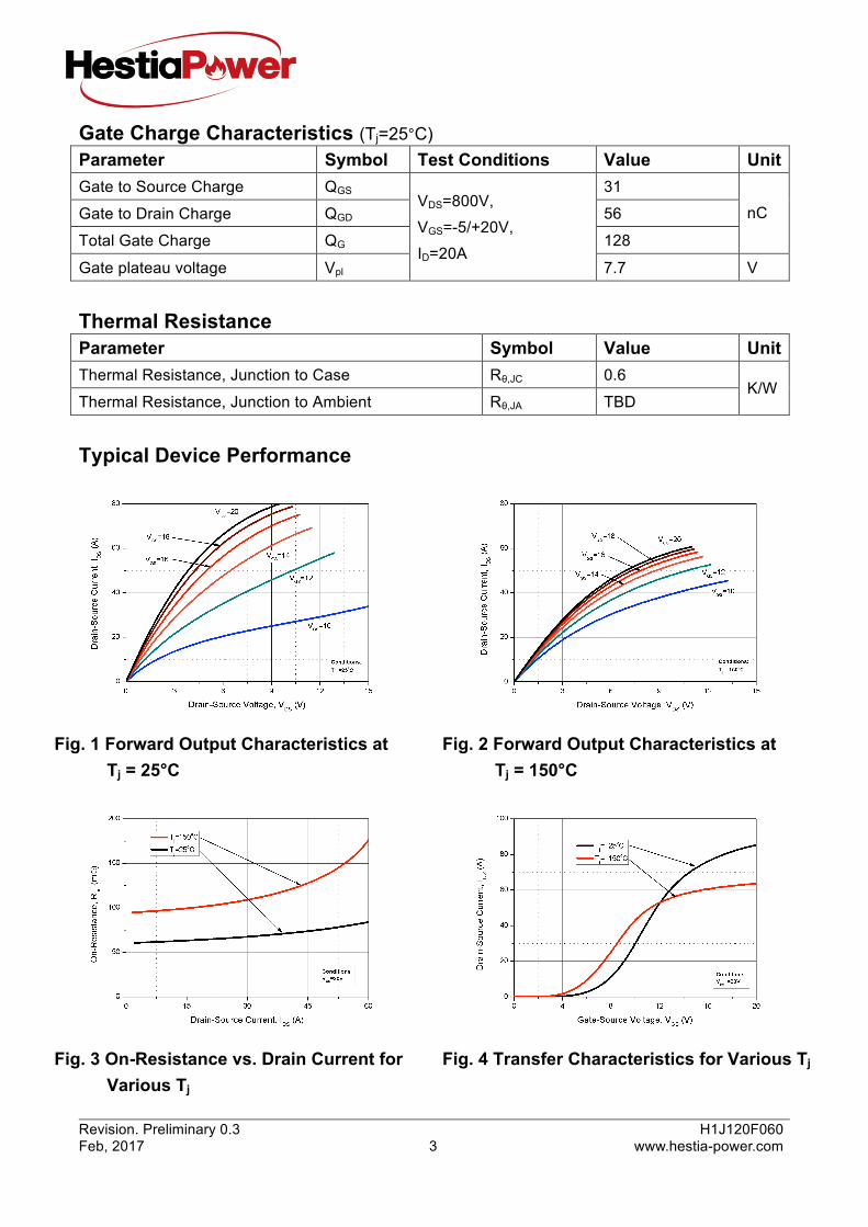
Typical Device Performance
Fig. 1 Forward Output Characteristics at Tj = 25°C
Fig. 2 Forward Output Characteristics at Tj = 150°C
Fig. 3 On-Resistance vs. Drain Current for Various Tj
Fig. 4 Transfer Characteristics for Various Tj

Revision. Preliminary 0.3 H1J120F060 Feb, 2017 4 www.hestia-power.com
Typical Device Performance
Fig. 5 On-Resistance vs. Gate Voltage for Various Tj
Fig. 6 Normalized On-Resistance vs. Temperature
Fig. 7 Reverse Output Characteristics at Tj = 25°C
Fig. 8 Reverse Output Characteristics at Tj = 150°C
Fig. 9 Capacitances vs. Drain to Source Voltage (0 - 200V)
Fig. 10 Capacitances vs. Drain to Source Voltage (0 - 1000V)

Revision. Preliminary 0.3 H1J120F060 Feb, 2017 5 www.hestia-power.com
Typical Device Performance
Fig. 11 Threshold Voltage vs. Temperature Fig. 12 Output Capacitor Stored Energy*
Fig. 13 Maximum Power Dissipation Derating vs. Case Temperature
Fig. 14 Drain Current Derating vs. Case Temperature
Fig. 15 Transient Junction to Case Thermal Impedance
Fig. 16 Safe Operating Area
Revision. Preliminary 0.3 H1J120F060 Feb, 2017 6 www.hestia-power.com
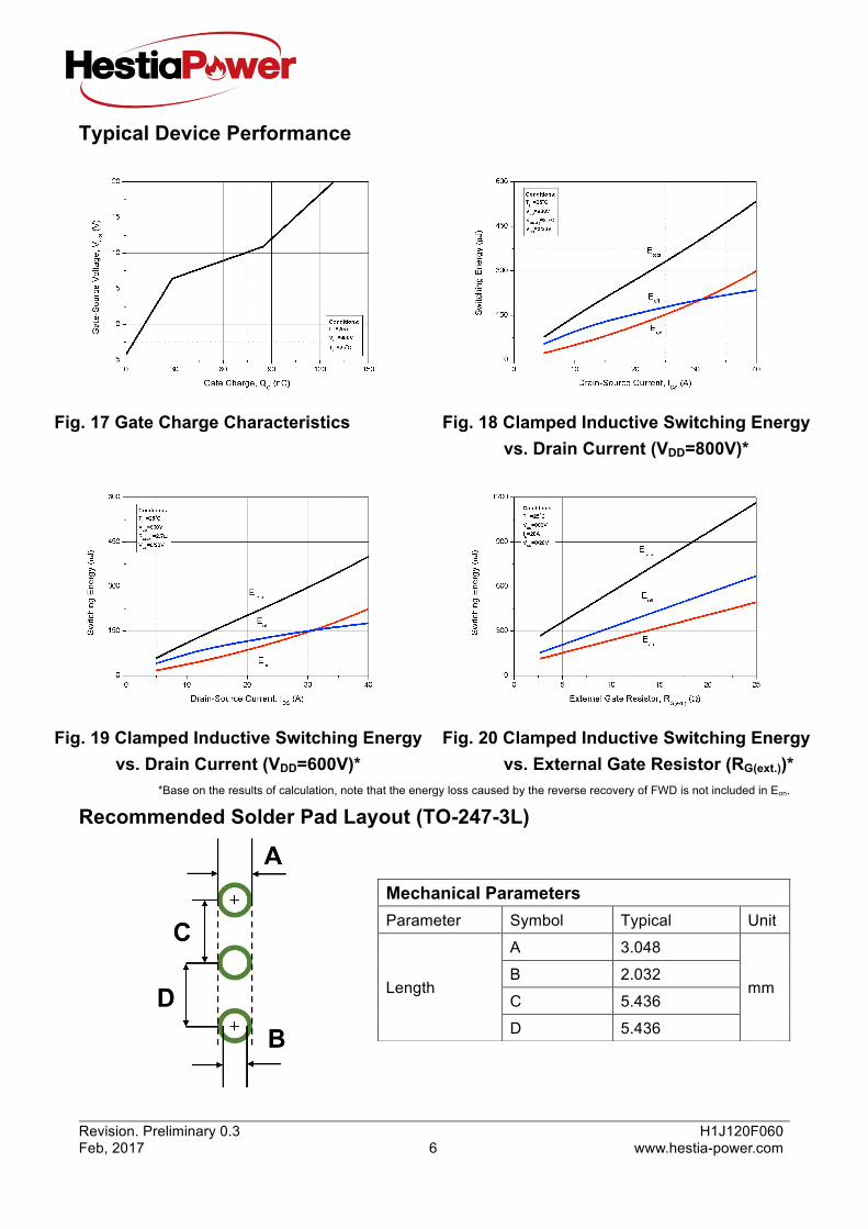
Typical Device Performance
Fig. 17 Gate Charge Characteristics Fig. 18 Clamped Inductive Switching Energy
vs. Drain Current (VDD=800V)*
Fig. 19 Clamped Inductive Switching Energy vs. Drain Current (VDD=600V)*
Fig. 20 Clamped Inductive Switching Energy vs. External Gate Resistor (RG(ext.))*
*Base on the results of calculation, note that the energy loss caused by the reverse recovery of FWD is not included in Eon.
Recommended Solder Pad Layout (TO-247-3L)
Mechanical Parameters Parameter Symbol Typical Unit
Length
A 3.048
mm B 2.032
C 5.436
D 5.436
Revision. Preliminary 0.3 H1J120F060 Feb, 2017 7 www.hestia-power.com
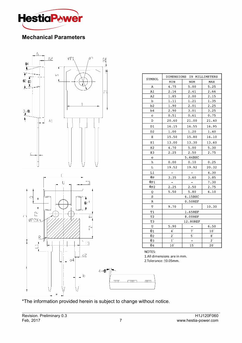
Mechanical Parameters
*The information provided herein is subject to change without notice.