Silicon Carbide power devices: Status, challenges and ... · Silicon Carbide power devices: Status,...
14
Silicon Carbide power devices: Status, challenges and future opportunities S. Reggiani, E. Gnani, A. Gnudi, G. Baccarani ARCES MODELING AND SIMULATION GROUP IUNET DAY – September 21, 2017 Advanced Research Center on Electronic Systems for Information and Communication Technologies (ARCES)
Transcript of Silicon Carbide power devices: Status, challenges and ... · Silicon Carbide power devices: Status,...

Silicon Carbide power devices: Status, challenges and future
opportunities S. Reggiani, E. Gnani, A. Gnudi, G. Baccarani
ARCES MODELING AND SIMULATION GROUP
IUNET DAY – September 21, 2017
AdvancedResearchCenteronElectronicSystemsforInformationandCommunicationTechnologies(ARCES)

Outline
q Material Advantages of SiC vs. Si q Current status of SiC Devices q What are the challenges going forward? q IUNET contributions

SiC: why? Key benefits: 3x larger bandgap, 10x larger breakdown field, 3x larger thermal conductivity
Drawbacks: • 10x device cost, • Low channel mobility (SiC/
SiO2 interface)
• Smaller size • Higher efficiency • Higher working temperature (200°C),
present limit is packaging

SiC performance à market opportunities
Channel resistance is the primary limitation to the RON in 4H-SiC MOSFETs with BV < 1kV
SiC pushes the boundary of unipolar devices for high power voltages (BV > 1kV)
SiC CAGR 2016-2020: 28% (Yole Développement, August 2017)
Cree Inc., ISPSD 2014

Main players in the SiC device industry
Company Location 2010 SiC Power Electronics Revenue (M$)
Infineon Germany 27.1 Cree USA 19.7 STMicro Italy 1.6 ROHM Japan 1.1 others 3.7
Top 4 suppliers (93% of market) Infineon and STMicroelectronics in Europe with 54% of market

Current status of SiC MOSFETs Planar MOSFETs Trench MOSFETs
ROHM, IEDM 2011
- No JFET region - Higher Mobility along the (11-20)
- Oxide reliability concerns at the trench bottom
50% lower ON resistance
Lateral MOSFET with N2O treatment
P. Fiorenza, G. Greco, F. Giannazzo, F. Iucolano, F. Roccaforte, J. Vac. Sci. Technol. B 35, 01A101 (2017)
STM, 2017

The first 1.2kV SiC MOSFET by ST The double trench by ROHM
The CoolSiC Trench MOSFET by Infineon
2015 2017
2014
fs=32 kHz, 60°C
Invited paper SiC power MOSFETs performance, robustness and technology maturity A. Castellazzi et al., Microelectronics Reliability 58 (2016)
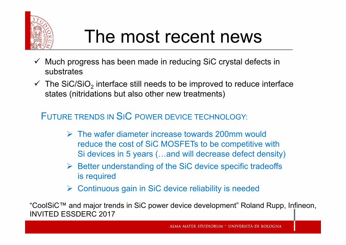
The most recent news
“CoolSiC™ and major trends in SiC power device development” Roland Rupp, Infineon, INVITED ESSDERC 2017
Ø The wafer diameter increase towards 200mm would reduce the cost of SiC MOSFETs to be competitive with Si devices in 5 years (…and will decrease defect density)
Ø Better understanding of the SiC device specific tradeoffs is required
Ø Continuous gain in SiC device reliability is needed
ü Much progress has been made in reducing SiC crystal defects in substrates
ü The SiC/SiO2 interface still needs to be improved to reduce interface states (nitridations but also other new treatments)
FUTURE TRENDS IN SIC POWER DEVICE TECHNOLOGY:

IUNET in the Project “Nano-Electronics Roadmap for Europe: Identification and Dissemination” à Task 4.2 Smart Energy (Gaudenzio Meneghesso – IUNET)
• NEREID will define the strategy for a roadmap for those technologies that extend the field of application of semiconductor technologies by adding new functionalities or extend application range.
• Smart-energy technologies, falling under the denomination of “More than Moore”, do not scale simply with geometrical size, and are widely diversified; therefore new metrics will have to be identified for the roadmap.
Roadmap and cost/benefit for WBS • Large wafer sizes, multi-wafer reactors • New circuit topologies • Novel device topologies (lateral vs vertical) • Reliability and stability of WBS
2015 ─ 2018
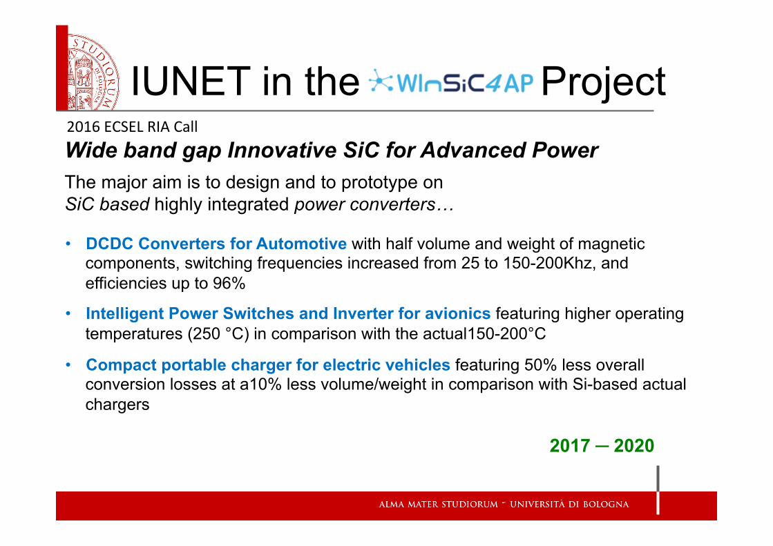
IUNET in the WinSiC Project
2016ECSELRIACallWide band gap Innovative SiC for Advanced Power
The major aim is to design and to prototype on SiC based highly integrated power converters…
2017 ─ 2020
• DCDC Converters for Automotive with half volume and weight of magnetic components, switching frequencies increased from 25 to 150-200Khz, and efficiencies up to 96%
• Intelligent Power Switches and Inverter for avionics featuring higher operating temperatures (250 °C) in comparison with the actual150-200°C
• Compact portable charger for electric vehicles featuring 50% less overall conversion losses at a10% less volume/weight in comparison with Si-based actual chargers
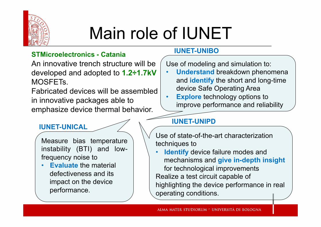
An innovative trench structure will be developed and adopted to 1.2÷1.7kV MOSFETs. Fabricated devices will be assembled in innovative packages able to emphasize device thermal behavior.
Main role of IUNET STMicroelectronics - Catania
Use of modeling and simulation to: • Understand breakdown phenomena
and identify the short and long-time device Safe Operating Area
• Explore technology options to improve performance and reliability
IUNET-UNIBO
IUNET-UNICAL IUNET-UNIPD
Use of state-of-the-art characterization techniques to • Identify device failure modes and
mechanisms and give in-depth insight for technological improvements
Realize a test circuit capable of highlighting the device performance in real operating conditions.
Measure bias temperature instability (BTI) and low-frequency noise to • Evaluate the material
defectiveness and its impact on the device performance.

IUNET in the REACTION Proposal
2017ECSELIACallFirst and European SiC Eigth Inches Pilot line
• REACTION will push through the first worldwide 200mm Silicon Carbide (SiC) Pilot Line Facility for Power technology.
• The 200mm SiC Pilot Line will be located in the ST wafer fab of Catania (Italy), and it will share facilities with the current 6’’ line.

• Performance evaluation and understanding of threshold voltage drift during bias temperature instability (BTI) stress;
• Evaluation of device stability in switching-mode and comparison of DUTs fabricated with different process options;
• Ab-initio simulations of defects and traps to identify energy, type of traps and activation mechanisms;
• TCAD simulations of Power SiC devices aimed at the device structure optimization and accounting for the degradation effects;
• Identification of device failure modes and mechanisms for the development of a Robust and reliable Power SiC devices.
Main role of IUNET
IUNET-UNIBO
IUNET-UNICAL
IUNET-UNIPI
IUNET-UNIMORE
IUNET-UNIPD