Grace Xing---EE30357 (Semiconductors II: Devices) 1 EE 30357: Semiconductors II: Devices Lecture...
13
Grace Xing---EE30357 (Semiconductors II: Devices) 1 EE 30357: Semiconductors II: Devices Lecture Note #19 (02/27/09) MOS Field Effect Transistors Grace Xing Outline: 1. Last class: Small signal equivalent circuit model & Short channel effects 2. Compound semiconductor based devices 1. MESFET 2. JFET 3. HEMT 3. Quick revisit of MOS capacitors and FETs (read on your own how DRAM, CCD, flash memory etc. work, they are all based on MOS structures!) – next class 1. Flat band voltage 2. Effects of oxide charges (interface charges, fixed charges)
-
Upload
rachel-lang -
Category
Documents
-
view
220 -
download
0
Transcript of Grace Xing---EE30357 (Semiconductors II: Devices) 1 EE 30357: Semiconductors II: Devices Lecture...

Grace Xing---EE30357 (Semiconductors II: Devices) 1
EE 30357: Semiconductors II: DevicesLecture Note #19 (02/27/09)
MOS Field Effect Transistors Grace Xing
Outline:
1. Last class: Small signal equivalent circuit model & Short channel effects
2. Compound semiconductor based devices1. MESFET2. JFET3. HEMT
3. Quick revisit of MOS capacitors and FETs (read on your own how DRAM, CCD, flash memory etc. work, they are all based on MOS structures!) – next class
1. Flat band voltage2. Effects of oxide charges (interface charges, fixed charges)

Grace Xing---EE30357 (Semiconductors II: Devices) 2
Schematic showing the structure of a GaAs MESFET.
Figure 8.26

Grace Xing---EE30357 (Semiconductors II: Devices) 3
(a) Cross section of a MESFET at equilibrium indicating the depletion regions; (b) the energy band diagram
perpendicular to the gate. The channel thickness is t.
Figure 8.27
metal
SiO2 SiO2
Si
Similar to the SOI devices (ultra-scaled MOSFET), electrons are confined in the channel by large bandgap materials
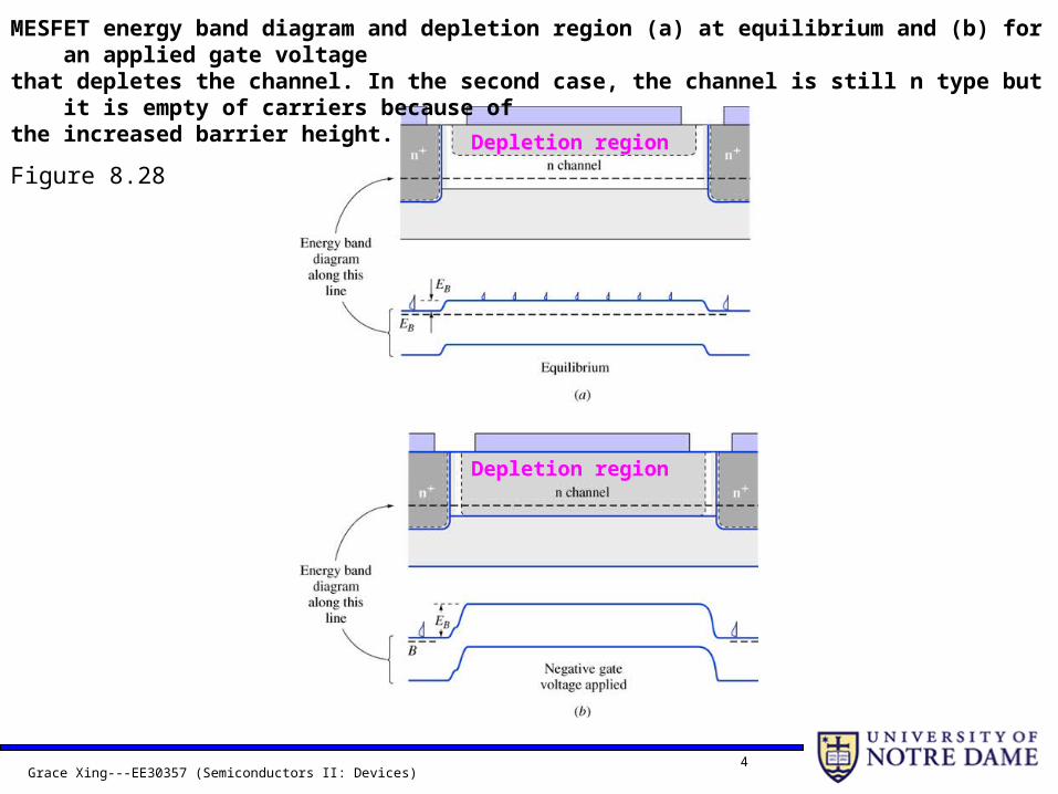
Grace Xing---EE30357 (Semiconductors II: Devices) 4
MESFET energy band diagram and depletion region (a) at equilibrium and (b) for an applied gate voltage
that depletes the channel. In the second case, the channel is still n type but it is empty of carriers because of
the increased barrier height.
Figure 8.28
Depletion region
Depletion region

Grace Xing---EE30357 (Semiconductors II: Devices) 5
Cross section of a MESFET under small VDS bias and the corresponding energy band diagrams at the source
end and drain end of the gate.
Figure 8.29
1 V
1 eV
Mistakes in textbook(There are quite some mistakes on MESFET and HEMTs in Anderson. Use my slides instead.)

Grace Xing---EE30357 (Semiconductors II: Devices) 6
The JFET. The shaded areas represent the depletion regions. (a) Cross-sectional diagram; (b) the energy band
diagram, (EC), for VDS = 0; (c) when VDS 0 (but not yet in saturation) the depletion region at the drain end
increases, narrowing the channel and increasing the channel resistance.
Figure 8.32
Substrate
gate

Grace Xing---EE30357 (Semiconductors II: Devices) 7

Grace Xing---EE30357 (Semiconductors II: Devices) 8

Grace Xing---EE30357 (Semiconductors II: Devices) 9
Gradual channel approximation• Channel is long such that electric field L << T
• Gate depletion w is independent of L(y)

Grace Xing---EE30357 (Semiconductors II: Devices) 10
• Gradual channel approximation• n(y) ~ ND’• long channel and constant low-field mobility lf
• No need to remember these equations
'
1/ 2
'
1/ 2
'
1/ 2
'
( )1
2( ) ( ( ))
( ( ))
, (0) , 0
2(0) ( )
( )1
D lf D ch
sbi GS ch
D
j bi GS ch
ch
sbi T
D
bi GS chD lf D
bi T
w yI dy qW N a dV
a
w y V V V yqN
whereV V V V y
At threshold w a V
w a V VqN
V V V yI dy qW N a
V V
'
3 / 2 3/ 2
2( )
3
ch
lf DD
DS bi GS bi GSDS bi T
bi T bi T
dV
current can be solved in sublinear regionqW N a
IL
V V V V VV V V
V V V V

Grace Xing---EE30357 (Semiconductors II: Devices) 11
High electron mobility transistor (HEMT)(other names are Modulation Doped FET – MODFET and
Heterojunction FET - HFET)
Mobile electrons are separated from the ionized donors less scattering high mobility!
Error in A&A, Fig.8.24 (b) and description of how gate works are wrong.The other parts are reasonably correct.

Grace Xing---EE30357 (Semiconductors II: Devices) 12

Grace Xing---EE30357 (Semiconductors II: Devices) 13
High speed IC – NTT 80 Gbits/s multiplexer
HEMTs can operate much faster than MOSFETs
high speed ICs