GPS pcb design 1v0 - Fujitsu · The 1.2V regulator would be enabled when GPS functionality is...
28
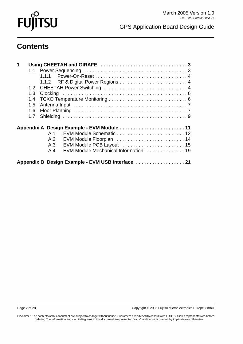
Copyright © 2005 Fujitsu Microelectronics Europe GmbH Page 1 of 28 Disclaimer: The contents of this document are subject to change without notice. Customers are advised to consult with FUJITSU sales representatives before ordering.The information and circuit diagrams in this document are presented “as is”, no license is granted by implication or otherwise. Design Guide March 2005 Version 1.0 FME/MS/GPS/DG/5192 GPS Application Board Design Guide Mixed Signal Division This document helps guide the user through designing an application board for the Fujitsu GPS/AGPS receiver chipset. Detailed application circuits are given for the RF and baseband devices, along with suggestions for external component selection. PCB design guidelines are also included. Designs for both a compact GPS receiver (EVM) module, and a USB interface board for this module are given as example layouts. Throughout this document the RF Front End (MB15H156) is referred to as GIRAFE, and the baseband device (MB87Q2040) is referred to as CHEETAH. This document should be read in conjunction with the datasheets for both GIRAFE and CHEETAH, and the application note “GPS/AGPS Design Example And Layout”. Features • Detailed application circuit design guidelines • Component selection guidelines • Ready-to-manufacture GPS receiver module PCB design • Adaptable USB Interface design example GPS Module EVM USB Interface
Transcript of GPS pcb design 1v0 - Fujitsu · The 1.2V regulator would be enabled when GPS functionality is...
Design Guide
March 2005Version 1.0
FME/MS/GPS/DG/5192
GPS Application Board Design Guide
Mixed Signal Division
This document helps guide the user through designing an
application board for the Fujitsu GPS/AGPS receiver chipset.
Detailed application circuits are given for the RF and baseband
devices, along with suggestions for external component
selection. PCB design guidelines are also included.
Designs for both a compact GPS receiver (EVM) module, and
a USB interface board for this module are given as example
layouts.
Throughout this document the RF Front End (MB15H156) is
referred to as GIRAFE, and the baseband device
(MB87Q2040) is referred to as CHEETAH.
This document should be read in conjunction with thedatasheets for both GIRAFE and CHEETAH, and theapplication note “GPS/AGPS Design Example And Layout”.
Features• Detailed application circuit design guidelines• Component selection guidelines• Ready-to-manufacture GPS receiver module PCB design• Adaptable USB Interface design example
GPS Module
EVM USB Interface
Copyright © 2005 Fujitsu Microelectronics Europe GmbH Page 1 of 28
Disclaimer: The contents of this document are subject to change without notice. Customers are advised to consult with FUJITSU sales representatives before ordering.The information and circuit diagrams in this document are presented “as is”, no license is granted by implication or otherwise.
March 2005 Version 1.0FME/MS/GPS/DG/5192
GPS Application Board Design Guide
Contents
1 Using CHEETAH and GIRAFE . . . . . . . . . . . . . . . . . . . . . . . . . . . . . . . . 31.1 Power Sequencing . . . . . . . . . . . . . . . . . . . . . . . . . . . . . . . . . . . . . . 3
1.1.1 Power-On-Reset . . . . . . . . . . . . . . . . . . . . . . . . . . . . . . . . . . 41.1.2 RF & Digital Power Regions . . . . . . . . . . . . . . . . . . . . . . . . . 4
1.2 CHEETAH Power Switching . . . . . . . . . . . . . . . . . . . . . . . . . . . . . . . 41.3 Clocking . . . . . . . . . . . . . . . . . . . . . . . . . . . . . . . . . . . . . . . . . . . . . . 61.4 TCXO Temperature Monitoring . . . . . . . . . . . . . . . . . . . . . . . . . . . . . 61.5 Antenna Input . . . . . . . . . . . . . . . . . . . . . . . . . . . . . . . . . . . . . . . . . . 71.6 Floor Planning . . . . . . . . . . . . . . . . . . . . . . . . . . . . . . . . . . . . . . . . . . 71.7 Shielding . . . . . . . . . . . . . . . . . . . . . . . . . . . . . . . . . . . . . . . . . . . . . . 9
Appendix A Design Example - EVM Module . . . . . . . . . . . . . . . . . . . . . . . . 11A.1 EVM Module Schematic . . . . . . . . . . . . . . . . . . . . . . . . . 12A.2 EVM Module Floorplan . . . . . . . . . . . . . . . . . . . . . . . . . 14A.3 EVM Module PCB Layout . . . . . . . . . . . . . . . . . . . . . . . 15A.4 EVM Module Mechanical Information . . . . . . . . . . . . . . 19
Appendix B Design Example - EVM USB Interface . . . . . . . . . . . . . . . . . . 21
Page 2 of 28 Copyright © 2005 Fujitsu Microelectronics Europe GmbH
Disclaimer: The contents of this document are subject to change without notice. Customers are advised to consult with FUJITSU sales representatives before ordering.The information and circuit diagrams in this document are presented “as is”, no license is granted by implication or otherwise.

March 2005 Version 1.0FME/MS/GPS/DG/5192
GPS Application Board Design Guide
1 Using CHEETAH and GIRAFE
1.1 Power SequencingThe 1.2V and 3.3V power supplies to CHEETAH and the 3.3V supply to GIRAFE must be sequencedcorrectly to ensure that CHEETAH starts-up and shuts-down cleanly.
The 1.2V rail is only used to supply the core logic of CHEETAH, and must be applied first. Once thissupply is stable, the 3.3V supply for the I/O of CHEETAH and all of GIRAFE may be applied.
Figure 1 Power Sequencing
During power-up care should be taken to ensure that there are no CHEETAH I/O pads pulled up to3.3V by another device that is already powered. If this is the case, then the VDDE supply region ofCHEETAH may be powered through the I/O cell. The result of this would be to break the powersequencing rules for CHEETAH, resulting in the device failing to start-up correctly.
Figure 2 Using Voltage Regulators for Power Sequencing
An easy way to achieve this power sequencing is to utilise the ‘Enable’ and ‘Power-Good’ functionbuilt into many voltage regulators. The 1.2V regulator would be enabled when GPS functionality isrequired. Once the output of the 1.2V regulator has reached regulation the ‘Power-Good’ output
CHEETAH 1.2V
GIRAFE 3.3VCHEETAH 3.3V
1.2V 3.3V
1.2V supply 3.3V supply
Battery
GPS Enable
Ena
ble
Regulator RegulatorEna
ble
Pow
er G
ood
Pow
er G
ood
GPS Reset
Copyright © 2005 Fujitsu Microelectronics Europe GmbH Page 3 of 28
Disclaimer: The contents of this document are subject to change without notice. Customers are advised to consult with FUJITSU sales representatives before ordering.The information and circuit diagrams in this document are presented “as is”, no license is granted by implication or otherwise.
March 2005 Version 1.0FME/MS/GPS/DG/5192
GPS Application Board Design Guide
would be used to enable the 3.3V regulator. This ensureS that the 1.2V supply is always appliedbefore the 3.3V supply. See Appendix B for an example application circuit using two linear regulators(Note - this application circuit is suitable for 5V input supply applications only).
1.1.1 Power-On-ResetIn addition to providing the power supply sequencing for CHEETAH, voltage regulators with power-good outputs can be used to provide a power-on-reset signal for CHEETAH. The power-good outputfrom the 3.3V regulator can be connected to the reset pin (NRST). Only once both the 1.2V and 3.3Vsupplies are in regulation would the reset signal be removed. This would ensure that CHEETAHwould start-up cleanly at initial power-up, and would be reset during brown-out conditions.
1.1.2 RF & Digital Power RegionsA single regulator can be used to provide a 3.3V supply for both CHEETAH and GIRAFE. However,care should be taken to ensure that digital noise from CHEETAH does not get onto the supply for thesensitive RF region that includes GIRAFE and the TCXO. An inductor (intended for power supplyfiltering, not a high-Q RF inductor) should be used to filter the 3.3V supply between the digital andRF region.
1.2 CHEETAH Power SwitchingCHEETAH has the ability to power-down a section of itself to minimise the power consumption whennot tracking (there are a number of power saving modes, each controlled by the client code on thehost processor. See the CHEETAH datasheet for more details). This is done with external FETscontrolled by the non-switched region of CHEETAH. One N-channel and two P-channel MOSFETsare required to switch the 1.2V and 3.3V supplies to the VDDI2 and VDDE2/3 regions.
The N-channel FET is used to switch the 1.2V supply. This FET is controlled by the VIPFET pin ofCHEETAH, and should be selected to have a RON value typically <0.5Ω at VGS = 1.8V. One of theP-channel FETs is used to switch the 3.3V supply. This FET is controlled by the VINFET pin ofCHEETAH, and should be selected to have a RON value of <5Ω at VGS = 3.3V.
A suitable dual P and N-channel MOSFET is available from Vishay Siliconix (www.vishay.com), partnumber Si1563EDH. The P-channel FET in this device has a lower RON value than required, butwhen considering the total package size and cost of this dual FET device, it provides a better solutionthan two discrete FETs.
The gate series resistor values for both of the FETs should be chosen to allow the FETs to switch theVDDI2 region on before the VDDE2/3 region, thus ensuring the correct power supply sequence forthe switched region of CHEETAH. Typically, the P-channel FET series resistor will be larger than theN-channel FET series resistor. If using the Si1563EDH and a similar application circuit to that shownin Appendix A, then the P-channel gate resistor should be 68kΩ, and the N-channel gate resistorshould be 22kΩ.
Page 4 of 28 Copyright © 2005 Fujitsu Microelectronics Europe GmbH
Disclaimer: The contents of this document are subject to change without notice. Customers are advised to consult with FUJITSU sales representatives before ordering.The information and circuit diagrams in this document are presented “as is”, no license is granted by implication or otherwise.
March 2005 Version 1.0FME/MS/GPS/DG/5192
GPS Application Board Design Guide
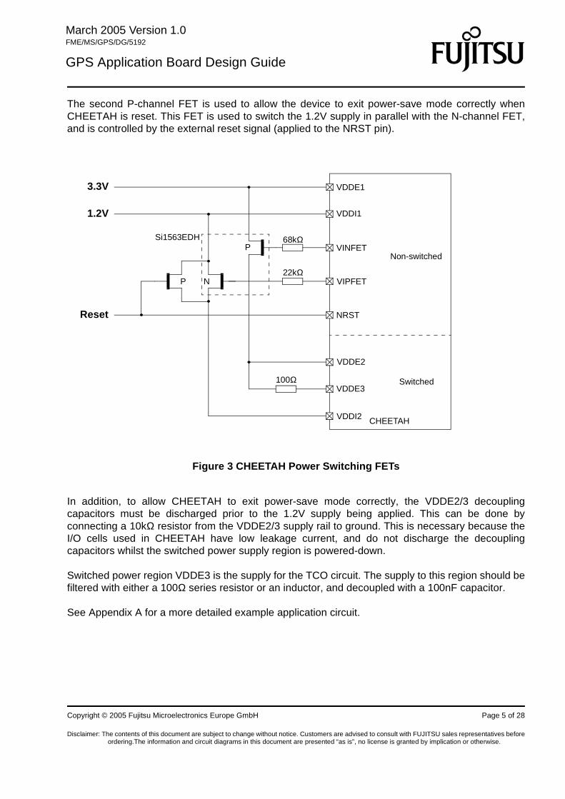
The second P-channel FET is used to allow the device to exit power-save mode correctly whenCHEETAH is reset. This FET is used to switch the 1.2V supply in parallel with the N-channel FET,and is controlled by the external reset signal (applied to the NRST pin).
Figure 3 CHEETAH Power Switching FETs
In addition, to allow CHEETAH to exit power-save mode correctly, the VDDE2/3 decouplingcapacitors must be discharged prior to the 1.2V supply being applied. This can be done byconnecting a 10kΩ resistor from the VDDE2/3 supply rail to ground. This is necessary because theI/O cells used in CHEETAH have low leakage current, and do not discharge the decouplingcapacitors whilst the switched power supply region is powered-down.
Switched power region VDDE3 is the supply for the TCO circuit. The supply to this region should befiltered with either a 100Ω series resistor or an inductor, and decoupled with a 100nF capacitor.
See Appendix A for a more detailed example application circuit.
1.2V
3.3V VDDE1
VDDI1
VDDE2
VDDE3
VDDI2
Reset
VINFET
NRST
VIPFET
68kΩ
22kΩ
100Ω
Si1563EDHP
NP
Switched
Non-switched
CHEETAH
Copyright © 2005 Fujitsu Microelectronics Europe GmbH Page 5 of 28
Disclaimer: The contents of this document are subject to change without notice. Customers are advised to consult with FUJITSU sales representatives before ordering.The information and circuit diagrams in this document are presented “as is”, no license is granted by implication or otherwise.

March 2005 Version 1.0FME/MS/GPS/DG/5192
GPS Application Board Design Guide
1.3 ClockingA 27.456MHz clock source is required by GIRAFE and CHEETAH. This clock source is best providedby a TCXO. The recommended TCXO is from RAKON (www.rakon.com), part number IT3205BE -TX3788. This is in an ultra-small 3.2 x 2.5mm package.
The output from the TCXO should be AC coupled with a 47pF capacitor, and applied to the REFinpin of GIRAFE. This clock signal is buffered in GIRAFE, and is available for connection to CHEETAHon pin CLKout. Connect this pin to CHEETAH with 100pF AC coupling capacitor. The TCXO shouldbe powered from the same 3.3V supply as GIRAFE.
Figure 4 GIRAFE and CHEETAH Clocking
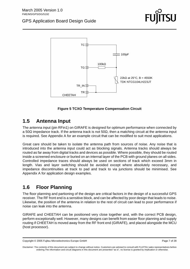
1.4 TCXO Temperature MonitoringThe temperature of the TCXO is monitored by the software to compensate for any offset and non-linearity in the frequency of the TCXO versus temperature. To do this a thermistor should be includedin an RC oscillator circuit connected to CHEETAH.
The recommended thermistor is available from TDK (www.tdk-components.de) part numberNTCG104LH223JT. This is a 22kΩ (at 25°C) thermistor, with a B constant of 4550K (at 25/85°C).
To measure the temperature of the TCXO, the thermistor should be positioned as close to the TCXOpackage as possible. If positioned close enough, the thermistor will track the TCXO temperature byheat conduction through the PCB substrate.
CHEETAHGIRAFE
TCXO
REFin
CLKout MCLKI
47pF
100pF
3.3V (RF) 3.3V (Digital)
F out
GND
Page 6 of 28 Copyright © 2005 Fujitsu Microelectronics Europe GmbH
Disclaimer: The contents of this document are subject to change without notice. Customers are advised to consult with FUJITSU sales representatives before ordering.The information and circuit diagrams in this document are presented “as is”, no license is granted by implication or otherwise.
March 2005 Version 1.0FME/MS/GPS/DG/5192
GPS Application Board Design Guide
Figure 5 TCXO Temperature Compensation Circuit
1.5 Antenna InputThe antenna input (pin RFin1) on GIRAFE is designed for optimum performance when connected bya 50Ω impedance track. If the antenna track is not 50Ω, then a matching circuit at the antenna inputis required. See Appendix A for an example circuit that can be modified to suit most applications.
Great care should be taken to isolate the antenna path from sources of noise. Any noise that isintroduced into the antenna input could act as blocking signals. Antenna tracks should always berouted as far away from digital tracks and devices as possible. Where possible, they should be routedinside a screened enclosure or buried on an internal layer of the PCB with ground planes on all sides.Controlled impedance traces should always be used on sections of track which exceed 3mm inlength. Vias and layer switching should be avoided except where absolutely necessary, andimpedance discontinuities at track to pad and track to via junctions should be minimised. SeeAppendix A for application design examples.
1.6 Floor PlanningThe floor planning and partioning of the design are critical factors in the design of a successful GPSreceiver. The RF front end is a sensitive block, and can be affected by poor design that leads to noise.Likewise, the position of the antenna in relation to the rest of circuit can lead to poor performance ifnoise can leak into the antenna.
GIRAFE and CHEETAH can be positioned very close together and, with the correct PCB design,perform exceptionally well. However, many designs can benefit from easier floor planning and supplyrouting if CHEETAH is moved away from the RF front end (GIRAFE), and placed alongside the MCU(host processor).
TC
TG
TR_IN
TRCHEETAH
100kΩ
100pF
22kΩ at 25°C, B = 4550KTDK NTCG104LH223JT
Copyright © 2005 Fujitsu Microelectronics Europe GmbH Page 7 of 28
Disclaimer: The contents of this document are subject to change without notice. Customers are advised to consult with FUJITSU sales representatives before ordering.The information and circuit diagrams in this document are presented “as is”, no license is granted by implication or otherwise.

March 2005 Version 1.0FME/MS/GPS/DG/5192
GPS Application Board Design Guide
A typical design that can benefit from this approach is the portable “Bluetooth” receiver, that willusually have the antenna integrated into the device. In this case, the floor planning of the board istotally driven by the need to isolate the antenna from all sources of noise, whilst minimising theseparation between the antenna and the RF front end.
The patch antennas typically used in such devices require a large ground plane below them toachieve the stated gain. Although this ground plane is limiting in that it prevents the mounting of anycomponents on the top of the board, it does provide an excellent shield that prevents noise from theopposite side of the board from being picked up by the antenna. This now constrains the floor planto locating the RF front end and the MCU on the same side of the board. GIRAFE could be positioneddirectly below the patch antenna, so keeping the antenna input path as short as possible. Then,CHEETAH and the MCU could be positioned as a separate block at the far end of the board,providing a reasonable separation between the noisy digital circuits and the sensitive RF front end.See Figure 6. The maximum track length between GIRAFE and CHEETAH is governed by themaximum capacitive load seen by each I/O pin. The maximum is 15pF, so assuming 5pF for the I/Ocapacitance of the packages at both ends, the track should be designed to contribute no more than10pF (based on the application board layer stack, material and track width).
Figure 6 Separating GIRAFE and CHEETAH in a typical “Bluetooth” Receiver
A partial split can be introduced into the ground planes between the RF and digital regions. All signaland power tracks between the two regions must pass across the bridge between the RF and digitalground plane areas so that the ground return currents can follow the signal path. Signal and powertracks must never cross a ground plane split.
The TCXO must be positioned in the RF region next to GIRAFE to minimise clock jitter. However, thethermistor that measures the temperature of the TCXO is connected to CHEETAH and must bepositioned close to the TCXO. This means that the potentially noisy TCO tracks to the thermistormust cross from the digital region into the RF region. To prevent these tracks radiating noise, stepsmust be taken to screen them from the sensitive RF input and antenna tracks. A suitable means todo this is to route these tracks on an internal layer, shielded from both the antenna tracks and thepatch antenna by a ground plane.
TCXO
GIRAFECHEETAH
MCU /Patch antenna(on reverse side)
Gro
und
plan
e sp
lit
Bluetooth
Page 8 of 28 Copyright © 2005 Fujitsu Microelectronics Europe GmbH
Disclaimer: The contents of this document are subject to change without notice. Customers are advised to consult with FUJITSU sales representatives before ordering.The information and circuit diagrams in this document are presented “as is”, no license is granted by implication or otherwise.
March 2005 Version 1.0FME/MS/GPS/DG/5192
GPS Application Board Design Guide
Likewise, the sign and magnitude signals, and the GIRAFE to CHEETAH clock signal must crossfrom the RF region to the digital region. These signals should be routed on an internal layer shieldedby a ground plane also. The GIRAFE ClkEN and ChipEN signals are static signals, so shielding isnot as important. The digital I/O cells on both GIRAFE and CHEETAH were designed to provide aweaker than normal drive level, so limiting the noise generation by reducing slew rates.
The overall aim should be to design every part of the floor plan with noise minimisation andcontainment in mind.
1.7 ShieldingThe performance of all GPS receivers is influenced significantly by the presence of noise. This noisecan act as blocking signals that prevents the receiver from obtaining a position fix. In many cases theworst culprit for noise emission is the receiver itself, especially noticable when the receiver has aninternal antenna.
All receiver designs should incorporate some form of shielding. The emphasis should be placed onthe containment of noise generated by both the digital circuits in the receiver, and the interconnectionmethod to the outside world. Assuming that the floor plan has been designed correctly for minimalnoise emission, then effort should be directed at containing the un-avoidable noise emission.
Considering the “Bluetooth” receiver example floor plan shown in Figure 6, two shielding cans wouldbe necessary. One screening can should be fitted to the board over the RF region, shielding thesensitive antenna input from radiated noise, and stopping emission of noise from the TCXO and theTCO circuit around the thermistor. A second shielding can would be fitted over the digital region, sopreventing the significant noise emission from here. This shielding can should also extend over theregulators and the interface device (Bluetooth, RS-232, USB etc). Now, as the top side of the boardis covered by a ground plane for the patch antenna, and that all components are covered by theshielding cans, there should be no path for noise emissions to escape the receiver and jam the GPSsignal.
For designs that use a remote external antenna, the shielding requirements are less stringent. In thiscase, it may only be necessary to shield the RF section to prevent noise pick-up into the antennainput. Emissions from the digital section are only of concern if the antenna is positioned within closeproximity of the digital noise sources.
Special attention should be paid to the connection method of wired interfaces such as RS-232 andUSB. Significant noise can be emitted if poor connection methods are used in the termination of thesecables. Where shielded cables are used, the connection from the shield to the board should be a verylow inductance path, and the shield mechanism should be extended to cover the signal (and powerfor USB) connections. USB connectors are typically much better than D-type connectors for this.
One example of where poor shielding of cables can impact on performance is in the “GPS Mouse”type of receiver. Here, the interface cable is typically hard-wired into the device, and an internal patchantenna is used. The usual method to connect the USB connection cable is to strip the outer sheathand shielding braid back by around 20mm, and to make a “pig-tail” of the shield. The shield, powerand signal wires are then either crimped into a header, or soldered directly onto pads on the board.The result is that the cable shield is connected to the board with a 20mm long cable that has
Copyright © 2005 Fujitsu Microelectronics Europe GmbH Page 9 of 28
Disclaimer: The contents of this document are subject to change without notice. Customers are advised to consult with FUJITSU sales representatives before ordering.The information and circuit diagrams in this document are presented “as is”, no license is granted by implication or otherwise.

March 2005 Version 1.0FME/MS/GPS/DG/5192
GPS Application Board Design Guide
significant inductance. This will now cause noise to be radiated by the cable shield because it is notgrounded well at RF frequencies.
Figure 7 Example USB Cable PCB Termination Methods
To minimise this, the connection between the receivers ground plane and the cable shield shouldhave as low an inductance as possible. Using the same cable, the shield can be split into two “pig-tails”, both of which should be shortened to the minimum length possible, and soldered directly to anexposed ground plane area.
The best termination method would be to use crimp-on shielded cable terminators (intended for co-axial cable termination) that provide a 360° termination of the shielding braid, and connect to theboards ground plane with multiple pins. See Figure 8. The signal and power wires would then beterminated as before, but should be kept as short as possible. If space permits, the overall cabletermination area should be screened with a shielding can.
Suitable shielded cable terminators are available from Johnson Components(www.johnsoncomponents.com).
Figure 8 Shielded Cable Terminator
High inductance shield ‘pig-tail’
Long un-shielded powerand signal wires
!
Shorter un-shielded power
"
Dual low inductance
and signal wires
shield ‘pig-tails’
Page 10 of 28 Copyright © 2005 Fujitsu Microelectronics Europe GmbH
Disclaimer: The contents of this document are subject to change without notice. Customers are advised to consult with FUJITSU sales representatives before ordering.The information and circuit diagrams in this document are presented “as is”, no license is granted by implication or otherwise.

March 2005 Version 1.0FME/MS/GPS/DG/5192
GPS Application Board Design Guide
Appendix A Design Example - EVM Module
This section details the design of a 13 x 18.5mm module that contains an entire application circuit forGIRAFE and CHEETAH.
The EVM module consists of GIRAFE, CHEETAH, TCXO, SAW filter, both power switching FETs,and all passive components required to provide a fully functional GPS receiver front-end.
The board is manufactured on a conventional 4-layer FR-4 process. The finished PCB thickness is1mm, and the smallest drill size is 0.2mm, making the board suitable for low-cost manufacturing lines.All passive components are either 0402 or 0603 size.
The positioning of the connection points at either end of the board was chosen to minimise noisecoupling from the digital signals at one end, to the sensitive RF input at the other end. This helps boththe EVM module and the motherboard that it will be mounted on. Maximum isolation between thenoisy UART interface and the antenna input has been achieved through careful floor-planning of theboard design, keeping tracking to the Tx and Rx pins to a minimum, and keeping them away from theRF end of the board. This, along with consideration of the location of all critical components in relationto the device I/O pins, results in a high performance and compact design.
Copyright © 2005 Fujitsu Microelectronics Europe GmbH Page 11 of 28
Disclaimer: The contents of this document are subject to change without notice. Customers are advised to consult with FUJITSU sales representatives before ordering.The information and circuit diagrams in this document are presented “as is”, no license is granted by implication or otherwise.

March 2005 Version 1.0FME/MS/GPS/DG/5192
GPS Application Board Design Guide
Appendix A.1 EVM Module Schematic
Figure A1 EVM Module Schematic
12
34
56
ABCD
65
43
21
D C B A
Titl
e
Num
ber
Rev
isio
nS
ize
B
Dat
e:28
-Feb
-200
5S
heet
o
f
File
:R
:\PC
B-d
esig
ns\..
\EV
M_M
odule_
1v3_p
ublis
h.S
chD
raw
n By:
NRST1
RX2
VDDI13
VINFET4
VDDE15
VIPFET6
VDDI27
TC8
TR_IN9
VDDE310
TR11
TG12
TS
TS
EL0
13TM
S14
TR
ST
15TD
I16
TC
K17
VD
DI2
18V
DD
E2
19TD
O20
TX
21S
PR
322
PPS
23S
PR
224
MSEC25
SPR126
MSEC1027
TSTSEL228
MSECI29
VDDI230
VDDE231
FRQCK32
EPPS33
TSTSEL134
IM35
IS36
AG
C1
37
AG
C4
38
VPD
39
VD
DE2
40
QM
41
QS
42
VD
DI2
43
VD
DI1
44
MC
LKO
SC
45
MC
LKI
46
VD
DE1
47
EN
RF
48
U2A
CH
EE
TA
H
GND49
U2B
CH
EE
TA
H
RT1
22k
@ 2
5degC
534
P
T1B
SI1
563E
DH
FE
T
16
2
N
T1A
SI1
563E
DH
FE
T
C32
100nF
C33
100nF
C31
100nF
C30
100nF
C28
100nF
C29
100nF
C27
100nF
C26
100nF
C25
100nF
C24
100nF
GN
DG
ND
GN
DG
ND
GN
DG
ND
GN
DG
ND
3V3_
1
3V3_
1
3V3_
2
3V3_
2
3V3_
2
3V3_
2
1V2_
1
1V2_
1
1V2_
2
1V2_
2
1V2_
2
1V2_
2
GN
DG
ND
R9
100k
C38
100pF
C21
100pF
C36
1uF 1
0V
C37
1uF 1
0V G
ND
GN
D3V3_
1
1V2_
11V
2_2
3V3_
2
TP
9A
NT
TP
10
GN
D
TP
13
3V
3
TP
12
1V
2
TP
16
GN
D
TP
15
TX
D
TP
14
RX
D
TP
6R
ST
GN
D
(C) 20
05 F
ujits
u M
icro
elec
tron
ics
Eur
ope
Gm
bH - G
PS
Eva
luat
ion
(EV
M) M
odul
e sc
hem
atic V
ersi
on 1
v3
GN
D
GN
D
GN
D
GN
D
C8
10nF
C4
1n
C35
100nF
C5
1n
C1
1n
C7
10nF
C11
10nF
C3
100n
C2
1n
C10
100nF
GN
D
GN
D
C13
100p
R2
10k
GN
D
GN
D
GN
DG
ND
GN
D
GN
D
GN
D
VC
C4
GN
D1
GN
D2
OU
T3
U3
TO
YO
CO
M T
CO
-5879
GN
D
C20
47pF
R5
15k
C34
1nF
GN
D
GN
DR
F1
GN
DR
F2
RFou
t13
GN
DLN
A4
RFin
15
LNA
E6
VC
CLN
A7
NC
8
CLKout9
VCCD10
VCOREG11
GNDvco12
RefR13
MODE14
ClkEN15
ChipEN16
REFin
17
REFou
t18
GN
DD
19
AO
UT
20
VC
CA
GC
21
IM22
IS23
GN
DIF
24
PWM25
VCCIF26
AGCEN27
GNDIF28
VTUNE29
GNDRF30
VCCRF31
RFin232
U1
GIR
AFE
C19
N/F
L1
0R
0
GN
D
C17
100pF
GN
D
C18
N/F
3V3_
RF
3V3_
RF
3V3_
RF
3V3_
RF
3V3_
RF
TP
33V
3_R
F
3V3_
RF
3V3_
RF
GN
D4
IN1
OU
T3
GN
D2
X1
FA
R-F
6E
A-1
G5754-L
2A
Z
TP
21
CA
NTP
22
CA
NTP
23
CA
NTP
24
CA
N
GN
D
TP
5S
PA
RE
TP
11
GN
D
R10
68k
R11
22k
TP
19
EP
PS
TP
18
FR
QC
K
TP
20
MS
EC
261
P
T2A
SI1
033X
534
P
T2B
SI1
033X
TP
7TC
XO
_E
N
TP
8G
ND
GN
D
TP
17
PP
S
R3 1
00R
TP
2G
ND
GN
D
TP
4G
ND
TP
32
ISTP
33
IM
TP
34
3V
3_2
TP
35
1V
2_2
TP
30
AO
UT
TD
K N
TC
G10
4LH
223J
T
GN
DG
ND
(IS
D4-
2A-6
345)
GN
D
TP
31
PA
D
TP
36
MC
LK
OS
C
TP
25
CA
N
The c
onte
nts
of th
is d
ocum
ent are
subje
ct to
change w
ithout notic
e. C
onta
ct F
ujit
su M
icro
ele
ctr
onic
s E
uro
pe G
mbH
sale
s repre
sen
tativ
es b
efo
re u
se.
or R
AK
ON
- IT3205B
E
Page 12 of 28 Copyright © 2005 Fujitsu Microelectronics Europe GmbH
Disclaimer: The contents of this document are subject to change without notice. Customers are advised to consult with FUJITSU sales representatives before ordering.The information and circuit diagrams in this document are presented “as is”, no license is granted by implication or otherwise.

March 2005 Version 1.0FME/MS/GPS/DG/5192
GPS Application Board Design Guide
Figure A1 shows the schematic for the EVM module. CHEETAH power switching is implementedwith two dual FETs. The main power switching for the 1.2V and 3.3V supplies to CHEETAH isimplemented with the recommended dual N and P-channel FET (T1a and T1b), part numberSi1563EDH. The second N-channel FET (required by CHEETAH to exit power-save mode) isimplemented with one half of a dual N-channel FET (T2a), part number Si1033X, also from VishaySiliconix. The other half of this FET is used to switch the power to the TCXO, allowing it to bepowered-up and down by an external controller.
Medium value bulk decoupling (C36 and C37) are included for the 1.2V and 3.3V (digital) supplies.These decouplers provide both limited bulk decoupling for CHEETAH, and help to prevent any supplynoise from being coupled into the power supply routing on the motherboard.
Positions for antenna input matching components (C18, L1, C19) has been retained for applicationsthat may require additional matching to non-ideal antenna path routing. A SAW filter is also included.
† L1 is replaced with a zero ohm link, and C18 and C19 are not fitted if antenna input matching is not required.
Table A1: EVM Module Component List
Component Reference DescriptionU1 GIRAFE - Fujitsu MB15H156PV-GE1U2 CHEETAH - Fujitsu MB87Q2040PVH-GE1U3 TCXO - RAKON IT3205BEX1 SAW filter - Fujitsu FAR-F6EA-1G5754-L2AZT1 Dual FET - Vishay Si1563EDHT2 Dual FET - Vishay Si1033XC3, C10, C24, C25, C26, C27, C28, C29, C30, C31, C32, C33, C35
100nF ceramic, 0402 format
C7, C8, C11 10nF ceramic, 0402 formatC1, C2, C4, C5, C34 1nF ceramic, 0402 formatC13, C17, C21, C38 100pF ceramic, 0402 formatC20 47pF ceramic, 0402 formatC36, C37 1uF capacitor, 0603 formatC18, C19 † Not fittedL1 † 0R0 resistor, 0402 formatR3 100R resistor, 1%, 0402 formatR2 10k resistor, 1%, 0402 formatR10 68k resistor, 1%, 0402 formatR11 22k resistor, 1%, 0402 formatR5 15k resistor, 1%, 0402 formatR9 100k resistor, 1%, 0402 formatRT1 Thermistor - TDK NTCG104LH223JT
Copyright © 2005 Fujitsu Microelectronics Europe GmbH Page 13 of 28
Disclaimer: The contents of this document are subject to change without notice. Customers are advised to consult with FUJITSU sales representatives before ordering.The information and circuit diagrams in this document are presented “as is”, no license is granted by implication or otherwise.

March 2005 Version 1.0FME/MS/GPS/DG/5192
GPS Application Board Design Guide
Appendix A.2 EVM Module Floorplan
Figure A2 EVM Module Floorplan
All digital signals and power pins are on the right-hand side of the module, and all RF signals andpower pins are on the left-hand side. This ensures that all potential sources of noise are constrainedon the right-hand side, as far away from the sensitive RF input as possible. The only exception to thisis the TCXO en and RESET pins. Under normal conditions both TCXO en and RESET are staticsignals, so should not radiate significant noise.
Where possible, all sensitive signals have ground pins adjacent to them to ensure that return currentsare closely coupled to the signal path, thus reducing ground loops to a minimum. The antenna inputand the 3.3V RF supply have ground pins either side of them to further minimise the inductance ofthe signal path, and to provide some element of signal shielding.
The digital power supply bulk decoupling capacitors are located as close to the input pins as possible.Current flow and noise will be greatest in the 1.2V supply, so its capacitor is located closest to thesupply pins.
CHEETAH is rotated so that the signal I/O pins are positioned as close to the component or pin theyare connecting to as possible to minimise tracking. The majority of the pins that need to be connectedto GIRAFE are located on the left-hand side of the package, and most of the power switching and
Ground
Ground
1.2V3.3VRxTx
Ground
Ground
Ground
Ground
Antenna
3.3V (RF)
RESETTCXO en
N/CPPSFRQCKEPPSMSEC
TCXO
SAW Filter
FETs BulkDecouplersThermistor
RF InputMatching
Page 14 of 28 Copyright © 2005 Fujitsu Microelectronics Europe GmbH
Disclaimer: The contents of this document are subject to change without notice. Customers are advised to consult with FUJITSU sales representatives before ordering.The information and circuit diagrams in this document are presented “as is”, no license is granted by implication or otherwise.

March 2005 Version 1.0FME/MS/GPS/DG/5192
GPS Application Board Design Guide
digital I/O signals (such as the Tx and Rx pins) are located on the bottom and right-hand side of thepackage. This makes for ideal routing to GIRAFE, which is positioned to the left of CHEETAH, andleaves the board clear of sensitive tracking to position the power switching FETs below CHEETAH,and route the I/O signals out to the edge of the board to the right of CHEETAH.
GIRAFE is rotated so as to position the RF input on the left side, as far away from the digital side ofthe board as possible. This also puts the SAW filter in the top left corner of the board, some way fromthe digital section. The sign and magnitude signals (IS to QM, IM to QS) from GIRAFE to CHEETAHnow only need to route the minimum distance between the two adjacent edges. Finally, the TCXOcan be located towards the centre of the bottom edge, close to the REFin pin of GIRAFE. This placesthe TCXO next to its power switch FET, and means that the thermistor can be placed next to it withouthaving to route the noisy TCO tracks a significant distance across the board.
Appendix A.3 EVM Module PCB LayoutThe EVM module PCB is a four layer design. As it is intended to be mounted on a motherboard asan SMD component, only single sided assembly is used. Connection points to the motherboard arethrough half-round edge-plated pads.
• Layer 1 (top). All components are fitted to this side, and mostly short distance tracking is located here. Any controlled impedance tracking should be routed here.
• Layer 2 is the ground plane. This is a solid ground plane, with no RF / digital split. The spacing from layer 1 is critical for the calculation of controlled impedance traces.
• Layer 3 is the power planes. The left side of the board is the 3.3V RF power plane, and the right side of the board is split between 1.2V and 3.3V switched and un-switched.
• Layer 4 (bottom) is the interconnect layer for tracking between GIRAFE and CHEETAH, and for connections to the board I/O pins.
The board is designed to be manufactured as a 4-layer FR-4 board, with an overall thickness ofapproximately 1mm. The minimum drill size is 0.2mm, so that the board can be manufactured on alow-cost production process. Controlled impedance tracking, although desirable, is not absolutelynecessary as the longest critical track is less than 2mm long.
Core 1-2 - 0.27mm
Core 3-4 - 0.27mm
Core 2-3 - 0.32mm
Layer 2 - 35µm copper foil
Layer 1 - 17µm copper foil (plated up to 35µm)
Layer 3 - 35µm copper foil
Layer 4 - 17µm copper foil (plated up to 35µm)
FR-4 Core
FR-4 Core
FR-4 Core
Copyright © 2005 Fujitsu Microelectronics Europe GmbH Page 15 of 28
Disclaimer: The contents of this document are subject to change without notice. Customers are advised to consult with FUJITSU sales representatives before ordering.The information and circuit diagrams in this document are presented “as is”, no license is granted by implication or otherwise.

March 2005 Version 1.0FME/MS/GPS/DG/5192
GPS Application Board Design Guide
Assuming that the Relative Permittivity (εr) of the FR-4 core material is approximately 4.2, and thatthe layer 1 and layer 4 copper is 35µm thick, a 50Ω microstrip line on the above board build will beapproximately 0.5mm wide. On custom boards that use only short tracks, i.e. less than 3mm, criticaltracks can be routed with trace widths based on the above calculation, without costly bare-boardimpedance testing. If critical track lengths exceed 3mm, then controlled impedance traces should bespecified, and the PCB manufacturer should be asked to provide the trace widths based on theirmanufacturing process.
If the thickness of the board is to be reduced below 1mm, then the core between layers 2 and 3 (Core2-3, 0.32mm) should be reduced first. This will maintain the impedance calculations for the criticaltracks on the outer layers, and will not cause an increase in the capacitance of the component padson the top layer. If the thickness of the board is to be reduced so much that the core between layers1 and 2, and 3 and 4 has to be reduced, then the width of the critical tracks must be re-calculated,and special attention should be paid to the size of the component pads. This is especially true for the0402 passive component pads, as standard sized pads may now make the track look significantlylower impedance than 50Ω, as the component pads make up a sizable proportion of the total tracearea.
The point at which 50Ω tracks have to be routed up to the BCC package, the trace width will need tobe reduced to the width of the BCC pad. At this point the trace width should be gradually reduced soas not to make a step change in the impedance of the trace, that could cause reflections.
Figure A3 Routing 50Ω Traces into the BCC48++ Package
Layer 2 is the ground plane, and is not split between RF and digital. This ensures that all returncurrents have a low impedance path, and no current loops are created. Great care should be paid to
50Ω tr
ace
50Ω tr
ace
BC
C p
acka
ge
BC
C p
acka
ge
"!
Impedance step change Gradual impedance change
Page 16 of 28 Copyright © 2005 Fujitsu Microelectronics Europe GmbH
Disclaimer: The contents of this document are subject to change without notice. Customers are advised to consult with FUJITSU sales representatives before ordering.The information and circuit diagrams in this document are presented “as is”, no license is granted by implication or otherwise.
March 2005 Version 1.0FME/MS/GPS/DG/5192
GPS Application Board Design Guide
the positioning of vias that will create a hole in the ground plane. If multiple vias are positioned closetogether, then the clearance holes in the ground plane may merge, creating a split in the plane. Avoidplacing vias this close together in areas where return currents are flowing 90° to the split. If possible,remove or reduce to a minimum the size of the via pad on unconnected layers, so as to produce assmall a hole in the plane as possible.
Layer 3 is the power plane for the RF supply, and all the digital supply regions. This plane is split asrequired. Again, care should be paid to the positioning of vias that will create holes in this plane,however this time clearance holes around unconnected vias can be used to form part of the planesplits. Particular care should be taken to ensure that the plane areas are not too narrow where theypass between vias.
Both plane areas should be pulled back a short distance from the edge of the board. If possible, thepower planes should be pulled back further than the ground plane to minimise noise coupling fromthe edge of the PCB. The clearence between the antenna input edge-plated pad and both planesshould be such that the proximity of the planes has no effect on the impedance of the pad, and thatthere is no coupling from the power plane into the antenna input.
Signals that cannot be routed on layer 1 should be routed on layer 4. Mostly these are either digitalsignals or power and static control signals. Sensitive RF tracks are not routed here. Test pads areincluded here to allow some signals to be probed during the evaluation or in production test.
The BCC48++ package of CHEETAH has a centre ground pad. This is the only ground connectionfor CHEETAH, so must have a low inductance connection to the ground plane. The EVM board hasa single large pad in the centre of the footprint linked to the ground plane with 14 vias. The minimumnumber of vias should be equal to the number of grouped supply pins, and should be positioned closeto these supply pin groups so as to keep the loop area formed by the supply decouplers as small aspossible.
The centre ground pad for CHEETAH on the EVM board is slightly smaller than the pad on thepackage to allow for signal vias to be placed inside the pad ring. This is acceptable as typically theground pad will not be soldered as a single solder joint, but as a chequered matrix of smaller solderjoints (typically the same size as the perimeter pads) defined by the solder paste stencil.
Copyright © 2005 Fujitsu Microelectronics Europe GmbH Page 17 of 28
Disclaimer: The contents of this document are subject to change without notice. Customers are advised to consult with FUJITSU sales representatives before ordering.The information and circuit diagrams in this document are presented “as is”, no license is granted by implication or otherwise.

March 2005 Version 1.0FME/MS/GPS/DG/5192
GPS Application Board Design Guide
Board outline, Silkscreen and Component references:• Overall board size is 13 x 18.5mm.• The silkscreen consists of the component outlines only.
Layer 1 (Top)
• All components are mounted on this side of the board.• The half-oval plated-through pads along the top and bottom
edges are for mounting a screening can.• The solder resist is cleared over the centre pad for
CHEETAH.
Layer 2 - Ground plane
• Solid common ground plane for CHEETAH and GIRAFE.• Inner layer pads for the edge connection pads are reduced
to a minimal size.• Ground plane clearence around the antenna input edge
connection pad is increased to reduce parasitic capacitance
Layer 3 - Power plane
• Split power plane for the 1.2V and 3.3V digital, and 3.3V RF power supplies.
• The 3.3V RF supply plane is pulled back from the edge connection pads to minimise coupling.
Layer 4 (Bottom)
• Routing layer for longer interconnection tracks.• The large round pads are probe points for signals that are
not required by the end user, but may be necessary for de-bug and production test purposes.
Page 18 of 28 Copyright © 2005 Fujitsu Microelectronics Europe GmbH
Disclaimer: The contents of this document are subject to change without notice. Customers are advised to consult with FUJITSU sales representatives before ordering.The information and circuit diagrams in this document are presented “as is”, no license is granted by implication or otherwise.

March 2005 Version 1.0FME/MS/GPS/DG/5192
GPS Application Board Design Guide
Appendix A.4 EVM Module Mechanical Information
Pin LabelInput/Output
Function Note
2 GND Power Ground
3 3V3_RF I External 3.3V supply for GIRAFE and the TCXO.
Decouple to ground. Filter supply with inductor if a common 3.3V supply is used for both GIRAFE and CHEETAH.
4 GND Power Ground
5 TRST / SPARE I CHEETAH JTAG TRST pin, orUnused
Module 1v2: Connect to groundModule 1v3: Do not connect
6 X_RESET I Reset 0 = Reset, 1 = Active
7 TCXO_ENABLE I TCXO power supply FET gate 0 = TCXO enabled
8 GND Power Ground
9 ANT I Antenna input
10 GND Power Ground
11 GND Power Ground
12 1V2 Power External 1.2V supply for CHEETAH Decouple to ground
13 3V3 Power External 3.3V supply for CHEETAH Decouple to ground
14 RXD I UART input
15 TXD O UART output
16 GND Power Ground
17 PPS O Pulse per second output
18 FRQCK I Accurate reference frequency input Internal pull-down
19 EPPS I External pulse per second input Internal pull-down
20 MSEC O 1msec output
2
10 11
20
AGPS EVM Module
Viewed from above - Screening can fitted
Copyright © 2005 Fujitsu Microelectronics Europe GmbH Page 19 of 28
Disclaimer: The contents of this document are subject to change without notice. Customers are advised to consult with FUJITSU sales representatives before ordering.The information and circuit diagrams in this document are presented “as is”, no license is granted by implication or otherwise.

March 2005 Version 1.0FME/MS/GPS/DG/5192
GPS Application Board Design Guide
Appendix A.4.1 EVM Module Mounting Details
18.5mm
13m
m
18.35mm1.
27m
m
“A”
Details of part “A”
1.6mm
1.05
mm
30
31
3233
34
3635
Location of test pads
Offset from centre:
TP30: X = -3.85mm, Y = 1mm TP31: X = -1.325mm, Y = 4.175mm TP32: X = -2.175mm, Y = 2.2mm TP33: X = -0.925mm, Y = 1.325mm TP34: X = 0.6mm, Y = 4.3mm TP35: X = 2.125mm, Y = 1.05mm TP36: X = 6.65mm, Y = 1.65mm
Test pad diameter = 1mm
Viewed from above - Not to scale
Page 20 of 28 Copyright © 2005 Fujitsu Microelectronics Europe GmbH
Disclaimer: The contents of this document are subject to change without notice. Customers are advised to consult with FUJITSU sales representatives before ordering.The information and circuit diagrams in this document are presented “as is”, no license is granted by implication or otherwise.

March 2005 Version 1.0FME/MS/GPS/DG/5192
GPS Application Board Design Guide
Appendix B Design Example - EVM USB Interface
This section details an example application board that interfaces the EVM module to a PC, througha USB connection.
The interface board is a compact 42 x 20mm design that connects to the PC through a USB A-typeplug at one end, and has an antenna connector at the opposite end. In addition to the EVM module,the boards incorporates a USB transceiver, voltage regulators, and the antenna power feed filtering.The board is powered from the USB interface.
The USB transceiver (U1) provides a bridge between the PC USB interface and CHEETAH. Thedevice used is from FTDI (www.ftdichip.com), part number FT232BM. This device replicates a fullfunction UART, to which the Tx and Rx pins on CHEETAH are connected. The USB driver creates aVirtual Com Port (VCP) on the PC, so allowing any software designed to work with a serial port tocommunicate with CHEETAH over a transparent USB connection. A serial EEPROM (U2) allows aUSB identifier to be stored in the device.
Two linear regulators are used to provide the 1.2V and 3.3V supplies for GIRAFE and CHEETAH,and provide a 3.3V supply for an external antenna LNA. The regulators used are from MAXIM(www.maxim-ic.com), part numbers MAX1982EUT-T† (1.2V - U4), and MAX8888EZK33 (3.3V - U5).Both regulators have enable inputs, and power-good outputs, which are used to sequence the supplyrails and provide a power-on-reset to CHEETAH.
† The MAX1982EUT-T 1.2V regulator is only suitable for applications with a 5V input supply, i.e. USBpowered applications.
Copyright © 2005 Fujitsu Microelectronics Europe GmbH Page 21 of 28
Disclaimer: The contents of this document are subject to change without notice. Customers are advised to consult with FUJITSU sales representatives before ordering.The information and circuit diagrams in this document are presented “as is”, no license is granted by implication or otherwise.

March 2005 Version 1.0FME/MS/GPS/DG/5192
GPS Application Board Design Guide
Figure B1 EVM USB Interface Schematic
12
34
56
ABCD
65
43
21
D C B A
Titl
e
Num
ber
Rev
isio
nS
ize
B
Dat
e:7-
Mar
-200
5 S
heet
o
f
File
:R
:\PC
B-d
esig
ns\..
\GPS
_do
ngle_
1v0.
Sch
Dra
wn
By:
EES
K1
EED
ATA
2
VCC3
RES
ET#
4
RS
TO
UT#
5
3V3OUT6
US
BD
P7
US
BD
M8
GND9
SLE
EP#
10
RX
LED
#11
TX
LED
#12
VCCIO13 P
WR
CTL
14
PW
REN
#15
TX
DEN
16
GND17
RI#
18D
CD
#19
DS
R#
20D
TR
#21
CTS
#22
RTS
#23
RX
D24
TX
D25
VCC26
XTIN
27
XTO
UT
28
AGND29
AVCC30
TES
T31
EEC
S32
U1
FT23
2BM
CS
1
CLK
2
DI
3
DO
4
GND5
NC
6N
C7
VCC8
U2
93LC
46B/S
N
X1
6MH
zR1
27R
R2
27R R3
1K5
R7
2K2
R8
10K
R4
470R
5V_P
C
3V3_
US
B
C3
100n
F
5V_P
C5V
_PC
C4
100n
F
C5
100n
F
C6
100n
FC
710
0nF
5V_P
C
3V3_
US
B
R5
330R
R6
330R
3V3_
US
B
5V_P
C
TX
RX
US
B R
X D
ATA
US
B T
X D
ATA
5V_P
C
IN6
OU
T5
BIA
S1
X_S
HD
N3
GN
D2
PG
OO
D4
U4
MA
X19
82
1V2
3V3
C10
1uF
C9
100n
FR
10
100K
X_R
ES
ET
C8
10uF
10V
C11
10uF
10V
C12
10uF
10V
3V3
1V2
3V3
RX
TX
J2 MC
X/S
MA
R20
1M
C18
12pF
R15
0R0
C19
12pF
R18
OR
0C
1612
pFC
1512
pFC
1412
pFC
1312
pF
X_R
ES
ET
C17
1uF
R16
N/F
R17
100K
3V3
L2 100n
H
L3 100n
H
C20
10nF
3V3_
RF
(C) 20
04 F
ujits
u M
icro
elec
tron
ics
Eur
ope
Gm
bH - A
GPS
Don
gle
(GIR
AFE)
Ver
sion
1v0
(R
evis
ed 7
-3-0
5)
R11
100R
US
B_P
WR
US
B_P
WR
R19
10R
L1 220n
H
R12
100R
IN1
GN
D2
X_S
HD
N3
PO
K4
OU
T6
N/C
5
U5
MA
X88
88
24
5 3
U6
74H
C1G
04
5V_P
C
A K
LED
3
Blu
e
R9
100R
+5V
1
D-
2
D+
3
0V4
Shi
eld
5
Shi
eld
6
J1
US
B A
Plu
g (S
MD
)
A K
LED
1R
ed
A K
LED
2G
reen
3V3
3V3_
RF
GN
D8
AN
T9
GN
D10
N/C
5
X_R
ES
ET
6
TC
XO
_EN
ABLE
7
FR
QC
K18
PPS
17
GN
D16
TX
D15
GN
D11
1V2
123V
313
RX
D14
GN
D2
3V3_
RF
3EPPS
19M
SEC
20
GN
D4
1V3
M1
FM
E G
PS
MO
DU
LE
Page 22 of 28 Copyright © 2005 Fujitsu Microelectronics Europe GmbH
Disclaimer: The contents of this document are subject to change without notice. Customers are advised to consult with FUJITSU sales representatives before ordering.The information and circuit diagrams in this document are presented “as is”, no license is granted by implication or otherwise.

March 2005 Version 1.0FME/MS/GPS/DG/5192
GPS Application Board Design Guide
To comply with USB specifications, the current drawn from the USB port must not exceed 500µAduring USB suspend mode, i.e. at initial plug in, and before the PC has established connection withthe USB transceiver. The transceiver provides indication of suspend mode through the PWREN# pin.This control signal, inverted with U6, controls the enable input of the 1.2V regulator, preventing eitherthe 1.2V or 3.3V supplies being switched on, so preventing the GPS section from being powered-upwhilst the USB connection is in suspend mode.
The power-good output of the 3.3V regulator (U5, pin POK) is used to provide a power-on reset signalto CHEETAH. This pin is an active-low open-drain signal triggered at output voltages below 92.5%(typ.) of the regulated level. As this output is open-drain, a 100kΩ pull-up resistor is required.
Three LEDs are provided to give indication of the receiver’s activity. LED3 is used to indicate whenthe GPS is enabled (i.e. USB is not in suspend mode). LED1 indicates data transmission from thePC to CHEETAH, and LED2 indicates data transmission from CHEETAH to the PC.
All power and signal pins of the EVM module are decoupled with 12pF capacitors. These capacitorsare placed on the reverse side of the board to the EVM module, directly next to the signal via. Thesecapacitors act as a shunt LC filter, with a resonant frequency (impedance minimum) close to the GPSRF frequency.
The antenna track is routed entirely on the top layer, as it only needs to route between a surfacemount pad for the EVM module, and a surface mount pad for the antenna connector. The pad for theantenna power feed inductor should be positioned over the antenna track, so avoiding a stub. Thisensures that the antenna track is shielded by the ground plane from noise emitted from the USBtransceiver on the back of the board. The antenna track should be a 50Ω controlled impedance track.
Copyright © 2005 Fujitsu Microelectronics Europe GmbH Page 23 of 28
Disclaimer: The contents of this document are subject to change without notice. Customers are advised to consult with FUJITSU sales representatives before ordering.The information and circuit diagrams in this document are presented “as is”, no license is granted by implication or otherwise.
March 2005 Version 1.0FME/MS/GPS/DG/5192
GPS Application Board Design Guide
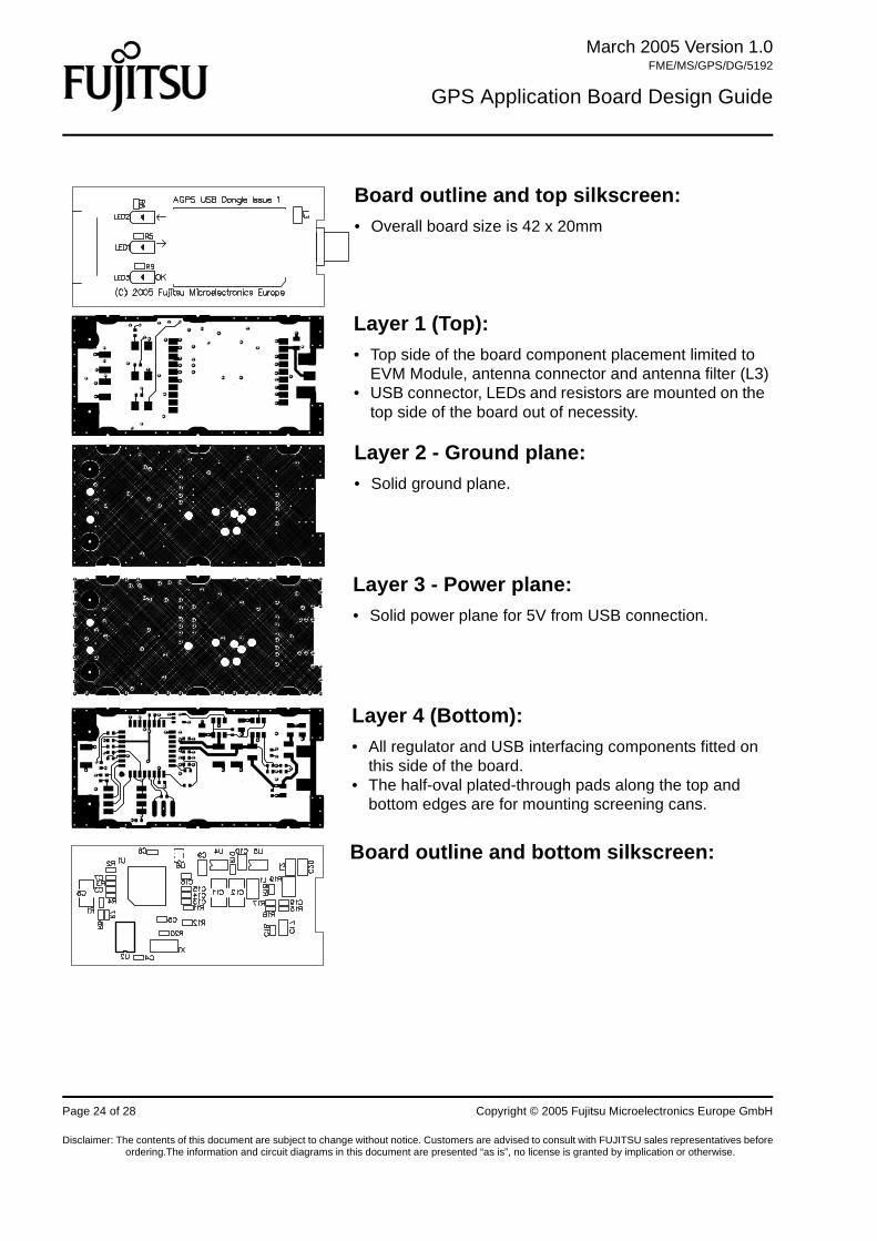
Board outline and top silkscreen:• Overall board size is 42 x 20mm
Layer 1 (Top):• Top side of the board component placement limited to
EVM Module, antenna connector and antenna filter (L3)• USB connector, LEDs and resistors are mounted on the
top side of the board out of necessity.
Layer 2 - Ground plane:• Solid ground plane.
Layer 3 - Power plane:• Solid power plane for 5V from USB connection.
Layer 4 (Bottom):• All regulator and USB interfacing components fitted on
this side of the board.• The half-oval plated-through pads along the top and
bottom edges are for mounting screening cans.
Board outline and bottom silkscreen:
Page 24 of 28 Copyright © 2005 Fujitsu Microelectronics Europe GmbH
Disclaimer: The contents of this document are subject to change without notice. Customers are advised to consult with FUJITSU sales representatives before ordering.The information and circuit diagrams in this document are presented “as is”, no license is granted by implication or otherwise.

March 2005 Version 1.0FME/MS/GPS/DG/5192
GPS Application Board Design Guide
Notes
Copyright © 2005 Fujitsu Microelectronics Europe GmbH Page 25 of 28
Disclaimer: The contents of this document are subject to change without notice. Customers are advised to consult with FUJITSU sales representatives before ordering.The information and circuit diagrams in this document are presented “as is”, no license is granted by implication or otherwise.

March 2005 Version 1.0FME/MS/GPS/DG/5192
GPS Application Board Design Guide
Notes
Page 26 of 28 Copyright © 2005 Fujitsu Microelectronics Europe GmbH
Disclaimer: The contents of this document are subject to change without notice. Customers are advised to consult with FUJITSU sales representatives before ordering.The information and circuit diagrams in this document are presented “as is”, no license is granted by implication or otherwise.

March 2005 Version 1.0FME/MS/GPS/DG/5192
GPS Application Board Design Guide
Notes
Copyright © 2005 Fujitsu Microelectronics Europe GmbH Page 27 of 28
Disclaimer: The contents of this document are subject to change without notice. Customers are advised to consult with FUJITSU sales representatives before ordering.The information and circuit diagrams in this document are presented “as is”, no license is granted by implication or otherwise.

28
Worldwide Headquarters
Japan AsiaTel: +81 44 754 3753Fax: +81 44 754 3329
Fujitsu LimitedKamikodanaka 4-1-1Nakahara-kuKawasaki-shiKanagawa-ken 211-8588Japan
Tel: +65 281 0770Fax: +65 281 0220
Fujitsu Microelectronics Asia Pte Ltd151 Lorong ChauanNew Tech Park#05-08Singapore 556741
http://www.fujitsu.com http://www.fmal.fujitsu.com
USA EuropeTel: +1 408 737 5600Fax: +1 408 737 5999
Fujitsu Microelectronics America, Inc.1250 E. Arques Avenue, M/S 333Sunnyvale, CA 94088-3470USA
Tel: +49 6103 6900Fax: +49 6103 690122
Fujitsu Microelectronics Europe GmbHAm Siebenstein 6-10D-63303 Dreieich-BuchschlagGermany
Tel: +1 800 866 8608Fax: +1 408 737 5984
Customer Response CenterMon-Fri: 7am-5pm (PST)
http://www.fma.fujitsu.com/ http://www.fme.fujitsu.com/
March 2005 Version 1.0FME/MS/GPS/DG/5192
GPS Application Board Design Guide
Page 28 of 28 Copyright © 2005 Fujitsu Microelectronics Europe GmbH
Disclaimer: The contents of this document are subject to change without notice. Customers are advised to consult with FUJITSU sales representatives before ordering.The information and circuit diagrams in this document are presented “as is”, no license is granted by implication or otherwise.
FME/MS/GPS/DG/5192 1.0
The contents of this document are subject to change without notice. Customers are advised to consult with FUJITSU sales representatives before ordering.
The information and circuit diagrams in this document presented as examples of semiconductor device applications, and are not intended to be incorporated in devices for actual use. Also, FUJITSU is unable to assume responsibility for infringement of any patent rights or other rights of third parties arising from the use of this information or circuit diagrams. No license is granted by implication or otherwise under any patent or patent rights of Fujitsu Microelectronics Europe GmbH.
FUJITSU semiconductor devices are intended for use in standard applications (computers, office automation and other office equipment, industrial, communications, and measurement equipment, personal or household devices, etc.).
CAUTION: Customers considering the use of our products in special applications where failure or abnormal operation may directly affect human lives or cause physical injury or property damage, or where extremely high levels of reliability are demanded (such as aerospace systems, atomic energy controls, sea floor repeaters, vehicle operating controls, medical devices for life support, etc.) are requested to consult with FUJITSU sales representatives before such use. The company will not be responsible for damages arising from such use without prior approval.
Any semiconductor devices have inherently a certain rate of failure. You must protect against injury, damage or loss from such failures by incorporating safety design measures into your facility and equipment such as redundancy, fire protection, and prevention of over-current levels and other abnormal operating conditions.
If any products described in this document represent goods or technologies subject to certain restrictions on export under the Foreign Exchange and Foreign Trade Control Law of Japan, the prior authorization by Japanese government should be required for export of those products from Japan.