Fundamentals of VLSI
65
Fundamentals of VLSI Introduction Andreas Burg Telecommunications Circuits Laboratory, EPFL, Switzerland
Transcript of Fundamentals of VLSI
Fundamentals of VLSI
Introduction
Andreas Burg
Telecommunications Circuits Laboratory, EPFL, Switzerland

How to design a complex digital integrated circuits using
modern design tools:
The basic building blocks (transistor-level design)
The basic building blocks (logic gates, memories, …)
Basic performance metrics and behavior of digital circuits
Designing complex circuits with design abstraction
Design abstraction with Hardware Description Languages
Froentend: From HDL to a digital integrated circuit
Backend: Physical design
At the end of the course, you should be able to
Understand all steps involved in the design process
Design an integrated circuit from specification to tapeout
Understand its behavior and optimize its performance
2

The course is divided into two parts:
Part-1: Fundamentals of digital integrated circuits
Design on transistor level => Full custom design
Consider the basic building blocks
Investigate the behavior of digital circuits on a small scale
Part-2: Managing complexity with abstraction
Design on the gate level => Semicustom design
Handle complex designs with millions of transistors
Understand and learn how to use the design tools
Design and optimization techniques
3
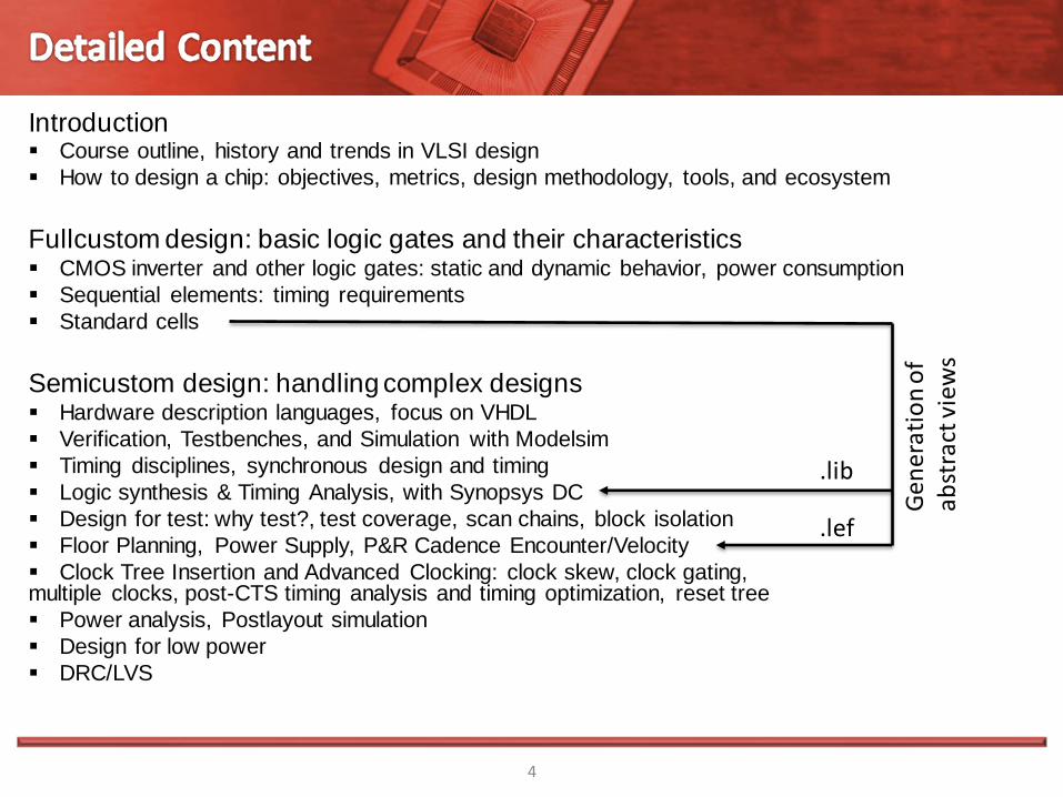
Introduction Course outline, history and trends in VLSI design
How to design a chip: objectives, metrics, design methodology, tools, and ecosystem
Fullcustom design: basic logic gates and their characteristics CMOS inverter and other logic gates: static and dynamic behavior, power consumption
Sequential elements: timing requirements
Standard cells
Semicustom design: handling complex designs Hardware description languages, focus on VHDL
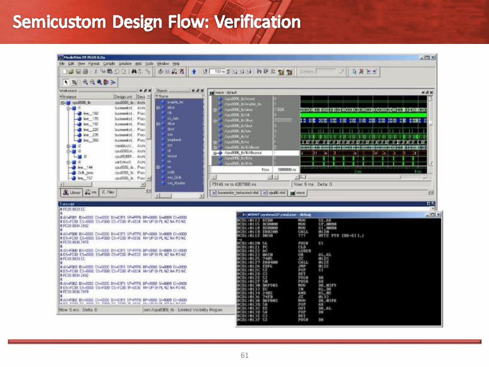
Verification, Testbenches, and Simulation with Modelsim
Timing disciplines, synchronous design and timing
Logic synthesis & Timing Analysis, with Synopsys DC
Design for test: why test?, test coverage, scan chains, block isolation
Floor Planning, Power Supply, P&R Cadence Encounter/Velocity
Clock Tree Insertion and Advanced Clocking: clock skew, clock gating, multiple clocks, post-CTS timing analysis and timing optimization, reset tree
Power analysis, Postlayout simulation
Design for low power
DRC/LVS
4
Gen
erat
ion
of
abst
ract
vie
ws
.lef
.lib

Classroom lectures cover 50% of the course hours and can
be Thursday and/or Friday
Mandatory exercises/Labs in irregular intervals based on
content of the course and can also be Thursday and/or Friday
(announced on Moodle)
Homework is the completion of the exercises
We highly recommend you attend also the optional EDA-
TP on Tuesady since it provides a lot of practical
background and additional practice for the exercises
5

Graded exercises will count 50% toward the final grade
Final exam counts 50% of your grade
Final exam will be similar to the exercises plus a quizz
Hint: make sure you attend all lectures and exercises
6

Fundamentals of VLSI
Lecture 1
Andreas Burg
Telecommunications Circuits Laboratory, EPFL, Switzerland
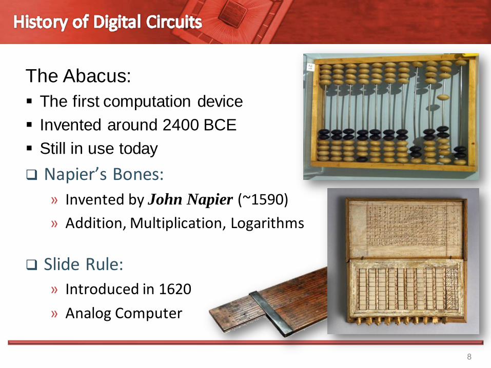
The Abacus:
The first computation device
Invented around 2400 BCE
Still in use today
8
Napier’s Bones:
» Invented by John Napier (~1590)
» Addition, Multiplication, Logarithms
Slide Rule:
» Introduced in 1620
» Analog Computer
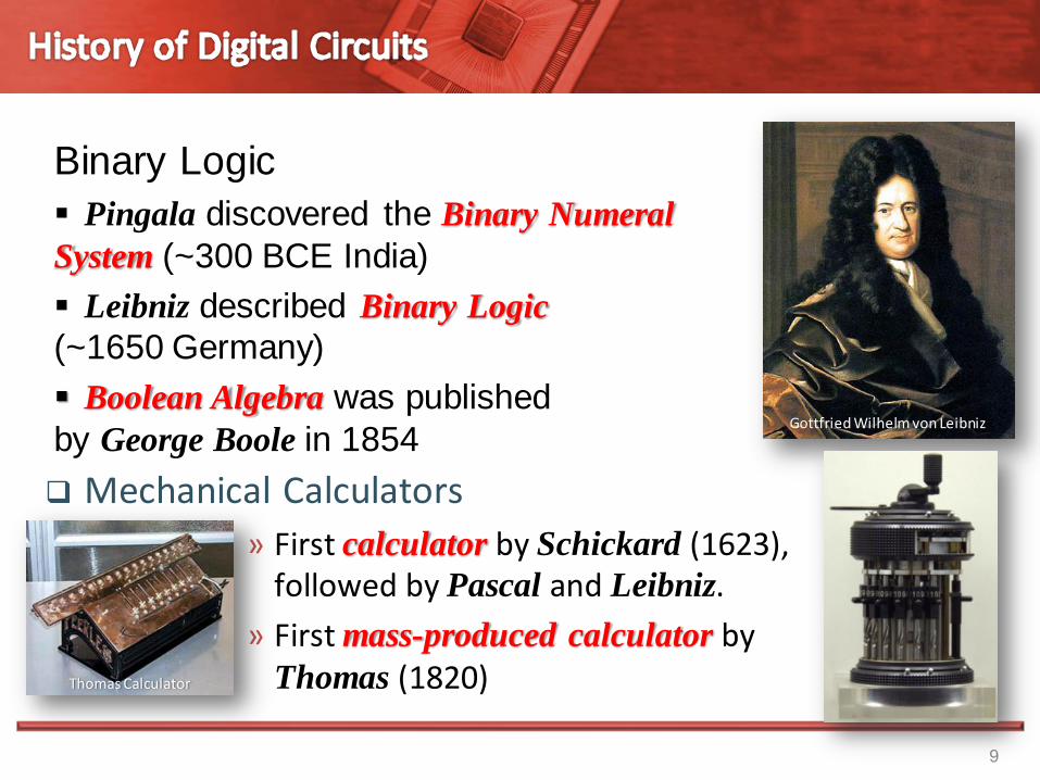
Binary Logic
Pingala discovered the Binary Numeral
System (~300 BCE India)
Leibniz described Binary Logic
(~1650 Germany)
Boolean Algebra was published
by George Boole in 1854
9
Gottfried Wilhelm von Leibniz
Mechanical Calculators
» First calculator by Schickard (1623), followed by Pascal and Leibniz.
» First mass-produced calculator by Thomas (1820) Thomas Calculator
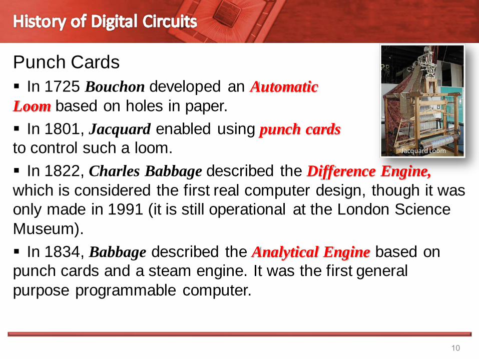
Punch Cards
In 1725 Bouchon developed an Automatic
Loom based on holes in paper.
In 1801, Jacquard enabled using punch cards
to control such a loom.
In 1822, Charles Babbage described the Difference Engine,
which is considered the first real computer design, though it was
only made in 1991 (it is still operational at the London Science
Museum).
In 1834, Babbage described the Analytical Engine based on
punch cards and a steam engine. It was the first general
purpose programmable computer.
10
Jacquard Loom
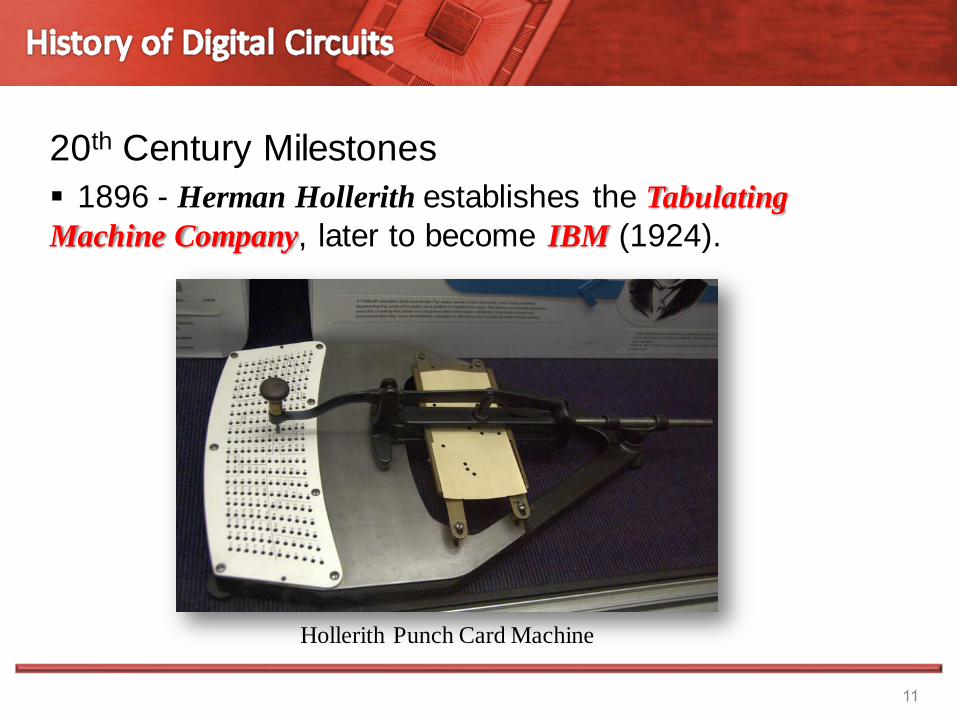
20th Century Milestones
1896 - Herman Hollerith establishes the Tabulating
Machine Company, later to become IBM (1924).
11
Hollerith Punch Card Machine

20th Century Milestones
1906 – The Electronic Valve is invented (De Forest). This is
the switch that enabled the development of the digital
computer.
1919 – The Flip Flop was proposed (Eccles, Jordan).
1937 – Alan Turing publishes paper describing the “Turing
Machine” and sets the basis for computer theory. Turing is
considered “The Father of Modern Day Computing”
12

13
The Alan Turing Memorial Statue in Manchester
The Enigma German Encryption Machine that Turing helped
decipher
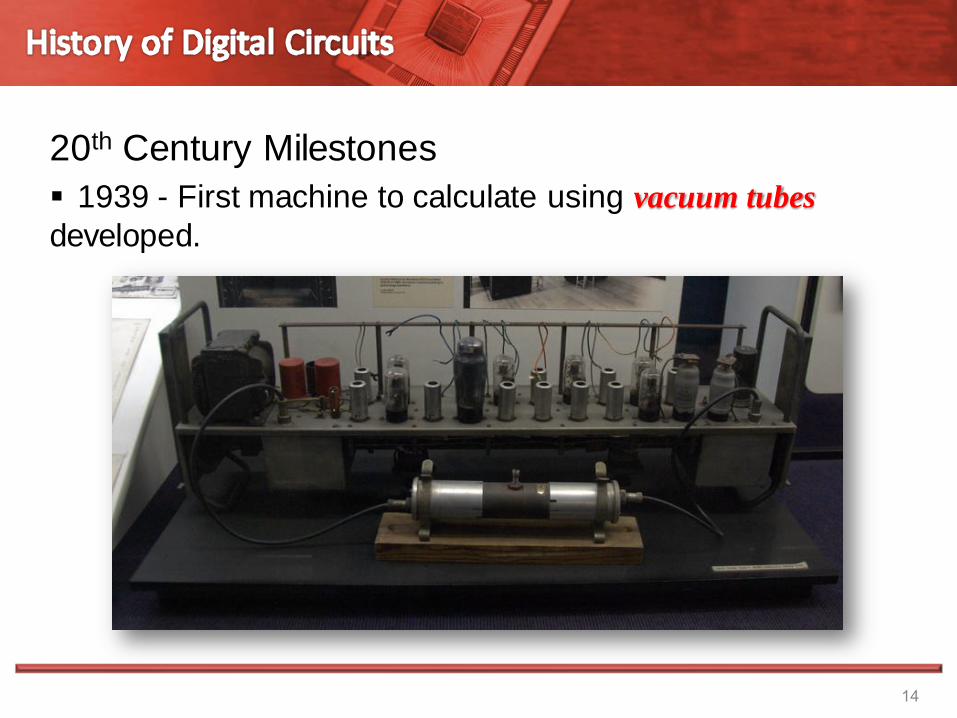
20th Century Milestones
1939 - First machine to calculate using vacuum tubes
developed.
14

15
ENIAC (1946) Considered the first Universal Electronic Computer. Used 18,000 electronic valves, weighed 30 Tons and consumed 25kW of power. Could do approximately 100,000 calculations a second. Intended to compute artillery firing tables (military)
UNIVAC-1 (1951) First commercially successful electronic computer. Also, first general purpose computer. Worked with magnetic tapes.

Grace Brewster Murray Hopper Inventor of the infamous Bug! The first “Bug”
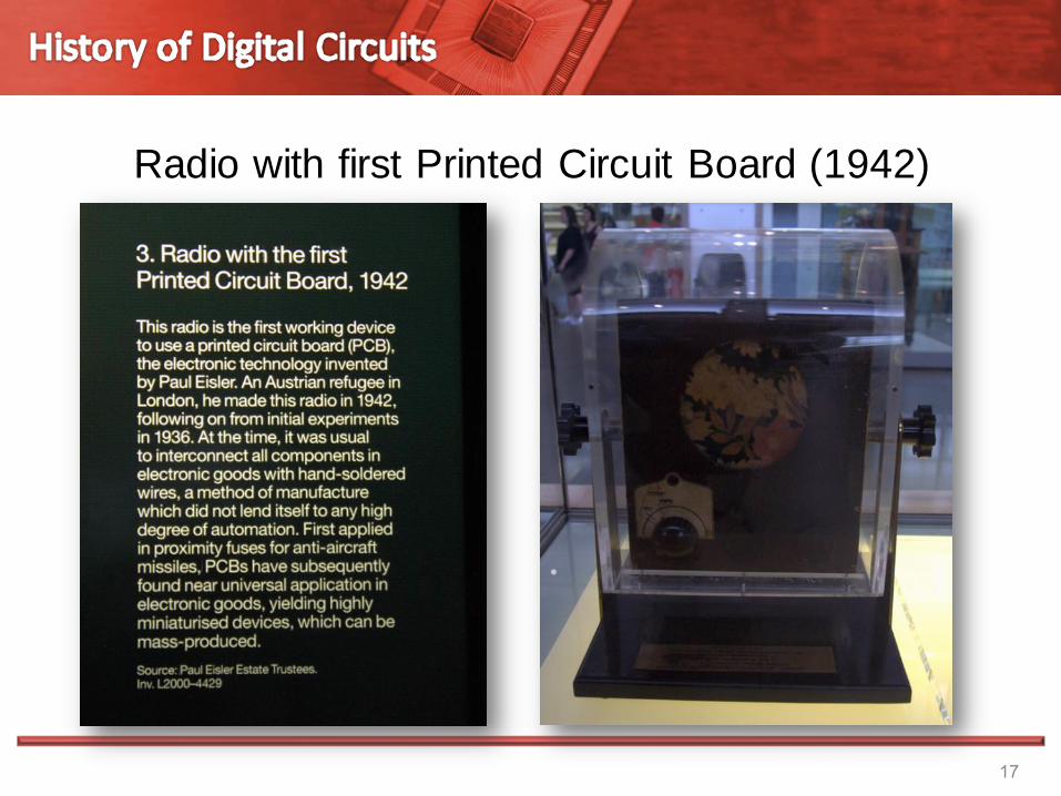
Radio with first Printed Circuit Board (1942)
17

The Transistor Era
1947 – A group at Bell Labs, headed
by Shockley, invent the first transistor
to replace the inefficient vacuum tube.
1952 – The idea of the Integrated
Circuit was conceived by Dummer.
18
The first Transistor
» 1958 – The first integrated circuit
was invented by Jack Kilby of TI.
The first silicon IC was invented
by Robert Noyce of Fairchild half a
year later. Kilby’s Integrated Circuit
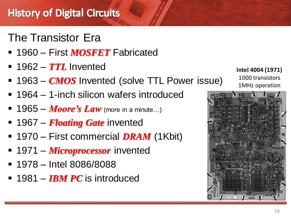
The Transistor Era
1960 – First MOSFET Fabricated
1962 – TTL Invented
1963 – CMOS Invented (solve TTL Power issue)
1964 – 1-inch silicon wafers introduced
1965 – Moore’s Law (more in a minute…)
1967 – Floating Gate invented
1970 – First commercial DRAM (1Kbit)
1971 – Microprocessor invented
1978 – Intel 8086/8088
1981 – IBM PC is introduced
19
Intel 4004 (1971) 1000 transistors 1MHz operation

The Xerox Alto (1973)
Mouse
Graphical Display
LAN
WYSIWYG Editor
Drawing Program
Windows UI
20
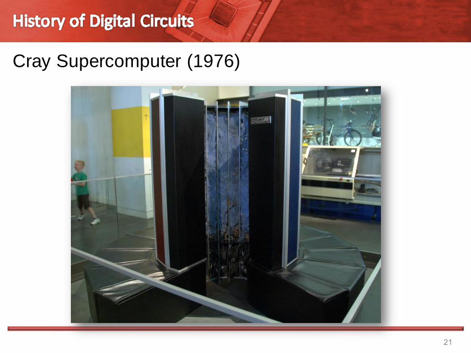
Cray Supercomputer (1976)
21
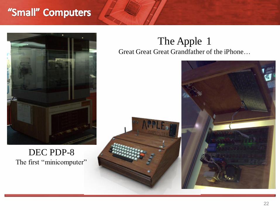
22
DEC PDP-8 The first “minicomputer”
The Apple 1 Great Great Great Grandfather of the iPhone…
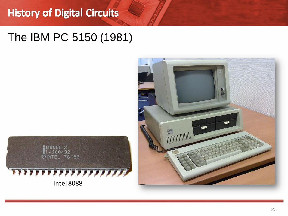
The IBM PC 5150 (1981)
23
Intel 8088

In 1965, Gordon Moore noted that the number of transistors on a
chip doubled every 18 to 24 months.
He made a prediction that semiconductor technology will
double its effectiveness every 18 months
24
1 6
1 5
1 4
1 3
1 2
1 1
1 0
9
8
7
6
5
4
3
2
1
0
19
59
19
60
19
61
19
62
19
63
19
64
19
65
19
66
19
67
19
68
19
69
19
70
19
71
19
72
19
73
19
74
19
75
LO
G2
OF
TH
E N
UM
BE
R O
F
CO
MP
ON
EN
TS
PE
R I
NT
EG
RA
TE
D F
UN
CT
ION
Electronics, April 19, 1965.

“The complexity for minimum component costs has
increased at a rate of roughly a factor of two per year.
Certainly over the short term, this rate can be expected to
continue, if not to increase. Over the longer term, the rate
of increase is a bit more uncertain, although there is no
reason to believe it will not remain nearly constant for at
least 10 years. That means by 1975, the number of
components per integrated circuit for minimum cost will be
65,000.”
Gordon Moore, Cramming more Components onto Integrated
Circuits, (1965).
25

The more devices
on a single IC, the
more functions we
can sell for the
same price.
26
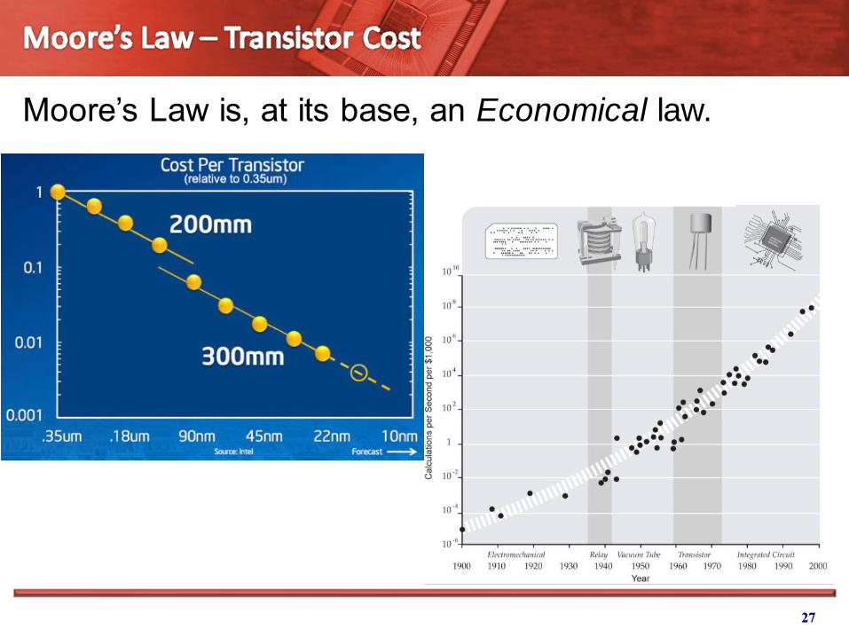
Moore’s Law is, at its base, an Economical law.
27
28
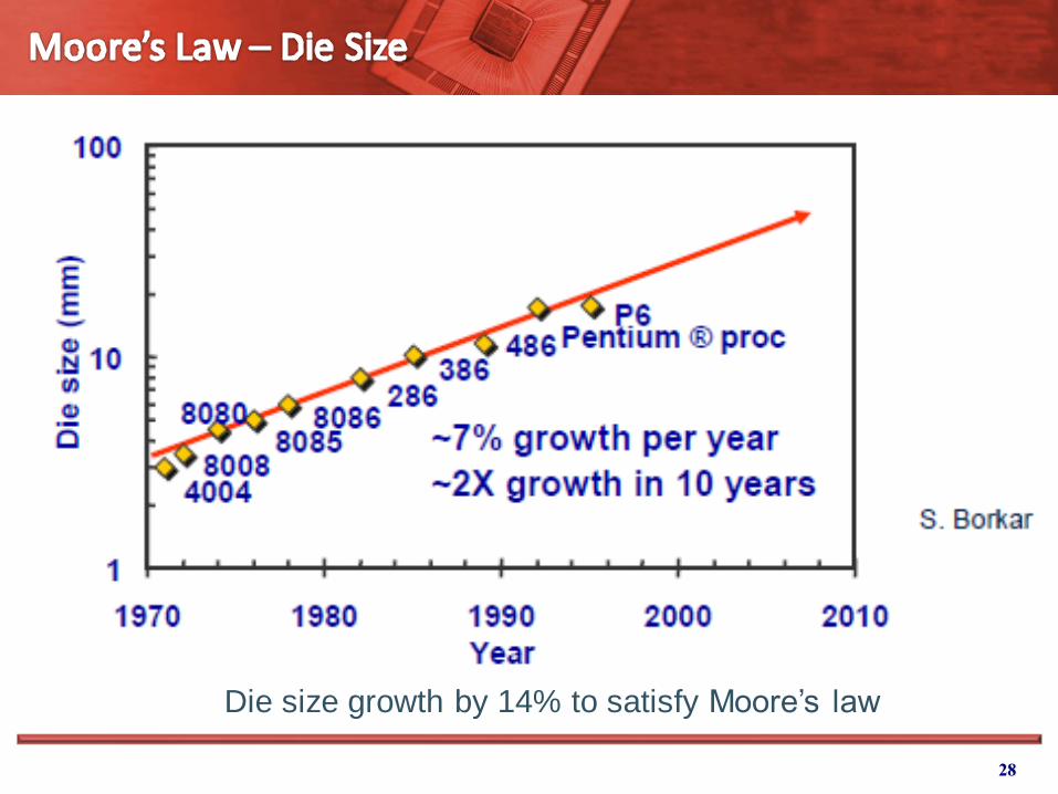
Die size growth by 14% to satisfy Moore’s law
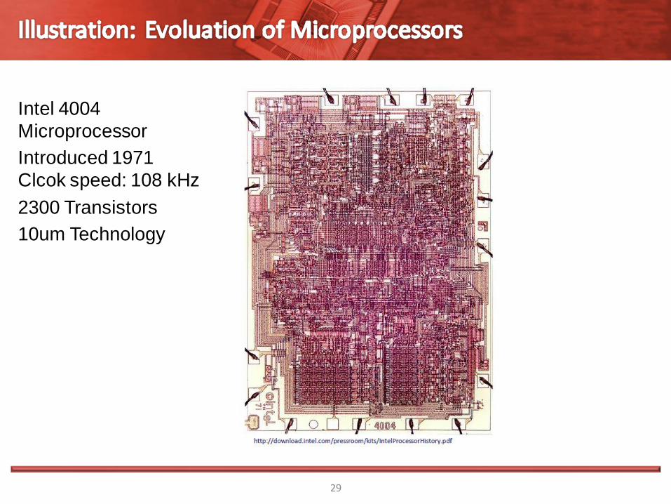
Intel 4004
Microprocessor
Introduced 1971
Clcok speed: 108 kHz
2300 Transistors
10um Technology
29

Intel 8088
Microprocessor
Introduced 1979
Clcok speed: 5 MHz
29’000 Transistors
3um Technology
30

Intel Pentium
Microprocessor
Introduced 1993
Clcok speed: 66 MHz
3.1 Mio Transistors
0.8um Technology
31

Intel Pentium 4
Microprocessor
Introduced 2000
Clcok speed: 1.5 GHz
42 Mio Transistors
0.18um Technology
32

Intel Core 2 Duo
Microprocessor
Introduced 2006
Clcok speed: 2.9 GHz
291 Mio Transistors
65nm Technology
Power: 65W
33

Quad-Core Intel Xeon
Microprocessor
Introduced 2007
Clcok speed: >3 GHz
820 Mio Transistors
45nm Technology
Power: 45W
34
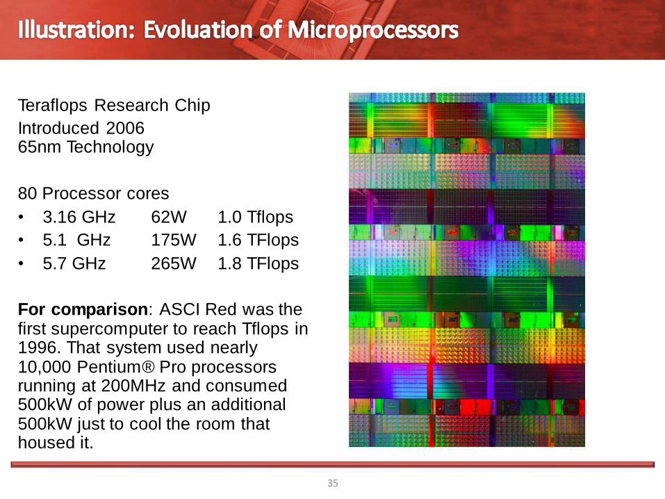
Teraflops Research Chip
Introduced 2006 65nm Technology
80 Processor cores
• 3.16 GHz 62W 1.0 Tflops
• 5.1 GHz 175W 1.6 TFlops
• 5.7 GHz 265W 1.8 TFlops
For comparison: ASCI Red was the first supercomputer to reach Tflops in 1996. That system used nearly 10,000 Pentium® Pro processors running at 200MHz and consumed 500kW of power plus an additional 500kW just to cool the room that housed it.
35

36
4004
8008
8080
8085
8086
286 386
486 Pentium®
P6
1
10
100
1000
10000
1970 1980 1990 2000 2010
Year
Po
wer
Den
sit
y (
W/c
m2)
Hot Plate
Nuclear
Reactor
Rocket
Nozzle
Sun’s
Surface
Source: Intel

37
Operating frequency saturates due to thermal limits Possible solution: lower frequency, more parellel processing
Need for low- power design

38
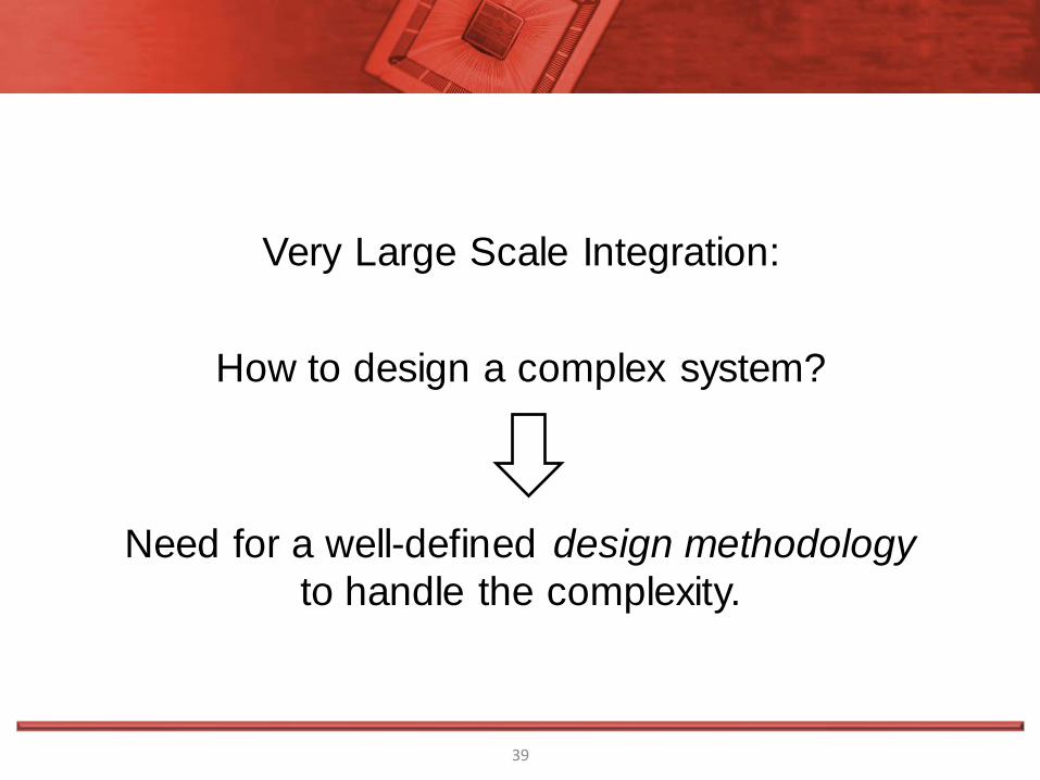
Very Large Scale Integration:
How to design a complex system?
Need for a well-defined design methodology
to handle the complexity.
39
40
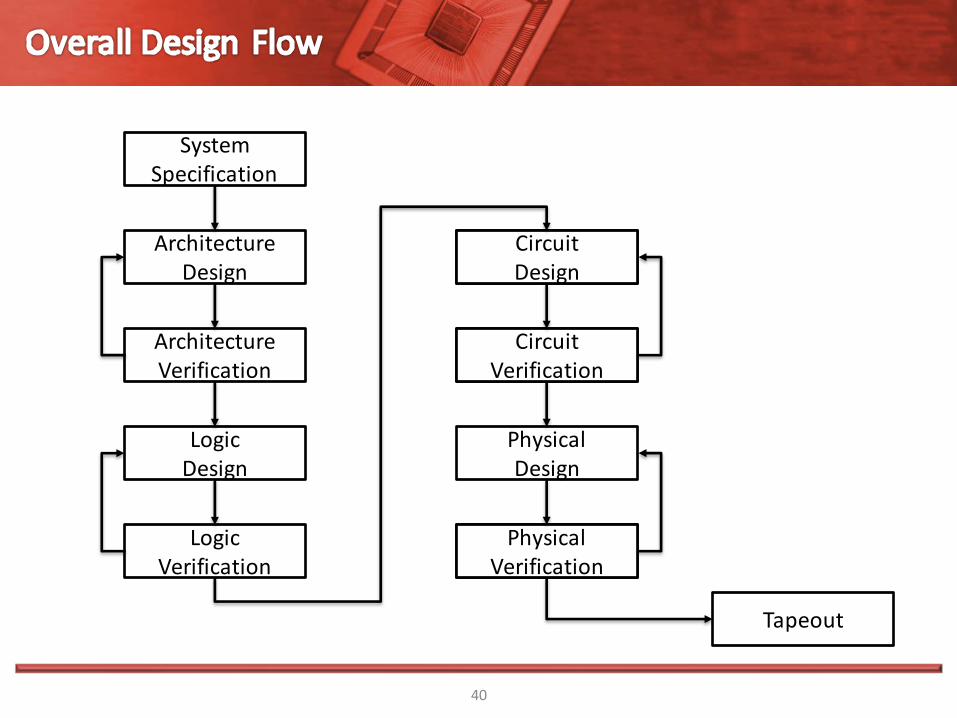
System Specification
Architecture Design
Architecture Verification
Logic Design
Logic Verification
Circuit Design
Circuit Verification
Circuit Design
Circuit Verification
Circuit Verification
Physical Design
Physical Verification
Tapeout

The golden rule: ALWAYS START WITH A BLOCK DIAGRAM!
41
Use hierarchy also in your block diagram
Identify blocks
What do we need to perform the
functionality
Visualize structure
How are blocks connected
Find critical paths
Which block is the most critical
(speed, area, power)?
Divide and Conquer
Use hierarchy, i.e., draw sub-block
diagrams

Hierarchy: “Divide and conquer” technique involves dividing a module into submodules and then repeating this operation on the sub-modules until the complexity of the smaller parts becomes manageable.
Regularity: The hierarchical decomposition of a large system should result in not only simple, but also similar blocks, as much as possible. Regularity usually reduces the number of different modules that need to be designed and verified, at all levels of abstraction.
Modularity: The various functional blocks which make up the larger system must have well-defined functions and interfaces.
Locality: Internal details remain at the local level. The concept of locality also ensures that connections are mostly between neighboring modules, avoiding longdistance connections as much as possible.
42
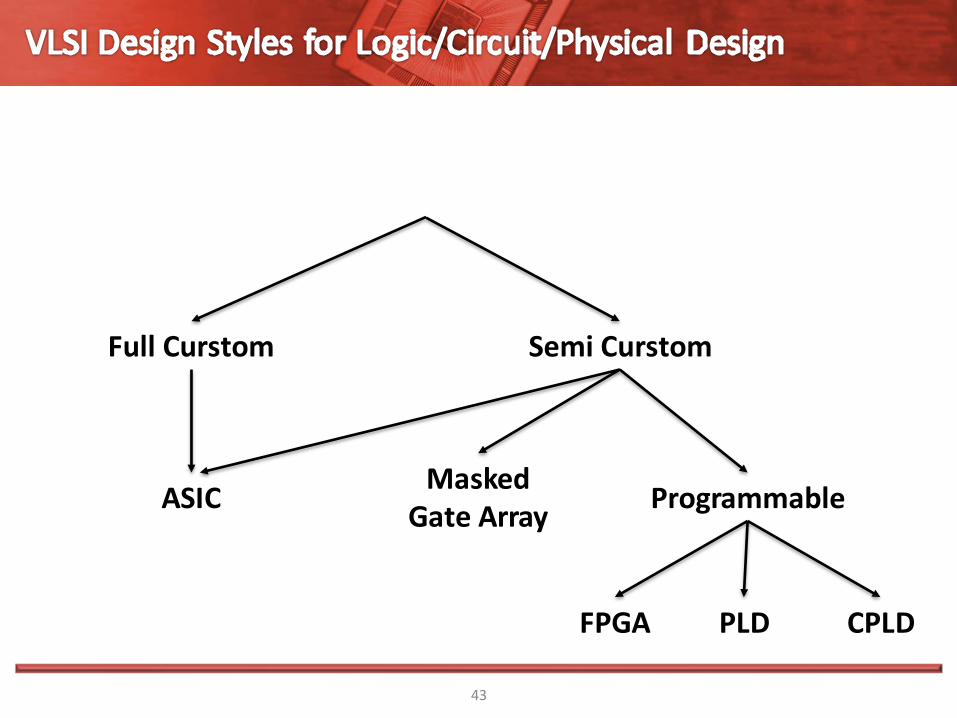
43
Full Curstom Semi Curstom
ASIC Masked
Gate Array Programmable
FPGA PLD CPLD
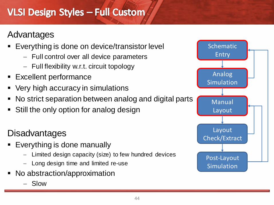
Advantages
Everything is done on device/transistor level
Full control over all device parameters
Full flexibility w.r.t. circuit topology
Excellent performance
Very high accuracy in simulations
No strict separation between analog and digital parts
Still the only option for analog design
Disadvantages
Everything is done manually
Limited design capacity (size) to few hundred devices
Long design time and limited re-use
No abstraction/approximation
Slow
44
Schematic Entry
Analog Simulation
Manual Layout
Layout Check/Extract
Post-Layout Simulation
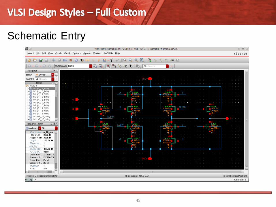
Schematic Entry
45

Simulation using Spice or Spectre
46
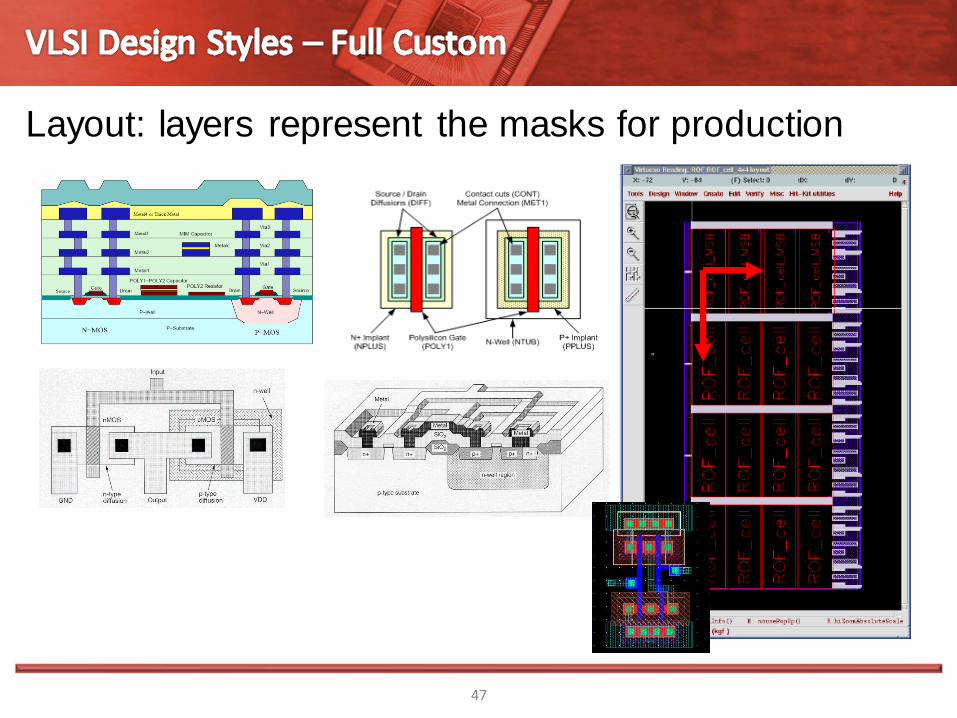
Layout: layers represent the masks for production
47
In full-custom style, the designer has many degrees of
freedom to optimize a circuit design:
Adjust individual transistor dimensions (width, length, aspect
ratio, etc.) to satisfy:
DC specifications (voltage levels, switching thresholds)
Transient specifications (delay times, rise- and fall-times)
Freely choose the most appropriate topology (placement and
routing) for each circuit block.
Decide on interconnection strategy between blocks.
Decide for the global distribution of power, ground and clock.
48

Increasing integration density no longer allows for design on
transistor level, neither on schematic, nor on layout level
Need for a more automated that leaves the details to EDA tools
49
Intel 8088, 1979 Full-custom design
Intel Pentium, 1993 Few macros, but mostly built
using automatic tools
Render the design process more efficiently by using
Hierarchy: build complex designs from a collection of smaller
and much simpler components which by themselves are again
hierarchical
Abstraction: simplified description/characterization of
components as a model (black box) to better use them on the
next level of hierarchy
Design automation: algorithms and tools to realize an
abstract design description from components
50

Layers of doped semiconductor material
or metal interconnect
Possible arrangemet of these layers is
determined by manufacturing process
Details are one of the best guarded secrets of
a foundry (years to develop)
Composition of layers determines
electrical and other characteristics
Characterized by the complex laws of physics
Technology Computer Aided Design (TCAD)
tools used for analysis and simulation
51
Technology
TCAD

Basic building blocks for circuit design that abstract the physics
of the technology layer to electrical characteristics
Foundries supply a Process Design Kit (PDK) which provides
Devices (Transistors, Resistors, Capacitors, Diodes)
Layers (e.g., for interconnect)
Various “Flavors” of PDKs are available, e.g.:
General Purpose/High Speed/Low Power
RF/Image Sensor
Flash/DRAM
Devices are abstracted to compact electrical
models for circuit simulations and design rules
Generated through TCAD and/or measurements
52
Technology
Devices
TCAD
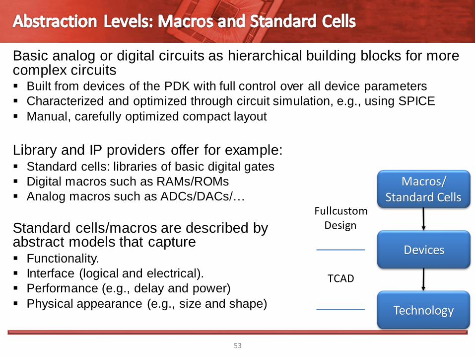
Basic analog or digital circuits as hierarchical building blocks for more complex circuits Built from devices of the PDK with full control over all device parameters
Characterized and optimized through circuit simulation, e.g., using SPICE
Manual, carefully optimized compact layout
Library and IP providers offer for example: Standard cells: libraries of basic digital gates
Digital macros such as RAMs/ROMs
Analog macros such as ADCs/DACs/…
Standard cells/macros are described by abstract models that capture Functionality.
Interface (logical and electrical).
Performance (e.g., delay and power)
Physical appearance (e.g., size and shape)
53
Technology
Devices
Macros/ Standard Cells
TCAD
Fullcustom Design

Complex digital blocks (IPs) and complete complex digital ICs
Specification of a digital circuit in a Hardware Description Language (HDL) Defines computational logic and storage elements in a abstract way
Semicustom design: Frontend: Automatic translation of HDL into a Gate-Level netlist (a circuit built from standard cells and macro blocks)
Backend: Physical implementation of the design based on basic building blocks
RTL designs can be abstracted through behavioral models
54
Technology
Devices
Macros/ Standard Cells
RTL Design
TCAD
Semicustom Design
Fullcustom Design
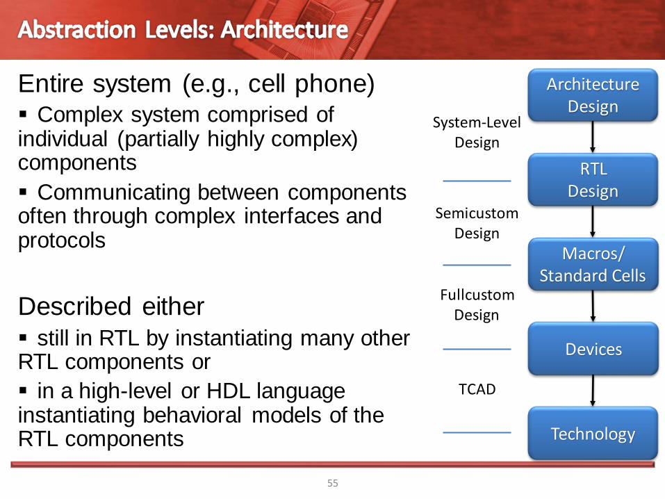
Entire system (e.g., cell phone) Complex system comprised of individual (partially highly complex) components
Communicating between components often through complex interfaces and protocols
Described either
still in RTL by instantiating many other RTL components or
in a high-level or HDL language instantiating behavioral models of the RTL components
55
Technology
Devices
Macros/ Standard Cells
RTL Design
Architecture Design
TCAD
Semicustom Design
Fullcustom Design
System-Level Design
56
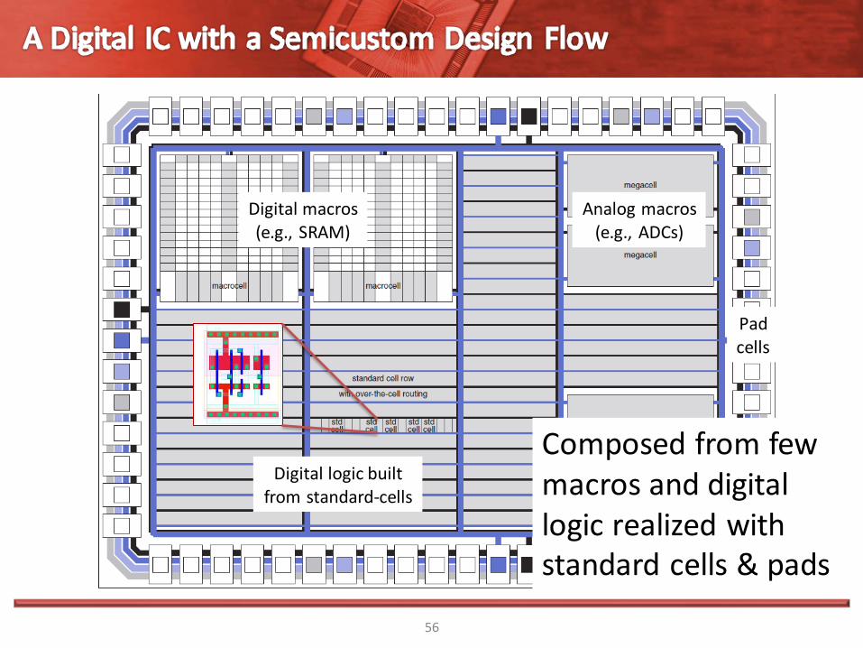
Digital logic built from standard-cells
Digital macros (e.g., SRAM)
Analog macros (e.g., ADCs)
Pad cells
Composed from few macros and digital logic realized with standard cells & pads
57
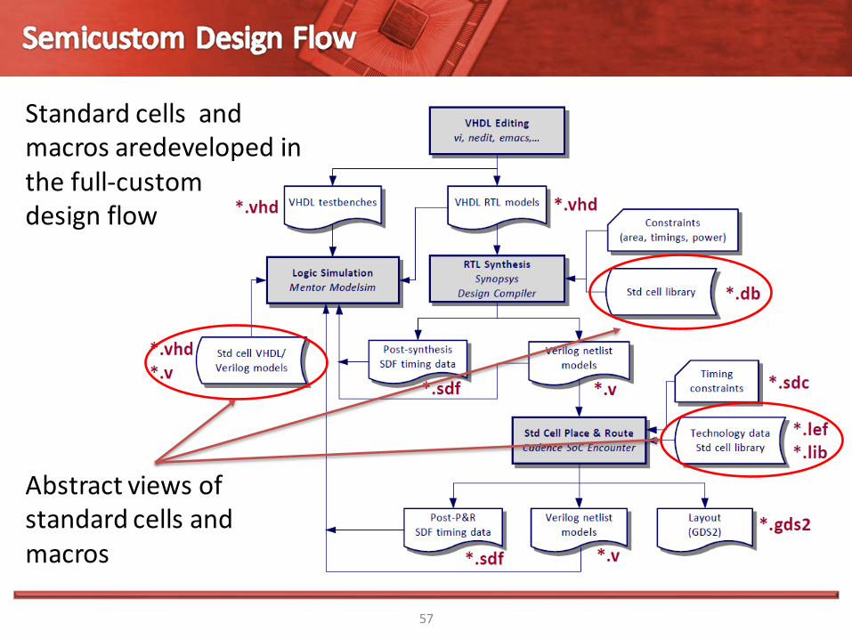
Standard cells and macros aredeveloped in the full-custom design flow
Abstract views of standard cells and macros

58
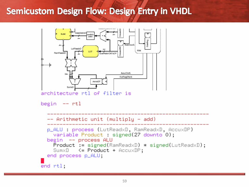
59
Modern hardware description languages allow structural
descriptions that basically determine all interconnections
between well-defined blocks:
adder: component adder port map (a,b,ci,co,s);
as well as purely behavioral descriptions like:
sum <= a + b - c;
The synthesizer is responsible for converting the behavioral
description into an optimized design.
60
61

62

63
64
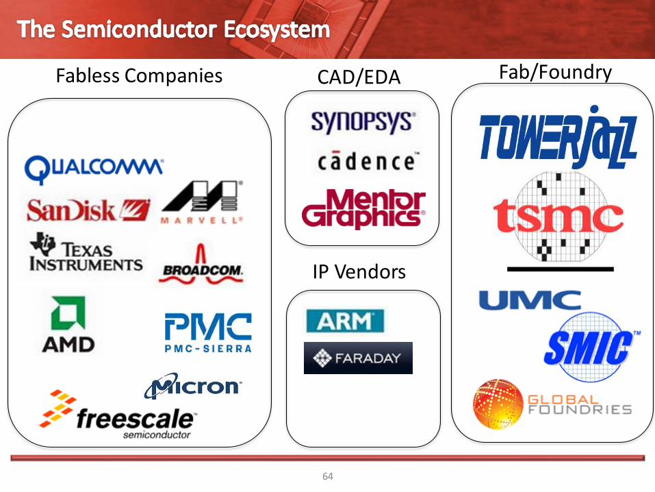
Fabless Companies Fab/Foundry CAD/EDA
IP Vendors

In VLSI Design, we always have a trade-off between:
For every circuit/system, we will have to evaluate the
specifications and choose the best trade-off that
meet any potential hard constraints on some metrics
In this class, we discussed the basic metrics and
relationship between Speed, Power, and Cost.
65
Speed Cost (Process/Area)
Reliability Power


![Ece-V-fundamentals of Cmos Vlsi [10ec56]-Notes](https://static.fdocuments.in/doc/165x107/55cf9c56550346d033a97884/ece-v-fundamentals-of-cmos-vlsi-10ec56-notes-56310235399c2.jpg)