Full Power Test System for Semiconductor Switching ...
61
ABSTRACT MURTHY, PRANAV. Design of a Full Power Test System for Semiconductor Switching Characterization. (Under the direction of Dr. Douglas C Hopkins.) Switching characterization of power semiconductors is commonly determined by Dou- ble Pulse Test. This method does not completely reflect real application circuit conditions like parasitic inductance and self heating of the device. Designing an application circuit specifically for switching loss calculation is expensive especially for high power circuits. In this thesis, an Energy Re-circulation based circuit is designed to test 6kV, 100A Super Cas- code Power Modules switching characteristics under full power conditions. The circuit uses inductor and capacitor to store energy and re-circulate at higher power levels than available from the supply. A complete system with cooling solution for test devices, controller for current regulation, bus bar for circuit connection and their assembly is presented.
Transcript of Full Power Test System for Semiconductor Switching ...

ABSTRACT
MURTHY, PRANAV. Design of a Full Power Test System for Semiconductor SwitchingCharacterization. (Under the direction of Dr. Douglas C Hopkins.)
Switching characterization of power semiconductors is commonly determined by Dou-
ble Pulse Test. This method does not completely reflect real application circuit conditions
like parasitic inductance and self heating of the device. Designing an application circuit
specifically for switching loss calculation is expensive especially for high power circuits. In
this thesis, an Energy Re-circulation based circuit is designed to test 6kV, 100A Super Cas-
code Power Modules switching characteristics under full power conditions. The circuit uses
inductor and capacitor to store energy and re-circulate at higher power levels than available
from the supply. A complete system with cooling solution for test devices, controller for
current regulation, bus bar for circuit connection and their assembly is presented.

© Copyright 2021 by Pranav Murthy
All Rights Reserved

Design of a Full Power Test System for SemiconductorSwitching Characterization
byPranav Murthy
A thesis submitted to the Graduate Faculty ofNorth Carolina State University
in partial fulfillment of therequirements for the Degree of
Master of Science
Electrical Engineering
Raleigh, North Carolina
2021
APPROVED BY:
Dr. Subhashish Bhattacharya Dr. Wensong Yu
Dr. Douglas C HopkinsChair of Advisory Committee

DEDICATION
To my mother for being the greatest source of strength and encouragement in my life.
ii

BIOGRAPHY
Pranav Murthy received his Bachelor’s degree in Electrical Engineering from University of
Mumbai in 2018. He joined North Carolina State University to pursue a Master’s degree in
2018 and has been working under the guidance of his advisor, Dr. Douglas C Hopkins, since
August 2019. His research interests include high voltage and high-density converter design
for power supplies.
iii

ACKNOWLEDGEMENTS
I would like to thank my advisor, Dr. Douglas C Hopkins, for his support and guidance
throughout my graduate studies. I am very grateful to Dr. Hopkins for providing me an
opportunity to work with him at the PREES lab and introducing me to Power Electronics
Packaging. His advice and encouragement has helped me think critically about technical
problems and become a better engineer. I would also like to thank my committee mem-
bers, Dr. Subhashish Bhattacharya and Dr. Wensong Yu, for serving on my committee and
providing valuable guidance and feedback.
I would like to thank my parents for supporting and enabling me to pursue my dreams.
This would have not been possible without their blessings.
Lastly, I would also like to thank all my friends, colleagues and lab mates at PREES for
their friendship and mutual support which made this journey more enjoyable. Special
thanks to Utkarsh and Tzu-Hsuan for always being available for technical discussions and
helping me to learn package processing in the lab.
iv

TABLE OF CONTENTS
LIST OF TABLES . . . . . . . . . . . . . . . . . . . . . . . . . . . . . . . . . . . . . . . . . . . . . . . . . . vi
LIST OF FIGURES . . . . . . . . . . . . . . . . . . . . . . . . . . . . . . . . . . . . . . . . . . . . . . . . . vii
Chapter 1 Introduction . . . . . . . . . . . . . . . . . . . . . . . . . . . . . . . . . . . . . . . . . . . 11.1 Overview . . . . . . . . . . . . . . . . . . . . . . . . . . . . . . . . . . . . . . . . . . . . . . . . . 11.2 Thesis Outline . . . . . . . . . . . . . . . . . . . . . . . . . . . . . . . . . . . . . . . . . . . . . 2
Chapter 2 Background and Literature Review . . . . . . . . . . . . . . . . . . . . . . . . . . 42.1 Static Characterization . . . . . . . . . . . . . . . . . . . . . . . . . . . . . . . . . . . . . . . 42.2 Dynamic Characterization . . . . . . . . . . . . . . . . . . . . . . . . . . . . . . . . . . . . 52.3 Full Power Test . . . . . . . . . . . . . . . . . . . . . . . . . . . . . . . . . . . . . . . . . . . . . 7
Chapter 3 Circuit Operation . . . . . . . . . . . . . . . . . . . . . . . . . . . . . . . . . . . . . . . 103.1 Operating principle . . . . . . . . . . . . . . . . . . . . . . . . . . . . . . . . . . . . . . . . . 10
3.1.1 Modes of operation . . . . . . . . . . . . . . . . . . . . . . . . . . . . . . . . . . . . 113.1.2 Switching pattern . . . . . . . . . . . . . . . . . . . . . . . . . . . . . . . . . . . . . 13
3.2 Component sizing . . . . . . . . . . . . . . . . . . . . . . . . . . . . . . . . . . . . . . . . . . 14
Chapter 4 Component Design . . . . . . . . . . . . . . . . . . . . . . . . . . . . . . . . . . . . . . 184.1 Super Cascode Power Module . . . . . . . . . . . . . . . . . . . . . . . . . . . . . . . . . . 194.2 Switching frequency . . . . . . . . . . . . . . . . . . . . . . . . . . . . . . . . . . . . . . . . . 224.3 Inductor . . . . . . . . . . . . . . . . . . . . . . . . . . . . . . . . . . . . . . . . . . . . . . . . . 244.4 Capacitor . . . . . . . . . . . . . . . . . . . . . . . . . . . . . . . . . . . . . . . . . . . . . . . . . 264.5 Power supply . . . . . . . . . . . . . . . . . . . . . . . . . . . . . . . . . . . . . . . . . . . . . . 28
Chapter 5 Virtual Test Setup . . . . . . . . . . . . . . . . . . . . . . . . . . . . . . . . . . . . . . . 305.1 Current control . . . . . . . . . . . . . . . . . . . . . . . . . . . . . . . . . . . . . . . . . . . . 305.2 Cooling system . . . . . . . . . . . . . . . . . . . . . . . . . . . . . . . . . . . . . . . . . . . . 375.3 Bus bar design . . . . . . . . . . . . . . . . . . . . . . . . . . . . . . . . . . . . . . . . . . . . . 415.4 System Assembly . . . . . . . . . . . . . . . . . . . . . . . . . . . . . . . . . . . . . . . . . . . 47
Chapter 6 Conclusion and Future work . . . . . . . . . . . . . . . . . . . . . . . . . . . . . . . 496.1 Scope of future work . . . . . . . . . . . . . . . . . . . . . . . . . . . . . . . . . . . . . . . . . 49
Bibliography . . . . . . . . . . . . . . . . . . . . . . . . . . . . . . . . . . . . . . . . . . . . . . . . . . . . 50
v

LIST OF TABLES
Table 4.1 Full Power Test Specification . . . . . . . . . . . . . . . . . . . . . . . . . . . . . 18Table 4.2 SCPM Specifications . . . . . . . . . . . . . . . . . . . . . . . . . . . . . . . . . . . 19Table 4.3 Switching Loss Energy of SCPM string . . . . . . . . . . . . . . . . . . . . . . 22Table 4.4 Capacitor Specifications . . . . . . . . . . . . . . . . . . . . . . . . . . . . . . . . 28Table 4.5 Estimate of maximum power loss during test . . . . . . . . . . . . . . . . . 29
Table 5.1 Partial inductance of bus bars . . . . . . . . . . . . . . . . . . . . . . . . . . . . 45
vi
LIST OF FIGURES
Figure 2.1 Typical Double Pulse Test Circuit . . . . . . . . . . . . . . . . . . . . . . . . . 5Figure 2.2 Typical Double Pulse Test Waveform . . . . . . . . . . . . . . . . . . . . . . . 6Figure 2.3 Ideal ERSC Buck Boost [8] . . . . . . . . . . . . . . . . . . . . . . . . . . . . . . . 7Figure 2.4 Full Power Test Circuit . . . . . . . . . . . . . . . . . . . . . . . . . . . . . . . . . 8Figure 2.5 IGCT Test circuit [11] . . . . . . . . . . . . . . . . . . . . . . . . . . . . . . . . . . 9Figure 2.6 Opposition Method cell [6] . . . . . . . . . . . . . . . . . . . . . . . . . . . . . . 9
Figure 3.1 Full Power Test Circuit . . . . . . . . . . . . . . . . . . . . . . . . . . . . . . . . . 11Figure 3.2 Mode 1 . . . . . . . . . . . . . . . . . . . . . . . . . . . . . . . . . . . . . . . . . . . . 11Figure 3.3 Mode 2 . . . . . . . . . . . . . . . . . . . . . . . . . . . . . . . . . . . . . . . . . . . . 12Figure 3.4 Mode 3 . . . . . . . . . . . . . . . . . . . . . . . . . . . . . . . . . . . . . . . . . . . . 12Figure 3.5 Mode 4 . . . . . . . . . . . . . . . . . . . . . . . . . . . . . . . . . . . . . . . . . . . . 13Figure 3.6 Inductor current build up . . . . . . . . . . . . . . . . . . . . . . . . . . . . . . . 14Figure 3.7 Steady state waveform . . . . . . . . . . . . . . . . . . . . . . . . . . . . . . . . . 15
Figure 4.1 SCPM Test Schematic . . . . . . . . . . . . . . . . . . . . . . . . . . . . . . . . . . 20Figure 4.2 SCPM switching OFF time . . . . . . . . . . . . . . . . . . . . . . . . . . . . . . 21Figure 4.3 SCPM switching ON time . . . . . . . . . . . . . . . . . . . . . . . . . . . . . . . 21Figure 4.4 SCPM Cross section along J6 . . . . . . . . . . . . . . . . . . . . . . . . . . . . 23Figure 4.5 LT Spice Schematic of Full Power Test . . . . . . . . . . . . . . . . . . . . . . 25Figure 4.6 FPT Results from LT Spice . . . . . . . . . . . . . . . . . . . . . . . . . . . . . . 25Figure 4.7 Inductor coil cross section . . . . . . . . . . . . . . . . . . . . . . . . . . . . . . 27Figure 4.8 FEMM Simulation Results . . . . . . . . . . . . . . . . . . . . . . . . . . . . . . 27
Figure 5.1 Circuit waveform with D1+D2 = 1 . . . . . . . . . . . . . . . . . . . . . . . . . 32Figure 5.2 Circuit waveform with D1+D2 > 1 . . . . . . . . . . . . . . . . . . . . . . . . . 33Figure 5.3 Pulse Width Modulator Block diagram . . . . . . . . . . . . . . . . . . . . . 34Figure 5.4 Current control block diagram . . . . . . . . . . . . . . . . . . . . . . . . . . . 34Figure 5.5 Bode Plot: Uncompensated loop . . . . . . . . . . . . . . . . . . . . . . . . . 35Figure 5.6 Bode plot of Compensated system . . . . . . . . . . . . . . . . . . . . . . . . 37Figure 5.7 Startup response for Step input . . . . . . . . . . . . . . . . . . . . . . . . . . 38Figure 5.8 Cooling system . . . . . . . . . . . . . . . . . . . . . . . . . . . . . . . . . . . . . . 38Figure 5.9 Parasitics in Full Power Test circuit . . . . . . . . . . . . . . . . . . . . . . . . 42Figure 5.10 Bus bar layout for FPT . . . . . . . . . . . . . . . . . . . . . . . . . . . . . . . . . 43Figure 5.11 Bus bar layout in Q3D . . . . . . . . . . . . . . . . . . . . . . . . . . . . . . . . . 44Figure 5.12 Current density plot of plates Pp at 100A DC . . . . . . . . . . . . . . . . . 46Figure 5.13 Current density plot of plates Pn at 100A DC . . . . . . . . . . . . . . . . . 46Figure 5.14 FPT SolidWorks assembly . . . . . . . . . . . . . . . . . . . . . . . . . . . . . . . 47Figure 5.15 Close up of Top View . . . . . . . . . . . . . . . . . . . . . . . . . . . . . . . . . . 48
vii

CHAPTER
1
INTRODUCTION
1.1 Overview
Power semiconductors are considered to be the most important components in modern
power processing equipment from grid applications, electric vehicles, motor drives to
low power household applications. Therefore it is important to accurately analyse and
design compact and efficient systems. Semiconductor testing plays an important role in
characterization and determining reliability of new devices. Silicon Carbide MOSFETs
are considered as leading candidates to replace IGBTs in medium voltage (2.5kV - 15kV)
applications. Authors in [1] have demonstrated the use of low voltage JFETs and MOSFETs
to build Supercascode switch structures which have low ON resistances and capable of fast
switching at high voltages.
1

In order to investigate new power electronic circuit topologies it is important to have ac-
curate loss models of these semiconductor devices. Typically, characterization tests for new
MOSFETs include Static and Dynamic tests. Static tests in [2],[3],[4],[5] are performed using
curve tracers such as Keysight B1015A which can completely define the device output and
transfer characteristics, on state resistance, threshold voltages, and junction capacitances.
A dynamic test includes Double Pulse Testing which switches a MOSFET under inductive
load to determine switching characteristics. This, however, does not accurately predict
the switching behavior in an application because of different operating conditions. These
differences can be circuit parasitics in the commutation loop, device parasitic capacitance
and distortions caused by probes and cables[6],[7]. Building an identical test system to the
application circuit only to evaluate devices at rated conditions would be expensive and
time-consuming especially for high power application.
This thesis explores how circuits based on Energy Re-circulation topology can be used
to perform full power tests [8]. The operation and virtual design of a 6kV,100A test circuit
will be discussed in detail here. Because of the 2020 pandemic, the Full Power Test circuit
demonstration was limited to a virtual circuit design.
1.2 Thesis Outline
This thesis is divided into 4 parts
• Chapter 2 provides background to Full Power Test circuit and how it is related to the
other test methods.
• Chapter 3 discusses the working of the circuit and formulate equations for system
sizing
• Chapter 4 discusses the design of passive components and selection of switching
frequency
2

• Chapter 5 details the design of current controller, cooling system, bus bar and shows
the assembly of the system
3

CHAPTER
2
BACKGROUND AND LITERATURE
REVIEW
This chapter discusses the Static and Dynamic methods used to characterise electrical
behaviour of switching power semiconductors. The drawbacks of the classical methods are
listed and compared to the advantages of the Full Power Test method.
2.1 Static Characterization
A static characterization test is used to determine the DC and AC behaviour of a MOSFET.
This includes output and transfer characteristics, on state resistance, threshold voltage and
junction capacitances. References [2],[3],[4],[5] show the static characterization process
4
on newly developed high voltage SiC MOSFETs using a Curve Tracer, Impedance analyser
and hot plate to test over a range of temperature. This test is important to understand the
working principle and operating limits of the Device Under Test (DUT). The next section
describes how switching performance is evaluated for a DUT.
2.2 Dynamic Characterization
A Double Pulse Test (DPT) is commonly used to characterize dynamic behaviour of MOS-
FETs. This test is carried out by switching a clamped inductive load on and off at a set
current. It can be used to measure turn on and turn off time, current and voltage rise times,
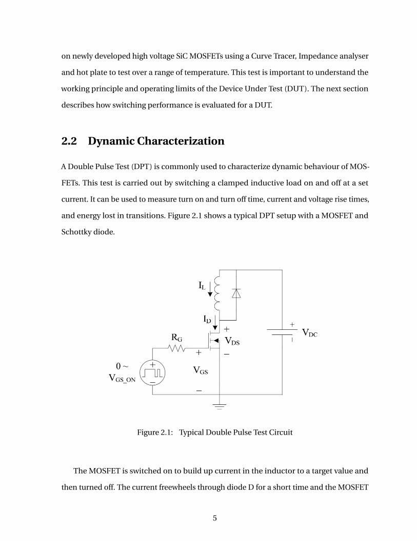
and energy lost in transitions. Figure 2.1 shows a typical DPT setup with a MOSFET and
Schottky diode.
Figure 2.1: Typical Double Pulse Test Circuit
The MOSFET is switched on to build up current in the inductor to a target value and
then turned off. The current freewheels through diode D for a short time and the MOSFET
5
is switched back on. The inductor L is sized such that the load current remains nearly
constant during freewheeling when the current commutates from MOSFET to diode or the
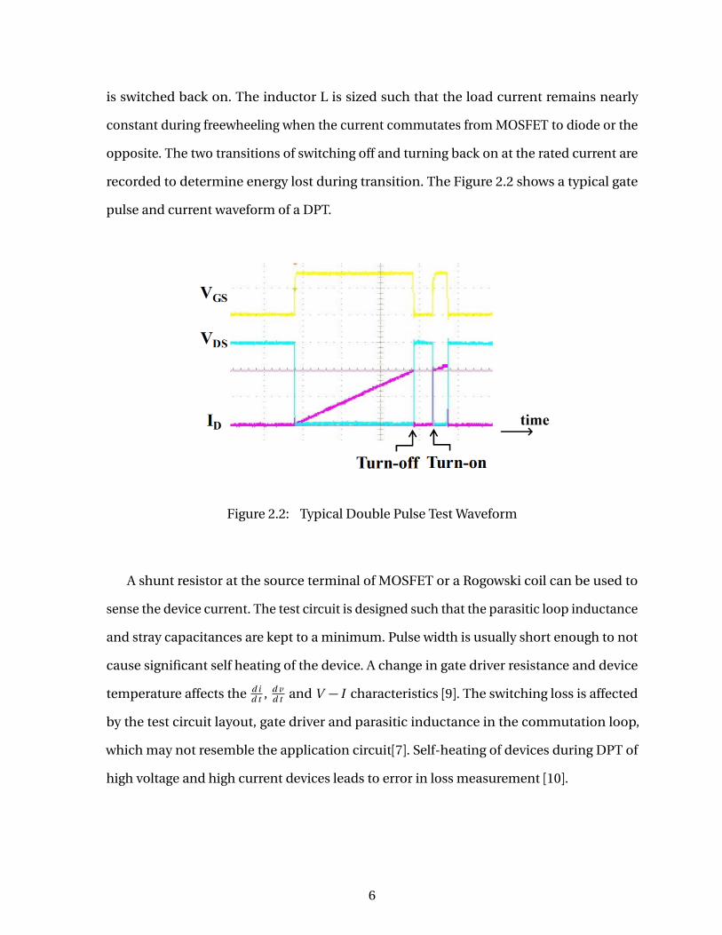
opposite. The two transitions of switching off and turning back on at the rated current are
recorded to determine energy lost during transition. The Figure 2.2 shows a typical gate
pulse and current waveform of a DPT.
Figure 2.2: Typical Double Pulse Test Waveform
A shunt resistor at the source terminal of MOSFET or a Rogowski coil can be used to
sense the device current. The test circuit is designed such that the parasitic loop inductance
and stray capacitances are kept to a minimum. Pulse width is usually short enough to not
cause significant self heating of the device. A change in gate driver resistance and device
temperature affects the d id t , d v
d t and V − I characteristics [9]. The switching loss is affected
by the test circuit layout, gate driver and parasitic inductance in the commutation loop,
which may not resemble the application circuit[7]. Self-heating of devices during DPT of
high voltage and high current devices leads to error in loss measurement [10].
6

2.3 Full Power Test
The classical methods of semiconductor testing have some shortcomings in accurately
predicting switching losses as discussed in the previous section. A straightforward way
to evaluate losses accurately would be to build an identical test system for this purpose.
Although, it might become very difficult and expensive especially for high power applica-
tions.
In [8] a new class of switched mode circuit called Energy Re-circulation and Storage
Circuits (ERSC) is introduced. This circuit pumps in and stores energy in inductor and
capacitor to create higher flow of power than the source provides, and dissipates it in the
device under test. Figure 2.3 shows a Boost-Buck ERSC in which the energy re-circulates
between L and C and the power supply only provides for the losses in semiconductors.
Switch S1 is modulated independently to control I1 and switch S2 controls voltage Vc and
I2.
Figure 2.3: Ideal ERSC Buck Boost [8]
The main circuit under consideration for this thesis is obtained by modifying the Boost-
7

Buck converter to an Asymmetric half bridge converter as shown in Figure 2.4. This change
limits capacitor to a fixed voltage and only inductor current can be ramped up. Inductor
current increases when both S1, S2 are ON and it decreases when both switches are off.
When only one of the switches is ON, the current freewheels with the diode.
Figure 2.4: Full Power Test Circuit
A similar circuit is used in [11] to perform device characterization of low voltage IGCTs
(1.5kV) and diodes (3.3kV) under real working conditions. Figure 2.5 shows the test circuit
with two opposing switching cells connected by an inductor known as the Opposition
Method. A current control loop is used to vary the load from 0 to 2kA at different switching
frequencies. The device power losses are measured using calorie meter and power analyzer.
By expanding this circuit to a Full bridge topology, [6] demonstrates a full power emu-
lation with GaN devices under hard and soft switching conditions. Figure 2.6 shows the
circuit used for this test.
8

Figure 2.5: IGCT Test circuit [11]
Figure 2.6: Opposition Method cell [6]
9

CHAPTER
3
CIRCUIT OPERATION
This chapter discusses the design and operation of the Full Power test circuit used in this
thesis.
3.1 Operating principle
Figure 3.1 shows the test circuit power stage derived from the ERSC Boost-Buck converter.
A single MOSFET and diode connection form a switching cell which are connected in
opposition to form this circuit. A DC link capacitor stores the recirculating energy. The DC
power supply is used to supply the losses of the circuit. Resistor Rs up is for current limiting
the power supply.
In this thesis a ’Virtual Design’ of a 6kV,100A setup for Full Power test of the 100A Super
10

Figure 3.1: Full Power Test Circuit
Cascode Power Module (SCPM) [1]will be presented in Chapter 4.
3.1.1 Modes of operation
Assuming the control loop has reached steady state for the set value of current the following
modes can be identified.
Mode 1 (Fig.3.2): Current build up - MOSFETs Q1 and Q2 are conducting and induc-
tor current, IL starts rising from its lowest value Imi n . The inductor current ripple, ∆I is
controlled by adjusting the overlap time, to for which Q1, Q2 are both ON. Voltage across
inductor is (Vc a p − IL (2Rd s O N +Rl )) where, Vc a p is the voltage across capacitor, Rd s O N is
the ON resistance of the MOSFET and Rl is the Equivalent Series Resistance (ESR) of the
inductor.
Figure 3.2: Mode 1
11

Mode 2 (Fig.3.3): Re-circulation - As the current reaches it highest value Ima x , switch Q1
is turned off and current commutates from Q1 to D1. If the device losses are low, inductor
current is held almost constant in this state. Switch Q2 remains ON.
Figure 3.3: Mode 2
Mode 3 (Fig.3.4): Current reduction - Switch Q2 is turned off and diodes D1, D2 starts
conducting. Voltage across inductor L becomes (−Vc a p +2Vf + Il ∗Rd s O N ) where, Vf is the
forward voltage drop of the diode. The current starts reducing as (−VL
d id t ) and charges the
capacitor.
Figure 3.4: Mode 3
Mode 4 (Fig.3.5): Re-circulation - After the inductor current reaches Imi n , switch Q1 is
turned back ON. The current commutates from Q2 to D2 and re-circulates through Q1 and
12

D2.
Figure 3.5: Mode 4
3.1.2 Switching pattern
In this circuit the current can be built up to any desired level by forcing a net positive
volt-sec product across the inductor using a current control method. The switch Q2 is set
to a fixed duty of 0.5 and the switch Q1 is controlled by the regulator. The Fig.3.6 shows
build up of current when d 1+d 2> 1 where d1 and d2 are duty cycles of switches Q1 and
Q2 respectively.
At steady state, when the average inductor current reaches a set value, the duty d1 settles
to a value slightly above 0.5 to compensate for the losses in the circuit. This time difference
in duty cycle between d 1 and d 2 is defined as ε, which can be calculated by using the
formula[12]:
ε=Pl o s s
Pi n ∗ fs w(3.1)
The gate pulses of Q1 and Q2 are phase shifted in time, defined asΦ (sec), which reduces
the value of inductance required for a certain allowed ripple.
13

Figure 3.6: Inductor current build up
3.2 Component sizing
Power stage loss estimation: The capacity of a power supply will be determined by the
total circuit and DUT losses to be compensated. The circuit is expected to have conduction
and switching losses in the semiconductors and parasitic resistance in the passives. The
total power recirculating in the circuit at steady state will be E ∗ IL where E is the DC link
voltage and IL is the average inductor current. Only a fraction of this will be lost as active
power. Therefore the power source should be sized according to the sum of all the expected
losses and some margin above it.
The current through the MOSFETs Q1,Q2 can be approximated to a square wave shape
since∆I is small compared to IL .
14

Figure 3.7: Steady state waveform
15

Ir m s = Ima x ∗p
D (3.2)
Ia v g = Ima x ∗D (3.3)
where, Ir m s is the Root Mean Square (RMS) of the current through MOSFETs, Ima x is
the highest value of current through Q1,Q2 and D is the duty cycle of the switches.
Therefore, the MOSFET conduction and switching losses can be estimated as:
Pc o nd = I 2r m s ∗Rd s O N (3.4)
Ps w = (Eo n +Eo f f ) ∗ fs w (3.5)
where, fs w is the switching frequency and Eo n , Eo f f are the ON and OFF switching
energy of the MOSFET.
Diode losses can be estimated as:
Pc o nd =Vf ∗ Ia v g + I 2r m s ∗Rd (3.6)
Ps w =Qc ∗Vo u t ∗ fs w (3.7)
where, Qc is the total junction charge at voltage V, Rd is the equivalent resistance and
Vf is the forward voltage of the diode.
Assuming an air core inductor, the copper losses due to its DC resistance can be calcu-
lated as:
Pi nd = I 2L a v g ∗RL (3.8)
16

where, RL is the equivalent series resistance of the inductor.
Switching Frequency: In this test the SCPM is selected for evaluation which is based on
fast switching Silicon Carbide JFETs. The switching frequency for test can be selected based
on the type of application circuit that the SCPM is intended to be used in. The maximum
switching frequency for test under full power will depend on total module losses and the
cooling capacity of the cold plates.
Inductor: As seen from figure 3.7, for a fixed current ripple, inductance L is directly
dependent on the overlap time (to ) between Q1 and Q2. For a given test condition where
E is the maximum DC link voltage and ∆I is the maximum allowed ripple current, the
required inductance value can be defined as:
L =E ∗ to
∆I(3.9)
Capacitor: A DC link capacitor is connected to store energy during re-circulation. The
minimum required size of a capacitor is given by:
C =Ima x ∗ to
∆V(3.10)
where,∆V is the maximum allowed ripple voltage and Ima x is the peak inductor current
during operation.
Overlap time to directly influences the required inductance and capacitance, therefore
it should be minimised to reduce the size of the test setup.
17

CHAPTER
4
COMPONENT DESIGN
This chapter discusses the design and sizing of the main components introduced in the
previous chapter. Due to limited access of the High Voltage lab in FREEDM caused by
COVID-19, a virtual design is proposed for a 6kV, 100A test system.
The specifications of the Full Power Test circuit is listed in Table 4.1.
Table 4.1: Full Power Test Specification
Maximum DC Bus Voltage 6000VDC Current 100A
Maximum input power 6kW
18

4.1 Super Cascode Power Module
The 6kV,100A Super Cascode Power Module [1] consists of two parallel strings of active
switches where each string is made of 6 JFETs (USCi UJN1202Z) and a MOSFET (USM141)
in series. The electrical and thermal characteristics of the module are summarised in the
Table 4.2.
Table 4.2: SCPM Specifications
Rated Voltage 6kVRated Current 100A
Drain-Source ON resistance, RD S O N 48mΩThermal resistance (Junction to case) 0.45 C/W
The maximum voltage for continuous testing of the SCPM is chosen to be 5kV to re-
semble a real application circuit where a semiconductor switch is typically derated by
20% [13]. Figure 4.1 shows the test schematic of the SCPM in LTSpice where Rl is the load
resistance and L1 is the parasitic inductance of the SCPM module and Vs up p l y is the DC
power supply. The rest of the elements in the schematic from JFETs J1-J12 and M1, M2 form
the Super Cascode, and resistors R1-R11, capacitors C1-C5 and diodes D1-D5 form the
voltage balancing network for the cascode. A switching test at 5000V, 100A resistive load
and 50% duty cycle is simulated to observe the switching characteristics under full load.
Figure 4.2 and 4.3 show voltage and current waveform from LT Spice simulation where the
module has a 21ns rise time and 47ns fall time of drain to source voltage.
This simulation is used to calculate the switching energy loss of each JFET in the SCPM
string and Table 4.3 summarises the total switching loss (Turn on + Turn off) at JFET
junction temperature of 25°C and 150°C. The total switching loss of the power module is
two times the total loss in each string. The ON resistance of JFET J6 at Tj = 150°C is noted
to be 55mΩ.
19

Figure 4.1: SCPM Test Schematic
20

Figure 4.2: SCPM switching OFF time
Figure 4.3: SCPM switching ON time
21

Table 4.3: Switching Loss Energy of SCPM string
Switching loss at 5000V, 100AJ1 J2 J3 J4 J5 J6 M
Es w (µJ) at Tj = 25°C 227.7 433.2 596.6 715 820 800 5.1Es w (µJ) at Tj = 150° 269 427.8 591 718.3 812 791 6.55
The switching loss of JFETs does not change significantly with rise in junction tempera-
ture, however, the drain to source resistance increases by around 3 times.
Diode Module: The FPT has two diodes D1 and D2 that are specially fabricated to
operate in the high voltage circuit. The diode module package is same as the SCPM package
with four strings in parallel and each made of five CREE CPW51700Z050B 1700V, 50A diodes
in series. The module is rated for 8.5kV, 200A.
4.2 Switching frequency
The selection of switching frequency for test is a user defined variable which allows one
to test the SCPM at particular frequency that matches the intended application circuit. To
design a cooling system for this test circuit, maximum power loss estimation of the SCPM is
required. Considering the worst case test condition of 5000V,100A the following discussion
details the maximum power loss in the module and highest frequency that the SCPM can
switch at under this condition.
In steady state condition, the duty cycle of SCPM S2 is 0.5. From equation (3.2) the RMS
current through S2 is 100*p
0.5 = 70.7A. Each module has two strings of identical elements,
therefore it can be assumed that the current distribution in each string will be half of the
total current (35.35A). The JFETs are placed in the module on a Cu/AlN/Cu Direct Bonded
Copper (DBC) substrate with junction to case thermal resistance of 0.45°C/W [1]. The Table
4.3 shows from simulation that the switching loss in a single string are not equal and the
loss increases from top JFET (J1) to bottom JFET (J6). It is also noted in [14] that due to the
nature of the balancing circuit, JFET J6 thermally limits the module in current, voltage and
22

frequency.
Figure 4.4: SCPM Cross section along J6
Figure 4.4 shows the cross section of the SCPM across JFET J6. Assuming the junction
temperature of JFET J6 (Tj J 6) is limited to 150°C and the baseplate temperature (TB ) is held
at 70°C by the cooling system, the maximum power dissipation under the J6 die is given by -
Pma x J 6 =Tj J 6−TB
Rt h= 177.7W
where, Rt h = 0.45°C/W is the thermal resistance from junction of J6 to baseplate. This
power is the sum of switching loss and conduction loss of J6. The conduction loss can be
calculated as -
Pc o nd J 6 = I 2R M S ∗RD S 150C = 68.7W
where, IR M S = 35.35A is the Root Mean Square current through JFET J6 and RD S 150C
=55mΩ is the ON resistance of J6 at 150°C
The maximum switching frequency can be calculated as-
Ps w J 6 = Pma x J 6−Pc o nd J 6
fs w ma x =Pma x J 6−Pc o nd J 6
Es w J 6= 136k H z
where, Es w J 6 is the switching energy of J6 from Table 4.3
23

This is an approximate calculation of the maximum switching frequency of the module
under full power. Other source of losses such as balancing circuit, gate drive and common
mode current are not considered here. The SCPM was designed and Double pulse tested
under the rated voltage and current conditions in [1] but not at continuous power and
switching frequency. A 3-D lookup table with switching and conduction losses at different
operating voltage, current and temperature is required to accurately model the SCPM circuit
in steady state.
4.3 Inductor
The inductor is the main energy storage element in a Full Power Test System and its sizing
depends on operating DC bus voltage and current ripple. From Section 3.1.1 it is known
that during Mode 1 of the switching cycle, both switches Q1 and Q2 are turned ON. The
inductor current rise is defined by the equation V = L ∆i∆t where V is the voltage across the
inductor, L is the inductance,∆I is the ripple current and∆t is the time for which voltage is
applied. The maximum voltage across inductor is equal to DC link voltage of 5000V DC.
Ripple current is a design parameter which is chosen to be 5% of the 100A maximum test
current. And the total overlap time between ON time of top and bottom switch can be
chosen to set an inductance value. Since this a design parameter free to be chosen, it should
be set to as low as possible to reduce the total inductance required, and therefore, reduce
the inductor size and copper material requirement.
By trial and error method of selecting the overlap time, to it is observed from LT Spice
simulation that a minimum to of 2(tr +t f )produces a good square wave with low distortions.
This is used as a reference point to select to = 200n s which gives the required inductance
size as 200µH. The Fig 4.6 shows the results from a FPT LT Spice simulation with 200n s of
overlap time where V (a )−V (b ) is the voltage across the inductor and I (L1) is the current.
This inductor can be built using an air core in favor of ease of design process and lower
24

Figure 4.5: LT Spice Schematic of Full Power Test
Figure 4.6: FPT Results from LT Spice
25

losses compared to magnetic core inductors. A Belden 37502 AWG 2 wire is chosen to build
the air core inductor. This wire can carry upto 255A DC at 30°C ambient condition, the
insulation can withstand a voltage of up to 7kV and the wire resistance is 0.16Ω/1000 f t
[15]. The inductance required for test can be built as a single layer of coil by wrapping the
wire around a bobbin like a plastic tube or similar non-magnetic structure for mechanical
support. The inductance of a single layer air core inductor is approximated by Wheeler’s
formula [16] as
L =r 2 ∗n 2
9r +10l(4.1)
where, r is the radius of coil in inches, l is the length of coil in inches and n is the number
of turns. Assuming the coil diameter of 40c m (15.7i n ), 28 turns of AWG 2 wire gives an
inductance of 203µH . The coil is assumed to be tightly wound with minimum or no gap
between turns.
Finite Element Magnetic Method (FEMM 4.2) software [17] is used to simulate a 2-D
cross section of the coil to verify the inductance estimated by Wheeler’s formula. The
software calculates the coil inductance using flux linkage and current density in the coil
cross section. Figure 4.7 shows the cross section of the coil and its dimensions. Figure 4.8
from FEMM shows a coil inductance of 203µH with 29 turns thus confirming the initial
estimate from equation (4.1). The coil requires 3.64 meters of wire length and the resistance
will be approximately 19.1mΩ.
4.4 Capacitor
A DC link capacitor bank connected in parallel to the power supply provides the ripple
current for the inductor and stores energy during re-circulation. The value of capacitance
required can be calculated from equation (3.10). For a DC link voltage of 6000V , peak
current of 100A and allowable voltage ripple of 2%, a capacitance of 167n F is required. The
26

Figure 4.7: Inductor coil cross section
Figure 4.8: FEMM Simulation Results
27

capacitor should be able to supply RMS current of 20 A at 100k H z and have low equivalent
series resistance (ESR). A film capacitor with the required capacitance with high voltage
rating was not available readily. Therefore 3 capacitors LNK-P2X-16-220 from ICAR are
chosen and connected in series to form a capacitor bank with total capacitance of 5.33µF .
The electrical properties of the selected capacitor are summarised in the Table 4.4[18]. The
manufacturer specify a ±10% of tolerance on the capacitance values. This variation of
capacitance in a series combination can result in voltage imbalance across the capacitors.
Therefore it is recommended to connect a resistance R = 10/C in parallel to the capacitors
[19]. Power resistors MG750 of 625kΩ, 10kV, 5W from Caddock Electronics are selected for
voltage balancing[20].
Table 4.4: Capacitor Specifications
Attribute ValueCapacitance 16 µF
Voltage rating 2200V DCMaximum RMS current 45 A
Equivalent Series Inductance(ESL) 30 nHEquivalent Series Resistance(ESR) 1.3 mΩ
4.5 Power supply
The power supply at the input acts as an auxiliary source which supplies power to compen-
sate for the losses in the re-circulation circuit. It is sized based on the expected power loss
in the circuit for a given test condition and oversized with some safety margin. The Table
4.5 lists all the estimated losses during peak test condition of 5000V ,100A and 136k H z
switching frequency. Junction temperature of the all the devices are assumed to be at 25°C.
At steady state SCPM duty cycle D = 0.5, Inductor average current Ia v g = 100A, RMS
current through SCPM Ir m s = 70.7A, ON resistance of SCPM Rd s = 48mΩ, Diode module
28

forward voltage Vf = 1.6V ∗5 (5 diode in a string), DC resistance of Inductor Rl = 19.1mΩ.
From equation (3.2)-(3.8), device datasheet and LT Spice simulation results in Section
4.1 the losses are estimated.
Table 4.5: Estimate of maximum power loss during test
Component Power (W)SCPM switching loss 2030
SCPM conduction loss 480Diode conduction loss 800
Inductor R-L loss 191
Total Loss 3501
A 6k W , 8k V Magna XR series power supply with 2U rack mount form factor is chosen
for test. The supply is oversized to accommodate for unaccounted losses and expand test
system capability to higher power modules in the future.
29

CHAPTER
5
VIRTUAL TEST SETUP
This chapter discusses the design of a current controller, cooling system, bus bars and
assembly of all the components to form the Full Power Test system.
5.1 Current control
This section introduces the design of current controller for the Full Power Test circuit. The
steady state operation can be described by four switching instances as discussed in Section
3.1.1 and identified in the Figure 5.1. Power electronic circuits are commonly modelled
using small signal approximation and state space averaging, but this method of analysis
is not applicable to ERSC circuits since they are not normally loaded like other power
electronic circuits [21].
30

Figure 5.1 shows the circuit waveform where Q1 and Q2 are switched at duty cycle D1
and D2 respectively. Assume the sum of duty cycles is equal to 1 and there is initial current
Im i n in the inductor. The phase shiftφ between D1 and D2 controls the ripple current at
every switching instant as defined by
(D 1−φ) ∗T s ∗E
L
where E is the DC link voltage. The average voltage across inductor in each cycle is zero
therefore the average current remains constant.
Consider a second case with D1+D2 > 1 where D1 is 0.5 and D2 is 0.6. Figure 5.2 show
the increase in average inductor current after every switching cycle. From the switching
circuit modes and the waveform, it can be observed that the current in inductor effectively
depends on average voltage across nodes A and B defined as,
<VAB >= |D1−D2|E
The FPT circuit can be modelled as a simple inductor connected to a pulse width
modulator that produces voltage pulses. The current ripple is controlled by an independent
variable calledφ which does not affect the control loop. For test purposes, the lower device
Q2 is selected as Device Under Test and its duty cycle is maintained constant and duty cycle
of switch Q1 is controlled by a closed loop current controller.
Figure 5.4 shows the current control block diagram of the FPT circuit. A summation
block compares a reference current and the inductor feedback current to produce an
error signal ie (t ). The current feedback is obtained from a current sensor with gain H. The
compensator blocks converts this error signal to a control signal d (t ). The compensator
G c is a PI controller defined as
Gc =Gc 0 ∗ (1+ωl
s)
31

Figure 5.1: Circuit waveform with D1+D2 = 1
32

Figure 5.2: Circuit waveform with D1+D2 > 1
33

where Gc 0 is the DC gain andωl is the compensator pole. Figure 5.3 shows the block diagram
of the Pulse Width Modulator(PWM) where input signal d (t ) is compared with a sawtooth
waveform of frequency fs . The gain of PWM block is defined as E /Vr a mp where E is the DC
link voltage and Vr a mp is the peak voltage of sawtooth waveform.
Figure 5.3: Pulse Width Modulator Block diagram
The circuit model, G is defined as 1/(s L +R )where s is the Laplace transform variable,
L is the inductance and R is the resistance of coil.
Figure 5.4: Current control block diagram
34

Figure 5.5: Bode Plot: Uncompensated loop
The compensator design process begins with defining the system loop gain as
Tl o o p =Gc ∗E ∗G ∗H
Vr a mp
Based on the components designed in Chapter 4 and current sensor selected (detailed
at the end of this section), L = 200µH , Rl = 19.1mΩ, H = 1/1000, E = 5000 and Vr a mp = 1.
The uncompensated system loop gain is defined as:
Tl o o p U C =Tu
1+ s/ωo(5.1)
where, Tu = E ∗H /R and ωo = R/L . Figure 5.5 shows phase and magnitude plot of
Tl o o p U C with a low frequency gain of 48.3d B and the crossover frequency at 3.98k H z .
Assuming the lowest switching frequency of test at 10k H z , a loop crossover frequency
of 1k H z is required for the compensated system. The compensated system equation can
35

be written as:
Tl o o p =Gc 0 ∗H ∗E
R∗
1
(1+ s/ωo )∗ (1+ωl /s )
At high frequency whenω/ωo >> 1 andωl /ω<< 1 the transfer function can be approx-
imated to
T ≈Tu ∗Gc 0
f / fo
At the new crossover frequency f = fc ,
T (s )≈ 1
Tu ∗Gc 0
fc / fo= 1
Gc 0 =fo
Tu ∗ fc
For fc = 1k H z , fo = 15.1H z , Tu =5000
1000∗19.1∗10−3 = 261.78
Gc 0 = 0.2513
The pole of compensator, ωl , is placed at frequency ten times lower than crossover
frequency so as to not reduce the phase margin.
The compensated bode plot and startup response of FPT is shown in 5.6 and 5.7 respec-
tively. This controller is tuned for a DC link voltage of 5000V and its coefficients must be
recalculated when DC link voltage changes.
A current transducer, IT-200-S from LEM is selected for sensing the inductor current.
It has a bandwidth of 150k H z (−3d B ) and sensing range of up to 200A peak and a gain of
1/1000 [22].
36

Figure 5.6: Bode plot of Compensated system
5.2 Cooling system
This section explores the design of a cooling system for the Full Power Test circuit. The total
power loss in each SCPM at a test condition of 5kV, 100A and 136kHz switching frequency is
approximated to be 1015W of switching loss and 240W of conduction loss. Similarly, each
diode module has 400W of conduction loss. The cooling system consists of two cold plates
and a heat exchanger where each cold plate holds an SCPM and a diode module.
Fig 5.8 shows the single line diagram of the water cooling system where two cold plates
are connected in parallel in a closed loop. The pump pushes the water against the friction
loss in pipes and pressure loss in the components at a constant flow rate. A heat exchanger
cools the heated water with copper coils and powerful fan. The total heat to be removed
from each cold-plate is 1655W but the system is oversized assuming 2000W of heat per
plate.
37

Figure 5.7: Startup response for Step input
Figure 5.8: Cooling system
38

The thermal resistance of the cold plate is defined as
ΘC P =Ts −TH
Q(5.2)
where, Ts = 70°C is surface temperature of cold plate, TH is the temperature of water coming
out of the cold plate and Q=2000W is the total heat absorbed in the cold plate. The hot
water from both cold plate outlets is mixed before entering the heat exchanger. The thermal
resistance of the heat exchanger can be defined as
ΘH X =TH −Ta
2Q(5.3)
where, Ta = 25°C is the ambient room temperature. Similary, the thermal resistance of the
system can be defined as
Θs y s =Ts −Ta
2Q= 0.01125°C /W (5.4)
From Equation 5.2, 5.3 and 5.4 the relation between thermal resistances can be derived as
Θs y s ≤ΘC P
2+ΘH X
For the cooling system to work, thermal resistances of the elements should be selected
such that is satisfies the above equation.
A cold plate ATS-CP-1001-DIY from Advanced Thermal Systems is selected which has a
thermal resistance of 0.0062 C/W at 1GPM (gallon per minute) of fluid flow and a total area
of 45.11s q .i n (198mm X 147mm ) that can house the two power modules on it [23]. The
two power modules cover a total area of 29.72s q .i n (137mm X 70mm X 2) on the cold plate.
Assuming uniform heat dissipation from the modules, the effective cold plate resistance
39

can be obtained by normalizing with total area as
ΘC P = 0.0062 ∗To t a l p l a t e a r e a
H e a t i ng e l e me n t c o n t a c t a r e a= 0.00941°C /W
A heat exchanger ATS-HE-25 is selected which has a thermal resistance of 0.00588 C/W at
2GPM [24]. A 1/2 inch diameter PVC tube from Swagelok is used to connect all the systems
in the cooling loop. From the SolidWorks assembly of the system, it is estimated that a total
of 10.4 feet of PVC tube will be required to connect the water loop.
A positive displacement type water pump is required for this closed loop cooling ap-
plication. The size of pump depends on the total friction losses in the pipes and pressure
drops in the connected equipment (cold plate and heat exchanger). The cold plate and heat
exchanger each drop 0.85p s i (pounds per square inch) and 4p s i respectively [23],[24]. The
total pressure drop per feet of pipe Pd , can be estimated using Hazen-Williams equation[25].
Pd =4.52 ∗Q 1.85
C 1.85 ∗D 4.86h
(5.5)
where Q is the fluid flow rate (GPM), C = 155 is the friction factor coefficient of the PFA
pipe [25], Dh is the inner diameter of pipe. This equation estimates a 0.217 psi friction loss
in the pipe. Therefore the total pump capacity should be at least equal to sum of pressure
drops in the loop.
A 18V BLDC (Brushless DC) pump INTG3-560 series from GRI pumps is selected. It has
9p s i of pumping capacity at 2GPM which is sufficient for this application. A flow meter
from Advanced Thermal Systems is also attached at the exit of the heat exchanger to monitor
water flow rate.
40

5.3 Bus bar design
A bus bar design and analysis for the Full Power Test Circuit is detailed in this section.
Parasitic inductance of the path in a switching loop can cause an overvoltage across the
switching element as defined by
Vo = Lp ∗d i
d t
The important electrical parameters of the bus bar are its Resistance, Inductance (self
and mutual) and Capacitance. The self inductance of a bus bar of length l , width w , and
thickness t can be calculated using the equation[26]
L s e l f = 2l (log(2l
w + t+0.5+0.2235(
w + t
t))) ∗10−7 (5.6)
The mutual inductance of two bars placed d distance apart with insulating material in
between them and carrying currents i1, i2 is calculated as [27]
Lm u t ua l =µ0µr l t
πp
4(d + t )2+k w 2c o sφ (5.7)
where, µ0 and µr is the permeability of vacuum and insulating material respectively,φ is
the angle between direction of currents and k is the correction coefficient.
Figure 5.9 shows a circuit of the Full Power Test with parasitic inductances from the
bus bar. Lp and Ln are the inductance of the postive and negative terminals connecting
DC link capacitors to the switch legs (Q1-D1). Lb u s 1, lb u s 2, la , lb are the inductances of the
paths between the switch legs as indicated in the figure.
Authors in [26] have presented a comprehensive guideline to bus bar design which is
used for this design. Figure 5.10 shows the layout of bus bar connecting the power modules
to DC link capacitor. The layer in blue (Pp ) is the positive Vd c bar that connects drain of
Q1, cathode D2 and positive terminal of capacitor. The red layer (Pn ) connects to negative
terminal of capacitor, source of Q2 and anode of D1. The two separate straight bars (Pa , Pb )
41

Figure 5.9: Parasitics in Full Power Test circuit
42

in yellow form nodes A and B which connects to load inductor.
Figure 5.10: Bus bar layout for FPT
A low inductance bus bar can be obtained by having greater overlap area between bars
carrying currents in opposite direction [28]. The separation between bus bars should be as
small as possible to get maximum flux cancellation during overlap [29]. Also, having thicker
and wider bars will reduce self inductance.
The components are assembled in the orientation as shown in Figure 5.10 and the bus
bars are designed in SolidWorks. The minimum thickness of the bar is defined by the amount
43

Figure 5.11: Bus bar layout in Q3D
of current without exceeding the maximum working temperature of the dielectric. Reference
[30] provides bus bar ampacities of typical sizes of conductors for 30°C rise in temperature
over ambient. According to the standard ratings of copper No.110, a 1/16i n (1.5875mm )
thick and 3/4i n wide piece of copper can handle up to 105A DC current. This is selected as
the starting point for thickness of plate in the simulations. A rule of thumb for good bus bar
design is to have current density (J ) lower than 5A/mm 2[31]. Figure 5.11 shows the busbar
assembly in Q3D where Cp and Cn are the sections which connect capacitors C 1, C 2 and
C 2, C 3 respectively.
Ansys Q3D is used to calculate the parasitic inductance and current density in the bus
bars. The thickness of bus bar is increased from 1/16i n .(1.5875mm ) to 2mm to ensure
the current density is lower than 5A/mm 2. The sharp edges are rounded off to avoid high
electric field concentration and eddy current heating losses. The insulation layer thickness
44

between the bus bars should be minimised to get better mutual inductance coupling[29]
but should also electrically isolate them from each other. Common choices for insulation
are Nomex, Mylar, Tedlar, Kapton, epoxy powder coating. A 5mi l Kapton layer is selected as
insulation between plates Pp and Pn of the bus bar assembly. It has 5000V /mi l of dielectric
withstand capacity and working temperature up to 400°C [32].
The inductance of Loop 1 defined as lp + la + ln is simulated by replacing SCPM Q1 and
diode D1 from bus bar assembly with short circuit using copper bars. Similarly, inductance
of Loop 2 formed by Pp , Pn and Pb is defined as lp + lb u s 1+ lb + lb u s 2+ ln and simulated at
20MHz. Table 5.1 summarises the AC inductance of the different parts of bus bar assembly.
Table 5.1: Partial inductance of bus bars
Entity Inductance (at 20MHz)Lo o p 1 154.97nHLo o p 2 149.27nH
la 50.43nHlb 18.42nHCp 45.24nHCn 41.61nH
The total inductance of DC link capacitor section is, Ld c = lc 1 + lc 2 + lc 3 +Cp +Cn =
176.85nH , where Cp and Cn are the inductances of copper segments that connect the
capacitors. Figures 5.12 and 5.13 shows current density plots for bus bar Pp and Pn at worst
case condition of 100A DC. The normal operating current in the bars is around 20A RMS.
This simulation is carried out under constant current and does not include skin effect.
The plots provide feedback about current distribution in the bus bar and helps in iterative
design process. It can be seen from the figures that the maximum current density stays well
below the limit of 5A/mm 2. This confirms the bus bar is capable of carrying the required
current under the required conditions.
45

Figure 5.12: Current density plot of plates Pp at 100A DC
Figure 5.13: Current density plot of plates Pn at 100A DC
46

5.4 System Assembly
Figure 5.14 shows a SolidWorks assembly of the Full Power Test System. The heat exchanger
and pump is placed on ground level and the cold plates are about 59c m above the ground.
A server rack frame can be used to mount the plates and capacitor.
Figure 5.14: FPT SolidWorks assembly
47
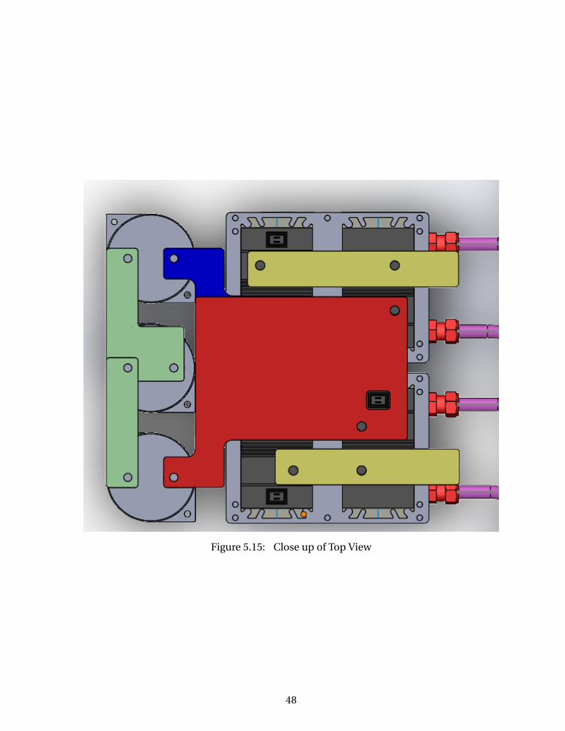
Figure 5.15: Close up of Top View
48

CHAPTER
6
CONCLUSION AND FUTURE WORK
A 6kV, 100A Virtual Full Power Test system is designed and verified in simulation for evalu-
ating switching characteristics of the Super Cascode Power Module.
6.1 Scope of future work
The test system hardware can be built from the proposed design and evaluated against
SCPM switching loss results obtained from Double Pulse Test method. A thermal description
model of the SCPM for PLECS simulation can be generated from monitoring SCPM base
plate temperature, switching loss and current during test.
49

Bibliography
[1] B. Gao et al. “6.0kV, 100A, 175kHz super cascode power module for medium voltage,high power applications”. In: 2018 IEEE Applied Power Electronics Conference andExposition (APEC). 2018, pp. 1288–1293.
[2] Zheng Chen. “Characterization and Modeling of High-Switching-Speed Behavior ofSiC Active Devices”. Masters Thesis. Virginia Polytechnic Institute and State Univer-sity, 2009.
[3] A. Marzoughi, R. Burgos, and D. Boroyevich. “Characterization and Performance Eval-uation of the State-of-the-Art 3.3 kV 30 A Full-SiC MOSFETs”. In: IEEE Transactionson Industry Applications 55.1 (2019), pp. 575–583.
[4] A. Marzoughi, R. Burgos, and D. Boroyevich. “Characterization and comparison oflatest generation 900-V and 1.2-kV SiC MOSFETs”. In: 2016 IEEE Energy ConversionCongress and Exposition (ECCE). 2016, pp. 1–8.
[5] A. Marzoughi et al. “Characterization and Evaluation of the State-of-the-Art 3.3-kV400-A SiC MOSFETs”. In: IEEE Transactions on Industrial Electronics 64.10 (2017),pp. 8247–8257.
[6] J. Brandelero et al. “A non-intrusive method for measuring switching losses of GaNpower transistors”. In: IECON 2013 - 39th Annual Conference of the IEEE IndustrialElectronics Society. 2013, pp. 246–251.
[7] B. Cougo, H. Schneider, and T. Meynard. “Accurate switching energy estimation ofwide bandgap devices used in converters for aircraft applications”. In: 2013 15thEuropean Conference on Power Electronics and Applications (EPE). 2013, pp. 1–10.
[8] D. C. Hopkins and D. W. Root. “Synthesis of a new class of converters that utilizeenergy recirculation”. In: Proceedings of 1994 Power Electronics Specialist Conference- PESC’94. Vol. 2. 1994, 1167–1172 vol.2.
[9] Christina Marie DiMarino. “High Temperature Characterization and Analysis of Sili-con Carbide (SiC) Power Semiconductor Transistors”. Masters Thesis. Virginia Poly-technic Institute and State University, 2014.
[10] C. Salcines, A. Kruglov, and I. Kallfass. “A Novel Characterization Technique to ExtractHigh Voltage - High Current IV Characteristics of Power MOSFETs from DynamicMeasurements”. In: 2018 IEEE 6th Workshop on Wide Bandgap Power Devices andApplications (WiPDA). 2018, pp. 1–6. DOI: 10.1109/WiPDA.2018.8569160.
[11] P. Ladoux et al. “Test bench for the characterisation of experimental low voltageIGCTs”. In: 2004 IEEE 35th Annual Power Electronics Specialists Conference (IEEE Cat.No.04CH37551). Vol. 4. 2004, 2937–2942 Vol.4.
50

[12] Silverio Alvarez e Hidalgo. “Characterisation of 3.3kV IGCTs for Medium Power Appli-cations”. Sept. 2005. URL: https://oatao.univ-toulouse.fr/7446/.
[13] Power MOSFET Basics - Understanding Voltage Ratings. AN851. VISHAY SILICONIX.2017. URL: https://www.mouser.com/pdfdocs/Vishay_AN861.pdf.
[14] Bo Gao. “Scalable Medium Voltage and High Voltage Super Cascode Power Modules”.PhD thesis. North Carolina State University, 2018.
[15] 37502 Technical Datasheet. 37502. Belden Wire & Cable. 2020. URL:https://catalog.belden.com/techdata/EN/37502_techdata.pdf.
[16] H. A. Wheeler. “Simple Inductance Formulas for Radio Coils”. In: Proceedings of theInstitute of Radio Engineers 16.10 (1928), pp. 1398–1400. DOI: 10.1109/JRPROC.1928.221309.
[17] D. C. Meeker. Finite Element Method Magnetics. Version 4.2 (28Feb2018 Build). URL:http://www.femm.info.
[18] LNK-P2X-16-220 Datasheet. ICAR. URL:https://www.icar.com/genera_scheda_lnk.php?codice=LNK-P2X-16-220&lang=en.
[19] Illinois Capacitor. Voltage Balancing Resistors. URL: https://www.illinois-capacitor.com/pdf/papers/voltage_balancing_resistors.pdf.
[20] Type MG Precision High Voltage Resistors. Caddock. URL: http://www.caddock.com/Online_catalog/Mrktg_Lit/TypeMG.pdf.
[21] Jr. Daniel W. Root. “SYNTHESIS OF SWITCH-MODE POWER ELECTRONIC CIRCUITSFOR ENERGY RECIRCULATION AND STORAGE”. Masters Thesis. Auburn University,Sept. 1993.
[22] Current Transducer IT 200-S ULTRASTAB. LEM. 2014. URL: https://www.lem.com/sites/default/files/products_datasheets/it_200-s_ultrastab.pdf.
[23] Cold-Plate-ATS-1001-DIY. R20619. Advanced Thermal Systems. 2019. URL: https://www.qats.com/DataSheet/Cold-Plate-ATS-CP-1001-DIY.
[24] Heat Exchanger. R111020. Advanced Thermal Systems. 2020. URL: https://www.qats.com/DataSheet/Heat-Exchangers.
[25] Technical Guide. Bulletin 0002-T1/USA. Parker Hannifin Corporation. 2003. URL:https://www.parker.com/Literature/Literature%5C%20Files/Partek/cat/english/TechBulletin.pdf.
[26] A. D. Callegaro et al. “Bus Bar Design for High-Power Inverters”. In: IEEE Transac-tions on Power Electronics 33.3 (2018), pp. 2354–2367. DOI: 10.1109/TPEL.2017.2691668.
51

[27] H. Gui et al. “Design of Low Inductance Busbar for 500 kVA Three-Level ANPCConverter”. In: 2019 IEEE Energy Conversion Congress and Exposition (ECCE). 2019,pp. 7130–7137. DOI: 10.1109/ECCE.2019.8912605.
[28] J. M. Guichon et al. “Busbar Design: How to Spare Nanohenries ?” In: ConferenceRecord of the 2006 IEEE Industry Applications Conference Forty-First IAS AnnualMeeting. Vol. 4. 2006, pp. 1865–1869. DOI: 10.1109/IAS.2006.256790.
[29] C. Chen et al. “Modeling and optimization of high power inverter three-layer lam-inated busbar”. In: 2012 IEEE Energy Conversion Congress and Exposition (ECCE).2012, pp. 1380–1385. DOI: 10.1109/ECCE.2012.6342654.
[30] Copper Development Association Inc. Ampacities and Mechanical Properties of Rect-angular Copper Busbars: Table 1. Ampacities of Copper No. 110. URL: https://www.copper.org/applications/electrical/busbar/bus_table1.html.
[31] J. M. Allocco. “Laminated bus bars for power system interconnects”. In: Proceedingsof APEC 97 - Applied Power Electronics Conference. Vol. 2. 1997, 585–589 vol.2. DOI:10.1109/APEC.1997.575624.
[32] Storm Power Components. Insulating Films. URL: https://stormpowercomponen-ts.com/insulation/insulating-films/.
52