L6 semiconductor-power-switching-devices-3-130912210901-phpapp01
23
Semiconductor Power Switching Devices-3 (Lecture-6) R S Ananda Murthy Associate Professor and Head Department of Electrical & Electronics Engineering, Sri Jayachamarajendra College of Engineering, Mysore 570 006 R S Ananda Murthy Semiconductor Power Switching Devices-3
-
Upload
neomindx -
Category
Engineering
-
view
28 -
download
0
Transcript of L6 semiconductor-power-switching-devices-3-130912210901-phpapp01

Semiconductor Power Switching Devices-3(Lecture-6)
R S Ananda Murthy
Associate Professor and HeadDepartment of Electrical & Electronics Engineering,
Sri Jayachamarajendra College of Engineering,Mysore 570 006
R S Ananda Murthy Semiconductor Power Switching Devices-3

TRIAC
MT2
MT1
G
Circuit Symbolof TRIAC
J1
J2
J3
Structure of TRIAC
+ indicates heavily doped region- indicates lightly doped region
MT1
MT2
G
J4ON
OFF
ON
OFF
MT2 positivew.r.t. MT1 andG positive w.r.t. MT1
Pulse triggered
MT2 negativew.r.t. MT1 andG negative w.r.t. MT1
Pulse triggered
MT1 MT2
GTRIAC is equivalent totwo SCRs in anti-parallel
Shorting of p1 region to n3 region due to MT2 metal contact,and the p2 region to the n2 region due to MT1 metal contactresults in two anti-parallel SCR structures: p1n1p2n2 andp2n1p1n3.
R S Ananda Murthy Semiconductor Power Switching Devices-3

TRIAC used in ACVC
VRMS
Constant
f
AC
ACVCV,
AC
Variable
same as inputf
(a)
vivo
(b)
Triac+
−
R
+
−
vi
vo
tω
tω
(c)
0
Trigger
0
Trigger Trigger
π 2π
π 2π
R S Ananda Murthy Semiconductor Power Switching Devices-3

Limitations of TRIAC as Compared to SCRs
Has lower dv/dt rating.Requires well designed R-C snubber connected across itto limit dv/dt .Has longer turn-off time.Has lower power handling capability.Typically used in small motor speed regulators,temperature control, illumination control, liquid levelcontrol, phase control circuits, power switches.Cannot be used in A.C. systems of frequency more than400 Hz.
R S Ananda Murthy Semiconductor Power Switching Devices-3

Specifications of TRIAC BT139
R S Ananda Murthy Semiconductor Power Switching Devices-3

Specifications of TRIAC BT139
R S Ananda Murthy Semiconductor Power Switching Devices-3

Specifications of TRIAC BT139
R S Ananda Murthy Semiconductor Power Switching Devices-3

Diac
MT1
MT2
P
N
P
J1
J2
MT1
MT2
MT1
MT2Structure and symbols of diac
Diacs are typically used to trigger TRIACS in ceiling fanregulators and light dimming circuits.
R S Ananda Murthy Semiconductor Power Switching Devices-3

Typical Diac Specifications
R S Ananda Murthy Semiconductor Power Switching Devices-3

Typical Diac Specifications
R S Ananda Murthy Semiconductor Power Switching Devices-3

Typical Diac Specifications
R S Ananda Murthy Semiconductor Power Switching Devices-3
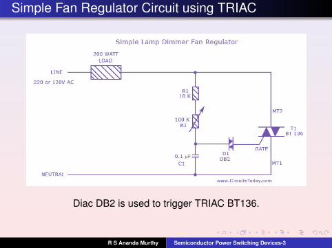
Simple Fan Regulator Circuit using TRIAC
Diac DB2 is used to trigger TRIAC BT136.
R S Ananda Murthy Semiconductor Power Switching Devices-3

Some High Power TRIACS
(Source: www.china-rectifier.com)
R S Ananda Murthy Semiconductor Power Switching Devices-3
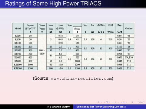
Ratings of Some High Power TRIACS
(Source: www.china-rectifier.com)
R S Ananda Murthy Semiconductor Power Switching Devices-3

Gate Turn Off Thyristor (GTO)
A
K
G
J1
J2J3
Buffer layer
A
K
G
Anode contact
Buffer layer structure Anode shorted structure
Anode short
A A
K K
GG
Circuit symbols of GTOIncreases reverse voltage
blocking capabilityDecreases reverse voltage
blocking capability
A
K
G
Inter digitized gate-cathode structure increases di/dt rating ofthe device and also improves turn-off performace of the device.
R S Ananda Murthy Semiconductor Power Switching Devices-3

Static Characteristic of GTO
A
KG
Circuit Symbolof GTO
ON
OFF
= Latching Current= Holding Current
ForwardLeakageCurrent
SymmetricalGTO
AsymmetricalGTO
R S Ananda Murthy Semiconductor Power Switching Devices-3

Control Characteristics of GTO
vo
iG
vo
+
−
iG
t
V
t
+
−
GTO
RV
GTO can be turned on by applying a positive gate currentpulse and turned off by applying a negative gate currentpulse.To prevent unwanted turn-off during transients, it isrecommended to apply a low value of continuous positivegate current as long as GTO has to be kept on.
R S Ananda Murthy Semiconductor Power Switching Devices-3

GTO Compared with SCR
GTO SCR
Fully-controlled Semi-controlled
VON = 3-4 V VON =1.5-2 V
Higher IL and IH IL and IH very low compared to GTO
Assymetric GTO has very low VBR Has VBR ≈ VBO
Typically dv/dt = 1000 V/µs Typically dv/dt =200-500 V/µs
Turn-off Current Gain: 6-15 Not applicable
Max. operating frequency: 1-4 kHz Typcally operated at 50 or 60 Hz
R S Ananda Murthy Semiconductor Power Switching Devices-3

Photographs of GTOs
Asymmetric Type Reverse Blocking Type
(Source: www.china-rectifier.com)
R S Ananda Murthy Semiconductor Power Switching Devices-3

Stud Type GTO
(Source: www.china-rectifier.com)
R S Ananda Murthy Semiconductor Power Switching Devices-3

Specifications of Asymmetric GTOs
(Source: www.china-rectifier.com)
R S Ananda Murthy Semiconductor Power Switching Devices-3

Specifications of Symmetric GTOs
(Source: www.china-rectifier.com)
R S Ananda Murthy Semiconductor Power Switching Devices-3

Next Lecture...
In the next lecture we will discuss some more powersemiconductor switching devices used in power electronics.
Thank You.
R S Ananda Murthy Semiconductor Power Switching Devices-3