Freescale Semiconductor MC33874 Advance Information Quad ...
38
Document Number: MC33874 Rev. 9.0, 8/2008 Freescale Semiconductor Advance Information * This document contains certain information on a new product. Specifications and information herein are subject to change without notice. © Freescale Semiconductor, Inc., 2006-2008. All rights reserved. Quad High Side Switch (Quad 35mΩ) The 33874 is one in a family of devices designed for low-voltage automotive and industrial lighting and motor control applications. Its four low R DS(ON) MOSFETs (four 35mΩ) can control the high sides of four separate resistive or inductive loads. Programming, control, and diagnostics are accomplished using a 16-bit SPI interface. Additionally, each output has its own parallel input for pulse-width modulation (PWM) control if desired. The 33874 allows the user to program via the SPI the fault current trip levels and duration of acceptable lamp inrush or motor stall intervals. Such programmability allows tight control of fault currents and can protect wiring harnesses and circuit boards as well as loads. The 33874 is packaged in a power-enhanced 12 x 12 nonleaded Power QFN package with exposed tabs. Features • Quad 35mΩ high side switches (at 25°C) • Operating voltage range of 6.0V to 27V with standby current < 5.0μA • SPI control of over-current limit, over-current fault blanking time, output OFF open load detection, output ON / OFF control, watchdog timeout, slew rates, and fault status reporting • SPI status reporting of over-current, open and shorted loads, over-temperature, under-voltage and over-voltage shutdown, fail-safe pin status, and program status • Analog current feedback with selectable ratio • Analog board temperature feedback • Enhanced -16V reverse polarity V PWR protection • Pb-free packaging designated by suffix code PNA Figure 1. 33874 Simplified Application Diagram HIGH SIDE SWITCH PNA SUFFIX (PB_FREE) 98ART10510D 24-PIN PQFN (12 x 12) 33874 ORDERING INFORMATION Device Temperature Range (T A ) Package MC33874BPNA/R2 - 40°C to 125°C 24 PQFN 33874 HS0 HS1 GND GND FSI CSNS HS2 HS3 MCU SCLK LOAD 0 LOAD 1 LOAD 2 LOAD 3 SCLK IN0 I/O IN1 IN2 IN3 I/O SI SO I/O I/O A/D VPWR VDD V DD V PWR WAKE I/O I/O V DD V DD CS CS RST SO V PWR SI FS TEMP A/D
Transcript of Freescale Semiconductor MC33874 Advance Information Quad ...

Document Number: MC33874Rev. 9.0, 8/2008
Freescale Semiconductor Advance Information
Quad High Side Switch (Quad 35mΩ)
The 33874 is one in a family of devices designed for low-voltage automotive and industrial lighting and motor control applications. Its four low RDS(ON) MOSFETs (four 35mΩ) can control the high sides of four separate resistive or inductive loads.
Programming, control, and diagnostics are accomplished using a 16-bit SPI interface. Additionally, each output has its own parallel input for pulse-width modulation (PWM) control if desired. The 33874 allows the user to program via the SPI the fault current trip levels and duration of acceptable lamp inrush or motor stall intervals. Such programmability allows tight control of fault currents and can protect wiring harnesses and circuit boards as well as loads.
The 33874 is packaged in a power-enhanced 12 x 12 nonleaded Power QFN package with exposed tabs.
Features• Quad 35mΩ high side switches (at 25°C)• Operating voltage range of 6.0V to 27V with standby current <
5.0μA• SPI control of over-current limit, over-current fault blanking time,
output OFF open load detection, output ON / OFF control, watchdog timeout, slew rates, and fault status reporting
• SPI status reporting of over-current, open and shorted loads, over-temperature, under-voltage and over-voltage shutdown, fail-safe pin status, and program status
• Analog current feedback with selectable ratio• Analog board temperature feedback• Enhanced -16V reverse polarity VPWR protection• Pb-free packaging designated by suffix code PNA
Figure 1. 33874 Simplified Application Diagram
HIGH SIDE SWITCH
PNA SUFFIX (PB_FREE)98ART10510D
24-PIN PQFN (12 x 12)
33874
ORDERING INFORMATION
Device Temperature Range (TA) Package
MC33874BPNA/R2 - 40°C to 125°C 24 PQFN
33874
HS0
HS1
GNDGND
FSI
CSNS
HS2
HS3
MCU
SCLK
LOAD 0
LOAD 1
LOAD 2
LOAD 3
SCLK
IN0I/O
IN1
IN2
IN3
I/O
SI SO
I/O
I/O
A/D
VPWRVDD
VDD
VPWR
WAKE
I/O
I/O
VDD
VDD
CSCS
RST
SO
VPWR
SI
FS
TEMPA/D
* This document contains certain information on a new product. Specifications and information herein are subject to change without notice.
© Freescale Semiconductor, Inc., 2006-2008. All rights reserved.

INTERNAL BLOCK DIAGRAM
INTERNAL BLOCK DIAGRAM
Figure 2. 33874 Simplified Internal Block Diagram
GND
ProgrammableWatchdog
279ms–2250ms
Over-temperatureDetection
Logic
SPI3.0MHz
Selectable Over-
HS[0:3]: 2.8A–10A
Selectable Over-current
Internal Regulator
Selectable SlewRate Gate Drive
Over/Under-voltageProtection
HS0
VPWRVDD
CSSCLK
SOSI
RSTWAKE
FSIN0
FSI
IN3
HS1
HS0
HS1
HS2
HS3
HS2
HS3
IN1IN2
current Low Detection
HS[0:3]: 55A or 40A
Selectable Output Current
HS[0:3]: 1/7200 or 1/21400
CSNS
Recopy (Analog MUX)
VIC
VIC
IDWN
IUP
IDWNRDWN
Open LoadDetection
High Detection
Selectable Over-current Low Detection
0.15ms–155msBlanking Time
Temperature FeedbackTEMP
VIC
Analog Integrated Circuit Device Data 2 Freescale Semiconductor
33874
PIN CONNECTIONS
PIN CONNECTIONS
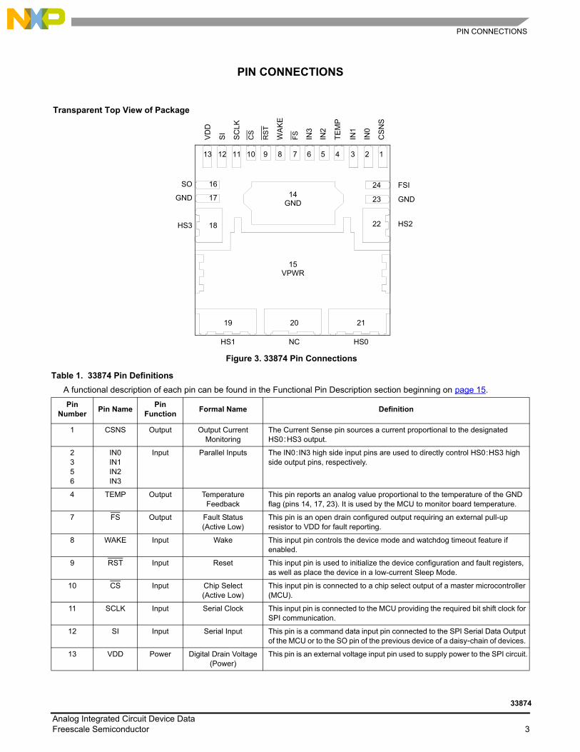
Figure 3. 33874 Pin Connections Table 1. 33874 Pin Definitions
A functional description of each pin can be found in the Functional Pin Description section beginning on page 15.
Pin Number Pin Name Pin
Function Formal Name Definition
1 CSNS Output Output Current Monitoring
The Current Sense pin sources a current proportional to the designated HS0 : HS3 output.
2356
IN0IN1IN2IN3
Input Parallel Inputs The IN0 : IN3 high side input pins are used to directly control HS0 : HS3 high side output pins, respectively.
4 TEMP Output Temperature Feedback
This pin reports an analog value proportional to the temperature of the GND flag (pins 14, 17, 23). It is used by the MCU to monitor board temperature.
7 FS Output Fault Status(Active Low)
This pin is an open drain configured output requiring an external pull-up resistor to VDD for fault reporting.
8 WAKE Input Wake This input pin controls the device mode and watchdog timeout feature if enabled.
9 RST Input Reset This input pin is used to initialize the device configuration and fault registers, as well as place the device in a low-current Sleep Mode.
10 CS Input Chip Select (Active Low)
This input pin is connected to a chip select output of a master microcontroller (MCU).
11 SCLK Input Serial Clock This input pin is connected to the MCU providing the required bit shift clock for SPI communication.
12 SI Input Serial Input This pin is a command data input pin connected to the SPI Serial Data Output of the MCU or to the SO pin of the previous device of a daisy-chain of devices.
13 VDD Power Digital Drain Voltage (Power)
This pin is an external voltage input pin used to supply power to the SPI circuit.
Transparent Top View of Package
13
24
12 10 9 8 7 6 5 4 3 2 111
23
22
19 20 21
16
17
18
15
14SO
GND
HS3
HS1 NC HS0
HS2
GND
FSI
VD
D
SI
SC
LK
CS
RS
T
WAK
E
FS IN3
IN2
TEM
P
IN1
IN0
CS
NS
GND
VPWR
Analog Integrated Circuit Device Data Freescale Semiconductor 3
33874

PIN CONNECTIONS
14, 17, 23 GND Ground Ground These pins are the ground for the logic and analog circuitry of the device.
15 VPWR Power Positive Power Supply This pin connects to the positive power supply and is the source of operational power for the device.
16 SO Output Serial Output This output pin is connected to the SPI Serial Data Input pin of the MCU or to the SI pin of the next device of a daisy-chain of devices.
18192122
HS3HS1HS0HS2
Output High Side Outputs Protected 35mΩ high side power output pins to the load.
20 NC N/A No Connect This pin may not be connected.
24 FSI Input Fail-safe Input The value of the resistance connected between this pin and ground determines the state of the outputs after a watchdog timeout occurs.
Table 1. 33874 Pin Definitions (continued)A functional description of each pin can be found in the Functional Pin Description section beginning on page 15.
Pin Number Pin Name Pin
Function Formal Name Definition
Analog Integrated Circuit Device Data 4 Freescale Semiconductor
33874

ELECTRICAL CHARACTERISTICSMAXIMUM RATINGS
ELECTRICAL CHARACTERISTICS
MAXIMUM RATINGS
Table 2. Maximum Ratings All voltages are with respect to ground unless otherwise noted. Exceeding these ratings may cause a malfunction or
permanent damage to the device.
Ratings Symbol Value Unit
ELECTRICAL RATINGS
Operating Voltage RangeSteady-State
VPWR(SS)-16 to 41
V
VDD Supply Voltage VDD -0.3 to 5.5 V
Input / Output Voltage(1) See note (1) - 0.3 to 7.0 V
SO Output Voltage(1) VSO - 0.3 to VDD + 0.3 V
WAKE Input Clamp Current ICL(WAKE) 2.5 mA
CSNS Input Clamp Current ICL(CSNS) 10 mA
HS [0:3] VoltagePositiveNegative
VHS41-16
V
Output Current(2) IHS[0:3] 11 A
Output Clamp Energy(3) ECL [0:3] 85 mJ
ESD Voltage(4)
Human Body Model (HBM) Charge Device Model (CDM)
Corner Pins (1, 13, 19, 21)All Other Pins (2-12, 14-18, 20, 22-24)
VESD ± 2000
± 750± 500
V
THERMAL RATINGS
Operating TemperatureAmbientJunction
TA
TJ
- 40 to 125- 40 to 150
°C
Storage Temperature TSTG - 55 to 150 °C
Thermal Resistance(5)
Junction to CaseJunction to Ambient
RθJCRθJA
<1.030
°C/ W
Peak Pin Reflow Temperature During Solder Mounting(6) TSOLDER Note 6 °C
Notes1. Exceeding voltage limits on IN[0:3], RST, FSI, CSNS, TEMP, SI, SO, SCLK, CS, or FS pins may cause a malfunction or permanent
damage to the device.2. Continuous high side output current rating so long as maximum junction temperature is not exceeded. Calculation of maximum output
current using package thermal resistance is required. 3. Active clamp energy using single-pulse method (L = 2mH, RL = 0Ω, VPWR = 14V, TJ = 150°C initial).
4. ESD testing is performed in accordance with the Human Body Model (CZAP = 100pF, RZAP = 1500Ω), Charge Device Model (CDM), Robotic (CZAP = 4.0pF).
5. Device mounted on a 2s2p test board per JEDEC JESD51-2.6. Freescale’s Package Reflow capability meets Sn-Pb-free requirements for JEDEC standard J-STD-020A. For Peak Package Reflow
Temperature and Moisture Sensitivity Levels (MSL), Go to www.freescale.com, search by part number [e.g. remove prefixes/suffixes and enter the core ID to view all orderable parts. (i.e. MC33xxxD enter 33xxx), and review parametrics.
Analog Integrated Circuit Device Data Freescale Semiconductor 5
33874

ELECTRICAL CHARACTERISTICSSTATIC ELECTRICAL CHARACTERISTICS
33874
STATIC ELECTRICAL CHARACTERISTICS
Table 3. Static Electrical Characteristics Characteristics noted under conditions 6.0V ≤ VPWR ≤ 27V, 4.5V ≤ VDD ≤ 5.5V, - 40°C ≤ TA ≤ 125°C, GND = 0V, unless
otherwise noted. Typical values noted reflect the approximate parameter means at TA = 25°C under nominal conditions, unless otherwise noted.
Characteristic Symbol Min Typ Max Unit
POWER INPUT (VPWR, VDD)
Battery Supply Voltage RangeFully Operational
VPWR6.0 – 27
V
VPWR Operating Supply Current Outputs ON, HS[0 : 3] open
IPWR(ON)– – 20
mA
VPWR Supply CurrentOutputs OFF, Open Load Detection Disabled, WAKE > 0.7 x VDD, RST = VLOGIC HIGH
IPWR(SBY)
– – 5.0
mA
Sleep State Supply Current (VPWR = 14V, RST < 0.5V, WAKE < 0.5V) TA = 25°CTA = 85°C
IPWR(SLEEP) ––
1.0–
1050
μA
VDD Supply Voltage VDD(ON) 4.5 5.0 5.5 V
VDD Supply CurrentNo SPI Communication3.0MHz SPI Communication(7)
IDD(ON)––
––
1.05.0
mA
VDD Sleep State Current IDDSLEEP – – 5.0 μA
Over-voltage Shutdown Threshold VOV 28 32 36 V
Over-voltage Shutdown Hysteresis VOVHYS 0.2 0.8 1.5 V
Under-voltage Shutdown Threshold(8) VUV 4.75 5.25 5.75 V
Under-voltage Hysteresis(9) VUVHYS – 0.25 – V
Under-voltage Power-ON Reset VUVPOR – – 4.75 V
Notes7. Not guaranteed in production.8. The under-voltage fault condition is reported to SPI register as long as the external VDD supply is within specification and the VPWR
voltage level does not go below the under-voltage Power-ON Reset threshold.9. This applies when the under-voltage fault is not latched (IN = [0:3]).
Analog Integrated Circuit Device Data 6 Freescale Semiconductor

ELECTRICAL CHARACTERISTICSSTATIC ELECTRICAL CHARACTERISTICS
OUTPUTS (HS0, HS1, HS2, HS3)
Output Drain-to-Source ON Resistance (IHS = 5.0A, TA = 25°C)VPWR = 6.0VVPWR = 10VVPWR = 13V
RDS(ON)–––
–––
553535
mΩ
Output Drain-to-Source ON Resistance (IHS = 5.0A, TA = 150°C)VPWR = 6.0VVPWR = 10V VPWR = 13V
RDS(ON)–––
–––
946060
mΩ
Output Source-to-Drain ON Resistance(10)
IHS = 1.0A, TA = 25°C, VPWR = -12VRSD(ON)
– – 70mΩ
Output Overcurrent High Detection Levels (9.0V < VPWR < 16V)SOCH = 0SOCH = 1
IOCH0IOCH1
4432
5540
6648
A
Overcurrent Low Detection Levels (9.0V < VPWR < 16V) SOCL[2:0] : 000 SOCL[2:0] : 001SOCL[2:0] : 010SOCL[2:0] : 011SOCL[2:0] : 100SOCL[2:0] : 101SOCL[2:0] : 110SOCL[2:0] : 111
IOCL0IOCL1IOCL2IOCL3IOCL4IOCL5IOCL6IOCL7
8.07.16.35.64.63.83.12.2
108.97.97.05.84.83.92.8
1210.79.58.57.05.84.73.4
A
Current Sense Ratio (9.0V < VPWR < 16V, CSNS < 4.5V)DICR D2 = 0 DICR D2 = 1
CSR0CSR1
––
1/72001/21400
––
–
Current Sense Ratio (CSR0) AccuracyOutput Current
2.0A to 10A
CSR0_ACC
-17 – 17
%
Notes10. Source-Drain ON Resistance (Reverse Drain-to-Source ON Resistance) with negative polarity VPWR.
Table 3. Static Electrical Characteristics (continued)Characteristics noted under conditions 6.0V ≤ VPWR ≤ 27V, 4.5V ≤ VDD ≤ 5.5V, - 40°C ≤ TA ≤ 125°C, GND = 0V, unless
otherwise noted. Typical values noted reflect the approximate parameter means at TA = 25°C under nominal conditions, unless otherwise noted.
Characteristic Symbol Min Typ Max Unit
Analog Integrated Circuit Device Data Freescale Semiconductor 7
33874

ELECTRICAL CHARACTERISTICSSTATIC ELECTRICAL CHARACTERISTICS
33874
OUTPUTS (HS0, HS1, HS2, HS3) (continued)
Current Sense Ratio (CSR1) AccuracyOutput Current
10A to 20A
CSR1_ACC
-19 – 19
%
Current Sense Clamp VoltageCSNS Open; IHS[0:3] = 11A
VCL(CSNS)4.5 6.0 7.0
V
Open Load Detection Current(11) IOLDC 30 – 100 μA
Output Fault Detection Threshold Output Programmed OFF
VOFD(THRES)2.0 3.0 4.0
V
Output Negative Clamp Voltage0.5A < IHS[0:3] < 2.0A, Output OFF
VCL
- 20 – -16V
Over-temperature Shutdown(12) TSD 155 175 190 °C
Over-temperature Shutdown Hysteresis(12) TSD(HYS) 5.0 – 20 °C
Notes11. Output OFF Open Load Detection Current is the current required to flow through the load for the purpose of detecting the existence of
an open load condition when the specific output is commanded OFF.12. Guaranteed by process monitoring. Not production tested.
Table 3. Static Electrical Characteristics (continued)Characteristics noted under conditions 6.0V ≤ VPWR ≤ 27V, 4.5V ≤ VDD ≤ 5.5V, - 40°C ≤ TA ≤ 125°C, GND = 0V, unless
otherwise noted. Typical values noted reflect the approximate parameter means at TA = 25°C under nominal conditions, unless otherwise noted.
Characteristic Symbol Min Typ Max Unit
Analog Integrated Circuit Device Data 8 Freescale Semiconductor

ELECTRICAL CHARACTERISTICSSTATIC ELECTRICAL CHARACTERISTICS
CONTROL INTERFACE (SCLK, SI, SO, IN[0:3], RST, WAKE, FS, CS, FSI)
Input Logic High-voltage(13) VIH 0.7 VDD – – V
Input Logic Low-voltage(13) VIL – – 0.2 VDD V
Input Logic Voltage Hysteresis(14) VIN(HYS) 100 850 1200 mV
Input Logic Pull-down Current (SCLK, SI, IN[0:3], VIN>0.2 x VDD) IDWN 5.0 – 20 μA
RST Input Voltage Range VRST 4.5 5.0 5.5 V
SO, FS Tri-State Capacitance(14) CSO – – 20 pF
Input Logic Pull-down Resistor (RST) and WAKE RDWN 100 200 400 kΩ
Input Capacitance(15) CIN – 4.0 12 pF
Wake Input Clamp Voltage(16)
ICL(WAKE) < 2.5mAVCL(WAKE)
7.0 – 14V
Wake Input Forward Voltage ICL(WAKE) = -2.5mA
VF(WAKE)- 2.0 – - 0.3
V
SO High-state Output VoltageIOH = 1.0mA
VSOH0.8 VDD – –
V
FS, SO Low-state Output VoltageIOL = -1.6mA
VSOL– 0.2 0.4
V
SO Tri-state Leakage CurrentCS > 0.7 x VDD, 0 < VSO < VDD
ISO(LEAK)- 5.0 0 5.0
μA
Input Logic Pull-up Current(17)
CS, VIN < 0.7 x VDD
IUP5.0 – 20
μA
FSI Input pin External Pull-down Resistance(18)
FSI Disabled, HS[0:3] state according to direct inputs state and SPI INx_SPI bits and A/O_s bitFSI Enabled, HS[0:3] OFFFSI Enabled, HS0 ON, HS[1:3] OFFFSI Enabled, HS0 and HS2 ON, HS1 and HS3 OFF
RFS
–6.01540
06.517
Infinite
1.07.019–
kΩ
Temperature FeedbackTA = 25°C
TFEED3.8 3.9 4.0
V
Temperature Feedback Derating DTFEED -7.2 -7.5 -7.8 mV/°C
Notes13. Upper and lower logic threshold voltage range applies to SI, CS, SCLK, RST, IN[0:3], and WAKE input signals. The WAKE and RST
signals may be supplied by a derived voltage referenced to VPWR.14. No hysteresis on FSI and wake pins. Parameter is guaranteed by process monitoring but is not production tested.15. Input capacitance of SI, CS, SCLK, RST, and WAKE. This parameter is guaranteed by process monitoring but is not production tested.16. The current must be limited by a series resistance when using voltages > 7.0V.17. Pull-up current is with CS OPEN. CS has an active internal pull-up to VDD.18. The selection of the RFS must take into consideration the tolerance, temperature coefficient and lifetime duration to assure that the
resistance value will always be within the desired (specified) range.
Table 3. Static Electrical Characteristics (continued)Characteristics noted under conditions 6.0V ≤ VPWR ≤ 27V, 4.5V ≤ VDD ≤ 5.5V, - 40°C ≤ TA ≤ 125°C, GND = 0V, unless
otherwise noted. Typical values noted reflect the approximate parameter means at TA = 25°C under nominal conditions, unless otherwise noted.
Characteristic Symbol Min Typ Max Unit
Analog Integrated Circuit Device Data Freescale Semiconductor 9
33874

ELECTRICAL CHARACTERISTICSDYNAMIC ELECTRICAL CHARACTERISTICS
33874
DYNAMIC ELECTRICAL CHARACTERISTICS
Table 4. Dynamic Electrical Characteristics
Characteristics noted under conditions 6.0V ≤ VPWR ≤ 27V, 4.5V ≤ VDD ≤ 5.5V, - 40°C ≤ TA ≤ 125°C, GND = 0V, unless otherwise noted. Typical values noted reflect the approximate parameter means at TA = 25°C under nominal conditions, unless otherwise noted.
Characteristic Symbol Min Typ Max Unit
POWER OUTPUT TIMING (HS0, HS1, HS2, HS3)
Output Rising Slow Slew Rate A (DICR D3 = 0)(19)
9.0V < VPWR < 16V SRRA_SLOW
0.1 0.3 0.75V/μs
Output Rising Slow Slew Rate B (DICR D3 = 0)(20)
9.0V < VPWR < 16VSRRB_SLOW
0.015 0.05 0.15V/μs
Output Rising Fast Slew Rate A (DICR D3 = 1)(19)
9.0V < VPWR < 16V SRRA_FAST
0.5 1.5 3.0V/μs
Output Rising Fast Slew Rate B (DICR D3 = 1)(20)
9.0V < VPWR < 16VSRRB_FAST
0.025 0.3 1.0V/μs
Output Falling Slow Slew Rate A (DICR D3 = 0)(19)
9.0V < VPWR < 16V SRFA_SLOW
0.1 0.3 0.75V/μs
Output Falling Slow Slew Rate B (DICR D3 = 0)(20)
9.0V < VPWR < 16V SRFB_SLOW
0.015 0.05 0.15V/μs
Output Falling Fast Slew Rate A (DICR D3 = 1)(19)
9.0V < VPWR < 16VSRFA_FAST
0.5 1.5 3.0V/μs
Output Falling Fast Slew Rate B (DICR D3 = 1)(20)
9.0V < VPWR < 16VSRFB_FAST
0.025 0.3 1.0V/μs
Output Turn-ON Delay Time in Slow Slew Rate(21)
DICR = 0t DLY_SLOW(ON)
2.0 30 200μs
Output Turn-ON Delay Time in Fast Slew Rate(21)
DICR = 1t DLY_FAST(ON)
1.0 6.0 100μs
Output Turn-OFF Delay Time in Slow Slew Rate Mode(22) DICR = 0
t DLY_SLOW(OFF) 40 200 800
μs
Output Turn-OFF Delay Time in Fast Slew Rate Mode(22) DICR = 1
t DLY_FAST(OFF)20 50 400
μs
Over-current Low Detection Blanking TimeOCLT[1:0]: 00OCLT[1:0]: 01(23)
OCLT[1:0]: 10OCLT[1:0]: 11
t OCL0t OCL1t OCL2t OCL3
108–
550.08
155–
750.15
202–
950.3
ms
Notes19. Rise and Fall Slew Rates A measured across a 5.0Ω resistive load at high side output = 0.5V to VPWR - 3.5V (see Figure 4, page 12).
These parameters are guaranteed by process monitoring.20. Rise and Fall Slew Rates B measured across a 5.0Ω resistive load at high side output = 0.5V to VPWR - 3.5V (see Figure 4). These
parameters are guaranteed by process monitoring.21. Turn-ON delay time measured from rising edge of any signal (IN[0 : 3], SCLK, CS) that would turn the output ON to VHS[0 : 3] = 0.5V with
RL = 5.0Ω resistive load.22. Turn-OFF delay time measured from falling edge of any signal (IN[0 : 3], SCLK, CS) that would turn the output OFF to VHS[0 : 3] = VPWR -
0.5V with RL = 5.0Ω resistive load.23. This logical bit is not defined. Do not use.
Analog Integrated Circuit Device Data 10 Freescale Semiconductor

ELECTRICAL CHARACTERISTICSDYNAMIC ELECTRICAL CHARACTERISTICS
POWER OUTPUT TIMING (HS0, HS1, HS2, HS3) (continued)
Over-current High Detection Blanking Time tOCH 1.0 5.0 20 μs
CS to CSNS Valid Time(24) t CNSVAL – – 10 μs
Watchdog Timeout(25)
WD[1:0] : 00WD[1:0] : 01WD[1:0] : 10WD[1:0] : 11
t WDTO0t WDTO1t WDTO2t WDTO3
446223
1800900
558279
22501125
725363
29251463
ms
Direct Input Switching Frequency (DICR D3 = 0) fPWM - 300 - Hz
SPI INTERFACE CHARACTERISTICS (RST, CS, SCLK, SI, SO)
Maximum Frequency of SPI Operation f SPI – – 3.0 MHz
Required Low-state Duration for RST(26) t WRST – 50 350 ns
Rising Edge of CS to Falling Edge of CS (Required Setup Time)(27) t CS – – 300 ns
Rising Edge of RST to Falling Edge of CS (Required Setup Time)(27) t ENBL – – 5.0 μs
Falling Edge of CS to Rising Edge of SCLK (Required Setup Time)(27) t LEAD – 50 167 ns
Required High-state Duration of SCLK (Required Setup Time)(27) t WSCLKh – – 167 ns
Required Low-state Duration of SCLK (Required Setup Time)(27) t WSCLKl – – 167 ns
Falling Edge of SCLK to Rising Edge of CS (Required Setup Time)(27) t LAG – 50 167 ns
SI to Falling Edge of SCLK (Required Setup Time)(28) t SI (SU) – 25 83 ns
Falling Edge of SCLK to SI (Required Setup Time)(28) t SI (HOLD) – 25 83 ns
SO Rise TimeCL = 200pF
t RSO– 25 50
ns
SO Fall Time CL = 200pF
t FSO– 25 50
ns
SI, CS, SCLK, Incoming Signal Rise Time(28) t RSI – – 50 ns
SI, CS, SCLK, Incoming Signal Fall Time(28) t FSI – – 50 ns
Time from Falling Edge of CS to SO Low-impedance(29) t SO(EN) – – 145 ns
Time from Rising Edge of CS to SO High-impedance(30) t SO(DIS) – 65 145 ns
Time from Rising Edge of SCLK to SO Data Valid(31) 0.2 VDD ≤ SO ≤ 0.8 x VDD, CL = 200pF
t VALID– 65 105
ns
Notes24. Time necessary for the CSNS to be with ±5% of the targeted value.25. Watchdog timeout delay measured from the rising edge of WAKE or RST from a sleep state condition, to output turn-ON with the output
driven OFF and FSI floating. The values shown are for WDR setting of [00]. The accuracy of t WDTO is consistent for all configured watchdog timeouts.
26. RST low duration measured with outputs enabled and going to OFF or disabled condition.27. Maximum setup time required for the 33874 is the minimum guaranteed time needed from the microcontroller.28. Rise and Fall time of incoming SI, CS, and SCLK signals suggested for design consideration to prevent the occurrence of double pulsing.29. Time required for output status data to be available for use at SO. 1.0kΩ on pull-up on CS.30. Time required for output status data to be terminated at SO. 1.0kΩ on pull-up on CS.31. Time required to obtain valid data out from SO following the rise of SCLK.
Table 4. Dynamic Electrical Characteristics (continued)Characteristics noted under conditions 6.0V ≤ VPWR ≤ 27V, 4.5V ≤ VDD ≤ 5.5V, - 40°C ≤ TA ≤ 125°C, GND = 0V, unless
otherwise noted. Typical values noted reflect the approximate parameter means at TA = 25°C under nominal conditions, unless otherwise noted.
Characteristic Symbol Min Typ Max Unit
Analog Integrated Circuit Device Data Freescale Semiconductor 11
33874

ELECTRICAL CHARACTERISTICSTIMING DIAGRAMS
TIMING DIAGRAMS
Figure 4. Output Slew Rate and Time Delays
Figure 5. Over-current Shutdown
t
VPWRVPWR - 0.5V
VPWR - 3V
0.5V
VPWR
PWR-0.5 V
PWR-3.5 V
0.5 V
tDLY_SLOW(OFF) & tDLY_FAST(OFF)
SRRB_SLOW & SRRB
SRFB_SLOW & SRFB_FAST
SRFA_SLOW & SRFA_FAST
SRRA_SLOW & SRRA_FAST
CS
tDLY(ON)
V
V
LoadCurrent
IOCHx
IOCLx
tOCLx
Time
tOCH
Analog Integrated Circuit Device Data 12 Freescale Semiconductor
33874

ELECTRICAL CHARACTERISTICSTIMING DIAGRAMS
Figure 6. Over-current Low and High Detection
Figure 7. Input Timing Switching Characteristics
IOCH0
t OCL0t OCL2t OCL3t OCH
Time
Load Current
IOCH1IOCL0
IOCL2
IOCL3IOCL4IOCL5IOCL6IOCL7
IOCL1
SI
RSTB
CSB
SCLK
Don’t Care Don’t Care Don’t CareValid Valid
VIH
VIL
VIH
VIH
VIH
VIL
VIL
VIL
TwRSTB
TleadTwSCLKh TrSI
Tlag
TSIsu TwSCLKl
TSI(hold)TfSI
0.7 VDD
0.2 VDD
0.7VDD
0.2VDD
0.2VDD
0.7VDD
0.7VDD
TCSBTENBL
RST
SCLK
SI
CS
0.2 VDD
tWRSTtENBL
0.2 VDD
tLEADtWSCLKh
tRSI
0.7 VDD0.2 VDD
0.7 VDD0.2 VDD
tSI(SU) tWSCLKltSI(HOLD)
tFSI
0.7 VDD
t CS
tLAG
VIH
VIH
VIL
VIL
VIH
VIL
VIH
VIH
Analog Integrated Circuit Device Data Freescale Semiconductor 13
33874

ELECTRICAL CHARACTERISTICSTIMING DIAGRAMS
Figure 8. SCLK Waveform and Valid SO Data Delay Time
SO
SO
SCLK VOH
VOL
VOH
VOL
VOH
VOL
TfSI
TdlyLH
TdlyHL
TVALID
TrSO
TfSO
3.5V 50%
TrSI
High-to-Low
1.0V
0.7 VDD 0.2VDD
0.2 VDD 0.7 VDD
Low-to-High
tRSI tFSI
0.7 VDD
SCLK
SO
SO
VOH
VOL
VOH
VOL
VOH
VOL
1.0 V
0.2 VDD
0.7 VDD
tRSO
tFSO
0.2 VDD
tSO(EN)
tSO(DIS)
3.5 V
Low to High
High to Low
tVALID
Analog Integrated Circuit Device Data 14 Freescale Semiconductor
33874

FUNCTIONAL DESCRIPTIONINTRODUCTION
FUNCTIONAL DESCRIPTION
INTRODUCTION
The 33874 is one in a family of devices designed for low-voltage automotive and industrial lighting and motor control applications. Its four low RDS(ON) MOSFETs (35mΩ) can control the high sides of four separate resistive or inductive loads.
Programming, control, and diagnostics are accomplished using a 16-bit SPI interface. Additionally, each output has its own parallel input for PWM control if desired. The 33874
allows the user to program via the SPI the fault current trip levels and duration of acceptable lamp inrush or motor stall intervals. Such programmability allows tight control of fault currents and can protect wiring harnesses and circuit boards as well as loads.
The 33874 is packaged in a power-enhanced 12 x 12 nonleaded PQFN package with exposed tabs.
FUNCTIONAL PIN DESCRIPTION
OUTPUT CURRENT MONITORING (CSNS)
The Current Sense pin sources a current proportional to the designated HS0 : HS3 output. That current is fed into a ground-referenced resistor and its voltage is monitored by an MCU's A/D. The output to be monitored is selected via the SPI. This pin can be tri-stated through the SPI.
SERIAL INPUTS (IN0, IN1, IN2, IN3)
The IN0 : IN3 high side input pins are used to directly control HS0 : HS3 high side output pins, respectively. A SPI register determines if each input is activated or if the input logic state is OR ed or AND ed with the SPI instruction. These pins are to be driven with 5.0V CMOS levels, and they have an active internal pull-down current source.
TEMPERATURE FEEDBACK (TEMP)
This pin reports an analog voltage value proportional to the temperature of the GND. It is used by the MCU to monitor board temperature.
FAULT STATUS (FS)
This pin is an open drain configured output requiring an external pull-up resistor to VDD for fault reporting. If a device fault condition is detected, this pin is active LOW. Specific device diagnostic faults are reported via the SPI SO pin.
WAKE
This input pin controls the device mode and watchdog timeout feature if enabled. An internal clamp protects this pin from high damaging voltages when the output is current limited with an external resistor. This input has a passive internal pull-down.
RESET (RST)
This input pin is used to initialize the device configuration and fault registers, as well as place the device in a low-current sleep mode. The pin also starts the watchdog timer
when transitioning from logic [0] to logic [1]. This pin should not be allowed to be logic [1] until VDD is in regulation. This pin has a passive internal pull-down.
CHIP SELECT (CS)
The CS pin enables communication with the master microcontroller (MCU). When this pin is in a logic [0] state, the device is capable of transferring information to, and receiving information from, the MCU. The 33874 latches in data from the Input Shift registers to the addressed registers on the rising edge of CS. The device transfers status information from the power output to the Shift register on the falling edge of CS. The SO output driver is enabled when CS is logic [0]. CS should transition from a logic [1] to a logic [0] state only when SCLK is a logic [0]. CS has an active internal pull-up, IUP.
SERIAL CLOCK (SCLK)
The SCLK pin clocks the internal shift registers of the 33874 device. The serial input (SI) pin accepts data into the input shift register on the falling edge of the SCLK signal while the serial output (SO) pin shifts data information out of the SO line driver on the rising edge of the SCLK signal. It is important the SCLK pin be in a logic low state whenever CS makes any transition. For this reason, it is recommended the SCLK pin be in a logic [0] whenever the device is not accessed (CS logic [1] state). SCLK has an active internal pull-down. When CS is logic [1], signals at the SCLK and SI pins are ignored and SO is tri-stated (high-impedance) (see Figure 9, page 18).
SERIAL INPUT (SI)
This is a serial interface (SI) command data input pin. Each SI bit is read on the falling edge of SCLK. A 16-bit stream of serial data is required on the SI pin, starting with D15 to D0. The internal registers of the 33874 are configured and controlled using a 5-bit addressing scheme described in Table 8, page 22. Register addressing and configuration are
Analog Integrated Circuit Device Data Freescale Semiconductor 15
33874

FUNCTIONAL DESCRIPTIONFUNCTIONAL PIN DESCRIPTION
described in Table 9, page 22. The SI input has an active internal pull-down, IDWN.
DIGITAL DRAIN VOLTAGE (VDD)
This pin is an external voltage input pin used to supply power to the SPI circuit. In the event VDD is lost, an internal supply provides power to a portion of the logic, ensuring limited functionality of the device.
GROUND (GND)
This pin is the ground for the device.
POSITIVE POWER SUPPLY (VPWR)
This pin connects to the positive power supply and is the source of operational power for the device. The VPWR contact is the backside surface mount tab of the package.
SERIAL OUTPUT (SO)
The SO data pin is a tri-stateable output from the shift register. The SO pin remains in a high-impedance state until
the CS pin is put into a logic [0] state. The SO data is capable of reporting the status of the output, the device configuration, and the state of the key inputs. The SO pin changes state on the rising edge of SCLK and reads out on the falling edge of SCLK. Fault and input status descriptions are provided in Table 16, page 26.
HIGH SIDE OUTPUTS (HS3, HS1, HS0, HS2)
Protected 35mΩ high side power output pins to the load.
FAIL-SAFE INPUT (FSI)
The value of the resistance connected between this pin and ground determines the state of the outputs after a watchdog timeout occurs. Depending on the resistance value, either all outputs are OFF or the output HSO only is ON. If the FSI pin is left to float up to a logic [1] level, then the outputs HS0 and HS2 will turn ON when in the Fail-safe state. When the FSI pin is connected to GND, the watchdog circuit and Fail-safe operation are disabled. This pin incorporates an active internal pull-up current source.
Analog Integrated Circuit Device Data 16 Freescale Semiconductor
33874

FUNCTIONAL DESCRIPTIONFUNCTIONAL INTERNAL BLOCK DESCRIPTION
FUNCTIONAL INTERNAL BLOCK DESCRIPTION
ANALOG CONTROL CIRCUITRY
The 33874 is designed to operate from 6.0V to 27V on the VPWR Pin. The VPWR Pin supplies power to all internal regulators, analog and logic circuit blocks. The VDD supply is used for setting communication threshold levels and supplying power to the SPI interface logic. This IC architecture provides a very low standby current. The analog circuitry provides for over-current and over-temperature protection as well as temperature warning features.
MCU INTERFACE AND OUTPUT CONTROL
The device is designed with 4 inputs for PWM Output driver control, if desired. MCU programming, control and
diagnostics are accomplished using the 16-bit SPI interface. Several parallel control and status lines are provided.
HIGH–SIDE DRIVERS: HS0 – HS3
The 33874 provides high side load drive capability for 4 outputs. The RDSON for the output MOSFETs is 35mΩ. The outputs are protected for over-current and over-temperature. The MOSFET gate drive can be slew rate controlled using the SPI interface. There is also an open load detection feature. A ratioed value of the MOSFET output current is available to the MCU.
The device allows for control of the 4 outputs through the SPI interface or by use of the parallel inputs, which allows for PWM capability.
MC33874 - Functional Block Diagram
Analog Control Circuitry
Analog Integrated Circuit Device Data Freescale Semiconductor 17
33874

FUNCTIONAL DEVICE OPERATIONOPERATIONAL MODES
FUNCTIONAL DEVICE OPERATION
SPI PROTOCOL DESCRIPTION
The SPI interface has a full duplex, three-wire synchronous data transfer with four I/O lines associated with it: Serial Input (SI), Serial Output (SO), Serial Clock (SCLK), and Chip Select (CS).
The SI / SO pins of the 33874 follow a first-in first-out (D15 to D0) protocol, with both input and output words transferring the most significant bit (MSB) first. All inputs are compatible with 5.0V CMOS logic levels.
Figure 9. Single 16-Bit Word SPI Communication
OPERATIONAL MODES
The 33874 has four operating modes: Sleep, Normal, Fault, and Fail-safe. Table 5 summarizes details contained in succeeding paragraphs.
SLEEP MODE
The Default mode of the 33874 is the Sleep Mode. This is the state of the device after first applying battery voltage (VPWR) prior to any I/O transitions. This is also the state of the device when the WAKE and RST are both logic [0]. In the Sleep Mode, the output and all unused internal circuitry, such as the internal 5.0V regulator, are off to minimize current draw. In addition, all SPI-configurable features of the device are as if set to logic [0]. The 33874 will transition to the Normal or Fail-safe operating modes based on the WAKE and RST inputs as defined in Table 5.
NORMAL MODE
The 33874 is in Normal Mode when: • VPWR and VDD are within the normal voltage range.• RST pin is logic [1].• No fault has occurred.
FAIL-SAFE MODE
FAIL-SAFE MODE AND WATCHDOG
If the FSI input is not grounded, the watchdog timeout detection is active when either the WAKE or RST input pin transitions from logic [0] to logic [1]. The WAKE input is capable of being pulled up to VPWR with a series of limiting
CSCSB
SI
SCLK
SO
D15 D1 D2 D3 D4 D5 D6 D7 D8 D9 D14 D13 D12 D11 D10
OD12
D0
OD13 OD14 OD15 OD6OD7OD8OD9OD10OD11 OD1 OD2 OD3 OD4OD5
1. RSTB is in a logic H state during the above operation. 2. DO, D1, D2, ... , and D15 relate to the most recent ordered entry of program data into the LUX IC
NOTES:
OD0
CS
device.
1. RST is a logic [1] state during the above operation.2. D15:D0 relate to the most recent ordered entry of data into the device.3. OD15:OD0 relate to the first 16 bits of ordered fault and status data out of the device.
Notes
Table 5. Fail-Safe Operation and Transitions to Other 33874 Modes
Mode FS Wake RST WDTO Comments
Sleep x 0 0 x Device is in Sleep mode. All outputs are OFF
Normal 1 x 1 No Normal mode. Watchdog is active if enabled.
Fault 0 1 1 No Device is currently in fault mode. The faulted output(s) is (are) OFF.
0 1 00 0 1
Fail-Safe
1 0 1
Yes
Watchdog has timed out and the device is in Fail-safe Mode. The outputs are as configured with the RFS resistor connected to FSI. RST and WAKE must go from logic [1] to logic [0] simultaneously to bring the device out of the Fail-safe mode or momentarily tied the FSI pin to ground.
1 1 11 1 0
x = Don’t care.
Analog Integrated Circuit Device Data 18 Freescale Semiconductor
33874

FUNCTIONAL DEVICE OPERATIONPROTECTION AND DIAGNOSTIC FEATURES
resistance limiting the internal clamp current according to the specification.
The Watchdog timeout is a multiple of an internal oscillator and is specified in the Table 15, page 24. As long as the WD bit (D15) of an incoming SPI message is toggled within the minimum watchdog timeout period (WDTO), based on the programmed value of the WDR, the device will operate normally. If an internal watchdog timeout occurs before the WD bit, the device will revert to a Fail-safe mode until the device is reinitialized.
During the Fail-safe Mode, the outputs will be ON or OFF depending upon the resistor RFS connected to the FSI pin, regardless of the state of the various direct inputs and modes (Table 6).
In the Fail-safe Mode, the SPI register content is retained except for over-current high and low detection levels, timing and latched over-temperature which are reset to their default value (SOCL, SOCH, and OCTL and OT_latch_[0:3] bits). Then the watchdog, over-voltage, over-temperature, and over-current circuitry (with default value) are fully operational.
The Fail-safe Mode can be detected by monitoring the WDTO bit D2 of the WD register. This bit is logic [1] when the device is in Fail-safe Mode. The device can be brought out of the Fail-safe Mode by transitioning the WAKE and RST pins from logic [1] to logic [0] or forcing the FSI pin to logic [0].
Table 5 summarizes the various methods for resetting the device from the latched Fail-safe Mode.
If the FSI pin is tied to GND, the Watchdog fail-safe operation is disabled.
LOSS OF VDD
If the external 5.0 V supply is not within specification, or even disconnected, all register content is reset. The outputs can still be driven by the direct inputs IN0 : IN3. The 33874 uses the battery input to power the output MOSFET-related current sense circuitry and any other internal logic providing fail-safe device operation with no VDD supplied. In this state, the watchdog, under-voltage, over-voltage, over-temperature (latched) and over-current circuitry are fully operational with default values.
FAULT MODE
This 33874 indicates the faults below as they occur by driving the FS pin to logic [0]:
• Over-temperature fault• Over-voltage and under-voltage fault• Open load fault• Over-current fault (high and low)
The FS pin will automatically return to logic [1] when the fault condition is removed, except for overcurrent, overtemperature (in case of latching configuration) and in some cases of undervoltage.
The FS pin reports all faults. For latched faults, this pin is reset by a new Switch ON command (via the SPI or direct input IN).
Fault information is retained in the fault register and is available (and reset) via the SO pin during the first valid SPI communication (refer to Table 17, page 26).
PROTECTION AND DIAGNOSTIC FEATURES
OVER-TEMPERATURE FAULT (LATCHING OR NON-LATCHING)
The 33874 incorporates over-temperature detection and shutdown circuitry for each output structure.
The over-temperature is latched per default and can be unlatched through SPI with OT_latch_[0:3] bits.
An over-temperature fault condition results in turning OFF the corresponding output. To remove the fault and be able to turn ON again the outputs, the failure must be removed and:• in Normal Mode: the corresponding output must be
commanded OFF and ON again in case of over-temperature latched (OT_latch bit = 0).
• in Normal Mode: the corresponding output turns ON automatically if the temperature is below TSD-TSD(HYS) in case of unlatched over-temperature (OT_latch bit = 1).
• in Fail-safe Mode: the FSI input must be grounded and then set to its nominal voltage to switch ON the outputs.
The over-temperature fault (one for each output) is reported by SPI. If the over-temperature is latched, the SPI reports OTF_s = [1] and OCLF_s = [1]. In case of non-latched, OTF_s = [1] only is reported.
The fault bits will be cleared in the status register after either a valid SPI read command or a power on reset of the device.
OVERCURRENT FAULT (LATCHING)
The 33874 has eight programmable over-current low detection levels (IOCL) and two programmable over-current high detection levels (IOCH) for maximum device protection. The two selectable, simultaneously active over-current
Table 6. Output State During Fail-safe Mode
RFS (kΩ) High Side State
0 (shorted to ground) Fail-safe Mode Disabled
6.0 All HS OFF
15 HS0 ONHS1 : HS3 OFF
30 (open) HS0 and HS2 ON HS1 and HS3 OFF
Analog Integrated Circuit Device Data Freescale Semiconductor 19
33874

FUNCTIONAL DEVICE OPERATIONPROTECTION AND DIAGNOSTIC FEATURES
detection levels, defined by IOCH and IOCL, are illustrated in Figure 6, page 13. The eight different over-current low detect levels (IOCL0 : IOCL7) are illustrated in Figure 6.
If the load current level ever reaches the selected over-current low detection level and the over-current condition exceeds the programmed over-current time period (tOCx), the device will latch the output OFF.
If at any time the current reaches the selected IOCH level, then the device will immediately latch the fault and turn OFF the output, regardless of the selected tOCH driver.
For both cases, the device output will stay off indefinitely until the device is commanded OFF and then ON again.
OVER-VOLTAGE FAULT (NON-LATCHING)
The 33874 shuts down the output during an over-voltage fault (OVF) condition on the VPWR pin. The output remains in the OFF state until the over-voltage condition is removed. When experiencing this fault, the OVF fault bit is set in the bit D1 and cleared after either a valid SPI read or a power reset of the device.
The over-voltage protection can be disabled through SPI (bit OV_DIS). When disabled, the returned SO bit OD13 still reflects any over-voltage condition (over-voltage warning).
UNDER-VOLTAGE SHUTDOWN (LATCHING OR NON-LATCHING)
The output(s) will latch off at some battery voltage below 6.0 V. As long as the VDD level stays within the normal specified range, the internal logic states within the device will be sustained.
In the case where battery voltage drops below the under-voltage threshold (VPWRUV) output will turn off, FS will go to logic 0, and the fault register UVF bit will be set to 1.
Two cases need to be considered when the battery level recovers :
• If outputs command are low, FS will go to logic 1 but the UVF bit will remain set to 1 until the next read operation (warning report).
• If the output command is ON, then FS will remain at logic 0. The output must be turned OFF and ON again to re-enable the state of output and release FS. The UVF bit will remain set to 1 until the next read operation.
The under-voltage protection can be disabled through SPI (bit UV_dis = 1). In this case, the FS does not report any under-voltage fault condition, UVF bit is set to 1, and the output state is not changed as long as the battery voltage does not drop any lower than 2.5 V.
The daisy chain feature is available under VDD in nominal conditions.
Analog Integrated Circuit Device Data 20 Freescale Semiconductor
33874

FUNCTIONAL DEVICE OPERATIONPROTECTION AND DIAGNOSTIC FEATURES
OPEN LOAD FAULT (NON-LATCHING)
The 33874 incorporates open load detection circuitry on the output. Output open load fault (OLF) is detected and reported as a fault condition when the output is disabled (OFF). The open load fault is detected and latched into the status register after the internal gate voltage is pulled low enough to turn OFF the output. The OLF fault bit is set in the status register. If the open load fault is removed, the status register will be cleared after reading the register.
The open load protection can be disabled through SPI (bit OL_DIS). It is recommended to disable open load circuitry in case of a permanent disconnected load.
REVERSE BATTERY
The output survives the application of reverse voltage as low as -16V. Under these conditions, the output’s gate is
enhanced to keep the junction temperature less than 150°C. The ON resistance of the output is fairly similar to that in the Normal mode. No additional passive components are required except on VDD.
GROUND DISCONNECT PROTECTION
In the event the 33874 ground is disconnected from load ground, the device protects itself and safely turns OFF the output regardless of the state of the output at the time of disconnection. A 10KΩ resistor needs to be added between the wake pin and the rest of the circuitry in order to ensure that the device turns off in case of ground disconnect and to prevent this pin to exceed its maximum ratings.
Current limit resistors in the digital input lines protect the digital supply against excessive current (10kΩ typical).
Table 7. Device behavior in case of Under-voltage
Quad High Side Switch
(VPWR Battery Voltage) ∗∗
StateUV EnableIN[0:3] = 0
(Falling VPWR)
UV EnableIN[0:3] = 0
(Rising VPWR)
UV EnableIN_x*** = 1
(Falling VPWR)
UV EnableIN_x*** = 1
(Rising VPWR)
UV DisableIN[0:3] = 0(Falling or
Rising VPWR)
UV DisableIN_x*** = 1(Falling or
Rising VPWR)
VPWR > VPWRUV Output State OFF OFF ON OFF OFF ON
FS State 1 1 1 0 1 1
SPI Fault Register UVF Bit
0 1 until next read 0 1 0 (falling)1 until nextread (rising)
0 (falling)1 until nextread (rising)
VPWRUV > VPWR > UVPOR
Output State OFF OFF OFF OFF OFF ON
FS State 0 0 0 0 1 1
SPI Fault Register UVF Bit
1 1 1 1 1 1
UVPOR > VPWR > 2.5V ∗
Output State OFF OFF OFF OFF OFF ON
FS State 1 1 1 1 1 1
SPI Fault Register UVF Bit
1 until next read 1 until next read 1 until next read 1 until next read 1 until next read 1 until next read
2.5V > VPWR > 0V Output State OFF OFF OFF OFF OFF OFF
FS State 1 1 1 1 1 1
SPI Fault Register UVF Bit
1 until next read 1 until next read 1 until next read 1 until next read 1 until next read 1 until next read
Comments UV fault isnot latched
UV fault isnot latched
UV faultis latched
∗ = Typical value; not guaranteed ∗∗ = While VDD remains within specified range.*** = IN_x is equivalent to IN_x direct input or IN_spi_s SPI input.
Analog Integrated Circuit Device Data Freescale Semiconductor 21
33874

FUNCTIONAL DEVICE OPERATIONLOGIC COMMANDS AND REGISTERS
LOGIC COMMANDS AND REGISTERS
SERIAL INPUT COMMUNICATION
SPI communication is accomplished using 16-bit messages. A message is transmitted by the MCU starting with the MSB D15 and ending with the LSB, D0 (Table 8). Each incoming command message on the SI pin can be interpreted using the following bit assignments: the MSB, D15, is the watchdog bit. In some cases, output selection is done with bits D12 : D11. The next three bits, D10 : D8, are used to select the command register. The remaining five bits,
D4 : D0, are used to configure and control the outputs and their protection features.
Multiple messages can be transmitted in succession to accommodate those applications where daisy-chaining is desirable, or to confirm transmitted data, as long as the messages are all multiples of 16 bits. Any attempt made to latch in a message that is not 16 bits will be ignored.
The 33874 has defined registers, which are used to configure the device and to control the state of the outputs. Table 9, page 22, summarizes the SI registers.
DEVICE REGISTER ADDRESSING
The following section describes the possible register addresses and their impact on device operation.
ADDRESS 00000 — STATUS REGISTER (STATR_S)
The STATR register is used to read the device status and the various configuration register contents without disrupting the device operation or the register contents. The register bits D[4:0] determine the content of the first sixteen bits of SO data. In addition to the device status, this feature provides the ability to read the content of the OCR0, OCR1, SOCHLR,
Table 8. SI Message Bit Assignment
Bit Sig SI Msg Bit Message Bit Description
MSB D15 Watchdog in: toggled to satisfy watchdog requirements.
D14 : D15 Not used.
D12 : D11 Register address bits used in some cases for output selection.
D10 : D8 Register address bits.
D7 : D5 Not used.
D4 : D1 Used to configure the inputs, outputs, and the device protection features and SO status content.
LSB D0 Used to configure the inputs, outputs, and the device protection features and SO status content.
Table 9. Serial Input Address and Configuration Bit Map
SI RegisterSI Data
D15 D14 D13 D12 D11 D10 D9 D8 D7 D6 D5 D4 D3 D2 D1 D0
STATR_s WDIN 0 0 0 0 0 0 0 0 0 0 SOA4 SOA3 SOA2 SOA1 SOA0
OCR0 WDIN 0 0 0 0 0 0 1 0 0 0 0 IN3_SPI IN2_SPI IN1_SPI IN0_SPI
OCR1 WDIN 0 0 0 1 0 0 1 0 0 0 0 CSNS3 EN CSNS2 EN CSNS1 EN CSNS0 EN
SOCHLR_s WDIN 0 0 A1 A0 0 1 0 0 0 0 0 SOCH_s SOCL2_s SOCL1_s SOCL0_s
CDTOLR_s WDIN 0 0 A1 A0 0 1 1 0 0 0 0 OL_DIS_s OCL_DIS_s OCLT1_s OCLT0_s
DICR_s WDIN 0 0 A1 A0 1 0 0 0 0 0 0 FAST_SR_s CSNS_high_s DIR_DIS_s A/O_s
UOVR WDIN 0 0 0 0 1 0 1 0 0 0 0 OT_latch-1 OT_latch_0 UV_DIS OV_DIS
WDR WDIN 0 0 0 1 1 0 1 0 0 0 0 OT_latch_3 OT_latch_2 WD1 WD0
NAR WDIN 0 0 0 0 1 1 0 0 0 0 0 No Action (Allow Toggling of D15- WDIN)
RESET 0 0 0 X X X X X 0 0 0 0 0 0 0 0
x = Don’t care. s = Output selection with the bits A1A0 as defined in Table 10.D15 is used to toggle watchdog event (WDIN)
Analog Integrated Circuit Device Data 22 Freescale Semiconductor
33874

FUNCTIONAL DEVICE OPERATIONLOGIC COMMANDS AND REGISTERS
CDTOLR, DICR, UOVR, WDR, and NAR registers. (Refer to the section entitled Serial Output Communication (Device Status Return Data) beginning on page 24.)
ADDRESS 00001— OUTPUT CONTROL REGISTER (OCR0)
The OCR0 register allows the MCU to control the ON / OFF state of four outputs through the SPI. Incoming message bit D3 : D0 reflects the desired states of the four high side outputs (INx_SPI), respectively. A logic [1] enables the corresponding output switch and a logic [0] turns it OFF.
ADDRESS 01001— OUTPUT CONTROL REGISTER (OCR1)
Incoming message bits D3 : D0 reflect the desired output that will be mirrored on the Current Sense (CSNS) pin. A logic [1] on message bits D3 : D0 enables the CSNS pin for outputs HS3 : HS0, respectively. In the event the current sense is enabled for multiple outputs, the current will be summed. In the event that bits D3 : D0 are all logic [0], the output CSNS will be tri-stated. This is useful when several CSNS pins of several devices share the same A /D converter.
ADDRESS A1A0010 — SELECT OVER-CURRENT HIGH AND LOW REGISTER (SOCHLR_S)
The SOCHLR_s register allows the MCU to configure the output over-current low and high detection levels, respectively. Each output “s” is independently selected for configuration based on the state of the D12 : D11 bits (Table 10).
Each output can be configured to different levels. In addition to protecting the device, this slow blow fuse emulation feature can be used to optimize the load requirements matching system characteristics. Bits D2 : D0 set the over-current low detection level to one of eight possible levels, as shown in Table 11, page 23. Bit D3 sets the over-current high detection level to one of two levels, as outlined in Table 12, page 23.
ADDRESS A1A0011 — CURRENT DETECTION TIME AND OPEN LOAD REGISTER (CDTOLR)
The CDTOLR register is used by the MCU to determine the amount of time the device will allow an over-current low condition before an output latches OFF. Each output is independently selected for configuration based on A1A0 , which are the state of the D12 : D11 bits (refer to Table 10, page 23).
Bits D1 : D0 (OCLT1_s : OCLT0_s) allow the MCU to select one of three over-current fault blanking times defined in Table 13. Note that these timeouts apply only to the over-current low detection levels. If the selected over-current high level is reached, the device will latch off within 20μs.
Table 10. Output Selection
A1 (D12) A0 (D11) HS_s
0 0 HS0
0 1 HS1
1 0 HS2
1 1 HS3
Table 11. Over-current Low Detection Levels
SOCL2_s* (D2)
SOCL1_s* (D1)
SOCL0_s* (D0)
Over-current Low Detection (Amperes)
HS0 to HS3
0 0 0 10
0 0 1 8.9
0 1 0 7.9
0 1 1 7.0
1 0 0 5.8
1 0 1 4.8
1 1 0 3.9
1 1 1 2.8
* “_s” refers to the output, which is selected through bits D12 : D11; refer to Table 10, page 23.
Table 12. Over-current High Detection Levels
SOCH_s* (D3)Over-current High Detection (Amperes)
HS0 to HS3
0 55
1 40
* “_s” refers to the output, which is selected through bits D12 : D11; refer to Table 10, page 23.
Table 13. Over-current Low Detection Blanking Time
OCLT[1:0]_s* Timing
00 155ms
01 Do not use
10 75ms
11 150μs
* “_s” refers to the output, which is selected through bits D12 : D11; refer to Table 10, page 23.
Analog Integrated Circuit Device Data Freescale Semiconductor 23
33874

FUNCTIONAL DEVICE OPERATIONLOGIC COMMANDS AND REGISTERS
A logic [1] on bit D2 (OCL_DIS_s) disables the over-current low detection feature. When disabled, there is no timeout for the selected output and the over-current low detection feature is disabled.
A logic [1] on bit D3 (OL_DIS_s) disables the open load (OL) detection feature for the output corresponding to the state of bits D12 : D11.
ADDRESS A1A0100 — DIRECT INPUT CONTROL REGISTER (DICR)
The DICR register is used by the MCU to enable, disable, or configure the direct IN pin control of each output. Each output is independently selected for configuration based on the state bits D12 : D11 (refer to Table 10, page 23).
For the selected output, a logic [0] on bit D1 (DIR_DIS_s) will enable the output for direct control. A logic [1] on bit D1 will disable the output from direct control.
While addressing this register, if the Input was enabled for direct control, a logic [1] for the D0 (A/O_s) bit will result in a Boolean AND of the IN pin with its corresponding IN_SPI D[4:0] message bit when addressing OCR0. Similarly, a logic [0] on the D0 pin results in a Boolean OR of the IN pin to the corresponding message bits when addressing the OCR0. This register is especially useful if several loads are required to be independently PWM controlled. For example, the IN pins of several devices can be configured to operate all of the outputs with one PWM output from the MCU. If each output is then configured to be Boolean ANDed to its respective IN pin, each output can be individually turned OFF by SPI while controlling all of the outputs, commanded on with the single PWM output.
A logic [1] on bit D2 (CSNS_high_s) is used to select the high ratio on the CSNS pin for the selected output. The default value [0] is used to select the low ratio (Table 14).
A logic [1] on bit D3 (FAST_SR_s) is used to select the high speed slew rate for the selected output, the default value [0] corresponds to the low speed slew rate.
ADDRESS 00101 — UNDER-VOLTAGE / OVER-VOLTAGE AND HS[0,1] OVER-TEMPERATURE REGISTER (UOVR)
The UOVR register disables the under-voltage (D1) and/or over-voltage (D0) protection. When these two bits are [0], the under and over-voltages are active (default value).
The UOVR register allows the over-temperature detection latching on the HS0 and HS1. To latch the over-temperature, the bits (OT_latch_1 and OT_latch_0) must be set to [0] which is the default value. To disable the latching, both bits must be set to [1].
ADDRESS 01101 — WATCHDOG AND HS[2,3] OVER-TEMPERATURE REGISTER (WDR)
The WDR register is used by the MCU to configure the watchdog timeout. The watchdog timeout is configured using bits D1 and D0. When D1 and D0 bits are programmed for the desired watchdog timeout period (Table 15), the WDSPI bit should be toggled as well, ensuring the new timeout period is programmed at the beginning of a new count sequence.
The WDR register allows the over-temperature detection latching on the HS2 and HS3. To latch the over-temperature, the bits (OT_latch_3 and OT_latch_2) must be set to [0] which is the default value. To disable the latching, both bits must be set to [1].
ADDRESS 00110 — NO ACTION REGISTER (NAR)
The NAR register can be used to no-operation fill SPI data packets in a daisy-chain SPI configuration. This would allow devices to be unaffected by commands being clocked over a daisy-chained SPI configuration. By toggling the WD bit (D15) the watchdog circuitry would continue to be reset while no programming or data read back functions are being requested from the device.
SERIAL OUTPUT COMMUNICATION (DEVICE STATUS RETURN DATA)
When the CS pin is pulled low, the output register is loaded. Meanwhile, the data is clocked out MSB- (OD15-) first as the new message data is clocked into the SI pin. The first sixteen bits of data clocking out of the SO, and following a CS transition, is dependent upon the previously written SPI word.
Table 14. Current Sense Ratio
CSNS_high_s* (D2)Current Sense Ratio
HS0 to HS3
0 1/7200
1 1/21400
* “_s” refers to the output, which is selected through bits D12 : D11; refer to Table 10, page 23.
Table 15. Watchdog Timeout
WD[1:0] (D1, D0) Timing (ms)
00 558
01 279
10 2250
11 1125
Analog Integrated Circuit Device Data 24 Freescale Semiconductor
33874

FUNCTIONAL DEVICE OPERATIONLOGIC COMMANDS AND REGISTERS
Any bits clocked out of the Serial Output (SO) pin after the first 16 bits will be representative of the initial message bits clocked into the SI pin since the CS pin first transitioned to a logic [0]. This feature is useful for daisy-chaining devices as well as message verification.
A valid message length is determined following a CS transition of [0] to [1]. If there is a valid message length, the data is latched into the appropriate registers. A valid message length is a multiple of 16 bits. At this time, the SO pin is tri-stated and the fault status register is now able to accept new fault status information.
SO data will represent information ranging from fault status to register contents, user selected by writing to the STATR bits OD4, OD3, OD2, OD1, and OD0. The value of the previous bits SOA4 and SOA3 will determine which output the SO information applies to for the registers which are output specific; viz., Fault, SOCHLR, CDTOLR, and DICR registers.
Note that the SO data will continue to reflect the information for each output (depending on the previous OD4, OD3 state) that was selected during the most recent STATR write until changed with an updated STATR write.
The output status register correctly reflects the status of the STATR-selected register data at the time that the CS is pulled to a logic [0] during SPI communication, and/or for the period of time since the last valid SPI communication, with the following exceptions:
• The previous SPI communication was determined to be invalid. In this case, the status will be reported as though the invalid SPI communication never occurred.
• Battery transients below 6.0V resulting in an under-voltage shutdown of the outputs may result in incorrect data loaded into the status register. The SO data transmitted to the MCU during the first SPI communication following an under-voltage VPWR condition should be ignored.
• The RST pin transition from a logic [0] to [1] while the WAKE pin is at logic [0] may result in incorrect data loaded into the Status register. The SO data transmitted to the MCU during the first SPI communication following this condition should be ignored.
SERIAL OUTPUT BIT ASSIGNMENT
The 16 bits of serial output data depend on the previous serial input message, as explained in the following paragraphs. Table 16, page 26, summarizes SO returned data for bits OD15 : OD0.
• Bit OD15 is the MSB; it reflects the state of the watchdog bit from the previously clocked-in message.
• Bit OD14 remains logic [0] except when an under-voltage condition occurred.
• Bit OD13 remains logic [0] except when an over-voltage condition occurred.
• Bits OD12 : OD8 reflect the state of the bits SOA4 : SOA0 from the previously clocked in message.
• Bits OD7 : OD4 give the fault status flag of the outputs HS3 : HS0, respectively.
• The contents of bits OD3 : OD0 depend on bits D4 : D0 from the most recent STATR command SOA4 : SOA0 as explained in the paragraphs following Table 16.
Analog Integrated Circuit Device Data Freescale Semiconductor 25
33874

FUNCTIONAL DEVICE OPERATIONLOGIC COMMANDS AND REGISTERS
PREVIOUS ADDRESS SOA4 : SOA0 = A1A0000
Bits OD3 : OD0 reflect the current state of the Fault register (FLTR) corresponding to the output previously selected with the bits A1A0 (Table 17).
Note The FS pin reports all faults. For latched faults, this pin is reset by a new Switch OFF command (via SPI or direct input IN).
PREVIOUS ADDRESS SOA4 : SOA0 = 00001
Data in bits OD3 : OD0 contains IN3_SPI : IN0_SPI programmed bits for outputs HS3 : HS0, respectively.
PREVIOUS ADDRESS SOA4 : SOA0 = 01001
Data in bits OD3 : OD0 contains the programmed CSNS3 EN : CSNS0 EN bits for outputs HS3 : HS0, respectively.
PREVIOUS ADDRESS SOA4 : SOA0 = A1A0010
Data returned in bits OD3 : OD0 are programmed current values for the over-current high detection level (refer to Table 12, page 23) and the over-current low detection level (refer to Table 11, page 23), corresponding to the output previously selected with A1A0.
PREVIOUS ADDRESS SOA4 : SOA0= A1A0011
The returned data contains the programmed values in the CDTOLR register for the output selected with A1A0.
PREVIOUS ADDRESS SOA4 : SOA0 = A1A0100
The returned data contains the programmed values in the DICR register for the output selected with A1A0.
PREVIOUS ADDRESS SOA4 : SOA0 = 00101
The returned data contains the programmed values in the UOVR register.
PREVIOUS ADDRESS SOA4 : SOA0 = 01101
The returned data contains the programmed values in the WDR register. Bit OD2 (WDTO) reflects the status of the
Table 16. Serial Output Bit Map Description
Previous STATR SO Returned Data
SOA4
SOA3
SOA2
SOA1
SOA0
OD15
OD14
OD13
OD12
OD11
OD10 OD9 OD8 OD7 OD6 OD5 OD4 OD3 OD2 OD1 OD0
START_s A1 A0 0 0 0 WDIN UVF OVF SOA4 SOA3 SOA2 SOA1 SOA0 ST3 ST2 ST1 ST0 OTF_s OCHF_s OCLF_s OLF_s
OCR0 0 0 0 0 1 WDIN UVF OVF SOA4 SOA3 SOA2 SOA1 SOA0 ST3 ST2 ST1 ST0 IN3_SPI IN2_SPI IN1_SPI IN0_SPI
OCR1 0 1 0 0 1 WDIN UVF OVF SOA4 SOA3 SOA2 SOA1 SOA0 ST3 ST2 ST1 ST0 CSNS3 EN CSNS2 EN CSNS1 EN CSNS0 EN
SOCHLR_s A1 A0 0 1 0 WDIN UVF OVF SOA4 SOA3 SOA2 SOA1 SOA0 ST3 ST2 ST1 ST0 SOCH_s SOCL2_s SOCL1_s SOCL0_s
CDTOLR_s A1 A0 0 1 1 WDIN UVF OVF SOA4 SOA3 SOA2 SOA1 SOA0 ST3 ST2 ST1 ST0 OL_DIS_s OCL_DIS_s OCLT1_s OCLT0_s
DICR_s A1 A0 1 0 0 WDIN UVF OVF SOA4 SOA3 SOA2 SOA1 SOA0 ST3 ST2 ST1 ST0 Fast_SR_s CSNS_high_s DIR_DIS_s A/O_s
UOVR 0 0 1 0 1 WDIN UVF OVF SOA4 SOA3 SOA2 SOA1 SOA0 ST3 ST2 ST1 ST0 OT_latch_1 OT_latch_0 UV_DIS OV_DIS
WDR 0 1 1 0 1 WDIN UVF OVF SOA4 SOA3 SOA2 SOA1 SOA0 ST3 ST2 ST1 ST0 0 WDTO WD1 WD0
PINR0 0 0 1 1 0 WDIN UVF OVF SOA4 SOA3 SOA2 SOA1 SOA0 ST3 ST2 ST1 ST0 HS2_failsafe HS0_failsafe WD_en WAKE
PINR1 0 1 1 1 0 WDIN UVF OVF SOA4 SOA3 SOA2 SOA1 SOA0 ST3 ST2 ST1 ST0 IN3 IN2 IN1 IN0
PINR2 0 1 1 1 1 WDIN UVF OVF SOA4 SOA3 SOA2 SOA1 SOA0 ST3 ST2 ST1 ST0 OT_latch_3 OT_latch_2 X X
RESET N/A N/A N/A N/A N/A 0 0 0 0 0 0 0 0 0 0 0 0 0 0 0 0
s = Output selection with the bits A1A0 as defined in Table 10, page 23.ID[1,0]: product identification
Table 17. Output-Specific Fault RegisterOD3 OD2 OD1 OD0
OTF_s OCHF_s OCLF_s OLF_s
s = Selection of the output.
Analog Integrated Circuit Device Data 26 Freescale Semiconductor
33874

FUNCTIONAL DEVICE OPERATIONLOGIC COMMANDS AND REGISTERS
watchdog circuitry. If WDTO bit is logic [1], the watchdog has timed out and the device is in Fail-safe mode. IF WDTO is logic [0], the device is in Normal Mode (assuming the device is powered and not in the Sleep Mode), with the watchdog either enabled or disabled.
PREVIOUS ADDRESS SOA4 : SOA0 = 00110
The returned data OD3 and OD2 contain the state of the outputs HS2 and HS0, respectively, in case of Fail-safe state. This information is stated with the external resistance placed
at the FSI pin. OD1 indicates if the watchdog is enabled or not. OD0 returns the state of the WAKE pin.
PREVIOUS ADDRESS SOA4 : SOA0 = 01110
The returned data OD3 : OD0 reflects the state of the direct pins IN3 : IN0, respectively.
PREVIOUS ADDRESS SOA4 : SOA0 = 01111
The returned data OD3 -OD2 reports the over-temperature bits configuration of the outputs [3, 2] set through the WDR SPI register.
Analog Integrated Circuit Device Data Freescale Semiconductor 27
33874

TYPICAL APPLICATIONINTRODUCTION
TYPICAL APPLICATION
INTRODUCTION
The 33874 can be configured in several applications. The figure below shows the 33874 in a typical lighting application.
33874
I/O
VDD
VDD VPWR
GND
Microcontroller
Voltage regulator
VPWR
100nF
HS2
HS0
HS1
HS3
VPWRVDD
WAKE
FSIN0
IN2IN3
SCLKCS
NC
TEMP
SISO
FSI
RST
IN1
10µF100nF
I/OI/OI/O
I/O
I/O
SCLKCS
SISO
A/D
10k 10k
10k10k10k10k
10k10k
10k
1k R1
10k
LOAD 0
LOAD 1
LOAD 2
LOAD 3CSNSA/D
VDD
VDD
VPWRVDD
21W 5W
21W 5W
21W 5W
21W 5W
Automotive lamps do not tolerate high voltages very well. Tests of a few lamps indicate that failures can occur when 18V is applied for a few seconds. Consequently, PWM switching reduces the effective RMS voltage in order to drive bulbs safety.
For example, to maintain the power dissipation associated with a 13V battery at 100% duty cycle, the duty cycle would be adjusted to (13/18)², or 52%, when the battery is at 18V.
The loads must be chosen in order to guarantee the device normal operating condition as junction temperature from -40 to 150 °C. In case of permanent short-circuit conditions, the duration and number of activation cycles must be limited with a dedicated MCU fault management using the fault reporting through SPI.
Analog Integrated Circuit Device Data 28 Freescale Semiconductor
33874

TYPICAL APPLICATION
STANDALONE MODE
This section consists of evaluating the MC33874 standalone capability.
CONFIGURATION WITHOUT MCU
The standalone mode is intended for customers who desire to plug the device and then immediately “play” with it, without having to connect it to a microcontroller. It also provides an easy way to evaluate the main electrical features.
Without the Microcontroller to select programmable parameters and get full diagnosis via the SPI, the MC33874 runs with all parameters set to default.
The input SPI pins and VDD must be connected to ground. Fail-safe Mode and watchdog timeout must be disabled by connecting the FSI to GND.
All protection functions are available without SPI communication. Nevertheless, any configuration is possible without an MCU to communicate by SPI. Some functions still enable, but diagnosis is reduced. Available functions and default parameters are detailed next.
FUNCTIONING WITHOUT MCU
Without an MCU, SPI communication is not possible. Fail-safe Mode and watchdog timeout are not useful functions without an MCU, but still enable. Wake/Sleep Mode is used to minimize current consumption during Sleep Mode. IN pins control the corresponding outputs and FS output is active (at 0V) when a default occurs.
The tables 1 and 2 illustrate the available functions without SPI and default parameters.
Table 2 illustrates default parameters after resetting or applying supply voltage to the MC33874. Levels and timings are typical values.
Table 1. Available Functions
Function With SPI Without SPI
Wake/Sleep Mode Available Available
Output ON/OFF control Via SPI or IN pin Only with IN pin
Over-temperature protection Available, can be unlatched Available
Over-voltage protection Available, can be disabled Available, always enable
Under-voltage protection Available, can be disabled Available, always enable
Over-current protection Available, configurable (with 8 low levels and 2 high levels), can be disabled
Available, always enable with default values
Open load, battery disconnect, reverse battery, ground disconnect protections
Available Available
Fault diagnosis Full diagnosis with report by SPI and fault status pin (/FS)
Limited fault diagnosis with Fault status pin only
Current sense Available, 2 configurable ratios Not available
Watchdog timeout Available, 4 configurable timings Available, default value
Configurable slew rate 2 slew rate modes Default slew rate mode
Analog temperature feedback Available Available
Table 2. Default SPI-configurable parameters
Configulable parameter Default typical value
Over-voltage protection Enable
Under-voltage protection Enable
Over-current protection Enable
Over-current low level OCLO0
Over-current high level OCHI0
Over-current detect blanking time tOCLO0
Current sense Disable
Watchdog time timeout TWDTO0
Slew rate mode Slow mode
Analog Integrated Circuit Device Data Freescale Semiconductor 29
33874

TYPICAL APPLICATION
DIAGNOSIS WITHOUT MCU
When any fault appears (over-current, open load…), a full diagnosis can be reported via the SPI. Without an MCU, the
fault status pin allows reduced diagnosis, as illustrated in table 3.
We can note that it is not possible to distinguish over temperature, over-current, under-voltage, and over-voltage. Nevertheless, Open load and short-circuit to VPWR fault can be singled out. All protections are reported to Fault status pin (FS), Open load and short-circuit to VPWR are reported only if the Output is OFF. If the fault is latched, the output must be turned OFF then ON to disable the fault.
CONCLUSION
Although the MC33874 is not fully functional without a microcontroller to control and program it, standalone functioning is safe because all protections are available. Diagnosis is limited, but the fault status pin will report any malfunction.
This is a good way to evaluate the main electrical MC33874 features. Some simplified applications can also use the MC33874 switch without an MCU to drive a high power load with full protection.
Table 3. Diagnosis without SPI
IN[x] level HS[x] level FS level Latched
Normal operationH H H
N/AL L H
Over-temperatureL L L
YESH L L
Under-voltageL L L
YESH L L
Over-voltageL L H
NOH L L
Over-currentL L H
YESH L L
Short-circuit to VPWRL H L
NOH H H
Open loadL Z L
NOH H H
H : High Level, L : Low Level, Z : High-impedance, potential depends on the external circuit
Analog Integrated Circuit Device Data 30 Freescale Semiconductor
33874

PACKAGINGSOLDERING INFORMATION
PACKAGINGSOLDERING INFORMATION
The 33874 is packaged in a surface mount power package intended to be soldered directly on the printed circuit board.
The 33874 was qualified in accordance with JEDEC standards JESD22-A113-B, J-STD-020A with MSL3/245°C
Sn-Pb soldering profile and JESD22-B102D as for solderability test, with reflow conditions as follows:
Reflow Soldering: 215°C+/-5°C
Wave Soldering: 245°C +/-5°C
PACKAGE DIMENSIONSFor the most current package revision, visit www.freescale.com and perform a keyword search using the 98ART10510D listed below.
PNA SUFFIX (PB-FREE)24-PIN PQFN
NONLEADED PACKAGE98ART10510D
ISSUE O
Analog Integrated Circuit Device Data Freescale Semiconductor 31
33874

PACKAGINGPACKAGE DIMENSIONS
PNA SUFFIX (PB-FREE)24-PIN PQFN
NONLEADED PACKAGE98ART10510D
ISSUE O
Analog Integrated Circuit Device Data 32 Freescale Semiconductor
33874

PACKAGINGPACKAGE DIMENSIONS
PNA SUFFIX (PB-FREE)24-PIN PQFN
NONLEADED PACKAGE98ART10510D
ISSUE O
Analog Integrated Circuit Device Data Freescale Semiconductor 33
33874

ADDITIONAL DOCUMENTATIONTHERMAL ADDENDUM (REV 2.0)
ADDITIONAL DOCUMENTATION
THERMAL ADDENDUM (REV 2.0)
IntroductionThis thermal addendum is provided as a supplement to the 33874 technical
datasheet. The addendum provides thermal performance information that may be critical in the design and development of system applications. All electrical, application, and packaging information is provided in the datasheet.
Packaging and Thermal ConsiderationsThis package is a dual die package. There are two heat sources in the package
independently heating with P1 and P2. This results in two junction temperatures, TJ1 and TJ2, and a thermal resistance matrix with RθJAmn.
For m, n = 1, RθJA11 is the thermal resistance from Junction 1 to the reference temperature while only heat source 1 is heating with P1.
For m = 1, n = 2, RθJA12 is the thermal resistance from Junction 1 to the reference temperature while heat source 2 is heating with P2. This applies to RθJ21 and RθJ22, respectively.
The stated values are solely for a thermal performance comparison of one package to another in a standardized environment. This methodology is not meant to and will not predict the performance of a package in an application-specific environment. Stated values were obtained by measurement and simulation according to the standards listed below.
Figure 10. Testboard According to JEDEC
HIGH SIDE SWITCH
33874
PNA SUFFIX98ART10510D
24-PIN PQFN (12 x 12)
Note For package dimensions, refer to the 33874 data sheet.
TJ1TJ2
=RθJA11RθJA21
RθJA12RθJA22
.P1P2
Table 18. Thermal Performance Comparison
ThermalResistance
1 = Power Chip, 2 = Logic Chip [°C/W]
m = 1,n = 1
m = 1, n = 2m = 2, n = 1
m = 2,n = 2
RθJAmn(1), (2) 20 16 39
RθJBmn(2), (3) 6 2.0 26
RθJAmn(1), (4) 53 40 73
RθJCmn(5) <0.5 0.0 1.0
Notes:1. Per JEDEC JESD51-2 at natural convection, still air
condition.2. 2s2p thermal test board per JEDEC JESD51-7and
JESD51-5.3. Per JEDEC JESD51-8, with the board temperature on the
center trace near the power outputs.4. Single layer thermal test board per JEDEC JESD51-3 and
JESD51-5.5. Thermal resistance between the die junction and the
exposed pad, “infinite” heat sink attached to exposed pad.
1.0
1.00.2
0.2
Analog Integrated Circuit Device Data 34 Freescale Semiconductor
33874

ADDITIONAL DOCUMENTATIONTHERMAL ADDENDUM (REV 2.0)
Figure 11. Thermal Test Board
Device on Thermal Test Board
RθJA is the thermal resistance between die junction and ambient air.
This device is a dual die package. Index m indicates the die that is heated. Index n refers to the number of the die where the junction temperature is sensed.
A = 300sqmm
76.2 mm
114.
3 m
m
A = 300sqmm
A = 300sqmm
76.2 mm
114.
3 m
m
A = 300sqmm
MC33874 Pin Connections24-Pin PQFN (12 x 12)
0.9 mm Pitch12.0 mm x 12.0 mm Body
Transparent Top View
13
24
12 10 9 8 7 6 5 4 3 2 111
23
22
19 20 21
16
17
18
15
14SO
GND
HS3
HS1 NC HS0
HS2
GND
FSI
VD
D
SI
SC
LK
CS
RS
T
WA
KE
FS IN3
IN2
TEM
P
IN1
IN0
CSN
S
GND
VPWR
Material: Single layer printed circuit boardFR4, 1.6mm thicknessCu traces, 0.07mm thickness
Outline: 80mm x 100mm board area, including edge connector for thermal testing
Area A: Cu heat-spreading areas on board surface
Ambient Conditions: Natural convection, still air
Table 19. Thermal Resistance Performance
Thermal Resistance
Area A(mm2)
1 = Power Chip, 2 = Logic Chip (°C/W)
m = 1,n = 1
m = 1, n = 2m = 2, n = 1
m = 2,n = 2
RθJAmn
0 53 38 61
300 44 32 56
600 42 30 55
Analog Integrated Circuit Device Data Freescale Semiconductor 35
33874

ADDITIONAL DOCUMENTATIONTHERMAL ADDENDUM (REV 2.0)
Figure 12. Steady State Thermal Resistance1W step response; device on 1s thermal test board with heat spreading areas sq 600mm.
Figure 13. Transient Thermal Resistance
RθJA22RθJA12= RθJA21RθJA11
25
30
35
40
45
50
55
60
65
0 100 200 300 400 500 600
RJA11 RJA12=RJA21 RJA22
RθJA11 RθJA22RθJA12= RθJA21
0.1
1
10
100
1.00E-06 1.00E-04 1.00E-02 1.00E+00 1.00E+02 1.00E+04
RJA11 RJA12=RJA21 RJA22
Analog Integrated Circuit Device Data 36 Freescale Semiconductor
33874

REVISION HISTORY
REVISION HISTORY
Revision Date Description of Changes
3.0 03/2006 • Implemented Revision History page• Converted to Freescale format
4.0 04/2006 • Added ROHS logo• Added “It is recommended to disable open load circuitry in case of a permanent disconnected
load.“to the Open Load Fault (Non-Latching) paragraph• Changed 1k to 10k in the second paragraph of Ground Disconnect Protection• Added the section StandAlone mode to Typical Application• Updated Package Dimensions to Issue C• Added Thermal Addendum (Rev 2.0) to Data Sheet
5.0 6/2002 • Corrected part number ordering information• Modified Output Turn ON Delay Times on page 10
6.0 9/2006 • Changed status from Preliminary to Advance.• Made changes the resistive loads on the Typical Applications diagram and added a paragraph
describing the behavior of automotive lamps.• Added new thermal curves to the Thermal Addendum (Rev 2.0) on page 34• Made updates to Thermal Resistance Performance on page 35
7.0 9/2006 • Made changes to Thermal Addendum (Rev 2.0) relating to Figure 11, Table 19, Thermal Resistance Performance, Figure 12, and Figure 13
8.0 4/2007 • Added Direct Input Switching Frequency to Dynamic Electrical Characteristics Table
9.0 1/2008 • Updated Freescale form and style• Added section for Functional Internal Block Description• Clarified Legend in “Figure 13, Transient Thermal Resistance, on Page 36• Corrected Figure 3, Pin Numbers and Table 1 Pin Definitions for pins 2, 3, 5, & 6 Formal Name from
Serial Inputs to Parallel Inputs.• Changed Package drawing from 98ARL10596D to 98ART10510D.
Analog Integrated Circuit Device Data Freescale Semiconductor 37
33874

MC33874Rev. 9.08/2008
Information in this document is provided solely to enable system and software implementers to use Freescale Semiconductor products. There are no express or implied copyright licenses granted hereunder to design or fabricate any integrated circuits or integrated circuits based on the information in this document.
Freescale Semiconductor reserves the right to make changes without further notice to any products herein. Freescale Semiconductor makes no warranty, representation or guarantee regarding the suitability of its products for any particular purpose, nor does Freescale Semiconductor assume any liability arising out of the application or use of any product or circuit, and specifically disclaims any and all liability, including without limitation consequential or incidental damages. “Typical” parameters that may be provided in Freescale Semiconductor data sheets and/or specifications can and do vary in different applications and actual performance may vary over time. All operating parameters, including “Typicals”, must be validated for each customer application by customer’s technical experts. Freescale Semiconductor does not convey any license under its patent rights nor the rights of others. Freescale Semiconductor products are not designed, intended, or authorized for use as components in systems intended for surgical implant into the body, or other applications intended to support or sustain life, or for any other application in which the failure of the Freescale Semiconductor product could create a situation where personal injury or death may occur. Should Buyer purchase or use Freescale Semiconductor products for any such unintended or unauthorized application, Buyer shall indemnify and hold Freescale Semiconductor and its officers, employees, subsidiaries, affiliates, and distributors harmless against all claims, costs, damages, and expenses, and reasonable attorney fees arising out of, directly or indirectly, any claim of personal injury or death associated with such unintended or unauthorized use, even if such claim alleges that Freescale Semiconductor was negligent regarding the design or manufacture of the part.
Freescale™ and the Freescale logo are trademarks of Freescale Semiconductor, Inc. All other product or service names are the property of their respective owners.© Freescale Semiconductor, Inc., 2006-2008. All rights reserved.
How to Reach Us:
Home Page:www.freescale.com
Web Support:http://www.freescale.com/support
USA/Europe or Locations Not Listed:Freescale Semiconductor, Inc.Technical Information Center, EL5162100 East Elliot Road Tempe, Arizona 85284 +1-800-521-6274 or +1-480-768-2130www.freescale.com/support
Europe, Middle East, and Africa:Freescale Halbleiter Deutschland GmbHTechnical Information CenterSchatzbogen 781829 Muenchen, Germany+44 1296 380 456 (English)+46 8 52200080 (English)+49 89 92103 559 (German)+33 1 69 35 48 48 (French)www.freescale.com/support
Japan:Freescale Semiconductor Japan Ltd. Headquarters ARCO Tower 15F 1-8-1, Shimo-Meguro, Meguro-ku, Tokyo 153-0064Japan0120 191014 or +81 3 5437 [email protected]
Asia/Pacific:Freescale Semiconductor Hong Kong Ltd.Technical Information Center 2 Dai King Street Tai Po Industrial Estate Tai Po, N.T., Hong Kong +800 2666 [email protected]
For Literature Requests Only:Freescale Semiconductor Literature Distribution CenterP.O. Box 5405Denver, Colorado 802171-800-441-2447 or 303-675-2140Fax: [email protected]